Embed Size (px)
Citation preview
1
Supporting Information
for
Solvent Engineering Towards Controlled Grain Growth in
Perovskite Planar Heterojunction Solar Cells
Yaoguang Rong,a Zhongjia Tang,bc Yufeng Zhao,a Xin Zhong,b Swaminathan Venkatesan,a Harrison
Graham,a Matthew Patton,d Yan Jing,a Arnold M. Guloy*bc and Yan Yao*ac
aDepartment of Electrical and Computer Engineering and Materials Science and Engineering Program,
University of Houston, Houston, Texas 77204, USA.
bDepartment of Chemistry, University of Houston, Houston, Texas 77204, USA.
cTexas Center for Superconductivity at University of Houston, Houston, Texas, 77204, USA.
dDepartment of Chemical and Biomolecular Engineering, University of Houston, Houston, Texas 77204,
USA.
* Corresponding author e-mail: [email protected] (Y.Y.) and [email protected] (A.M.G.)
Electronic Supplementary Material (ESI) for Nanoscale.This journal is © The Royal Society of Chemistry 2015
2
1. Experimental details
Materials and preparation of precursor solutions: Lead iodide (PbI2), anhydrous N,N-
dimethylformamide (DMF), dimethylsulfoxide (DMSO) and toluene were purchased from Sigma-Aldrich
and used without further purification. Methylammonium iodide (MAI) was synthesized according to the
literature[1]. The precursor solution was prepared by dissolving 1.25 M MAI and PbI2 mixture (molar ratio
1:1) in pure DMF, DMSO or DMF:DMSO mixed solvent at 1:3 volume ratio at 70 oC.
Device fabrication: PEDOT:PSS was spin-coated on cleaned ITO substrates at 4000 rpm for 30 s after
UV-ozone treatment for 15 min, and dried at 115 oC for 20 min. The MAPbI3 precursor solution were
spin-coated on top of PEDOT:PSS layer at 1000 rpm for 10 s and 5000 rpm for 5-30 s. Toluene (200 µl
for DMF and 400 µl for DMF/DMSO mixture solvent) was dripped at the center of the substrate with
different delay time during the 5000 rpm spin-coating process. After solvent treatment, the films were
transferred onto a hotplate and annealed at 100 oC for 15 min. After cooling down to room temperature
(RT), 40 mg ml-1 dichlorinebenzene (DCB) solution of PCBM was spin-coated on top of perovskite films
at 1800 rpm for 30 s, and dried at 80 °C for 20 min. Finally, 8 nm thick bathocuproine (BCP) and 100 nm
thick Al were thermal evaporated with a mask under high vacuum (2×10⁻⁶ Pa). The active device area is
0.09 cm-2.
Characterization: The X-ray diffraction (XRD) spectra of the perovskite films were measured using a
Rigaku diffractometer with Cu Kα radiation (1.5405 Å). Crystallographic data for compound
[CH3NH3]2Pb3I8·2DMSO was collected using a Siemens SMART platform diffractometer
(monochromatized Mo Kα1 radiation; λ=0.71073Å) equipped with an APEX II CCD area detector. The
data was integrated and unit cell was refined using the SAINT program[2]. An absorption correction was
applied using Bruker Apex2 software package [3]. The structure was solved by direct methods and refined
by full-matrix least-squares calculations on F2. All calculations were made with using the SHELXTL
programs package.[4] The FTIR spectra were recorded on a Thermo Scientific spectrophotometer (Nicolet
iS5). The ultraviolet-visible (UV-Vis) absorption spectra were measured using an Agilent Technologies
spectrophotometer (Cary 60). Atomic Force Microscopy (AFM) tests were performed using Bruker’s
Innova-IRIS AFM system in tapping mode. The current density-voltage (J-V) characteristics were
measured using a Keithley 2400 source-meter under AM1.5G illumination at 100 mW cm-2 from a
Newport solar simulator calibrated with a Si diode (KG-5 filter). The J-V curves were obtained through
reverse scan (1.0 V to -0.2 V) and forward scan (-0.2 V to 1.0 V) with step size of 20 mV and the delay
time between 50 and 400 ms. External quantum efficiencies (EQE) were measured by an EQE system in
the AC mode (Enli Technology).
3
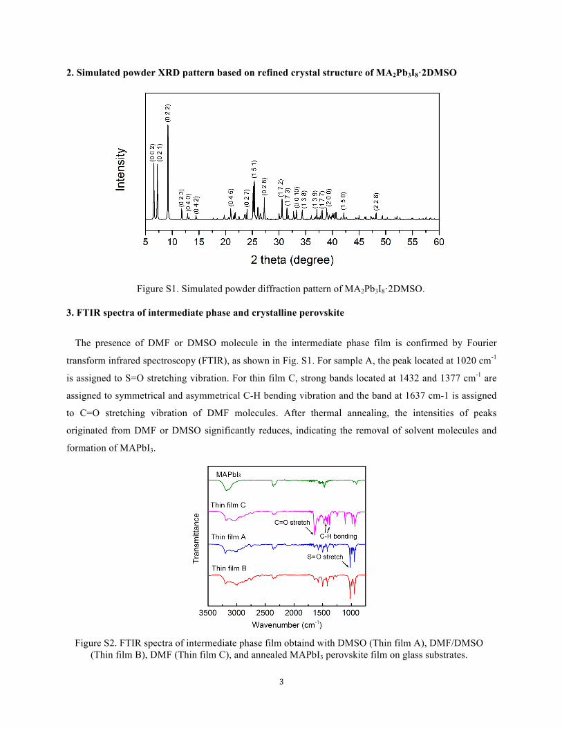
2. Simulated powder XRD pattern based on refined crystal structure of MA2Pb3I8·2DMSO
3. FTIR spectra of intermediate phase and crystalline perovskite
The presence of DMF or DMSO molecule in the intermediate phase film is confirmed by Fourier
transform infrared spectroscopy (FTIR), as shown in Fig. S1. For sample A, the peak located at 1020 cm-1
is assigned to S=O stretching vibration. For thin film C, strong bands located at 1432 and 1377 cm-1 are
assigned to symmetrical and asymmetrical C-H bending vibration and the band at 1637 cm-1 is assigned
to C=O stretching vibration of DMF molecules. After thermal annealing, the intensities of peaks
originated from DMF or DMSO significantly reduces, indicating the removal of solvent molecules and
formation of MAPbI3.
Figure S1. Simulated powder diffraction pattern of MA2Pb3I8·2DMSO.
!
! Figure S2. FTIR spectra of intermediate phase film obtaind with DMSO (Thin film A), DMF/DMSO (Thin film B), DMF (Thin film C), and annealed MAPbI3 perovskite film on glass substrates.
4
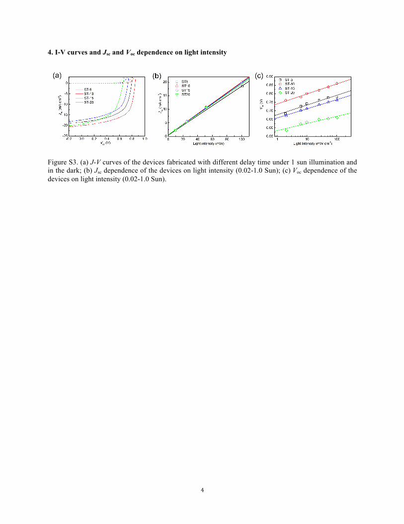
4. I-V curves and Jsc and Voc dependence on light intensity
Figure S3. (a) J-V curves of the devices fabricated with different delay time under 1 sun illumination and in the dark; (b) Jsc dependence of the devices on light intensity (0.02-1.0 Sun); (c) Voc dependence of the devices on light intensity (0.02-1.0 Sun).
5
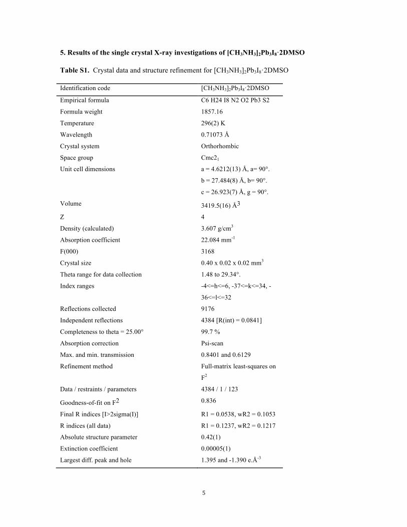
5. Results of the single crystal X-ray investigations of [CH3NH3]2Pb3I8·2DMSO
Table S1. Crystal data and structure refinement for [CH3NH3]2Pb3I8·2DMSO
Identification code [CH3NH3]2Pb3I8·2DMSO
Empirical formula C6 H24 I8 N2 O2 Pb3 S2
Formula weight 1857.16
Temperature 296(2) K
Wavelength 0.71073 Å
Crystal system Orthorhombic
Space group Cmc21
Unit cell dimensions a = 4.6212(13) Å, a= 90°.
b = 27.484(8) Å, b= 90°.
c = 26.923(7) Å, g = 90°.
Volume 3419.5(16) Å3
Z 4
Density (calculated) 3.607 g/cm3
Absorption coefficient 22.084 mm-1
F(000) 3168
Crystal size 0.40 x 0.02 x 0.02 mm3
Theta range for data collection 1.48 to 29.34°.
Index ranges -4<=h<=6, -37<=k<=34, -
36<=l<=32
Reflections collected 9176
Independent reflections 4384 [R(int) = 0.0841]
Completeness to theta = 25.00° 99.7 %
Absorption correction Psi-scan
Max. and min. transmission 0.8401 and 0.6129
Refinement method Full-matrix least-squares on
F2
Data / restraints / parameters 4384 / 1 / 123
Goodness-of-fit on F2 0.836
Final R indices [I>2sigma(I)] R1 = 0.0538, wR2 = 0.1053
R indices (all data) R1 = 0.1237, wR2 = 0.1217
Absolute structure parameter 0.42(1)
Extinction coefficient 0.00005(1)
Largest diff. peak and hole 1.395 and -1.390 e.Å-3
6
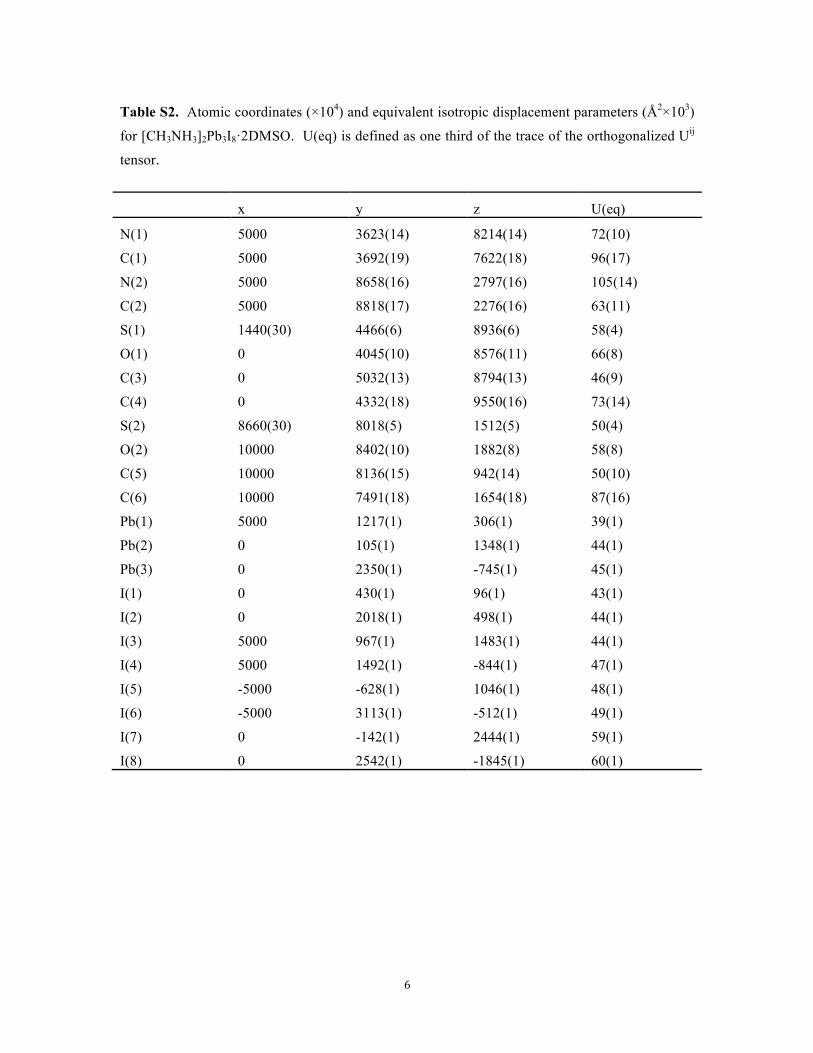
Table S2. Atomic coordinates (×104) and equivalent isotropic displacement parameters (Å2×10³)
for [CH3NH3]2Pb3I8·2DMSO. U(eq) is defined as one third of the trace of the orthogonalized Uij
tensor.
x y z U(eq)
N(1) 5000 3623(14) 8214(14) 72(10)
C(1) 5000 3692(19) 7622(18) 96(17)
N(2) 5000 8658(16) 2797(16) 105(14)
C(2) 5000 8818(17) 2276(16) 63(11)
S(1) 1440(30) 4466(6) 8936(6) 58(4)
O(1) 0 4045(10) 8576(11) 66(8)
C(3) 0 5032(13) 8794(13) 46(9)
C(4) 0 4332(18) 9550(16) 73(14)
S(2) 8660(30) 8018(5) 1512(5) 50(4)
O(2) 10000 8402(10) 1882(8) 58(8)
C(5) 10000 8136(15) 942(14) 50(10)
C(6) 10000 7491(18) 1654(18) 87(16)
Pb(1) 5000 1217(1) 306(1) 39(1)
Pb(2) 0 105(1) 1348(1) 44(1)
Pb(3) 0 2350(1) -745(1) 45(1)
I(1) 0 430(1) 96(1) 43(1)
I(2) 0 2018(1) 498(1) 44(1)
I(3) 5000 967(1) 1483(1) 44(1)
I(4) 5000 1492(1) -844(1) 47(1)
I(5) -5000 -628(1) 1046(1) 48(1)
I(6) -5000 3113(1) -512(1) 49(1)
I(7) 0 -142(1) 2444(1) 59(1)
I(8) 0 2542(1) -1845(1) 60(1)
7
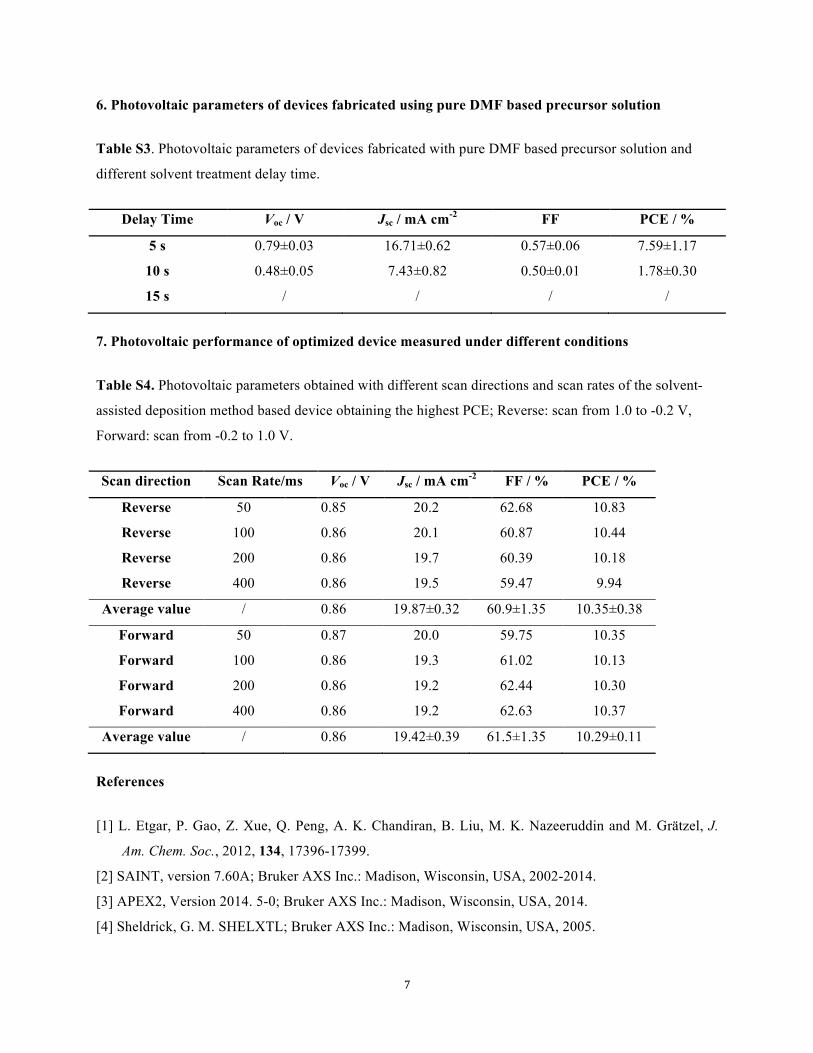
6. Photovoltaic parameters of devices fabricated using pure DMF based precursor solution
Table S3. Photovoltaic parameters of devices fabricated with pure DMF based precursor solution and
different solvent treatment delay time.
Delay Time Voc / V Jsc / mA cm-2 FF PCE / %
5 s 0.79±0.03 16.71±0.62 0.57±0.06 7.59±1.17
10 s 0.48±0.05 7.43±0.82 0.50±0.01 1.78±0.30
15 s / / / /
7. Photovoltaic performance of optimized device measured under different conditions
Table S4. Photovoltaic parameters obtained with different scan directions and scan rates of the solvent-
assisted deposition method based device obtaining the highest PCE; Reverse: scan from 1.0 to -0.2 V,
Forward: scan from -0.2 to 1.0 V.
Scan direction Scan Rate/ms Voc / V Jsc / mA cm-2 FF / % PCE / %
Reverse 50 0.85 20.2 62.68 10.83
Reverse 100 0.86 20.1 60.87 10.44
Reverse 200 0.86 19.7 60.39 10.18
Reverse 400 0.86 19.5 59.47 9.94
Average value / 0.86 19.87±0.32 60.9±1.35 10.35±0.38
Forward 50 0.87 20.0 59.75 10.35
Forward 100 0.86 19.3 61.02 10.13
Forward 200 0.86 19.2 62.44 10.30
Forward 400 0.86 19.2 62.63 10.37
Average value / 0.86 19.42±0.39 61.5±1.35 10.29±0.11
References
[1] L. Etgar, P. Gao, Z. Xue, Q. Peng, A. K. Chandiran, B. Liu, M. K. Nazeeruddin and M. Grätzel, J.
Am. Chem. Soc., 2012, 134, 17396-17399.
[2] SAINT, version 7.60A; Bruker AXS Inc.: Madison, Wisconsin, USA, 2002-2014.
[3] APEX2, Version 2014. 5-0; Bruker AXS Inc.: Madison, Wisconsin, USA, 2014.
[4] Sheldrick, G. M. SHELXTL; Bruker AXS Inc.: Madison, Wisconsin, USA, 2005.