Embed Size (px)
Citation preview
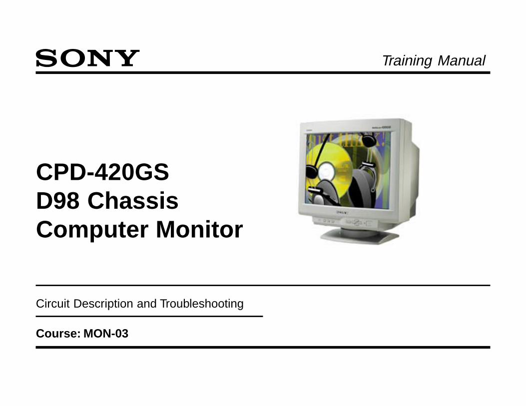
Training Manual
Circuit Description and Troubleshooting
Course: MON-03
CPD-420GSD98 ChassisComputer Monitor
S

D98 Chassis Specifications 1
Power Saving Function 2
Self Diagnosis Function 2
Timing Specification for CPD-420GS 3
Troubleshooting Safety 4
Overall Block 5
N Board 5
A Board 5
H Board 5
D Board 7
Power Supply 9
AC Input 9
AC Input Troubleshooting 9
EMI Filter 9
Degauss Circuit 9
Degauss Troubleshooting 9
Start Up and “Active On” Operation 11
Regulation 13
Secondary Voltages 15
“Active Off” and “Suspend/Standby” Operation 17
Secondary Voltages 19
Power Supply Protection Circuits 21
Table of ContentsOVP (Over Voltage Protection 21
UVP (Under Voltage Protection) 21
OCP (Over Current Protection) 21
Troubleshooting Protection Circuits 21
No Power Troubleshooting 23
Feedback Circuit Troubleshooting 23
The AN8037 Power supply Controller 25
Troubleshooting Short Circuit Protection 27
Troubleshooting Secondary Circuits 29
Rectifier Section Troubleshooting 29
Troubleshooting Horizontal Centering 29
+5V Standby Circuit 31
Troubleshooting +5V Standby Circuit 31
+12V Regulator 31
Troubleshooting +12V Regulator 31
Heater Voltage Regulator 33
Troubleshooting Heater Voltage 33
N Board 35
Micro Standby and Reset (N Board) 35
DSP Regulator 35
Video and OSD Processing 37
RGB Preamp 37

RGB Drive 39
RGB OUT 39
RGB CUTOFF 41
On Screen Display (OSD) 43
ASC (Auto Size and Center) 43
Sub Contrast (Cutoff) control 45
Brightness and Contract control 45
G2 control and Spot Killer 47
Color Restoration 49
Color Restoration Circuit (Red only) 49
Color Restoration Function (Red only) 49
GPE Graphic Picture Enhancement 51
Standard Mode 51
Presentation Mode 51
Graphic/Video Mode 51
Plug and Play 53
VGA 53
What is Plug and Play? 54
Display Data Channel Circuit 55
DDC1 55
DDC2B and DDC2AB 55
DDC Data Format (EDID) 57
Horizontal Deflection 59
Horizontal Drive 59
Horizontal AFC 61
Horizontal Size Control 63
Pin Keystone, Bow and Geometric Corrections 65
Horizontal Centering (Raster only) 67
Horizontal Linearity 69
Impedance Matching (S CAPS) 71
Horizontal Deflection Shutdown 73
Protection 73
High Voltage Circuit 75
High Voltage 75
High Voltage Regulation 75
G2 (Screen) Voltage 75
ABL (Auto Brightness Limiting) 77
HV Protection 79
HV Shutdown 79
ABL Shutdown 79
Dynamic Focus (DF) Circuit 81
Horizontal DF 81
Vertical DF 83
Vertical Deflection 85
Vertical Drive 85
Vertical Geometric Corrections 85
Vertical Centering 87
Vertical Feedback Pulse 87

Vertical Protection 89
Rotation and Vertical Key Circuits 91
Rotation 91
Vertical Key 91
Convergence Circuits 93
Static Convergence IC704 93
Dynamic Convergence IC701 95

1
D98 Chassis Specifications
Picture tube 0.25 - 0.27 mm aperture grill pitch19 inches measured diagonally90 - degree deflectionTrinitron
Video image area (18" maximum viewing image)Approx. 365 x 274 mm (w/h)(14 3/8 x 10 7/8 inches)
Resolution Horizontal: Max 1600 dotsVertical: Max 1200 lines
Standard image area Approx. 352 x 264 mm (w/h)(13 7/8 x 10 1/2 inches)
Input SignalVideo Analog RGB (75 ohms typical)
0.7 V p-p, PositiveSync External HD/VD, Composite
Polarity Free TTLVideo Composite (Sync on Green)0.3 V p-p, Negative
Power ConsumptionMaximum 130WNominal 100W
Deflection frequency Horizontal: 30 to 96 kHzVertical: 48 to 120 Hz
AC input voltage / current 100 to 120V, 50/60 Hz, 1.7 A220 to 240V, 50/60 Hz, 1.2 A
Dimensions 444 x 467 x 455 (w/h/d)(17 1/2 x 18 1/2 x 18 inches)
Mass Approx. 26 kg (57 lb 5 oz)
Plug and Play DDC/DDC2B(Front/Rear input)DDC2Bi (Rear input only)
Design and specifications are subject to change without notice.

2
POWER SAVING FUNCTIONThe monitor has three Power Saving modes. By sensing the absence ofa video signal from the computer, it reduces power consumption as fol-lows:
NOTE: If no video signal is input to the monitor, the “NO INPUT SIGNAL”message appears. After about 30 seconds, the Power Saving functionautomatically puts the monitor into active-off mode and the indicator lightsup orange. Once the monitor detects horizontal and vertical sync signals,the monitor automatically resumes normal operation mode.
SELF DIAGNOSIS FUNCTION
When a failure occurs, the STANDBY/TIMER lamp will flash a set of num-ber of times to indicate the possible cause of the problem. If there is morethan one error, the lamp will identify the first of the problem areas.
Status Area of Failure LED Indication1 Failure 1 HV or B+ Orange (0.5 second)/Off (0.5 second)2 Failure 2 H Stop, V Stop, Thermal Orange (1.5 second)/Off (0.5 second)3 Failure 3 ABL Orange (0.5 second)/Off (1.5 second)4 Aging/Self Test Orange (0.5 second)/Off (0.5 second)
Green (0.5 second)/Off (0.5 second)
S ta te P o w e rC o n s u m p t io n
R e q u ire d R e c o v e ryT im e
P o w e r In d ic a to r
1 N o rm a l O p e ra t io n ≤ 1 3 0 W — G re e n o n2 S ta n d b y (1 s t m o d e ) ≤ 1 5 W A p p ro x . 5 s e c . G re e n a n d o ra n g e a lte rn a te3 S u s p e n d (2 n d m o d e ) ≤ 1 5 W A p p ro x . 5 s e c . G re e n a n d o ra n g e a lte rn a te4 A c tiv e -o ff (3 rd m o d e ) ≤ 8 W A p p ro x . 5 s e c . O ra n g e5 P o w e r-o f f 0 W — O ff6 F a ilu re m o d e s — — S e e S e lf D ia g n o s is F u n c tio n
3
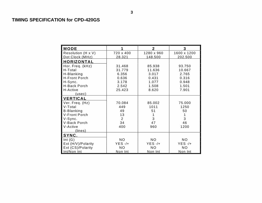
TIMING SPECIFICATION for CPD-420GS
MODE 1 2 3Resolution (H x V) 720 x 400 1280 x 960 1600 x 1200Dot Clock (MHz) 28.321 148.500 202.500HORIZONTALHor. Freq. (kHz) 31.468 85.938 93.750H-Total 31.779 11.636 10.667H-Blanking 6.356 3.017 2.765H-Front Porch 0.636 0.431 0.316H-Sync. 3.178 1.077 0.948H-Back Porch 2.542 1.508 1.501H-Active
(usec)25.423 8.620 7.901
VERTICALVer. Freq. (Hz) 70.084 85.002 75.000V-Total 449 1011 1250B-Blanking 49 51 50V-Front Porch 13 1 1V-Sync. 2 3 3V-Back Porch 34 47 46V-Active
(lines)400 960 1200
SYNC.Int (G) NO NO NOExt (H/V)/Polarity YES -/+ YES -/+ YES -/+Ext (CS)/Polarity NO NO NOInt/Non Int Non Int Non Int Non Int

4
Troubleshooting Safety
WARNING:Before attempting to repair the power supply or any other circuit, safetyshould be considered first . Never connect test probes to the primaryside circuits unless proper isolation has been provided. If isolation forthe AC main input is not provided, serious harm can result . Never as-sume you are safe.
Troubleshooting HINT:Visual inspection can play an essential part in any troubleshooting tech-nique. A Visual inspection of components can lead to the problem areaand the repair of the circuit at fault. Your eyes may be your best trouble-shooting tools to use.

5
Overall Block
N BoardThe N Board is mounted to the D Board via connectors CN1001 andCN801. The Microprocessor IC1001, EEPROM IC1005 and the DSP(Digital Signal Processor) IC1002 are located on the N board. IC1001receives control inputs from the front panel buttons (H board) and thefront and rear video inputs via the A board. IC1001 responds to the Tim-ing and Sync parameters of the video inputs. IC1001 communicates withIC1005 via the I2C bus. IC1005 contains the operation, set up, factorypreset and user preset data and is utilized by IC1001 to control the moni-tor circuits and to match the operating parameters to the input signals.IC1001 also controls IC1002 via the I2C bus and provides IC1002 with thenecessary timing and sync parameters.
IC1001 directly controls Input switching, Rotation, H. Cent, H Lin Bal,Degauss, Power Shutdown, Heaters, Remote On/Off and S Caps (Im-pedance Matching). IC1001 controls the Power Save Function, OSD (OnScreen Display) and RGB DRIVE (A board). IC1001 also provides com-munication with DAS (Digital Alignment Software), CATS (Color Adjust-ment Tool for Service) and the DDC (Display Data Channel).
IC1002 outputs Deflection Drive, Convergence and Geometry CorrectionWaveforms to their respective circuits located on the D board.
A BoardThe main function of the A Board is to receive incoming video signals andprocess them into RGB video drives for the CRT. Video signals can bereceived either from the conventional 15 D-sub connector or via an addi-tional 15 D-sub female connector input located on the front of the monitor.The purpose of this second input is to allow easy hookup to a laptopcomputer (video cable provided).
The A Board circuitry buffers the Sync timing signals and provides OSDvideo. The Timing Analysis for the ASC (Auto Size Center) function andthe Analog to Digital conversion for the Color Restoration function arealso processed. Additional functions include the DDC information to theDDC equipped host computer and all CRT cathode operating voltagessuch as Heater, G2 (Screen) and Focus are either processed or passedto the CRT.
H BoardThe User controls are located on the front bezel assembly of the monitorand provide the user with control of various monitor operations and func-tions. The LED provides the user with feedback as to the Power Savingand Failure condition of the monitor.

6

7
D Board(Power Supply)The Power Supply, which is located on the D Board, operates very similarto previous monitor chassis design such as the D1 chassis. This unitincorporates the use of a switch mode power supply. It has both PWMand RCC characteristics. The Power Supply has four modes of opera-tion. Except for the AC power switch, three modes are controlled byIC1001 (N Board). The modes of operation are ‘Off’, ‘Active Off’, ‘Sus-pend/Standby’ and ‘Active On’. These modes are related to the PowerSaving and Self Diagnosis functions. The Power supply provides all thenecessary operating voltages along with Horizontal Centering and CRTHeater voltages.
(Deflection)The Horizontal and Vertical deflection circuits along with Horizontal Cen-tering, Size, Rotation and Tilt are located on the D Board. The N Boardprovides these circuits with the necessary size, position and geometryparameters as required by the different video timing conditions and useradjustments. Impedance matching (S Caps) and Horizontal Linearity arealso performed in the Horizontal deflection circuit as required by the dif-ferent video timing conditions.
(Convergence)Both Static and Dynamic Convergence circuits are located on the D Board.The N Board provides these circuits with the necessary geometry param-eters as required by the different video timing conditions and user adjust-ments. The convergence circuits provide two-dimensional (H and V) cor-rection patterns that are applied to the convergence yoke.
(High Voltage)The HV generation and regulation circuits are located on the D Board.The N Board provides the HV circuits with the necessary drive param-eters required by the different video timing conditions. The HV circuitprovides the CRT with Anode, Focus and Screen voltages required forproper CRT operation.
The D98 chassis is also equipped with Dynamic Focus circuitry locatedon the D Board. The Dynamic Focus circuit, controlled by the N Board,provides the necessary focus control voltage for the outer edge areas ofthe screen as required by the different video timing conditions.

8

9
OverviewThe power supply in this unit is a switch mode power supply. The powersupply is rated to operate with an AC input voltage range of 100V - 240V.Current input is 1.2 - 1.7 A. The output of the power supply produces+180V, +80V, ±16V, +12V and +5V DC from the AC input. In addition, itprovides +6.3V DC for the CRT Heater and an isolated ±8V DC output tothe Horizontal Centering circuits. It has a fold back mode used for thePower Saving and Failure (Shutdown) operations. This chassis incorpo-rates the use of a single power supply control IC601. IC601 providesmost of the power supply control except for output power switching pro-vided by Q602 (POWER SWITCH).
AC InputThe AC input section provides EMI filtering, input protection, surge limit-ing and CRT degauss operation.
AC Input TroubleshootingFor No Power or Dead Set condition, the AC Input circuitry should bechecked. F601 should be checked for continuity. CN603 to the H Boardand the AC power switch S601 should be checked for continuity. Furtherchecks should be made to R602, TH600 and D601 respectively if no prob-lems can be identified.
EMI FilterThe EMI filter comprises X - capacitors C601 and C602, Y - capacitorsC603, C604, C605 and C606 and the line filter transformer LF602. Inputprotection is provided by F601 and surge current limiting by thermistorTH600 and resistors R602 and R603.
Degauss CircuitThe Degauss Circuit is used to demagnetize or degauss the CRT. During‘Active On’ mode, the Micro IC1001/5 (N Board) sets the Degauss signalto digital H (+5V). The Degauss signal via CN1001 pin 25 to CN801 pin25 (D Board) is applied to Q670 (DEGAUSS SW). Q670 turns ON andactivates relay RY601. This allows AC current to flow to the degauss coilthrough posistor THP602. The current heats up THP602 posistor and itsaffective resistance increases. This dampens the current in the degausscoil to nearly zero allowing the magnetic field to decay gradually. Afterapproximately 5 seconds, IC1001/5 sets the Degauss signal to digital L(0V). The Degauss signal via CN1001/25 to CN801/25 (D Board) is ap-plied to Q670 (DEGAUSS SW). Q670 turns OFF and deactivates relayRY601. The degauss coil should sufficiently demagnetize the CRT.
Degauss TroubleshootingThe malfunction of the degauss circuit can be a loss of the degauss signalfrom the N Board. The +5V DC degauss signal can be checked at CN801/25 and should be present for approximately five seconds once AC poweris applied. The activation of RY601 through Q670 can also be heard.Further checks to THP602 and VA601 should be checked respectively.
Another method of verifying the degauss circuit operation is to use themanual degauss operation found in the OSD menu.
Power Supply

10
CN2003
E1
4
H BOARD
S602
CN603
2 1
3 4
FB608
FB609R603
1
F1
1
25
25
N BOARDIC1001/5
CN1001
12V
D670
R672
Q670 R670
R671
CN 801
G
N
L
C605
C606
C601
LF602
R601
C602
C604
C603
FB607D601
R602 TH600
4
1
4
11
11
THP602
VA601
CN601
D BOARD
RY601
F601 4A250V
AC
IN
CN610G N D
!
D98MON
DEGAUSS
T OT601
+Q602
AC INPUT
+
+
+ + ++
P O W E RS W I T C H
DE
GA
US
S C
OIL

11
Start Up and ‘Active On’ OperationThe Power Supply uses a flywheel type switch mode supply. It has bothPWM and RCC (Resistor and Capacitor) characteristics. The PWM con-trols the pulse width of the gate drive. The RCC portion insures that thenext conduction cycle starts at zero volts. Therefore, the gate pulse widthvaries and the switching frequency varies.
When Power switch S601 (H Board) is closed, AC (100V - 240V) is ap-plied to D601 full wave rectifier. +160V DC (110V AC in) is applied throughR603, L604 and R615 to T601/5 (SWITCHING TRANSFORMER). Startup current is supplied from D601 (half wave rectified), through R613 toIC601/7 (VCC). Start up voltage at IC601/7 is approximately +12V DC.
Once start up voltage is applied, IC601/6 (OUT) outputs PWM drive to thegate of Q602 (POWER SWITCH). The PWM frequency will vary between65kHz to 120kHz depending upon input voltage and power level. ThePWM drive from Q602 is applied to T601/2. T601 develops all the sec-ondary operating voltages. After start up, the output from T601/8 throughR623 is rectified by D605 and provides VCC +17V DC through D624 andD657 to IC601/7 during normal ‘Active On’ operation.
IC601/6 PWM
Q602/Drain

12

13
RegulationOverall regulation is accomplished by varying the feedback voltage toIC601/9 (FB). The secondary +16V DC supply via R631, D614 and R658provide IC603/1 with a reference voltage. The secondary +180V DC sup-ply is voltage divided by R659, R663 and R660 to provide IC652/1 (ER-ROR AMP) with a sample of the +180V DC supply.
IC1001/7 (N Board) ‘REMOTE ON/OFF’ command is set H (+5V) whichturns Q656 ON and turns Q658 OFF, this allows IC652/3 to control feed-back. IC652 is a shunt regulator and controls the current through IC603pin 1 and pin 2. Any change in the B+ voltage will cause IC652 pin 3 tovary in voltage inversely proportional to the B+.
IC652/3 is applied to IC603/2 to control the feedback output of IC603/4while maintaining electrical isolation between chassis ground and AC in-put ground. The signal at IC603/4 is applied to IC601/9 (FB). As a result,IC601/6 responds accordingly to adjust the duty cycle and frequency out-put applied to Q602 by regulating the secondary B+ (+180V DC) voltage.
IC601/6 PWM
Q602/Drain

14

15
Secondary VoltagesThe following voltages are produced by T601 SRT.
1. The output at T601/13 is rectified by D650 to produce +183V DC usedfor deflection and video circuits.
2. The output at T601/14 is rectified by D651 to produce +80V DC usedfor video circuits.
3. The output at T601/16 is rectified by D652 and D655 to produce +16VDC and +16V-2 DC used for deflection, +5/+12V Regulator IC605.
4. The output at T601/17 is rectified by D654 to produce +7V DC usedfor +5/+12V Regulator IC605 and +6.3V Heater regulator IC604.
5. The output at T601/18 is rectified by D653 and D656 to produce -16VDC and -16V-2 DC used for the deflection circuits.
6. The output at T601/10 through R621 is rectified by D648 to producethe H+ used for Horizontal Centering.
· The output at T601/12 through R622 is rectified by D649 to producethe H- used for Horizontal Centering.
· The output at T601/11 is used for the H+ and H- floating ground refer-ence. The H+ and H- voltages in reference to floating ground are±8V.
NOTE: Care should be taken not to short the floating ground to the sec-ondary ground.
SECONDARY VOLTAGESOUTPUT OFF 'Active OFF' 'Suspend/Standby' 'Active ON'
B+ 0 +145V +145V +183V+80V 0 +62V +62V +80V+16V 0 +9V +9V +16V-16V 0 -12V -12V -16V+12V 0 0 0 +12V+8V 0 +5.5V +5.5V +7V+5V 0 +5V +5V +5V
Heaters 0 0 +3.2V +6.3VH. Centering 0 ±5V ±5V ±8V

16

17
‘Active Off’ and ‘Suspend/Standby’ OperationThe power supply enters the ‘Active Off’ and ‘Suspend/Standby’ modeunder the following conditions…
1. Loss of H and/or V Input Sync signals
· LED illuminates Orange
2. Loss of Horizontal Deflection feedback
· LED illuminates Orange (1.5 seconds) / Off (0.5 seconds)
3. Loss of Vertical Deflection feedback
· LED illuminates Orange (1.5 seconds) / Off (0.5 seconds)
4. If Beam current (ABL) becomes excessive
· LED illuminates Orange (0.5 seconds) / Off (1.5 seconds)
5. If HV becomes excessive
· LED illuminates Orange (0.5 seconds) / Off (0.5 seconds)
6. Loss of secondary voltages
· LED illuminates Orange (0.5 seconds) / Off (0.5 seconds)
The ‘Active Off’ and ‘Suspend/Standby’ modes are controlled by the ‘RE-MOTE ON/OFF’ signal from the Micro IC1001/7 (N Board). Feedback isprovided by circuit elements IC603, D631, D632, R662, Q656 and Q658.During ‘Active Off’ and ‘Suspend/Standby’ modes, the ‘REMOTE ON/OFF’signal from IC1001/7 is L (0V) and is applied to Q656 turning it OFF, thusturning Q658 on to disable IC652. Current flows through Q658 (E - B),R662 and D632 biasing Q658. This allows standby current to flow throughIC603 pin 1 and pin 2, D631 and Q658 (C - E). The output of IC603/4outputs sink current from IC601/9 (FB). As a result, IC601/6 respondsaccordingly to adjust the duty cycle and frequency output applied to Q602in order to produce the reduced unregulated output voltages.
IC601/6 PWM
Q602/Drain

18

19
Secondary VoltagesUnder ‘Active Off’ and ‘Suspend/Standby’ modes, the following voltagesare produced by T601.
1. The output at T601/13 is rectified by D650 to produce +145V DC usedfor deflection and video circuits.
2. The output at T601/14 is rectified by D651 to produce +62V DC usedfor video circuits.
3. The output at T601/16 is rectified by D652 and D655 to produce +9VDC and +9V-2 DC used for deflection, +5/+12V Regulator IC605.
4. The output at T601/17 is rectified by D654 to produce +5.5V DC usedfor +5/+12V Regulator IC605 and +6.3V Heater regulator IC604.
5. The output at T601/18 is rectified by D653 and D656 to produce -12VDC and -12V-2 DC used for the deflection circuits.
6. The output at T601/10 through R621 is rectified by D648 to producethe H+ used for Horizontal Centering.
· The output at T601/12 through R622 is rectified by D649 to producethe H- used for Horizontal Centering.
· The output at T601/11 is used for the H+ and H- floating ground refer-ence. The H+ and H- voltages in reference to floating ground are±5V.
NOTE: Care should be taken not to short the floating ground to the sec-ondary ground.
SECONDARY VOLTAGESOUTPUT OFF 'Active OFF' 'Suspend/Standby' 'Active ON'
B+ 0 +145V +145V +183V+80V 0 +62V +62V +80V+16V 0 +9V +9V +16V-16V 0 -12V -12V -16V+12V 0 0 0 +12V+8V 0 +5.5V +5.5V +7V+5V 0 +5V +5V +5V
Heaters 0 0 +3.2V +6.3VH. Centering 0 ±5V ±5V ±8V

20

21
Power Supply Protection Circuits
OVP (Over Voltage Protection)During normal ‘Active On’ operation, the output of T601/8 through R623 isrectified by D605 and provides +17V DC through D624 and D657 to IC601/7 (VCC). In the event that the regulation or feedback loops fail, the sec-ondary output voltages may rise rapidly. The output of T601/8 would alsorise and is sensed at IC601/7 (VCC) which internally has a threshold ofapproximately +19V DC. Once this threshold is reached, IC601/6 willlatch to eliminate drive to Q602, resulting in power supply shut down.Once IC601 is latched, you must turn the AC power OFF and ON again torestart the power supply.
UVP (Under Voltage Protection)The input at IC601/7 (VCC) is also used to sense an Under Voltage con-dition. Under Voltage occurs when the input at pin 7 (VCC) is less than+9.5V DC. Once this threshold is reached, IC601 will latch and disablethe output at pin 6 (OUT) going to Q602 resulting in power supply shutdown. Once IC601 is latched, you must turn the AC power OFF and ONagain to restart the power supply.
OCP (Over Current Protection)OCP is activated if there is excessive current passing through Q602(POWER SWITCH). R609 is used for current sensing. Current throughR609 will cause a negative voltage drop in reference to HOT ground.R608, R606 and C615 couples this voltage drop to IC601/4 (CLM). Shouldthis voltage level exceeds -0.18V, IC601 will enter the cycle by cycle cur-rent limiting mode.
To prevent premature OCP sensing, Q605 and IC606 provide a Soft Startto IC601/2 (CCP) to prevent OCP during start up.
Troubleshooting Protection CircuitsEach protection circuit can be isolated to their respective defect. Thepower supply can be operated in the “Active Off’ mode to better trouble-shoot each circuit under reduced voltage condition by simply removingthe N Board.

22

23
No Power Troubleshooting(IC601 Troubleshooting)First apply AC to the monitor and check IC601/6 output. If the output atpin 6 is not present or briefly appears there could be problems with Q602and related components. Check VCC at IC601/7. If the voltage is lessthan +9V DC, IC601 could be in the latch mode. If the voltage is very low,R613, R623, D605, D624 and D657 should also be checked respectively.If no problems can be identified, in reference to Hot ground, check theimpedance of each pin at IC601. If any of these pins are shorted, replaceIC601 and check components connected to the related pins. Take carethat C616 and C619 are fully discharged before replacing IC601.
(Q602 Troubleshooting)Q602 can be damaged in various ways such as voltage, current and tem-perature. Check Q602 for shorts. Further checks to F601, R609 andR615. Additional components to check are D603, D604 and IC601. Thereis also a clamp circuit, which is used to clip the turn off spike found onQ602 (D). Check D615, C624 and R619.
Feedback Circuit TroubleshootingProblems with the feedback circuits can cause power supply shut downor low voltages. First determine whether the power supply is operating in‘Active Off’, ‘Active On’ modes or not at all.
The power supply can be stuck in ‘Active Off’ mode. The Remote ON/OFF signal from the N Board, Q656, Q658, IC603 and IC652 can affectthis condition. In addition, check the protection circuits.
IC601/6 PWM
Q602/Drain

24

25
The AN8037 Power Supply Controller
IC601The heart or the primary section is the AN8037 Power Supply Controller,IC601. The following table describes the function of each pin.
Pin 1 -TR
This is TR or Transformer Reset. Similar to a demagnetization function, this pin detects the falling edgeof the primary waveform during relaxation period. It allows the next conduction pulse only afterreaching the bottom of the ringing waveform.
Pin 2 -OCP
Over current protection. Used to determine the overload level at which the timer latch is activated.
Pin 3 -CF
Oscillator. W ith a capacitor, determines the switching frequencies. (On/Off times)
Pin 4 -CLM
Over current protection. If the voltage on this pin (primary current feedback) exceeds -0.18V, the powersupply will enter cycle by cycle current limiting mode.
Pin 5 -GND
IC ground terminal.
Pin 6 -OUT
Output driver for switching transistor Q602.
Pin 7 -VCC
IC601 supply voltage terminal. This voltage is normally +17.5V DC during 'Active On' mode and +12VDC during 'Active Off' and 'Suspend/Standby' mode. The IC receives starting current via startupresistor R613 until the auxiliary supply is available from T601 VCC winding. If the voltage on this pinexceeds +19.4V DC, OVP is activated and the power supply shuts off and can only be restarted bydisconnecting and reconnecting the AC line. Under voltage lock out (UVP) occurs when the voltage isless than +9.5V DC.
Pin 8 -SD
Used for the OVP and timer latch functions. A capacitor determines the timing for OVP function.
Pin 9 -FB
Feedback terminal.

26

27
Secondary Short Circuit ProtectionShort Circuit Protection for the secondary low voltage supplies are de-tected in different ways.
1. The “B+ DET” line is used to detect the loss of the -16V DC supplythrough circuit elements R611 and R612. R611 is connected to the+5V DC from IC605 and R612 is connected to the -16V DC supplyfrom T601. The node voltage between R611 and R612 is monitoredby the Micro IC1001/14 (N Board). If the node voltage exceeds +2VDC, IC1001/6 goes H (+5V) turning Q657 ON, shunting normal regu-lation feedback. This causes IC601 to increase the drive output to thepoint of OVP latch via pin 7(VCC).
Note: LED illuminates Orange (0.5 seconds) / Off (0.5 seconds)
2. The +16V, +12V and +5V DC secondary voltages are monitoredthrough circuit elements D641, Q640 and R641. The +80V DC fromT601 through R641 is applied to Q640 (C). Normally the +5V DCfrom IC605 and D641 turns Q640 ON and Q657 OFF. If there is asubstantial short circuit on any of the secondary low voltage supplies,the +5V DC standby supply can be attenuated. If it goes lower than+3V DC, Q640 will turn OFF. With Q640 OFF, Q657 turns ON tobypass the feedback voltage from IC603. This causes IC601 to in-crease the drive output to the point of OVP latch via pin 7.
Troubleshooting Short Circuit ProtectionThe power supply can be operated in the “Active Off’ mode to better trouble-shoot each circuit under reduced voltages by simply disabling the ‘RE-MOTE ON/OFF’ line from the N Board by lifting pin 16 of CN801. Q640and Q657 should be check respectively.

28

29
Troubleshooting Secondary CircuitsFailures in these sections are interrelated and one circuit can affectanother. Consequently, some failures will also affect the primary cir-cuit.
Rectifier Section TroubleshootingRectifier diode failures are not common, but do occur. Deflection (DBoard), Video (A Board) and N Board failures contribute to diode dam-age. In the event, a voltage is not present, check for shorts to ground oropen or shorted diodes. Also, check for any open fusible resistor andshorted zener diodes found on the supply lines.
Troubleshooting Horizontal CenteringA loss of the Horizontal Centering adjustment can be caused by the fail-ures of rectifier diodes, fusible resistors, IC502 and related components.Measure the +/- voltages in reference to the horizontal centering ground(HN). Typically, the voltages are ±8V DC. However, the adjustment set-ting can reduce the voltages by approximately 1V. If there are no prob-lems found at the Horizontal Centering supply, troubleshoot the Horizon-tal Centering circuitry.

30

31
+5V Standby CircuitDuring ‘Active Off’ and ‘Suspend/Standby’ modes, the +8V DC secondarysupply applied to IC605/1 (INPUT1) and Q601/C is reduced to +5.5V DC.In order to prevent loss of the +5V DC Standby, it is necessary to supplya back up voltage.
During ‘Active Off’ mode, the +16V DC secondary supply source is re-duced to +9V DC and is applied Q601/E. Q607 is OFF which turns Q606and Q601 ON. Q601 then outputs +9V DC to provide power to IC605/1(INPUT1). Finally, at the same time, IC605/7 (OUTPUT1) outputs regu-lated +5V DC.
During normal operation, the +8V DC supply is used to provide VCC volt-age to IC605/1. The “Back-up” supply circuit (Q601) is shut down via the‘REMOTE ON/OFF’ command from IC1001/7.
Troubleshooting +5V Standby CircuitThe loss of the +5V DC Standby voltage may appear as a no powersymptom. Check the +16V DC source, R617, Q601, Q606, Q607,IC605 and related components. Check the +8V DC source, D654,R654 and D610.
+12V RegulatorDuring ‘Active Off’ and ‘Suspend/Standby” modes, the +16V DC supply isreduced to +9V DC and is applied to IC605/2 (INPUT2). The ‘REMOTEON/OFF’ control signal from IC1001/7 is L and is routed to IC605/3 (DIS-ABLE), which disables the +12V DC regulated output.
During ‘Active On’ modes, the +16V DC supply is applied to IC605/2 (IN-PUT2). The ‘REMOTE ON/OFF’ control signal from IC1001/7 is H (+5V)and is routed to IC605/3 (DISABLE) to enable the +12V DC output at pin6 (OUTPUT2).
Troubleshooting +12V RegulatorDuring the ‘Active On’ mode, confirm the presence of +12V DC at IC605/6 (OUTPUT2). If missing, verify that a H is present at IC605/3 (DIS-ABLE).

32

33
Heater Voltage RegulatorHeater filament voltage is developed by the +8V DC supply to IC604/1 (I).During ‘Active On’ mode, IC1001/8 (N Board) outputs the “HEATER” con-trol line H (+5V) which is routed to IC604/4 (VC) to enable the +6.3V DCHeater supply voltage output at pin 2.
During ‘Standby/Suspend’ mode, the power supply is operated at reducedvoltages. As a result, the input voltage to IC604/4 (VC) is +5.5V DC. Theoutput from IC604/2 is also reduced to +3.2V DC keeping the heaters ofthe CRT active on during the power saving function. This allows the CRTto quickly display the information or video during the ‘Standby/Suspend’to ‘Active On’ transition.
During ‘Active Off’ mode, IC1001/8 (N Board) outputs a L (0V) to IC604/4(VC) disabling the +6.3V DC Heater supply voltage.
Troubleshooting Heater VoltageA loss of Heater Voltage will result in a no picture condition. During ‘ActiveOn’ mode, confirm IC1001/8 (N Board) outputs ‘HEATER’ control line H(+5V) to IC604/4 (VC) to enable the +6.3V DC Heater supply voltage.Also check for shorts or an open on the A Board and the CRT.

34

35
N Board
Micro Standby and Reset (N Board)The +5V DC Standby supply from IC605 (D Board) is routed to IC1001pin 11 and pin 31 providing VCC operating voltage. The +5V DC standbysupply is also applied to the RESET IC1003/1. IC1003 produces a “Re-set” pulse at pin 3 when the unit is first turned ON. The 8Mhz masterclock is developed by X1001 IC1001 pin 44 and pin 45.
When the unit is first powered ON, the Degauss command line of IC1001/5 goes H (+5V) for approximately 5 seconds then returns to a logic L (0V).At the same time, the ‘REMOTE ON/OFF’ command from IC1001/7 goesH (+5V). This signal is routed to the D Board via CN801/16 to enable the‘Active On’ mode of the power supply.
DSP RegulatorThe DSP IC1002 requires +3.3V DC for proper operating. IC1006/3 (O)outputs regulated +3.3V DC to IC1002 pins 9,12, 28 and 52. IC1003provides IC1002/54 (RESET) with a delayed “RESET” H (+5V) via R1105.The DSP outputs Deflection Drive, Convergence and Geometry Correc-tion Waveforms to their respective circuits located on the D board.
NOTE: With AC power applied, the output waveforms from the Micro andDSP should always be present.

36

37
Video and OSD Processing
RGB PREAMPThe RGB PREAMP IC008 receives the RGB and Sync signals from twosources. One is the conventional 15 D-sub connector and the other is the15 D-sub female connector input located on the front of the monitor. Thepurpose of this second input is to allow easy hookup to a laptop com-puter. The RGB signals from the conventional 15 D-Sub connector areinput to IC008 pin 2 (B), pin 5 (G) and pin 7 (R). The Sync signals areinput to IC008 pin 8 (H) and pin 9 (V).
The RGB signals from the additional 15 D-Sub female connector are in-put to IC008 pin 11 (B), pin 13 (G) and pin 16 (R). The Horizontal andVertical Sync signals are input to IC008 pin 17 (H) and pin 18 (V).
IC008 switches between inputs selected by the user via the front panelbutton. IC1001/1 (N Board) logic output selects the input source viaCN1004/2 to CN309/2 ‘INPUT SW’ to the A Board. The ‘INPUT SW’ sig-nal is routed to IC008/19 (SW) to select the conventional 15 D-Sub con-nector input or to select the 15 D-Sub female connector from the frontpanel.
The V OUT Sync signal from IC008/21 (V OUT) is routed to the N Board.The H OUT Sync signal from IC008/22 (H OUT) is input to the H DRIVEBUFFER IC006 pin 8 and pin 9. IC006 buffers the H OUT signal which isoutput at pin 4 is routed to the N Board.
CN309/5 VS OUT
CN309/7 H SYNC
The R G B input signals are then buffered and output from IC008 pin 27(R OUT), pin 30 (G OUT) and pin 35 (B OUT) to IC001.
IC008/27 R OUT

38

39
RGB DRIVEThe RGB outputs from IC008 are input to the RGB DRIVE IC001 pin 7 (BIN), pin 9 (G IN) and pin 11 (R IN). The G signal is also low pass filteredand input to IC001/10 (SYNC IN). The Sync on Green signal is pro-cessed and output at IC001/30 (C.SYNC) as composite sync which isrouted to the N Board. IC1001 (N Board) also provides IC001 pin 12(CLAMP) and pin 18 (BLK) with the necessary Clamping and Blankingsignals required from the Timing and Sync parameters of the video input.IC001 outputs the R G B signals at pin 20 (R OUT), pin 24 (G OUT) andpin 27 (B OUT).
CN309/1 C BLK
CN309/3 CLP
RGB OUTThe RGB outputs from IC001 are applied to RGB OUT IC002 pin 8 (R.IN), pin 9 (G. IN) and pin 11 (B. IN). IC002 provides the final amplifierstage for the RGB video signals. The output of IC002 pin 1 (B. OUT), pin3 (G. OUT) and pin 5 (R. OUT) drive the CRT cathodes via AC coupling.The output drive levels are approximately 45V p-p.
IC001/20 R OUT
IC002/5 R OUT

40

41
RGB CUTOFFThe RGB Cutoff levels can only be adjusted via the DAS/CATS softwareor by the Color Restoration function (explained later). IC1001 on the Nboard, via the I2C data bus controls IC001 D/A outputs at pin 3 (R BKG),pin 4 (G BKG) and pin 5 (B BKG). The D/A outputs from IC001 are inputto CUTOFF AMP IC004 pin 1 (B.IN), pin 3 (G.IN) and pin 4 (R.IN) whichsets the CRT Red, Green and Blue cathode DC cutoff level. The outputof IC004 pin 7 (R.CUT), pin 10 (G.CUT) and pin 13 (B.CUT) clamp theCRT Red, Green and Blue cathodes. The +180V DC with pull-up resis-tors R109, R209 and R309 and D106, D206 and D306 form the voltagedivider network for the R G B cutoffs respectively.

42
43
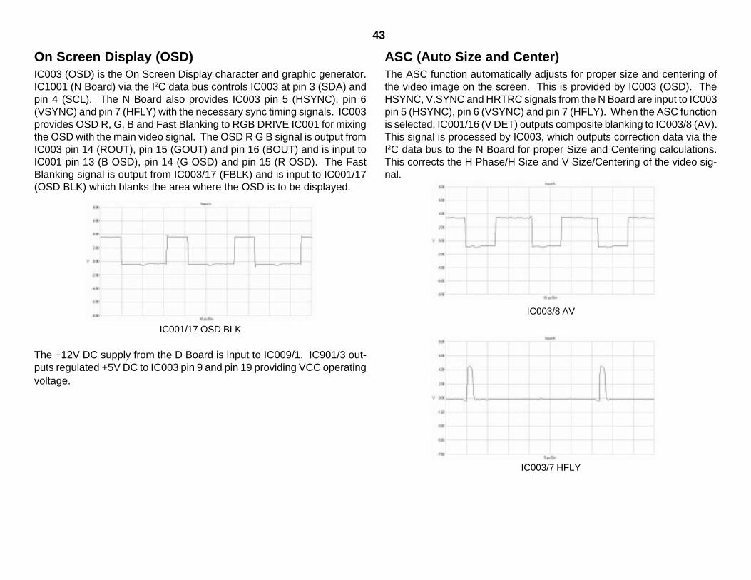
On Screen Display (OSD)IC003 (OSD) is the On Screen Display character and graphic generator.IC1001 (N Board) via the I2C data bus controls IC003 at pin 3 (SDA) andpin 4 (SCL). The N Board also provides IC003 pin 5 (HSYNC), pin 6(VSYNC) and pin 7 (HFLY) with the necessary sync timing signals. IC003provides OSD R, G, B and Fast Blanking to RGB DRIVE IC001 for mixingthe OSD with the main video signal. The OSD R G B signal is output fromIC003 pin 14 (ROUT), pin 15 (GOUT) and pin 16 (BOUT) and is input toIC001 pin 13 (B OSD), pin 14 (G OSD) and pin 15 (R OSD). The FastBlanking signal is output from IC003/17 (FBLK) and is input to IC001/17(OSD BLK) which blanks the area where the OSD is to be displayed.
IC001/17 OSD BLK
The +12V DC supply from the D Board is input to IC009/1. IC901/3 out-puts regulated +5V DC to IC003 pin 9 and pin 19 providing VCC operatingvoltage.
ASC (Auto Size and Center)The ASC function automatically adjusts for proper size and centering ofthe video image on the screen. This is provided by IC003 (OSD). TheHSYNC, V.SYNC and HRTRC signals from the N Board are input to IC003pin 5 (HSYNC), pin 6 (VSYNC) and pin 7 (HFLY). When the ASC functionis selected, IC001/16 (V DET) outputs composite blanking to IC003/8 (AV).This signal is processed by IC003, which outputs correction data via theI2C data bus to the N Board for proper Size and Centering calculations.This corrects the H Phase/H Size and V Size/Centering of the video sig-nal.
IC003/8 AV
IC003/7 HFLY

44

45
Sub Contrast (Cutoff) controlThe Sub Contrast levels can only be set by the DAS/CATS software forWhite Balance adjustment. When Sub Contrast is adjusted, the MicroIC1001 (N Board) via the I2C bus instructs IC001 to vary the DC level ofpin 3 (R BKG), pin 4 (G BKG) and pin 5 (B BKG). The DC levels are theninput to CUTOFF AMP IC004 pin 1 (B.IN), pin 3 (G.IN) and pin 4 (R.IN).The output of IC004 pin 7 (R.OUT), pin 10 (G.OUT) and pin 13 (B.OUT)are used to set the DC level of the R G B cathodes respectively. The+180V DC with pull-up resistors R109, R209 and R309 and D106, D206and D306 form the voltage divider network for the R G B cutoffs respec-tively.
Brightness and Contract controlThe Brightness and Contrast levels can be controlled either by the user orvia DAS/CATS software. When Brightness is adjusted, the Micro IC1001(N Board) via the I2C bus instructs IC001 to vary the DC pedestal level ofthe RGB outputs. When Contrast is adjusted, IC001 varies the P-P am-plitude of the RGB outputs. IC001 outputs the RGB signal at pin 20 (ROUT), pin 24 (G OUT) and pin 27 (B OUT).
IC001/20 R OUT

46

47
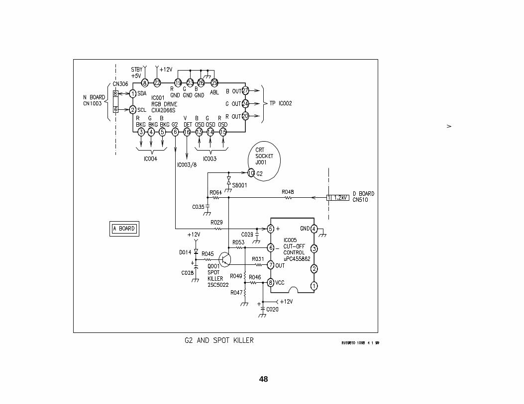
G2 control and Spot KillerThe G2 source voltage from the D board enters the A board via CN301/1via R048 and R064. The node between R048 and R064 is connected tothe CUTOFF CTRL circuit comprised of IC005 and Q001. The G2 adjust-ment can only be performed using the DAS/CATS Software or the ColorRestoration function (explained later). The Micro IC1001 (N Board) viathe I2C bus instructs IC001 to vary the DC level of pin 6 (G2). This volt-age is routed to the non-inverting input of IC005/5 (CUTOFF CTRL). TheDC output from pin 7 (OUT) is input to Q001/E and output at Q001/Cconfigured as a common base amplifier. Q001/C is connected to thenode between R048 and R064. By varying the DC voltage at this node,the DC level at J001/10 G2 of the CRT can be adjusted. C028 providesbias to Spot Killer Q001/B during power OFF, reducing the G2 voltage tominimum.
48

49
Color Restoration
OVERVIEWThe Color Restoration function can be performed by the user to restorethe White Balance of the CRT. The CRT beam current is measured whenWhite Balance is performed via the DAS/CATS software. The CRT beamcurrent is converted to a voltage and stored in registers. During the ColorRestoration function, these registers are sampled and the CRT beamcurrent is adjusted until they equal the values stored in the registers. TheColor restoration function can only be accessed via the OSD menu andactivated after an initial warm up period of approximately 30 minutes.
Color Restoration Circuit (Red only)The Color Restoration circuit is comprised of the Micro IC1001 (N Board),IC001 (RGB DRIVE), IC003 (OSD), IC004 (CUTOFF AMP), CRT and thecurrent sensing components. Each of the Red, Green and Blue cathodebeam current sensing circuits are identical and only the Red cathode beamcurrent circuit will be explained.
As the video image changes, the Red cathode beam current also changes.This current change flows through R116, R122 and R108 to CUTOFFAMP IC004/6 (R.B.C.F.). The P-P video level is AC coupled by C121, DCclamped by D120 and rectified by D108. This voltage level is input toIC003/22 (RCI) where it is A/D converted by IC003.
This digital value of the Red cathode beam current is stored in an indi-vidual register. During the White Balance adjustment via the DAS/CATSsoftware, the average DC level is sensed and stored in the registers.
Color Restoration Function (Red only)The Color Restoration function is activated via the OSD menu only afteran initial warm up period of approximately 30 minutes. When the ColorRestoration function is activated, the Micro IC1001 (N Board) via the I2Cbus instructs IC003 (OSD) to output an all white pattern to be displayedon the screen. IC003/22 (RCI) samples the Red beam current input andcompares this DC level to the level stored in the register. If the levels arenot the same, IC003 outputs correction data via the I2C data bus to IC1001(N Board). IC1001 (N Board) via the I2C data bus instructs IC001 to varythe DC level output at pin 3 (R BKG) and the P-P level output at pin 20 (ROUT). The DC and P-P levels are varied until the measured beam cur-rent is equal with the level stored in IC003 register. Once the Color Res-toration function is completed, the input video signal is displayed.

50

51
GPE Graphic Picture Enhancement
OverviewThrough the front panel GPE control, this unit provides the user with theability to choose three preset modes of picture quality.
1. Standard Mode
2. Presentation Mode
3. Graphics/Video Mode
When the GPE button is pressed, IC003 (OSD) displays to the user, thatStandard, Presentation or Graphics/Video mode has been selected. Theresult is a change in picture brightness in Presentation mode, to a changein picture brightness and sharpness in the Graphics/Video mode.
Standard ModeIn the Standard Mode, no effects to the RGB signals are performed. Theunit defaults to the Standard Mode upon power on and power save modes.
Presentation ModeWhen the Presentation Mode is selected, IC1001 (N Board) via the I2Cdata bus communicates with IC001 (RGB DRIVE). IC001 increases theP-P levels approximately 200mV (5%) of the RGB output signal at pin 20(R OUT), pin 24 (G OUT) and pin 27 (B OUT). In addition, IC001 de-creases the R BKG, G BKG and B BKG DC level approximately 100mV.
Graphic/Video ModeWhen the Graphic/Video Mode is selected, IC1001 (N Board) via the I2Cdata bus communicates with IC001 (RGB DRIVE). IC001 increases theP-P levels and via internal detail amp increases the high frequency re-sponse of the R G B output signal at pin 20 (R OUT), pin 24 (G OUT) andpin 27 (B OUT).
IC001/20 R OUT

52
53
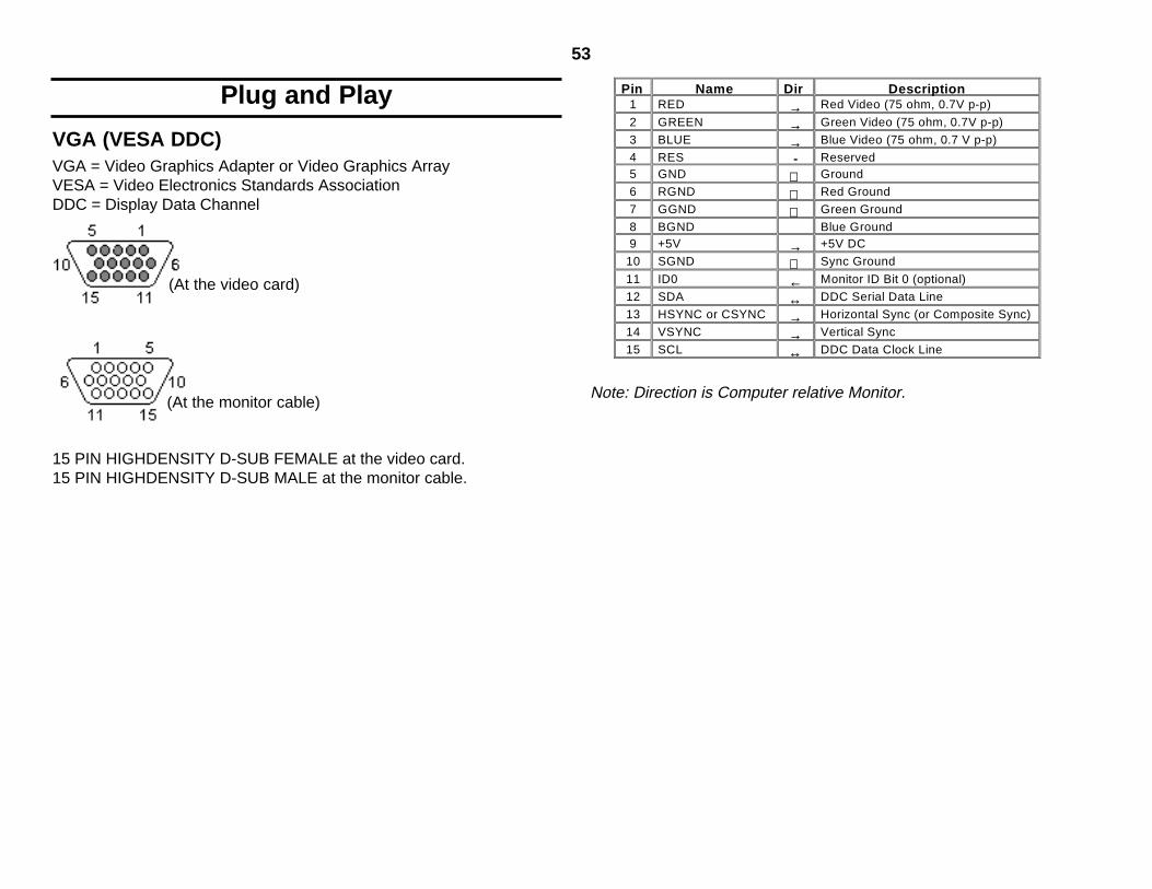
Plug and Play
VGA (VESA DDC)VGA = Video Graphics Adapter or Video Graphics ArrayVESA = Video Electronics Standards AssociationDDC = Display Data Channel
(At the video card)
(At the monitor cable)
15 PIN HIGHDENSITY D-SUB FEMALE at the video card.15 PIN HIGHDENSITY D-SUB MALE at the monitor cable.
Pin Name Dir Description1 RED → Red Video (75 ohm, 0.7V p-p)
2 GREEN → Green Video (75 ohm, 0.7V p-p)
3 BLUE → Blue Video (75 ohm, 0.7 V p-p)
4 RES - Reserved5 GND Ground
6 RGND Red Ground
7 GGND Green Ground
8 BGND Blue Ground9 +5V → +5V DC
10 SGND Sync Ground
11 ID0 ← Monitor ID Bit 0 (optional)
12 SDA ↔ DDC Serial Data Line
13 HSYNC or CSYNC → Horizontal Sync (or Composite Sync)
14 VSYNC → Vertical Sync
15 SCL ↔ DDC Data Clock Line
Note: Direction is Computer relative Monitor.

54
What is Plug and PlayCurrently there are several levels of Plug and Play compliance. DDC1(Display Data Channel 1) capable monitors can communicate with thedisplay adapter in only one direction through an unused line on the stan-dard VGA cable. The DDC1 type of communication is the type of datachannel from the display to the host, continuously transmitting ExtendedDisplay Identification (EDID) information. The video adapter is told whatmonitor is connected and its maximum resolutions and refresh rates.
DDC2B goes one step further by offering bi-directional communicationsthrough two unused VGA lines between the monitor and the video adapter.The DDC2B communication channel is based on the I2C protocol. Thehost (graphics card) can request EDID or VDIF (Video Information) infor-mation over the DDC2B channel. Not only is DDC2B faster, it allows theoperating system to query the monitor for supported features and informyou of any configuration changes. For your monitor to be fully Plug andPlay compatible, it must have both DDC1 and DDC2B capabilities. Witha Plug and Play video adapter, you are able to change resolutions andcolors without having to restart your computer.
Designers are developing innovations to keep pace with Plug and Play,such as a communication cable that plugs into a port similar to a tele-phone jack on the monitor. With the introduction of the ACCESS.bus (orDDC2AB compatibility), include DDC2B bi-directional communication andto add connectivity between many devices. ACCESS.bus peripheralscan be daisy chained in any order so that everything plugs into one porton the back of your computer system.
Since the ACCESS.bus conveys information directly to your system, miceand keyboards as well as other compatible components can be pluggedand unplugged without having to restart your computer. Especially usefulfor monitors, the ACCESS.bus allows you to adjust your screens imageusing a mouse and keyboard. This not only eliminates the need to pushbuttons on the display, it allows you to store monitor settings under mean-ingful names that are easily recalled.
The newest standard, USB (Universal Serial Bus), includes all the capa-bilities of ACCESS.bus, but transmits and receives data at a much fasterrate. Instead of 400K/sec., USB will be able to communicate at an incred-ibly fast 12MB of data per second, which makes it ideal for digital videoand telephony. Because of its transmission capabilities, USB is expectedto win over the current ACCESS.bus standard and will be the one to watchas Plug and Play continues to mature.

55
Display Data Channel Circuit
DDC1The front input supports DDC1 communications. The front input cable pin12 (SDA) and pin 15 (SCL) are connected to CN312 pin 1 (DDCSCL) andpin 2 (DDCSDA) on the A Board. IC007 EEPROM pin 5 (SDA) and pin 6(SCL) provides the host with DDC1 communication. The V Sync input toIC007/7 (VCLK) is used to synchronize the timing of the data readingcycle.
IC007/7 VCLK
DDC2B and DDC2ABThe rear input supports DDC2B and DDC2AB communications. The rearinput cable pin 12 (SDA) and pin 15 (SCL) are connected to CN310 pin 2(DDCSCL) and pin 3 (DDCSDA) on the A Board. The data is passedthrough the A Board to CN311 pin 2 (DDCSCL) and pin 3 (DDCSDA).CN311 is connected to the N Board via connector CN1003 pin 2 (DDCCLK)and pin 3 (DDCDATA) and are input to IC1001 pin 34 (DDCCLK) and pin35 (DDCDATA).
CN311/3 DDCSDA

56

57
DDC Data Format (EDID)
Basic EDID consist of 128 bytesNumber Description8 Bytes Header10 Bytes Vendor / Product Identification2 Bytes EDID Version / Revision5 Bytes Basic Display Parameters / Features10 Bytes Color Characteristics3 Bytes Established Timings16 Bytes Standard Timings72 Bytes Detailed Timing Description1 Byte Extension Flag1 Byte Checksum

58
NOTES

59
Horizontal Deflection
OverviewThe Micro IC1001 and DSP IC1002 (N Board) respond to the Timing andSync parameters of the video inputs and provide the necessary Horizon-tal Drive and Geometric correction waveforms for the Horizontal Deflec-tion circuit on the D Board. Horizontal Deflection and High Voltage iscontrolled by IC805 HV / H SIZE REG CTRL. IC805 produces PWM(Pulse Width Modulation) drive outputs to control for Size, Bow, Pincush-ion and Keystone. Control for linearity, centering and impedance match-ing are also part of the Horizontal Deflection circuit.
Horizontal DriveIC1002 (N Board) outputs Horizontal Drive on pin 25 (H-OUT) via CN101/26 to CN801/26 (HD OUT) on the D Board. The HD OUT signal is appliedto Q501 H Drive buffer. Q501 shapes, amplifies and inverts the HD OUTsignal and is applied to Q502 and Q503 Push-Pull H Drive buffer. Q502and Q503 amplify the HD OUT signal and is applied to Q504 H Drive.The -16V DC supply is applied to Q504/S and the Drain of Q504 is at 0VDC via T501 to ground. Q504 drives T501 HDT (Horizontal Drive Trans-former) which provides base current to Q505 H OUT. Q505 collectorproduces approximately 1kV P-P spike to drive the positive side of theHorizontal Deflection Yoke (H DY+) through T504 HST (Horizontal SizeTransformer). The negative side of the Horizontal Deflection Yoke (HDY-) is AC coupled to ground via L502 HLC (Horizontal Linearity Coil),T503 LCT (Linearity Coil Transformer), L505, R522 and C513.
CN801/26 HD OUT
Q505/C

60

61
Horizontal AFCThe horizontal output pulse of Q505 H OUT is coupled to Q514 H RTRCand buffered. The horizontal pulse H FBP via CN801/ 32 to CN1001/2 (NBoard) is input to IC1002/27 (FBP-IN). IC1002 utilizes the H FBP to phaselock the HD OUT signal at pin 25 (HD OUT).
CN801/32 H. FBP

62

63
Horizontal Size ControlThe HD OUT signal from Q502 and Q503 Push-Pull H Drive buffer is alsoinput to IC805/8. IC805 utilizes the HD OUT signal to produce the properPWM output frequency at pin 20. The DSP IC1002/64 (E/W) output throughCN1001/27 to CN801/27 (H.SHAPE) is input to IC805/2. The H.SHAPEparabola waveform is utilized by IC805 to control the H SIZE by alteringthe duty cycle of the PWM drive output at pin 20. The PWM output isapplied to Q506 H SIZE REG OUT. Q506 controls the amount of B+(approximately +70V) through T502 HOC (Horizontal Output Coil) that isapplied to Q505 H OUT to adjust for correct screen (raster) size. T504HST (Horizontal Size Transformer) is utilized to sense the deflection cur-rent through the H DY. The voltage on the secondary of T504 is rectifiedby D508 and buffered by Q518 and is input to IC805/3. IC805 utilizes thisfeedback input voltage to mix with the H.SHAPE waveform to maintainand control correct screen (raster) size.
IC805/2 H.SHAPE
IC805/3 Size Feedback
IC805/20 PWM

64

65
Pin, Keystone, Bow and Geometric CorrectionsThe DSP IC1002 (N Board) pin 64 (E/W) output is also used for Pin,Keystone, Bow and Geometric corrections. IC1002 alters the parabolawaveform (H.SHAPE) that is input to IC805/2. IC805/20 outputs the nec-essary PWM drive to Q506 H SIZE REG OUT to control the amount of B+that is applied to Q505 H OUT. By adjusting the amount of B+, the circuitcan correct for Pin, Keystone and Bow.
IC805/2 H. SHAPE
IC805/20 PWM

66

67
Horizontal Centering ( Raster only )The Micro IC1001 (N Board) controls the Raster position via the Horizon-tal Centering circuit comprised of Q517, Q515 and IC502 (H CENT OUT).The Horizontal Centering (Raster only) can only be adjusted using theDAS Software. IC1001 outputs Horizontal Centering voltage on pin 4 viaCN1001/30 to CN801/30 (H.CENT) on the D Board. The H.CENT volt-age is applied to Q517 buffer and is then applied to Q515 H CTR CTRL.Q515 inverts and amplifies the H.CENT voltage and is input to IC502/2 (-). When Horizontal Centering is adjusted, the voltage input to IC502/2 (-) varies and as a result the output of IC502/4 (O) also varies. The outputof IC502/4 (O) via R541, R546 and L503 applies a positive or negativeDC offset to the Drain of Q506 H SIZE REG OUT. This DC offset movesthe Raster position left or right of center. Q802 and Q516 are controlledby the ‘REMOTE ON/OFF’ command to mute the input to IC502 duringpower save.
Caution: IC502 is powered by a floating supply. Do not attempt to checkvoltages at IC502 with an O-Scope by attaching a ground lead to T601/17(floating ground). This may result in damage to IC502. Use a DVM whenverifying voltages around IC502.

68

69
Horizontal LinearityThe Micro IC1001/2 (N Board) outputs Horizontal Linearity control viaCN1001/28 to CN801/28 (H. LIN BAL) on the D Board. The HorizontalLinearity circuit is comprised of L502 HLC (Horizontal Linearity Coil), T503LCT (Linearity Coil Transformer) and Q507 HLC CTRL. Horizontal Lin-earity can only be adjusted using the DAS Software. The H. LIN BALcontrol is applied to Q507. L502 HLC and the primary of T503 LCT are inparallel. The secondary of T503 is controlled by the conduction of Q507,which varies the voltage across the winding. This voltage across thesecondary winding changes the inductance of the primary winding of T503.Therefore, the Horizontal Linearity is controlled by varying the primaryinductance of T503. Horizontal Linearity is also maintained through eachof the Timing and Sync parameters of the video inputs.

70

71
Impedance Matching (S CAPS)The Micro IC1001 (N Board) controls the Impedance Matching (S CAPS)circuit to match the Timing and Sync parameters of the video inputs. TheS CAPS are utilized to switch different capacitors into the horizontal de-flection yoke, thus changing the impedance. IC1001 pin 46 S5, pin 47S4, pin 48 S3, pin 49 S2, pin 50 S1 and pin 53 S0 control the S CAPcircuits comprised of circuit elements Q508, Q509, Q510, Q511, Q512,Q513 and associated components respectively. IC1001 outputs a H (+5V)to switch the respective S CAP into the circuit.
Note: With No Video Input, the H freq. Is 69.696kHz and the S Cap logicoutputs are all +5V.
S CAP TablesMicro IC1001 S CAP Switching No Sync Input DOS Prompt
Pin53
S0Q513
H+5V
H+5V
Pin50
S1Q512
H+5V
H+5V
Pin49
S2Q511
H+5V
H+5V
Pin48
S3Q510
H+5V
L0V
Pin47
S4Q509
H+5V
H+5V
Pin46
S5Q508
H+5V
H+5V
N Board H Freq. 69.696 kHz 31.496 kHz
Picture resolutions were generated using Windows 95 “Display Properties” for the CPD-420GS.
Resolution (Dots x Lines)S CAP Switching 640 X 480 800 X 600 1024 X 768 1152 X 864 1280 X 1024 1600 X 1200
S0Q513
H+5V
H+5V
H+5V
H+5V
L0V
H+5V
S1Q512
H+5V
H+5V
H+5V
H+5V
H+5V
L0V
S2Q511
L0V
H+5V
H+5V
H+5V
L0V
H+5V
S3Q510
H+5V
H+5V
L0V
L0V
L0V
L0V
S4Q509
H+5V
L0V
L0V
L0V
L0V
L0V
S5Q508
L0V
L0V
L0V
L0V
L0V
L0V
H Freq. 43.284 kHz 53.545 kHz 68.740 kHz 67.523 kHz 90.894 kHz 74.268 kHz

72

73
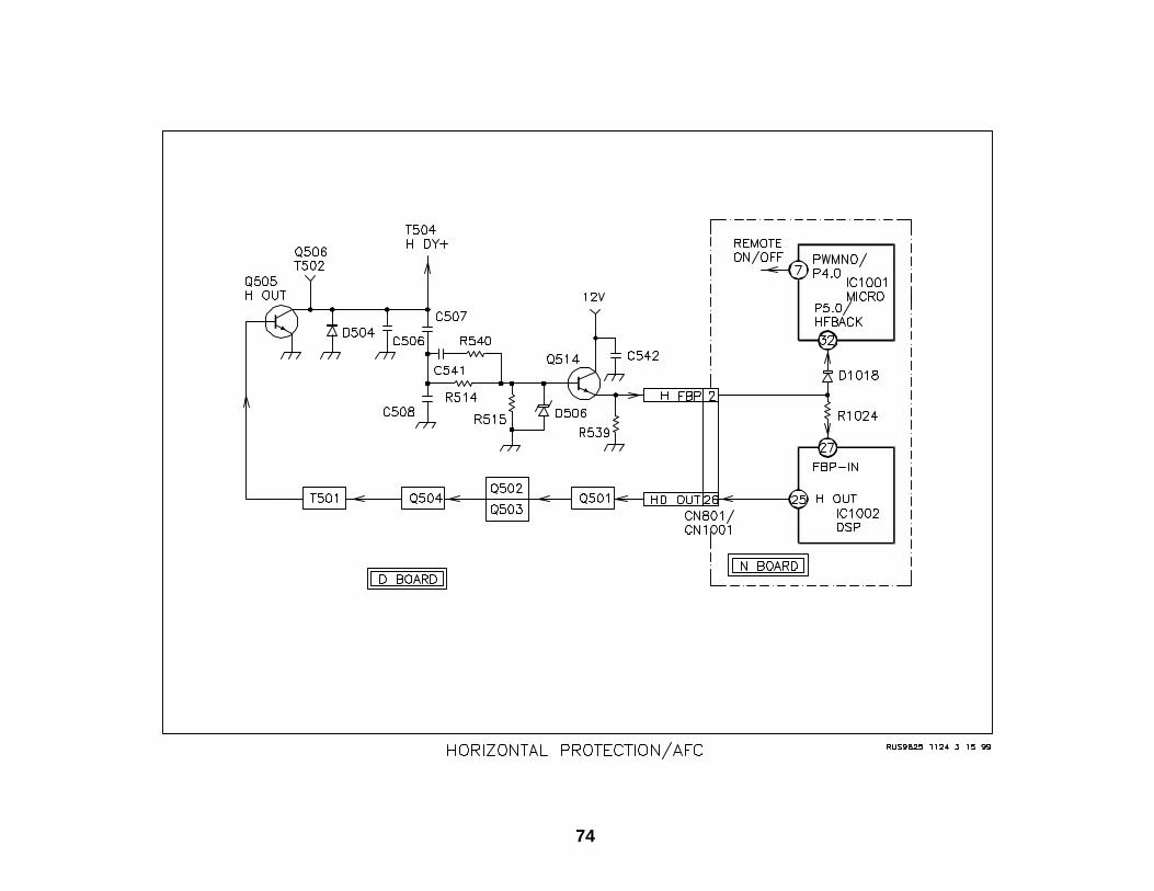
Horizontal Deflection Shutdown
ProtectionThe horizontal output pulse of Q505 H OUT is coupled to Q514 (H RTRC)and buffered. The buffered horizontal pulses H FBP via CN801/32 toCN1001/2 (N Board) is input to IC1002/27 (FBP-IN). IC1002 utilizes theH FBP to phase lock the HD OUT signal at pin 25 (HD OUT). The H FBPsignal is also input to IC1001/32. IC1001 monitors the H FBP pulses andif the pulses are missing, IC1001/7 ‘REMOTE ON/OFF’ goes L (0V) to setthe power supply in the ‘Active Off’ mode.
CN801/32 H.FBP
NOTE: LED illuminates Orange (1.5 seconds) / Off (0.5 seconds).
74

75
High Voltage CircuitOverviewThe HV (High Voltage) circuit is comprised of circuit elements IC805 (HV/ H SIZE REG CTRL), Q901 (HV REG OUT), Q902 (HV OUT) and T901(FBT). These circuits develop regulated CRT Anode voltage, G2 (Screen)voltage and Focus voltage. In addition, there are High Voltage and BeamCurrent protection circuits.
High VoltageIC805 (HV / H SIZE REG CTRL), utilizes the HD OUT input signal at pin8 to produce the proper HV Drive PWM output frequency at pin 19. TheHV Drive PWM is applied to Q902 (HV OUT), which produces approxi-mately 700V P-P pulses and drives the input of T901 (FBT). The second-ary of T901 internally rectifies the pulses and generates the necessaryHV for the CRT Anode.
IC805/19 PWM
High Voltage RegulationA sample of the HV produced by T901 is output at pin 17. This voltage isdivided by (R810, R902, R903, R906, R907, R923 and RV904) and inputto IC805/12. This sampled feedback voltage is mixed with the internaltriangle OSC and output as PWM drive at pin 18. The PWM correctiondrive output is applied to Q901 (HV REG OUT) which controls the amountof B+ (approximately +48V) applied through T902 HRC to Q902 to main-tain and regulate the HV. The feedback voltage is inversely proportionalto the B+ that is applied to Q902.RV904 is incorporated into the HV voltage divider network to set the HVlevel produced. RV904 varies the HV sampled feedback voltage to IC805/12.
IC805/19 PWM
G2 (Screen) VoltageThe G2 Screen voltage is produced by T901/8 FBT via R917 and rectifiedby D905 to produce the 1000V DC. The G2 voltage is then routed viaCN510 to the A Board to the G2 control circuit.

76

77
ABL (Auto Brightness Limiting)The ABL circuit is used to control the overall beam current and brightnessof the CRT. The T901/11 FBT output is rectified by D904 and filtered byC929. As beam current increases, the voltage output from T901/11 de-creases (current is inversely proportional to the voltage). This voltage viaD802 and D801 is input to IC805/13 (REF). When beam current be-comes excessive and the output voltage from T901/11 decreases, thereference voltage at IC805 pin 13 and pin 14 is decreased. As a result,the duty cycle of the PWM output from IC805/18 is reduced and the HVoutput is decreased to limit beam current and prevent CRT damage.
IC805/18 PWM

78

79
HV Protection
HV ShutdownHigh Voltage protection is performed by monitoring the +300V DC outputsource from T901/8 FBT via R917 and rectifier D905. The +300V DCsource is voltage divided by R921 and R922. When the HV rises abovethe threshold of D908, the HV DET line of IC1001/16 will rises above +5VDC. This results in IC1001/7 ‘REMOTE ON/OFF’ to go L (0V) causing thepower supply to enter the ‘Active Off’ mode.
NOTE: If HV becomes excessive, LED illuminates Orange (0.5 seconds)/ Off (0.5 seconds).
ABL ShutdownABL Shutdown is activated when CRT beam current becomes excessive.T901/11 FBT output is rectified by D904 and filtered by C929. As beamcurrent increases, the voltage output from T901/11 decreases (current isinversely proportional to the voltage). In extreme cases when beam cur-rent becomes excessive and the output voltage from T901/11 decreasesto 0V, IC1001/7 ‘REMOTE ON/OFF’ responds by going L (0V) and as aresult, the power supply enters the ‘Active Off’ mode.
NOTE: If Beam current (ABL) becomes excessive, LED illuminates Or-ange (0.5 seconds) / Off (1.5 seconds).

80

81
Dynamic Focus (DF) CircuitOverviewTwo separate Dynamic Focus circuits (Horizontal and Vertical) are incor-porated to provide an increase in the overall sharpness of the picture,especially in the corners of the CRT. Each of these circuits provide theirown respective correction waveform. Previous chassis designs used asingle correction waveform to create Dynamic Focus control.
Horizontal DFThe Horizontal Dynamic Focus circuit is comprised of circuit elementsIC703 (H DF OUT) and T701 (DFT). IC1002 DSP (N Board) pin 10 (HDF1)outputs the H.DF correction waveform and is input to IC703/4 (+IN A).The output of IC703/6 (OUT A) drives the primary of T701 DFT. T701secondary steps up the HDF waveform and via R908 and is applied to theFocus voltage at T901/14 FBT.
IC703/4 H.DF
IC703/6 H.DF OUT

82

83
Vertical DFThe Vertical Dynamic Focus circuit is comprised of circuit elements Q706and Q707. IC1002 DSP (N BOARD) pin 58 (VDF1) outputs the V.DFcorrection waveform and is applied to Q707, buffered and applied to Q706.Q706 inverts and amplifies the V.DF waveform and via R909 is applied tothe Focus voltage at T901/15 FBT.
NOTE: IC703/11 (STBY) is controlled by the ‘REMOTE ON/OFF’ logic todisable the outputs of IC703 in the ‘Active Off’ and ‘Standby/Suspend’modes.
NOTE: T901 FBT has two Focus controls that can be individually ad-justed to perform overall Horizontal and Vertical Focus respectively.
Q707/B V.DF
Q706/C V.DF

84

85
Vertical Deflection
Vertical DriveThe DSP IC1002 (N Board) pin 1 (VSAWN) outputs the vertical sawtoothwaveform signal. The vertical sawtooth waveform is buffered by IC1007(1/2) and is routed to the D Board. The vertical sawtooth waveform isthen input to IC401/7 (V IN). IC401 current amplifies the vertical sawtoothwaveform and outputs drive at pin 5 to the Vertical Deflection Yoke viaCN501/6. IC1002/2 (DCC2) provides a DC reference voltage via IC1007(2/2) buffer and is applied to IC401/1.
CN801/13 VSAWN
IC401/5 V DRIVE
Vertical Geometric CorrectionsVertical Geometric Corrections can only be performed via the DASSoftware. Vertical Size and Centering are the only adjustmentsthat can be accessed by the user via the OSD menu. The MicroIC1001 via the I2C bus communicates with the DSP IC1002. IC1002/1 (V SAWN) outputs the necessary vertical sawtooth waveform toIC401 to be applied to the Vertical Deflection Yoke.
CN801/13 VSAWN
· The V SAWN waveform controls the Vertical Size by varying the am-plitude.
· The V SAWN waveform controls the Vertical Linearity by varying theshape.

86

87
Vertical CenteringVertical Centering is performed by varying the DC offset of the V SAWNwaveform in respects to the DCC2 reference voltage. The DC shift isproportional to the direction of the raster. As the DC shift is more positive,the raster is moved upwards and as the DC shift is made less positive, theraster is moved downwards.
CN801/13 VSAWN
· Remember the V SAWN waveform controls the Vertical Centering byvarying the DC Offset with respects to the DCC2 reference voltage.
Vertical Feedback PulseThe vertical flyback pulse from IC401/3 through R407 is rectified by D405and filtered by C409. The DC voltage (V.FBP) is routed to the N Board toIC1002/39 (V-FBK). IC1002 monitors the DC voltage to confirm that Ver-tical Deflection is operating. When the DC voltage is 0V, IC1002/40 (BLK)disables the blanking pulse to the A Board to mute the video.

88

89
Vertical Protection
Vertical ProtectionThe vertical flyback pulse from IC401/3 through R407 is rectified by D405and filtered by C409. The DC voltage (V.FBP) is routed to the N Board toMicro IC1001/42. IC1001 monitors the DC voltage to confirm that Verti-cal Deflection is operating. When the DC voltage reaches 0V, IC1001/7‘REMOTE ON/OFF’ goes L (0V) to set the power supply in the ‘Active Off’mode.
NOTE: LED illuminates Orange (1.5 seconds) / Off (0.5 seconds)

90

91
Rotation and Vertical Key Circuits
RotationRotation adjustments can be made via the user OSD menu and via theDAS Software. The Micro IC1001/3 (N Board) outputs the ‘ROTATION’PWM control waveform and is routed to the D Board. The PWM wave-form is filtered by R729 and C705 and the DC level is applied to IC702/2(-). IC702 current amplifies the DC level and the output at pin 4 (O) drivesthe Rotation Coil via CN702. When the Rotation adjustment is performed,the PWM duty cycle changes which results in a change of the DC levelapplied to IC702/2 (-). The output of IC702/4 (O) varies from approxi-mately +11V DC to -11V DC. The input to IC702/1 (+) is set to a DCreference source.
· The ‘ROTATION’ PWM waveform controls the Rotation by varyingthe duty cycle of the waveform.
Vertical KeyThe Vertical Key adjustment can only be performed via the DAS Soft-ware. The DSP IC1002/59 (VDF2) outputs the ‘D.TILT’ triangle wave-form and is routed to the D Board. The D.TILT waveform via R736 isapplied to the DC reference source, which is input to IC702/1 (+). Whenthe Vertical Key adjustment is performed, the D.TILT triangle waveformvaries in shape and as a result the DC reference source is varied by theD.TILT waveform.
· The D.TILT waveform controls the Vertical Key by varying the shapeof the waveform.

92

93
Convergence Circuits
OverviewThe Static Convergence adjustments can be performed by the DAS Soft-ware or the user OSD menu. The Dynamic Convergence adjustmentscan only be performed using the DAS Software. The DSP IC1002 (NBoard) provides the Static Convergence IC704 (S CONV OUT) and theDynamic Convergence IC701 (D CONV OUT) with the complex two-di-mensional convergence waveforms and DC bias. The Static Conver-gence circuit provides correction for the R G B beam landing in the centerareas of the CRT. And the Dynamic Convergence circuit provides correc-tion for the R G B beam landing in the outer areas of the CRT via aseparate convergence yoke on the CRT.
Static Convergence IC704The DSP IC1002/60 (YSC) outputs the complex convergence waveformand is routed to the D Board. The YSC signal is input to IC704/7 (INB-).IC704 current amplifies the YSC signal and the output at pin 9 (IOUTB) isapplied to the convergence yoke. When the Static Convergence adjust-ment is performed, IC1002 varies the DC reference level of the YSC sig-nal positive or negative. The YSC signal is applied to the convergenceyoke to shift the R and B beam landing in the horizontal direction.
IC704/7 YSC
The DSP IC1002/61 (XSC) outputs the complex convergence waveformand is routed to the D Board. The XSC signal is input to IC704/3 (INA-).IC704 current amplifies the XSC signal and the output at pin 1 (IOUTA) isapplied to the convergence yoke. When the Static Convergence adjust-ment is performed, IC1002 varies the DC reference level of the XSC sig-nal positive or negative. The XSC signal is applied to the convergenceyoke to shift the R and B beam landing in the vertical direction.
IC704/3 XSC
The voltage divider network on the N Board comprised of circuit elementsR1102, R1103 and R1007 is routed to the D Board to provide IC704 pin 4(INA+) and pin 6 (INB+) with a DC bias voltage offset (DAC REF).

94

95
Dynamic Convergence IC701The DSP IC1002/8 (YDC) outputs the complex convergence waveformand is routed to the D Board. The YDC signal is input to IC701/2 (+IN B).IC701 current amplifies the YDC signal and the output at pin 1 (OUT B) isapplied to the convergence yoke. When the Dynamic Convergence ad-justment is performed, IC1002 varies the DC reference level, shape andsize of the YDC signal. The YSC signal is applied to the convergenceyoke to shift the R and B beam landing in the horizontal direction in theouter areas of the CRT.
IC701/2 YDC
The DSP IC1002/6 (XDC) outputs the complex convergence waveformand is routed to the D Board. The XDC signal is input to IC701/5 (-IN A).IC701 current amplifies the XDC signal and the output at pin 6 (OUT A) isapplied to the convergence yoke. When the Dynamic Convergence ad-justment is performed, IC1002 varies the DC reference level, shape andsize of the XDC signal. The XDC signal is applied to the convergenceyoke to shift the R and B beam landing in the vertical direction in the outerareas of the CRT.
IC701/6 XDC
The DSP IC1002/7 (DCC) output is routed to the D Board to provide IC701pin 3 (+IN B) and pin 4 (+IN A) with a DC bias voltage offset (REF DC).
The Micro IC1001/7 ‘REMOTE ON/OFF’ output is routed to the D Boardand is input to IC701/11 (STBY) to mute the outputs of IC701 when in the‘Active Off’ and ‘Standby/Suspend’ modes.

96