Embed Size (px)
Citation preview
DS-7315 Rev 05 2016-12-12
SPG-FE-FX-IDFC SPG-FE-FX-CDFC
Features
Built-in PHY supporting SGMII Interface
Built-in high performance MCU supporting easier
configuration
Support more link status monitor, such as CRC error
counter, package counter
100BASE-FX operation
1310nm FP laser and PIN photo-detector
Up to 2km transmission with MMF
Standard serial ID information Compatible with SFP MSA
SFP MSA package with duplex LC connector
With Spring-Latch for high density application
+3.3V single power supply
Operating case temperature:
I-temp: -40 to +85°C; C-temp:-5 to 70°C
Regulatory Compliance
Table 1 - Regulatory Compliance
Feature Standard Performance
Electrostatic Discharge
(ESD) to the Electrical Pins
MIL-STD-883E
Method 3015.7 Class 1
Electrostatic Discharge (ESD) to the
Duplex LC Receptacle
IEC 61000-4-2
GR-1089-CORE Compatible with standards
Electromagnetic
Interference (EMI) FCC Part 15 Class B Compatible with standards
Laser Eye Safety FDA 21CFR 1040.10 and 1040.11
EN (IEC) 60825-1,2
Compatible with Class I laser
product.
RoHS 2011/65/EU Compliant with RoHS
Absolute Maximum Ratings
Table 2 - Absolute Maximum Ratings
Parameter Symbol Min. Typical Max. Unit Notes
Storage Temperature TS -40 - +85 °C
Supply Voltage VCC -0.5 - +3.6 V
Operating Relative Humidity RH 5 - +95 %
Power consumption 1.2 W
DS-7315 Rev 05 2016-12-12
SPG-FE-FX-IDFC SPG-FE-FX-CDFC
Recommended Operating Conditions
Table 3 – Recommended Operating Conditions
Parameter Symbol Min. Typical Max. Unit Notes
Operating Case
Temperature
I-temp TC -40 - +85 °C
C-temp TC -5 - +70 °C
Power Supply Voltage VCC 3.10 3.3 3.50 V
Power Supply Current ICC - - 350 mA 1
Date Rate 125 Mbps
Note 1: The max. power supply current after module work stable.
Optical Characteristics
Table 4 – Optical Characteristics
Transmitter
Parameter Symbol Min. Typical Max. Unit Notes
Centre Wavelength λC 1260 1310 1360 nm
Average Output Power P0ut -20 -14 dBm 1
P0ut@TX Disable Asserted P0ut -45 dBm 1
Spectral Width (RMS) 7.7 nm
Extinction Ratio EX 9 dB
Rise/Fall Time (20%~80%) tr/tf 3 ns 2
Output Optical Eye Compatible with IEEE 802.3-2002 3
Receiver
Centre Wavelength λC 1260 1310 1570 nm
Receiver Sensitivity -31.5 dBm 4
Receiver Overload -8 dBm 4
Return Loss 12 dB
LOS De-Assert LOSD -32.5 dBm
LOS Assert LOSA -45 dBm
LOS Hysteresis 0.5 4.5 dB
Total Jitter
(SGMII Series Interface) TJ 0.43 UI
Notes:
1. The optical power is launched into 62.5/125um MMF.
2. Unfiltered, measured with 4B/5B code for 125Mbps
3. Measured with 4B/5B code for 125Mbps.
DS-7315 Rev 05 2016-12-12
SPG-FE-FX-IDFC SPG-FE-FX-CDFC
4. Measured with 4B/5B code for 125Mbps, worst-case extinction ratio, and BER ≤1 × 10⁻¹⁰.
Electrical Characteristics
Table 5 – Electrical Characteristics
Transmitter
Parameter Symbol Min. Typical Max. Unit Notes
Data Input Swing Differential
(SGMII Series interface) VIN 200 2100 mV 1
Input Differential Impedance ZIN 80 100 120 Ω
TX Disable Disable 2.0 Vcc
V
Enable Vee Vee+0.8
TX Fault Fault 2.0 Vcc
V
Normal Vee Vee+0.5
Receiver
Data Output Swing Differential
(SGMII Series Interface) VOUT 370 2000 mV 1
LOS High 2.0 Vcc+0.3
V
Low Vee Vee+0.5
Notes:
1. PECL logic, internally AC coupled.
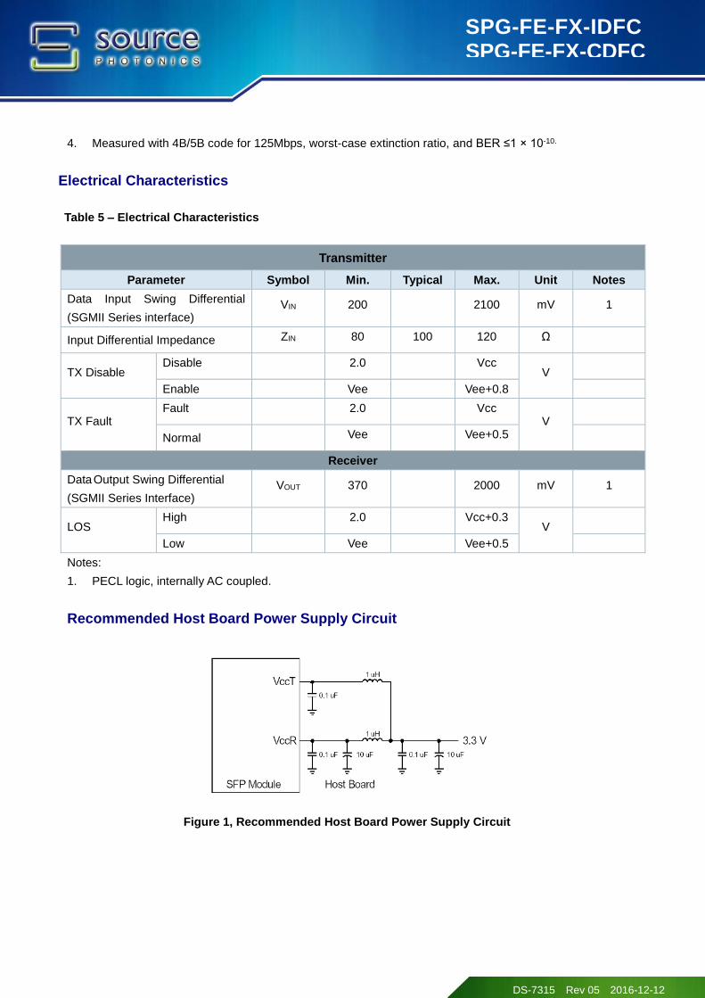
Recommended Host Board Power Supply Circuit
Figure 1, Recommended Host Board Power Supply Circuit
DS-7315 Rev 05 2016-12-12
SPG-FE-FX-IDFC SPG-FE-FX-CDFC
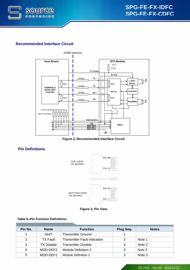
Recommended Interface Circuit
Figure 2, Recommended Interface Circuit
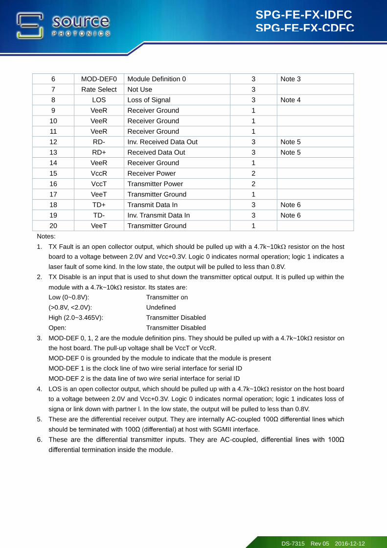
Pin Definitions
Pin 10
Pin 1
Pin 11
Pin 20
BOTTOM VIEW
OF BOARD
OF BOARD
TOP VIEW
Figure 3, Pin View
Table 6–Pin Function Definitions
Pin No. Name Function Plug Seq. Notes
1 VeeT Transmitter Ground 1
2 TX Fault Transmitter Fault Indication 3 Note 1
3 TX Disable Transmitter Disable 3 Note 2
4 MOD-DEF2 Module Definition 2 3 Note 3
5 MOD-DEF1 Module Definition 1 3 Note 3
DS-7315 Rev 05 2016-12-12
SPG-FE-FX-IDFC SPG-FE-FX-CDFC
6 MOD-DEF0 Module Definition 0 3 Note 3
7 Rate Select Not Use 3
8 LOS Loss of Signal 3 Note 4
9 VeeR Receiver Ground 1
10 VeeR Receiver Ground 1
11 VeeR Receiver Ground 1
12 RD- Inv. Received Data Out 3 Note 5
13 RD+ Received Data Out 3 Note 5
14 VeeR Receiver Ground 1
15 VccR Receiver Power 2
16 VccT Transmitter Power 2
17 VeeT Transmitter Ground 1
18 TD+ Transmit Data In 3 Note 6
19 TD- Inv. Transmit Data In 3 Note 6
20 VeeT Transmitter Ground 1
Notes:
1. TX Fault is an open collector output, which should be pulled up with a 4.7k~10k resistor on the host
board to a voltage between 2.0V and Vcc+0.3V. Logic 0 indicates normal operation; logic 1 indicates a
laser fault of some kind. In the low state, the output will be pulled to less than 0.8V.
2. TX Disable is an input that is used to shut down the transmitter optical output. It is pulled up within the
module with a 4.7k~10k resistor. Its states are:
Low (0~0.8V): Transmitter on
(>0.8V, <2.0V): Undefined
High (2.0~3.465V): Transmitter Disabled
Open: Transmitter Disabled
3. MOD-DEF 0, 1, 2 are the module definition pins. They should be pulled up with a 4.7k~10k resistor on
the host board. The pull-up voltage shall be VccT or VccR.
MOD-DEF 0 is grounded by the module to indicate that the module is present
MOD-DEF 1 is the clock line of two wire serial interface for serial ID
MOD-DEF 2 is the data line of two wire serial interface for serial ID
4. LOS is an open collector output, which should be pulled up with a 4.7k~10k resistor on the host board
to a voltage between 2.0V and Vcc+0.3V. Logic 0 indicates normal operation; logic 1 indicates loss of
signa or link down with partner l. In the low state, the output will be pulled to less than 0.8V.
5. These are the differential receiver output. They are internally AC-coupled 100Ω differential lines which
should be terminated with 100Ω (differential) at host with SGMII interface.
6. These are the differential transmitter inputs. They are AC-coupled, differential lines with 100Ω
differential termination inside the module.
DS-7315 Rev 05 2016-12-12
SPG-FE-FX-IDFC SPG-FE-FX-CDFC
EPROM Information
Table 7 –EEPROM Serial ID Memory Contents (A0h)
Addr. Field Size
(Bytes) Name of Field Hex Description
0 1 Identifier 03 SFP
1 1 Ext. Identifier 04 MOD4
2 1 Connector 07 LC
3—10 8 Transceiver 00 00 00 20 00 00 00 00 100BASE-FX
11 1 Encoding 02 4B5B
12 1 BR, nominal 01 125Mbps
13 1 Reserved 00
14 1 Length (9um)-km 00
15 1 Length (9um) 00
16 1 Length (50um) C8 2km
17 1 Length (62.5um) C8 2km
18 1 Length (copper) 00
19 1 Reserved 00
20—35 16 Vendor name 53 4F 55 52 43 45 50 48
4F 54 4F 4E 49 43 53 20 “SOURCEPHOTONICS “(ASCⅡ)
36 1 Reserved 00
37—39 3 Vendor OUI 00 1F 22
40—55 16 Vendor PN 53 50 47 46 45 46 58 xx
44 46 43 20 20 20 20 20
“SPGFEFXIDFC”
“SPGFEFXCDFC” (ASCⅡ)
56—59 4 Vendor rev 31 30 20 20 ASCⅡ( “31 30 20 20” means 1.0 revision)
60-61 2 Wavelength 05 1E 1310nm
62 1 Reserved 00
63 1 CC BASE xx Check sum of bytes 0 - 62
64—65 2 Options 00 1A LOS, TX_FAULT and TX_DISABLE
66 1 BR, max 00
67 1 BR, min 00
68—83 16 Vendor SN xx xx xx xx xx xx xx xx
xx xx xx xx xx xx xx xx ASCⅡ.
84—91 8 Vendor date code xx xx xx xx xx xx 20 20 Year (2 bytes), Month (2 bytes), Day (2 bytes)
92 1 Reserved 68
93 1 Reserved B0
94 1 Reserved 02
95 1 CC_EXT xx Check sum of bytes 64 - 94
96—255 160 Vendor specific
DS-7315 Rev 05 2016-12-12
SPG-FE-FX-IDFC SPG-FE-FX-CDFC
Recommended Software configuration
How to configure auto-negotiation, loopback, work speed
The module can support auto-negotiation, loopback configuration.
Please refer the following steps to configure:
Step 1: Access the module at 0xA2 via two-wire serial interface.
Step 2: Configure 0x6Dh/6Eh (Byte 109~110) as below table. Addr.109 default is “5Fh”. Addr.110 default is
“00h”.
Addr. 109 Function “1” “0” Default Value
(BIN)
bit7 FEFI Status FEFI condition detected FEFI condition not
detected
‘0’
bit6 Fiber
Auto-Negotiation
Disable Enable ‘1’
Bit5 MAC
Auto-Negotiation
Disable Enable ‘0’
bit4 FEFI function Disable Enable ‘1’
bit3 CRC checker Disable/Reset Enable ‘1’
bit2 Fiber loop back Disable Enable ‘1’
bit1 MAC loop back Disable Enable ‘1’
bit0 Reserved Reserved Reserved ‘1’
Addr. 110 Function “1” “0” Default Value
(BIN)
bit7 TX Disable State TX-Disable TX-Enable ‘0’
bit6 TX-Disable TX-Disable TX-Enable ‘0’
Bit5~Bit4 Reserved Reserved Reserved ‘0’
Bit3 Work speed mode 1000Base 100Base ‘0’
Bit2 TX fault output
status
TX fault indication No fault ‘0’
Bit1 LOS pin output
status
LOS asserted
(Link down)
LOS de-asserted
(Link up)
‘0’
Bit0 Data Ready status Not ready Ready ‘0’
Notes: “1” is invalid for Bit 3 in address 110(work speed is only 100Base).
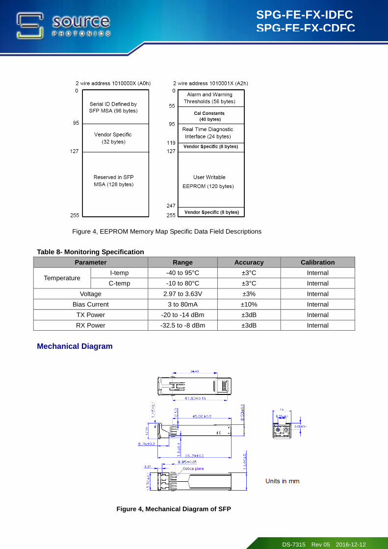
Monitoring Specification
The digital diagnostic monitoring interface also defines another 256-byte memory map in EEPROM,
which makes use of the 8 bit address 1010001X (A2h). Please see Figure 4. For detail EEPROM
information, please refer to the related document of SFF-8472 Rev 9.5. The monitoring specification of
this product is described in Table 8.
DS-7315 Rev 05 2016-12-12
SPG-FE-FX-IDFC SPG-FE-FX-CDFC
Figure 4, EEPROM Memory Map Specific Data Field Descriptions
Table 8- Monitoring Specification
Parameter Range Accuracy Calibration
Temperature I-temp -40 to 95°C ±3°C Internal
C-temp -10 to 80°C ±3°C Internal
Voltage 2.97 to 3.63V ±3% Internal
Bias Current 3 to 80mA ±10% Internal
TX Power -20 to -14 dBm ±3dB Internal
RX Power -32.5 to -8 dBm ±3dB Internal
Mechanical Diagram
Figure 4, Mechanical Diagram of SFP
DS-7315 Rev 05 2016-12-12
SPG-FE-FX-IDFC SPG-FE-FX-CDFC
Order Information
Table 8 – Order Information
Part No. Media Data Rate(Mbps) Transmission
Distance(km) Temperature
SPG-FE-FX-IDFC MMF 125 2 -40~+85°C
SPG-FE-FX-CDFC MMF 125 2 -5~+70°C

DS-7315 Rev 05 2016-12-12
SPG-FE-FX-IDFC SPG-FE-FX-CDFC
Warnings
Handling Precautions: This device is susceptible to damage as a result of electrostatic discharge (ESD).
A static free environment is highly recommended. Follow guidelines according to proper ESD procedures.
Laser Safety: Radiation emitted by laser devices can be dangerous to human eyes. Avoid eye exposure to
direct or indirect radiation.
Legal Notice
IMPORTANT NOTICE!
All information contained in this document is subject to change without notice, at Source Photonics’s sole
and absolute discretion. Source Photonics warrants performance of its products to current specifications
only in accordance with the company’s standard one-year warranty; however, specifications designated as
“preliminary” are given to describe components only, and Source Photonics expressly disclaims any and all
warranties for said products, including express, implied, and statutory warranties, warranties of
merchantability, fitness for a particular purpose, and non-infringement of proprietary rights. Please refer to
the company’s Terms and Conditions of Sale for further warranty information.
Source Photonics assumes no liability for applications assistance, customer product design, software
performance, or infringement of patents, services, or intellectual property described herein. No license,
either express or implied, is granted under any patent right, copyright, or intellectual property right, and
Source Photonics makes no representations or warranties that the product(s) described herein are free
from patent, copyright, or intellectual property rights. Products described in this document are NOT
intended for use in implantation or other life support applications where malfunction may result in injury or
death to persons. Source Photonics customers using or selling products for use in such applications do so
at their own risk and agree to fully defend and indemnify Source Photonics for any damages resulting from
such use or sale.
THE INFORMATION CONTAINED IN THIS DOCUMENT IS PROVIDED ON AN “AS IS” BASIS. Customer
agrees that Source Photonics is not liable for any actual, consequential, exemplary, or other damages
arising directly or indirectly from any use of the information contained in this document. Customer must
contact Source Photonics to obtain the latest version of this publication to verify, before placing any order,
that the information contained herein is current.