Embed Size (px)
Citation preview
PHYSICAL REVIEW B 90, 035142 (2014)
Spin and valley polarization of plasmons in silicene due to external fields
B. Van Duppen,1,* P. Vasilopoulos,2 and F. M. Peeters1
1Department of Physics, University of Antwerp, Groenenborgerlaan 171, B-2020 Antwerp, Belgium2Department of Physics, Concordia University, 7141 Sherbrooke Ouest Montreal, Quebec, Canada H4B 1R6
(Received 20 June 2014; revised manuscript received 8 July 2014; published 30 July 2014)
The electronic properties of the two-dimensional material silicene are strongly influenced by the applicationof a perpendicular electric field Ez and of an exchange field M due to adatoms positioned on the surfaceor a ferromagnetic substrate. Within the random phase approximation, we investigate how electron-electroninteractions are affected by these fields and present analytical and numerical results for the dispersion of plasmons,their lifetime, and their oscillator strength. We find that the combination of the fields Ez and M brings a spinand valley texture to the particle-hole excitation spectrum and allows the formation of spin- and valley-polarizedplasmons. When the Fermi level lies in the gap of one spin in one valley, the intraband region of the correspondingspectrum disappears. For zero Ez and finite M the spin symmetry is broken and spin polarization is possible. Thelifetime and oscillator strength of the plasmons are shown to depend strongly on the number of spin and valleytype electrons that form the electron-hole pairs.
DOI: 10.1103/PhysRevB.90.035142 PACS number(s): 73.20.Mf, 71.45.Gm, 71.10.−w
I. INTRODUCTION
Since its realization as a truly two-dimensional (2D)material, graphene has attracted much interest, both due tofundamental science and technological importance in variousfields [1]. However, the realization of a tunable band gap, suit-able for device fabrications, is still challenging and spin-orbitcoupling (SOC) is very weak in graphene. To overcome theselimitations researchers have been increasingly studying similarmaterials. One such material, called silicene, is a monolayerhoneycomb structure of silicon and has been predicted tobe stable [2]. Already several attempts have been made tosynthesize it [3–6] and its properties are reviewed in Ref. [7].
Despite controversy over whether silicene has been createdor not [8], it is expected to be an excellent candidate materialbecause it has a strong SOC and an electrically tunableband gap [9–11]. It’s a single layer of silicon atoms with ahoneycomb lattice structure and compatible with silicon-basedelectronics that dominates the semiconductor industry. Sil-icene has Dirac cones similar to those of graphene and densityfunctional calculations showed that the SOC induced gap init is about 1.55 meV [9,10]. Moreover, very recent theoreticalstudies predict the stability of silicene on nonmetallic surfacessuch as graphene [12], boron nitride, or SiC [13], and ingraphene-silicene-graphene structures [14]. Besides the strongSOC, another salient feature of silicene is its buckled latticestructure with the A and B sublattice planes separated bya vertical distance 2� so that inversion symmetry can bebroken by an external perpendicular electric field resultingin a staggered potential [11]. Accordingly, the energy gapin it can be controlled electrically. Due to this unusual bandstructure, silicene is expected to show exotic properties suchas quantum spin/valley and anomalous Hall effects [11,15,16],magneto-optical and electrical transport [17], etc.
One interesting property of 2D materials is their usein developing fast plasmonic devices [18]. Plasmons arequantized collective oscillations of the electron liquid. In
graphene they have been studied extensively both theoreti-cally [19] and experimentally [20]. So far though in silicenethe relevant studies are limited [21,22] and do not take intoaccount the effect of an exchange field M which can beinduced by ferromagnetic adatoms [23] or a ferromagenticsubstrate [24,25]. This is important as this field leads to spin-and valley-polarized currents [26] and, as will be shown,brings a spin and valley texture to the particle-hole excitationspectrum (PHES).
The application of a perpendicular electric field Ez en-hances the SOC gap for one spin and valley type, while itshrinks it for the other [11,27]. Together with the influence ofthe field M, which breaks the spin degeneracy, this leads tovalley polarization and the occurrence of the anomalous Halleffect [11]. In this work we combine these two peculiar featuresand calculate the dynamical polarization function within therandom phase approximation (RPA) and silicene’s plasmonicresponse to optical excitations. We investigate how the fieldsEz and M influence such a response and calculate the decayrate and oscillator strength (not evaluated in Ref. [21]) of theplasmons.
In Sec. II we discuss the one-electron Hamiltonian, theenergy spectrum, and the density of states as well as theirdependence on the SOC. Then we present analytical resultsfor the polarization in Sec. III and use them to calculateand discuss the plasmon dispersion and corresponding decayrate and oscillator strength in Sec. IV. In Sec. V we makeconcluding remarks.
II. BASIC FORMALISM
Silicene consists of a hexagonal lattice of siliconatoms [7,9,10]. Similar to graphene, the silicon atoms makeup two trigonal sublattices which we call A and B sublattices.These sublattices are vertically displaced by [11] 2� = 0.46 A,and form the buckled structure of silicene. Due to the largeionic radius, the interatomic distance of silicene is also largerthan that of graphene, measuring a = 3.89 A, whereas forgraphene this is a = 1.42 A. Because of the buckling, theconduction electrons move in a hybridization [2] of the pz
1098-0121/2014/90(3)/035142(10) 035142-1 ©2014 American Physical Society
B. VAN DUPPEN, P. VASILOPOULOS, AND F. M. PEETERS PHYSICAL REVIEW B 90, 035142 (2014)
orbitals with the σ orbitals and therefore the SOC is strongand cannot be neglected [28].
The behavior of the electrons in silicene can be describedusing a four-band next-nearest-neighbor tight-binding model.Near the Kη point, the corresponding Hamiltonian is givenby [9,11,30]
Hη = �vF (ηkxτx + kyτy) + ητzh11 − �Ezτz
+Mσz + λR1(Ez)(ητxσy − τyσx)/2, (1)
where h11 = λSOσz + aλR2(kyσx − kxσy). Here vF ≈ 0.5 ×10⁶ m/s is the Fermi velocity of the electrons [9], k = (kx,ky)is the 2D wave vector, η distinguishes between the two valleys,and λSO ≈ 3.9 meV is the intrinsic SOC strength. Further,λR1(Ez) and λR2 represent the Rashba SOC due to the externalelectric field Ez and the intrinsic Rashba SOC which is presentdue to the buckling of silicene [10,29], respectively.
The exchange field M can be induced by ferromagneticadatoms or a ferromagnetic substrate. Its value is predictedto be M ≈ 3 meV for graphene deposited on a EuO sub-strate [24]. The exchange effect is due to the proximity ofthe Eu2+ moments and is therefore tunable by varying thedistance between the substrate and the silicene layer. In thispaper we will use a slightly bigger value of M to make itseffect more clear. The Pauli matrices σi and τi correspond tothe physical spin and the sublattice pseudospin, respectively.
One can write this Hamiltonian in the basis of atomic spin-orbital eigenfunctions of the sublattices A and B for both spincomponents, � = {ψA↑,ψB↑,ψA↓,ψB↓}T , near the point K+as (k± = kx ± iky)
H+ =
⎡⎢⎢⎢⎣
E(1,1) �vF k− iaλR2k− 0
�vF k+ E(1,−1) iλR1 −iaλR2k−−iaλR2k+ −iλR1 E(−1,1) �vF k−
0 iaλR2k+ �vF k+ E(−1,−1)
⎤⎥⎥⎥⎦,
(2)
where E(sz,tz) = sztz + Msz and sz
= szλSO − �Ez.
A. Spin-orbit interaction
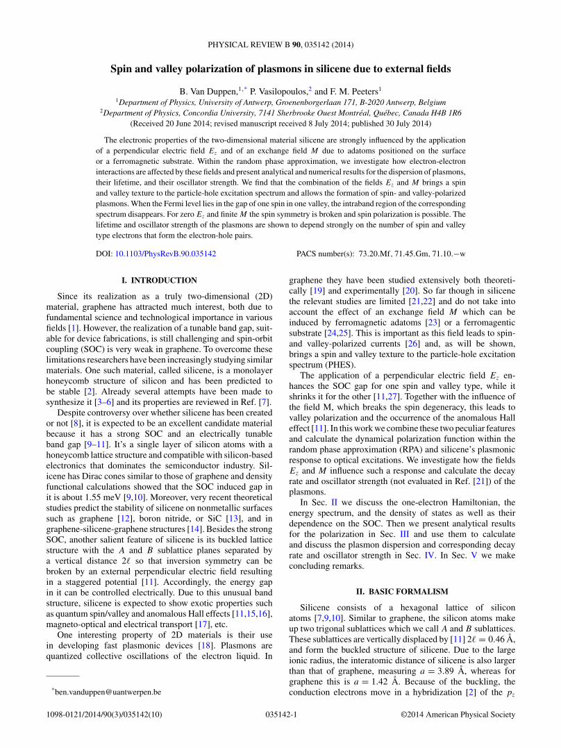
In Fig. 1 we show the energy spectrum for λSO = 3.9 meVand several combinations of Ez and M values near both valleys.In the Hamiltonian (1) three types of SOC are included. One isrepresented by the parameter λSO and introduces a gap in thespectrum as shown in Fig. 1(a). It is diagonal in the spin basis,so both spin components are treated equally. The terms λR1
and λR2 do mix up the spin states. However, as shown below,the effect of these terms is very small and the spin remains anapproximate good quantum number.
The term λR1(Ez) describes the Rashba SOC due to thefield Ez. Note, however, that for a wide range of Ez values
FIG. 1. (Color online) Energy spectrum of silicene versus wavevector k in the K+ (left column) and the K− valleys (right column)for different values of the electric Ez and exchange M fields, asspecified, and λSO = 3.9 meV. The blue dashed curves pertain tosz = +1 electrons and the red dash-dotted curve to sz = −1 electronswhen the terms λR2 are neglected. The dotted lines show the Fermilevel μ0 = 13 meV. This μ0 value will be used in the entire paper.
this term can be safely neglected since at fields of the orderof the critical field Ec = λSO/�, its value is approximatelyλR1 ≈ 10−3λSO [9,11,29].
A unitary transformation of Eq. (2) allows more insight intothe importance of λR2. With the combinations
ψ1 = [�vF ψB↑ + iaλR2ψA↓]/�v′F , (3)
ψ2 = [�vF ψA↓ + iaλR2ψB↑]/�v′F , (4)
where �v′F = �vF (1 + ξ 2)1/2 and ξ = aλR2/�vF ≈ 0.5 ×
10−3, the new basis �sz= {ψA↑,ψ1,ψ2,ψB↓}T transforms
Eq. (2) into the form
H ′+ =
⎡⎢⎣
E(1,1) �v′F k− 0 0
�v′F k+ E(1,−1) − 2M ′ξ 2 −2iM ′c 00 2iM ′c E(−1,1) + 2M ′ξ 2
�v′F k−
0 0 �v′F k+ E(−1,−1)
⎤⎥⎦ , (5)
where M ′ = �Ez + M and c = ξ/(1 + ξ 2)1/2.
035142-2
SPIN AND VALLEY POLARIZATION OF PLASMONS IN . . . PHYSICAL REVIEW B 90, 035142 (2014)
The effect of λR2 is thus threefold. To first order in ξ
it induces a change in the Fermi velocity, vF → v′F , and it
couples the spin components by virtue of a finite electric Ez
or exchange M field. Additionally, it affects the gap to secondorder in ξ by a diagonal term that is linear in Ez and M .However, these effects are very small due to the smallness ofξ . We shall therefore neglect λR2.
B. Effective Hamiltonian
The approximations referred to above decouple the twospin states. Because the valleys are independent, we candescribe electrons in silicene as particles that have a spin- andvalley-dependent gap. In the basis �ηsz
= {ψA,ηsz,ψB,ηsz
}T theHamiltonian becomes
Hsz
η =[ηsz
+ szM �vF ηkη−
�vF ηkη+ −ηsz
+ szM
], (6)
where sz = ±1 is the spin quantum number, η denotes thevalley and k
η± equals k± for η = +1 and k∗
± for η = −1.The gap is independent of M and given by
2∣∣ηsz
∣∣ = 2|ηszλSO − �Ez|. (7)
Equation (6) corresponds to a 2D Dirac Hamiltonian ofparticles with mass ηsz
. Note that in graphene because of thelow buckling, both the SOC and the effect of an electric fieldon the gap are negligible [29]. The energy spectrum obtainedfrom Eq. (6) reads
Esz
η = szM + λ[�
2v2F k2 + 2
ηsz
]1/2, (8)
where λ = 1(−1) denotes the electron (hole) states. We showit for all spin and valley components in Fig. 1 for differentvalues of �Ez and M . In Fig. 1(b) �Ez attains its critical valueEc = λSO/�, for which the sz = +1 spin component has alinear massless dispersion, while the sz = −1 one has a largegap near the K+ point. In Fig. 1(c) the field M is finite; itdisplaces both spin components in opposite directions andresults in a spectrum that is different for each spin and valleytype of electron. In Fig. 1(d) only the M field is present andleads to spin polarization but the valleys remain equivalent.
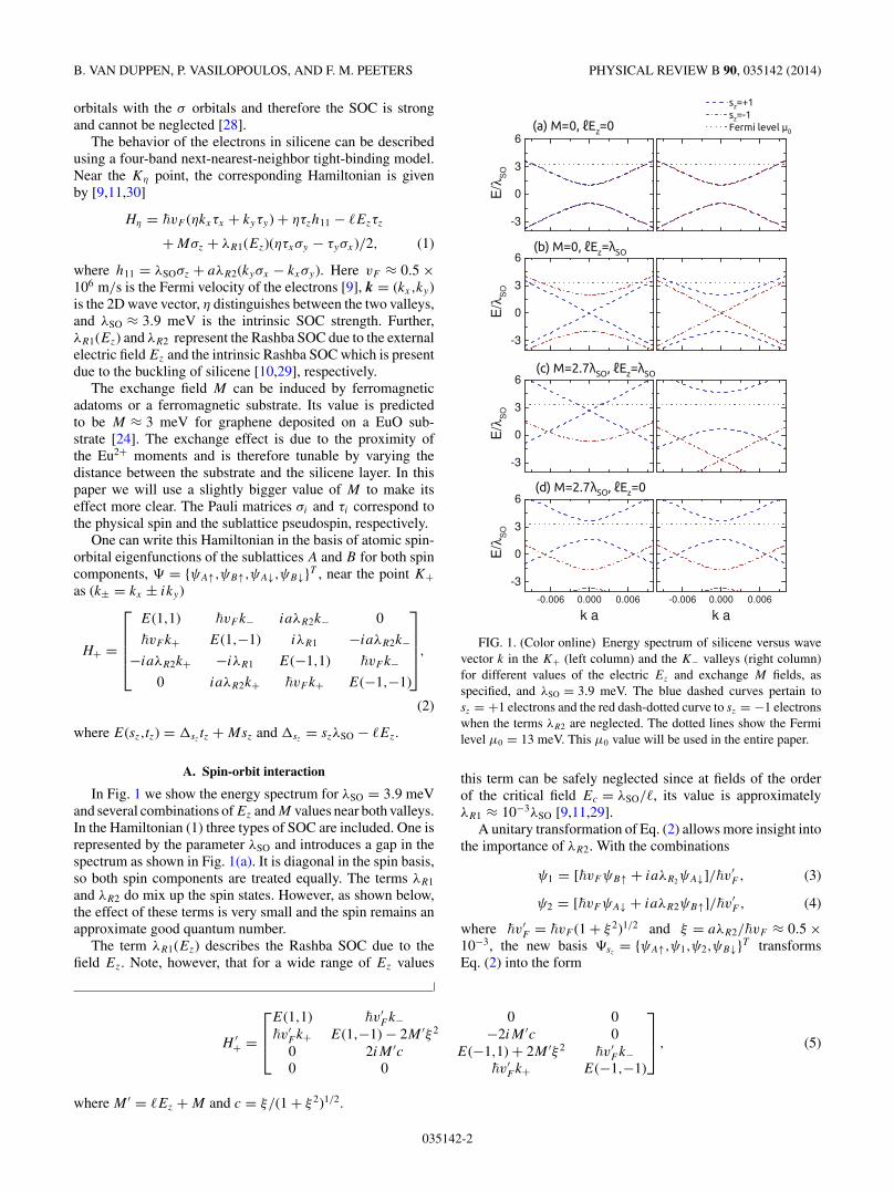
This energy spectrum gives rise to a density of states D(E)(DOS) with a structure that depends sensitively on the valuesof the electric Ez and exchange M fields. With E = E − szM
the full expression for D(E) is [30]
D(E) =∑η=±1
∑sz=±1
|E|2π�2v2
F
�(|E| − ∣∣ηsz
∣∣). (9)
We show D(E) in Fig. 2 for various values of �Ez and M .Notice that the DOS depends heavily on the spin and valleyindex of the electrons. In Figs. 2(c) and 2(d), for example,the total DOS is constant near zero energy, but it nonethelessconsists of different portions of spin-up and spin-down statesfor each energy.
FIG. 2. (Color online) DOS in silicene for different values, spec-ified, of the electric Ez and exchange M fields. The solid black curveis the total DOS. The other curves correspond to different valleys andspins as shown at the top of the figure. The DOS is expressed as adimensionless quantity defined by D′(E) = (2π�
2v2F /λSO)D(E).
III. POLARIZATION IN SILICENE
To assess electron-electron interactions in the RPA, we firstneed to determine the polarization [31–35]:
0(q,ω) =∑η=±1
∫dν d2k
(2π )3Tr
[G0
η(k,ν)G0η(k + q,ν + ω)
],
(10)where the summation over η corresponds to different valleysand G0
η(k,ν) is the Green’s function of the noninteracting par-ticle near the Kη valley. For a finite-mass Dirac Hamiltonian,such as the one shown in Eq. (6), the Green’s function is givenby [31,32]
G0ηsz
(k,ω) = (�ω + μ0 − Hsz
η
)−1
= �ω + μ0 − 2szM + Hszη
(�ω + μ0 − szM)2 − (�vF k)2 − 2ηsz
, (11)
where we have omitted the identity matrices for the sake ofbrevity and k is the magnitude of k. Notice that the dependenceof the Green’s function on the spin quantum number sz istwofold: on the one hand it changes the Fermi level μ0 toμsz
= μ0 − szM and on the other it influences the gap givenby ηsz
defined in Eq. (7).We consider only the reduced Hamiltonian (6). For the
complete 4 × 4 Hamiltonian, we obtain both Green’s functionsalong the diagonal, so
G0η(k,ν) =
[G0
η,+1(k,ν) 0
0 G0η,−1(k,ν)
]. (12)
We can readily calculate the trace in Eq. (10) and write thetotal polarization as
0(q,ω) =∑η=±1
∑sz=±1
0ηsz
(q,ω), (13)
035142-3
B. VAN DUPPEN, P. VASILOPOULOS, AND F. M. PEETERS PHYSICAL REVIEW B 90, 035142 (2014)
with the spin- and valley-dependent polarization, obtained inthe manner of Ref. [35], given by
0ηsz
(q,ω) = 1
2
∫d2k
(2π )2
∑λλ′=±1
f λλ′ηsz
(k,q)
× nsz
F
(λE
ηsz
k
) − nsz
F
(λ′Eηsz
k+q
)�ω + λ′Eηsz
k − λEηsz
k+q + iδ; (14)
here δ is an infinitesimal positive quantity, nsz
F is the Fermi-Dirac distribution with a spin-dependent Fermi level μsz
,E
ηszq = [�2v2
F q2 + 2ηsz
]1/2, and f λλ′ηsz
is the structure factor
f λλ′ηsz
(k,q) =[
1 + λλ′ k(k + q) + 2ηsz
Eηszq E
ηsz
k+q
]. (15)
Equation (15) expresses the pseudospinorial character ofelectrons in silicene and will prevent two oppositely movingones from interacting if the gap ηsz
is zero. This factor istypical for graphenelike 2D systems such as silicene.
Since transitions between different spin and valley statescan be neglected, as previously motivated, the resultingpolarization is a sum of independent systems. These systemsare analogous to gapped graphene [35] but in each of them onecan change the size of the gap separately by varying the fieldEz and the Fermi level can be tuned by changing the field M .The spin and valley components are influenced by these fieldsin different ways.
The contributions to the polarization from Eq. (14) can bewritten as a sum of three parts [36,37]
0ηsz
= − −ηsz,∞ + +
ηsz,μsz+ −
ηsz,μsz, (16)
where ±ηsz,μ
= ±ηsz,μ
(q,ω) stands for interband (−) or intra-band (+) contributions with Fermi level μ. The last two termscontribute only for μsz
> ηsz. Note that because the Fermi
level μ0 is fixed, while the spectrum is displaced or deformeddue to the field Ez or M , it is possible that this inequality isreversed for one valley spin state while it still holds for theothers. In such a case only the vacuum polarization −
ηsz,∞contributes to the polarization of the respective state. Differentpossible situations are depicted in Fig. 1 in which the Fermilevel is shown as a black dotted line. In Figs. 1(a) and 1(b) theFermi level lies in the conduction band of all spin and valleytype electrons such that intraband transitions are possible. InFig. 1(c), however, this is not the case for spin-up electrons nearthe K− valley. The combination of the M and Ez fields is suchthat the Fermi level lies in the band gap of this type of electronand therefore intraband transitions are excluded in this case.In Fig. 1(d) the two valleys are equivalent as discussed earlier,but the Fermi level lies in the gap of the spin-up electrons andexcludes intraband transitions for them.
Analytical solutions have been found for both the vacuumpolarization [31,35,38] and the polarization in graphene with apartly filled conduction band [35]. The polarization for μsz
>
ηszcan be written as
0ηsz,μ0
(q,ω)
D0(μ0)= −
[μ′
sz− q ′2
8 aq ′Fηsz
(q,ω)
], (17)
where a2q ′ = |q ′2 − ω′2|, q ′ = �vF q/μ0, ω′ = �ω/μ0, and
μ′sz
= μsz/μ0. Further, D0(E) = |E|/[2π�
2v2F ] is the density
of states for one spin component near one Dirac point ifE > ηsz
and Fηsza dimensionless function that acquires
different values in different parts of the (q,ω) plane as shownin the Appendix.
On the other hand, the vacuum polarization reads
0sz,vac(q,ω)
D0(μ0)= − q ′2
aq ′
[′
ηsz
2 aq ′+ Fηsz,vac(q,ω)
], (18)
where a2q ′ = |q ′2 − ω2| and ′
ηsz= ηsz
/μ0. Fηsz,vac is adimensionless function defined in the Appendix. Combiningthese results, the total polarization is given by
0ηsz
= θ(μsz
− ηsz
) 0
ηsz,μ0+ θ
(ηsz
− μsz
) 0
ηsz,vac.
(19)
The complete expression of the dynamical polarization isgiven in the Appendix. The static one can be written as
0ηsz,μ0
(q,0)
D0(μ0)= −
[μ′
sz− 1
4θ (q − 2qF,sz
)
×(
2μ′szbq ′
q ′ − cq ′
q ′ arctanbq ′
2μ′sz
)], (20)
0ηsz,vac(q,0)
D0(μ0)= −1
2
[′
ηsz+ c2
q ′
2q ′ arcsinq ′
cq ′
],
where bq ′ = [q ′2 − 4q ′2F,sz
]1/2 and cq ′ = [q ′2 − 4′2sz
]1/2; weused the definition of the Fermi wave vector qF,ηsz
=�vF [μ2
sz− 2
ηsz]1/2. For M = 0 Eq. (20) coincides with the
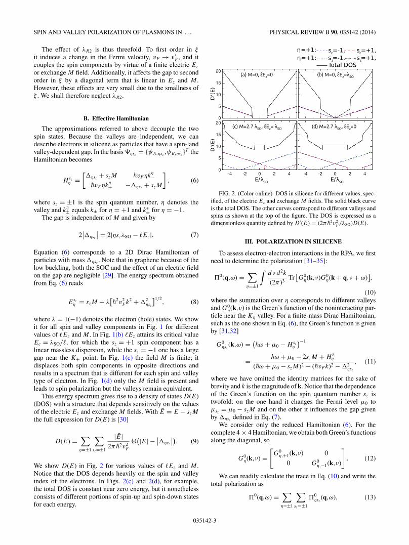
result of Ref. [21] and for M = Ez = 0 and λSO = withthat of Ref. [35]. In Fig. 3 we show the static polarizationfor various values of the fields Ez and M . This figure showsthat as long as all spin and valley type electrons contribute,for low q, the static polarization equals the DOS at the Fermilevel, D(μ0), which is the case for the blue dashed and red
FIG. 3. (Color online) Static polarization versus wave vector q ′
for different values of the fields Ez and M . The Fermi level is μ0 =13 meV and the SOC λSO = 0.3μ0. The blue dashed curve is for Ez =M = 0, and the red dotted one for the critical field Ez = Ec = λSO/�
and M = 0. Further, the green dash-dotted curve is for M = 2.7λSO
and �Ez = λSO, and the purple dash-dot-dotted one for �Ez = 0 andM = 2.7λSO.
035142-4
SPIN AND VALLEY POLARIZATION OF PLASMONS IN . . . PHYSICAL REVIEW B 90, 035142 (2014)
dotted curves. However, when this is not the case, as for theother two curves, the polarization decreases because, in thiscase, for some spin and valley type electrons only interbandcontributions are allowed.
Furthermore, one can approximate the polarization at smallenergies and momenta, �vF k �ω μ, as [35]
0ηsz
(q,ω)
D0(μ0)= q ′2μ′
sz
2ω′2
(1 − ′2
ηsz
μ′2sz
)θ(′
ηsz− μ′
sz
), (21)
which is valid for all values of μszand ηsz
.
A. Particle-hole excitation spectrum (PHES)
The PHES is the region in the (q,ω) plane where it ispossible for a photon with energy �ω and momentum �q toexcite an electron-hole pair. This ability for pair creation isembodied in the polarization, in the regions where it has anonzero imaginary part. The PHES can be divided into twodisjunct regions where inter- and intraband electron-hole pairformation is possible. These regions are located above andbelow the ω′ = q ′ line, respectively. Because the fields Ez andM change the structure of the bands and the position of theFermi level, the PHES is also subject to changes in their values.Since the valley and spin of the electrons determine how thefields affect their dispersion and Fermi level, the PHES can bedifferent for electrons with different spin or valley index.
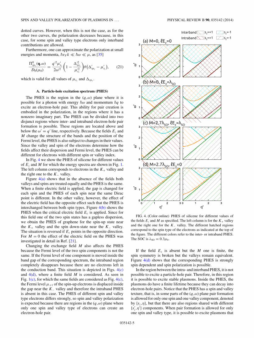
In Fig. 4 we show the PHES of silicene for different valuesof Ez and M for which the energy spectra are shown in Fig. 1.The left column corresponds to electrons in the K+ valley andthe right one to the K− valley.
Figure 4(a) shows that in the absence of the fields bothvalleys and spins are treated equally and the PHES is the same.When a finite electric field is applied, the gap is changed foreach spin and the PHES of each spin near the same Diracpoint is different. In the other valley, however, the effect ofthe electric field has the opposite effect such that the PHES isinterchanged between both spin types. Figure 4(b) shows thePHES when the critical electric field Ec is applied. Since forthis field one of the two spin states has a gapless dispersion,we obtain the PHES of graphene for the spin-up state nearthe K+ valley and the spin down-state near the K− valley.The situation is reversed if Ec points in the opposite direction.For M = 0 the effect of the electric field on the PHES wasinvestigated in detail in Ref. [21].
Changing the exchange field M also affects the PHESbecause the Fermi level of the two spin components is not thesame. If the Fermi level of one component is moved inside theband gap of the corresponding spectrum, the intraband regioncompletely disappears because there are no electrons left inthe conduction band. This situation is depicted in Figs. 4(c)and 4(d), where a finite field M is considered. As seen inFig. 1(c), for which the same fields are considered as Fig. 4(c),the Fermi level μ+1 of the spin-up electrons is displaced insidethe gap near the K− valley and therefore the intraband PHESis absent in this case. The PHES of different spin and valleytype electrons differs strongly, so spin and valley polarizationis expected because there are regions in the (q,ω) plane whereonly one spin and valley type of electrons can create anelectron-hole pair.
FIG. 4. (Color online) PHES of silicene for different values ofthe fields Ez and M as specified. The left column is for the K+ valleyand the right one for the K− valley. The different hatched regionscorrespond to the spin type of the electrons as indicated at the top ofthe figure. The different colors refer to the inter- or intraband PHES.The SOC is λSO = 0.3μ0.
If the field Ez is absent but the M one is finite, thespin symmetry is broken but the valleys remain equivalent.Figure 4(d) shows that the corresponding PHES is stronglyspin dependent and spin polarization is possible.
In the region between the intra- and interband PHES, it is notpossible to excite a particle-hole pair. Therefore, in this regionit is possible to excite stable plasmons. Inside the PHES, theplasmons do have a finite lifetime because they can decay intoelectron-hole pairs. Notice that the PHES has a spin and valleytexture, that is, in some parts of the (q,ω) plane pair formationis allowed for only one spin and one valley component, denotedby {sz,η}, but that there are also regions shared with different{s ′
z,η′} components. When pair formation is allowed for only
one spin and valley type, it is possible to excite plasmons that
035142-5
B. VAN DUPPEN, P. VASILOPOULOS, AND F. M. PEETERS PHYSICAL REVIEW B 90, 035142 (2014)
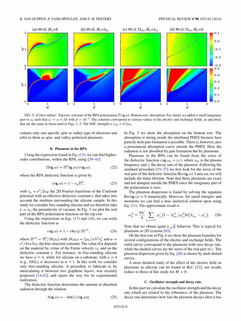
FIG. 5. (Color online) Top row: real part of the RPA polarization ′(q,ω). Bottom row: absorption. For clarity we added a small imaginarypart to ω, such that ω → ω + Iβ with β = 10−4. The columns correspond to various values of the electric and exchange fields, as specified,that are the same as those used in Figs. 1–3. The SOC strength is λSO = 0.3μ0.
contain only one specific spin or valley type of electrons andrefer to them as spin- and valley-polarized plasmons.
B. Plasmons in the RPA
Using the expression found in Eq. (13), we can find higher-order contributions, within the RPA, using [39–41]
(q,ω) = 0(q,ω)/ε(q,ω), (22)
where the RPA dielectric function is given by
ε(q,ω) = 1 − vq 0, (23)
with vq = e2/2κq the 2D Fourier transform of the Coulombpotential with an effective dielectric constant κ that takes intoaccount the medium surrounding the silicene sample. In thisstudy we consider free-standing silicene and we therefore takeκ = ε0, the permittivity of vacuum. In Fig. 5 we plot the realpart of the RPA polarization function on the top row.
Using the expressions in Eqs. (17) and (18), we can writethe dielectric function as
ε(q,ω) = 1 − (4α/q ′) ′,0, (24)
where ′,0 = 0/D(μ0) with D(μ0) = 2μ0/π�2v2
F and α =e2/4πκ�vF the fine-structure constant. The value of α dependson the material by virtue of the Fermi velocity vF and on thedielectric constant κ . For instance, in free-standing silicenewe have α ≈ 4, while for silicene on a substrate, with κ = 4(e.g., SiO2), α decreases to α ≈ 1. In this work we consideronly free-standing silicene. A procedure to fabricate it, byintercalating it between two graphene layers, was recentlyproposed [14,42], and opens the way for its experimentalrealization.
The dielectric function determines the amount of absorbedradiation through the relation
A(q,ω) = −Im[1/ε(q,ω)]. (25)
In Fig. 5 we show the absorption on the bottom row. Theabsorption is strong inside the interband PHES because hereparticle-hole pair formation is possible. There is, however, alsoa pronounced absorption curve outside the PHES. Here theradiation is not absorbed by pair formation but by plasmons.
Plasmons in the RPA can be found from the zeros ofthe dielectric function ε(q,ωp + iγ ), where ωp is the plasmafrequency and γ the decay rate of the plasmon. Following thestandard procedure [35–37] we first look for the zeros of thereal part of the dielectric function Reε(q,ω). Later on, we willinclude the finite lifetime. Note that these plasmons are exactand not damped outside the PHES since the imaginary part ofthe polarization is zero.
The plasmon dispersion is found by solving the equationReε(q,ω) = 0 numerically. However, for small energies andmomenta we can find a near analytical solution upon usingEq. (21). The approximate result is
ω′2p ≈ αq ′
8
∑η,sz=±1
μ′sz
(1 − ′2
ηsz/μ′2
sz
)θ(′
ηsz− μ′
sz
). (26)
Note that we obtain again a√
q behavior. This is typical forplasmons in 2D systems [43].
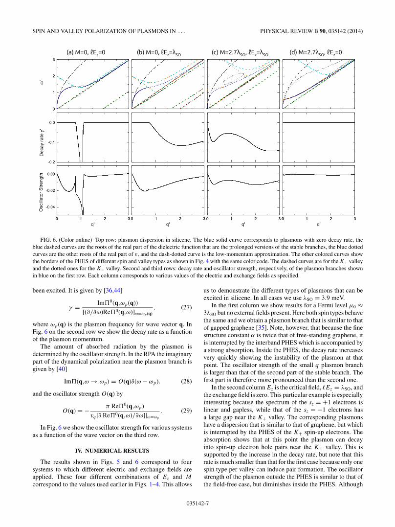
On the first row of Fig. 6 we show the plasmon branches forseveral configurations of the electric and exchange fields. Thesolid curves correspond to the plasmons with zero decay rate,while the dashed curves are the zeros of the real part of ε. Theplasmon dispersion given by Eq. (26) is shown by dash-dottedcurves.
A more detailed study of the effect of the electric field onplasmons in silicene can be found in Ref. [21]; our resultsreduce to those of this study for M = 0.
C. Oscillator strength and decay rate
In this part we calculate the oscillator strength and the decayrate which are related to the robustness of the plasmon. Thedecay rate determines how fast the plasmon decays after it has
035142-6
SPIN AND VALLEY POLARIZATION OF PLASMONS IN . . . PHYSICAL REVIEW B 90, 035142 (2014)
FIG. 6. (Color online) Top row: plasmon dispersion in silicene. The blue solid curve corresponds to plasmons with zero decay rate, theblue dashed curves are the roots of the real part of the dielectric function that are the prolonged versions of the stable branches, the blue dottedcurves are the other roots of the real part of ε, and the dash-dotted curve is the low-momentum approximation. The other colored curves showthe borders of the PHES of different spin and valley types as shown in Fig. 4 with the same color code. The dashed curves are for the K+ valleyand the dotted ones for the K− valley. Second and third rows: decay rate and oscillator strength, respectively, of the plasmon branches shownin blue on the first row. Each column corresponds to various values of the electric and exchange fields as specified.
been excited. It is given by [36,44]
γ = Im 0(q,ωp(q))
[(∂/∂ω)Re 0(q,ω)]ω=ωp(q), (27)
where ωp(q) is the plasmon frequency for wave vector q. InFig. 6 on the second row we show the decay rate as a functionof the plasmon momentum.
The amount of absorbed radiation by the plasmon isdetermined by the oscillator strength. In the RPA the imaginarypart of the dynamical polarization near the plasmon branch isgiven by [40]
Im (q,ω → ωp) = O(q)δ(ω − ωp). (28)
and the oscillator strength O(q) by
O(q) = − π Re 0(q,ωp)
vq |∂ Re 0(q,ω)/∂ω]|ω=ωp
. (29)
In Fig. 6 we show the oscillator strength for various systemsas a function of the wave vector on the third row.
IV. NUMERICAL RESULTS
The results shown in Figs. 5 and 6 correspond to foursystems to which different electric and exchange fields areapplied. These four different combinations of Ez and M
correspond to the values used earlier in Figs. 1–4. This allows
us to demonstrate the different types of plasmons that can beexcited in silicene. In all cases we use λSO = 3.9 meV.
In the first column we show results for a Fermi level μ0 ≈3λSO but no external fields present. Here both spin types behavethe same and we obtain a plasmon branch that is similar to thatof gapped graphene [35]. Note, however, that because the finestructure constant α is twice that of free-standing graphene, itis interrupted by the interband PHES which is accompanied bya strong absorption. Inside the PHES, the decay rate increasesvery quickly showing the instability of the plasmon at thatpoint. The oscillator strength of the small q plasmon branchis larger than that of the second part of the stable branch. Thefirst part is therefore more pronounced than the second one.
In the second column Ez is the critical field, �Ez = λSO, andthe exchange field is zero. This particular example is especiallyinteresting because the spectrum of the sz = +1 electrons islinear and gapless, while that of the sz = −1 electrons hasa large gap near the K+ valley. The corresponding plasmonshave a dispersion that is similar to that of graphene, but whichis interrupted by the PHES of the K+ spin-up electrons. Theabsorption shows that at this point the plasmon can decayinto spin-up electron hole pairs near the K+ valley. This issupported by the increase in the decay rate, but note that thisrate is much smaller than that for the first case because only onespin type per valley can induce pair formation. The oscillatorstrength of the plasmon outside the PHES is similar to that ofthe field-free case, but diminishes inside the PHES. Although
035142-7
B. VAN DUPPEN, P. VASILOPOULOS, AND F. M. PEETERS PHYSICAL REVIEW B 90, 035142 (2014)
the PHES and the plasmons in the two valleys depend on thespin type, they are compensated in the other valley. Therefore,in this case the plasmons are not spin polarized.
In the third column the electric and exchange fields arefinite. Because of the combined effect of both fields, the PHESacquires a spin and valley texture. For very small q the plasmonbranch is stable but it quickly encounters the border of the K+spin-up PHES where the decay rate increases. The branchcontinues under the border of the K− spin-up PHES but thestrong absorption signals its presence. The crossing of theborder of the K− spin-down PHES results in a shorteningof the lifetime because the plasmons can decay into twodifferent types of electrons, the spin-up type in the K+ valleyand the spin down one in the K− valley. Thus, in this case,we obtain spin- and valley-polarized plasmons. Notice anadditional feature, the oval dotted curve; this is the remnant ofthe plasmon branch of spin-down electrons.
The fourth column applies to the case where the electricfield is absent but a very large exchange field is applied, M ≈2.7λSO. In this situation the dispersions of both spin typesare shifted with respect to each other in such a way that theFermi level lies in the gap of the spin-up electrons while it issituated in the conduction band of the spin-down electrons. Forspin-up electrons the intraband PHES therefore vanishes andthe interband PHES is shifted to lower energies. Here there isan undamped plasmon branch that follows the border of theinterband PHES of the spin-up electrons. Despite its stability,the oscillator strength and absorption show that it is not verypronounced. There exists, however, also a strongly dampedbranch that lies inside the spin-up interband PHES, shownby the dotted curve, which is the prolonged version of theundamped plasmon and shows the same
√q dependence of the
stable plasmon for low q. This branch indicates a spin-downplasmon but one which can decay very quickly into spin-upelectron-hole pairs leading to a strong absorption in this regionas shown in Fig. 5(d). This plasmon lies outside the PHES andis therefore neither spin nor valley polarized. However, theplasmonlike branch inside the spin-up PHES does resemble aspin-polarized system but with a very short lifetime.
V. CONCLUDING REMARKS AND OUTLOOK
We investigated how electric (Ez) and exchange (M) fieldscan be used to tune the plasmonic response of the electrongas in silicene. These fields affect the PHES of electrons withopposite spin and valley indices in different ways giving thePHES a spin and valley texture and thus leading to spin- andvalley-polarized plasmons. Their lifetime is, however, finitebecause they can easily decay into electron-hole pairs withdifferent spin or valley indices. Further, the field M affectsstrongly the oscillator strength. The undamped plasmon thatremains has a negligible strength and is therefore not expectedto show up in experiments. If the Fermi level lies in the gap ofa spin in one valley, the intraband region of the correspondingPHES disappears. For zero Ez and finite M the spin symmetryis broken and spin polarization is possible.
We found a low-momentum plasmon dispersion that has thetypical 2D
√q behavior. At higher momentum, the plasmon
dispersion differs from this√
q dependence. However, a strongfield M can induce plasmons with finite lifetime of one spin
type for which the dispersion follows closely the approximateplasmon branch.
The results reported in this work pertain to free-standingsilicene since we used the permittivity ε0 of the vacuum.For silicene on a substrate the permittivity will be differentand the results will be modified quantitatively. The plasmonbranches will be curved downward and the PHES can beavoided yielding plasmons with larger oscillator strength.
We evaluated the plasmon dispersion within the frameworkof the RPA which is valid for high electron densities. For lowerdensities further work is necessary to obtain more accurateresults for silicene’s plasmonic properties.
The predicted spin and valley polarization of plasmons isa consequence of a mechanism similar to that responsible fordirectional filtering of plasmons in a 2D electron gas [45]. Inthis case the anisotropy of the electron dispersion renders thePHES anisotropic and damps the plasmons in one directionmore than in the other.
Recently a lot of experimental progress has been made inthe detection of plasmons in 2D materials [46]. To overcomethe mismatch of energy and momentum with light in freespace, one uses a periodic diffractive grid, cuts the sheetinto ribbons or other shapes, and uses an AFM tip to excitethe electron liquid or uses a resonant metal antenna [47].The appropriate experimental probe though will stronglydepend on the setup used to stabilize the silicene crystal. Webelieve that at the current pace of experimental progress, inthe creation of silicene and the probing of plasmons in 2Dmaterials, the results presented in this paper will soon be testedexperimentally.
ACKNOWLEDGMENTS
This work was supported by the European ScienceFoundation (ESF) under the EUROCORES Program Euro-GRAPHENE within the project CONGRAN, the FlemishScience Foundation (FWO-Vl) by an aspirant grant to B.V.D.,the Methusalem Foundation of the Flemish Government, andby the Canadian NSERC Grant No. OGP0121756.
APPENDIX: ANALYTICAL FORMULAE
The results for the polarization shown in Eqs. (17) and (18)each depend on a dimensionless function that determines thevariation of the polarization in the (q,ω) plane. For the vacuumpolarization this function is given in terms of the dimensionlessvariables q ′, ω′, and μ′
szdefined earlier. In the following,
we will suppress the prime notation for simplicity and seta2
q = ω2 − q2. Then [35]
Fηsz,vac = 42ηsz
+ a2q
8a2q
[θ (q + ω) arccos
42ηsz
+ a2q
42ηsz
− a2q
+ θ (ω − q) ln
(2sz
+ aq
)2∣∣42ηsz
− a2q
∣∣]
+ iπ
8
(a2
q − 42ηsz
a2q
)θ(a2
q − 42ηsz
). (A1)
035142-8
SPIN AND VALLEY POLARIZATION OF PLASMONS IN . . . PHYSICAL REVIEW B 90, 035142 (2014)
With y± = (2μsz± ω)/q, xηsz
= [1 + 42ηsz
/(q2 − ω2)]1/2,and x2
ηsz= 2 − x2
ηsz, the total polarization for μsz
> ηsz
is [35]
Fηsz(q,ω) =
⎧⎪⎪⎪⎪⎪⎪⎪⎪⎪⎪⎪⎪⎪⎪⎪⎨⎪⎪⎪⎪⎪⎪⎪⎪⎪⎪⎪⎪⎪⎪⎪⎩
iG>(y−) − iG>(y+) : 1A,
G<(y−) − iG>(y+) : 2A,
G<(y+) + G<(y−) : 3A,
G<(y−) − G<(y+) : 4A,
G>(y+) − G>(y−) : 1B,
G>(y+) + iG<(y−) : 2B,
G>(y+) − G>(−y−) − iπx2ηsz
: 3B,
G>(−y−) + G>(y+) − iπx2ηsz
: 4B,
G0(y+) − G0(y−) : 5B.
In these expressions
G<(x) = x[x2
ηsz− x2
]1/2 − x2ηsz
arccos(x/xηsz), (A2)
G>(x) = x[x2 − x2
ηsz
]1/2 − x2ηsz
arcosh(x/xηsz), (A3)
G0(x) = x[x2 − x2
ηsz
]1/2 − x2ηsz
arsinh(x/ixηsz). (A4)
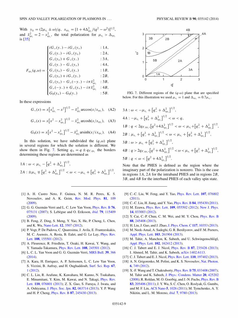
In this solution, we have subdivided the (q,ω) planein several regions for which the solution is different. Weshow them in Fig. 7. Setting q± = q ± qF,ηsz
the bordersdetermining these regions are determined as
1A : ω < μsz− [
q2− + 2
ηsz
]1/2,
2A : ±μsz∓ [
q2− + 2
ηsz
]1/2< ω < −μsz
+ [q2
+ + 2ηsz
]1/2,
FIG. 7. Different regions of the (q-ω) plane that are specifiedbelow. For this illustration we used μsz = 1 and ηsz = 0.7μsz .
3A : ω < −μsz+ [
q2− + 2
ηsz
]1/2,
4A : −μsz+ [
q2+ + 2
ηsz
]1/2< ω < q,
1B : q < 2qF,ηsz,[q2+42
ηsz
]1/2< ω < μsz
+[q2
− + 2ηsz
]1/2,
2B : μsz+ [
q2− + 2
ηsz
]1/2< ω < μsz
+ [q2
+ + 2ηsz
]1/2,
3B : ω > μsz+ [
q2+ + 2
ηsz
]1/2,
4B : q > 2qF,ηsz,[q2 + 42
ηsz
]1/2< ω < μsz
+ [q2
− + 2ηsz
]1/2,
5B : q < ω <[q2 + 42
ηsz
]1/2.
Note that the PHES is defined as the region where theimaginary part of the polarization is nonzero. This is the casein regions 1A, 2A for the intraband PHES and in regions 2B,3B, and 4B for the interband PHES of each valley spin state.
[1] A. H. Castro Neto, F. Guinea, N. M. R. Peres, K. S.Novoselov, and A. K. Geim, Rev. Mod. Phys. 81, 109(2009).
[2] G. G. Guzman-Verri and L. C. Lew Yan Voon, Phys. Rev. B 76,075131 (2007); S. Lebegue and O. Eriksson, ibid. 79, 115409(2009).
[3] B. Feng, Z. Ding, S. Meng, Y. Yao, X. He, P. Cheng, L. Chen,and K. Wu, Nano Lett. 12, 3507 (2012).
[4] P. Vogt, P. De Padova, C. Quaresima, J. Avila, E. Frantzeskakis,M. C. Asensio, A. Resta, B. Ealet, and G. Le Lay, Phys. Rev.Lett. 108, 155501 (2012).
[5] A. Fleurence, R. Friedlein, T. Ozaki, H. Kawai, Y. Wang, andY. Yamada-Takamura, Phys. Rev. Lett. 108, 245501 (2012).
[6] L. C. L. Yan Voon and G. G. Guzman-Verri, MRS Bull. 39, 366(2014).
[7] A. Kara, H. Enriquez, A. P. Seitsonen, L. C. Lew Yan Voon,S. Vizzini, B. Aufray, and H. Oughaddoub, Surf. Sci. Rep. 67,1 (2012).
[8] C. L. Lin, R. Arafune, K. Kawahara, M. Kanno, N. Tsukahara,E. Minamitani, Y. Kim, M. Kawai, and N. Takagi, Phys. Rev.Lett. 110, 076801 (2013); Z. X. Guo, S. Furuya, J. Iwata, andA. Oshiyama, J. Phys. Soc. Jpn. 82, 063714 (2013); Y. P. Wangand H. P. Cheng, Phys. Rev. B 87, 245430 (2013).
[9] C.-C. Liu, W. Feng, and Y. Yao, Phys. Rev. Lett. 107, 076802(2011).
[10] C.-C. Liu, H. Jiang, and Y. Yao, Phys. Rev. B 84, 195430 (2011).[11] M. Ezawa, Phys. Rev. Lett. 109, 055502 (2012); ,New J. Phys.
14, 033003 (2012).[12] Y. Cai, C.-P. Chuu, C. M. Wei, and M. Y. Chou, Phys. Rev. B
88, 245408 (2013).[13] H. Liu, J. Gao, and J. Zhao, J. Phys. Chem. C 117, 10353 (2013).[14] M. Neek-Amal, A. Sadeghi, G. R. Berdiyorov, and F. M. Peeters,
Appl. Phys. Lett. 103, 261904 (2013).[15] M. Tahir, A. Manchon, K. Sabeeh, and U. Schwingenschlogl,
Appl. Phys. Lett. 102, 162412 (2013).[16] C. J. Tabert and E. J. Nicol, Phys. Rev. B 87, 235426 (2013);
I. Ahmed, M. Tahir, and K. Sabeeh, arXiv:1402.6113.[17] C. J. Tabert and E. J. Nicol, Phys. Rev. Lett. 110, 197402 (2013).[18] A. N. Grigorenko, M. Polini, and K. S. Novoselov, Nat. Photon.
6, 749 (2012).[19] X.-F. Wang and T. Chakraborty, Phys. Rev. B 75, 033408 (2007);
M. Tahir and K. Sabeeh, J. Phys.: Condens. Matter 20, 425202(2008); R. Roldan, M. O. Goerbig, and J.-N. Fuchs, Phys. Rev. B83, 205406 (2011); J. Y. Wu, S. C. Chen, O. Roslyak, G. Gumbs,and M. F. Lin, ACS Nano 5, 1026 (2011); M. Tymchenko, A. Y.Nikitin, and L. M. Moreno, ibid. 7, 9780 (2013).
035142-9
B. VAN DUPPEN, P. VASILOPOULOS, AND F. M. PEETERS PHYSICAL REVIEW B 90, 035142 (2014)
[20] I. Crassee, M. Orlita, M. Potemski, A. L. Walter, M. Ostler,Th. Seyller, I. Gaponenko, J. Chen, and A. B. Kuzmenko,Nano Lett. 12, 2470 (2012); H. G. Yan, Z. Li, X. Li, W. Zhu,P. Avouris, and F. Xia, ibid. 12, 3766 (2012); J. M. Poumirol,W. Yu, X. Chen, C. Berger, W. A. de Heer, M. L. Smith, T. Ohta,W. Pan, M. O. Goerbig, D. Smirnov, and Z. Jiang, Phys. Rev.Lett. 110, 246803 (2013).
[21] C. J. Tabert and E. J. Nicol, Phys. Rev. B 89, 195410(2014).
[22] H. R. Chang, J. Zhou, H. Zhang, and Y. Yao, Phys. Rev. B 89,201411 (2014).
[23] Z. Qiao, S. A. Yang, W. Feng, W.-K. Tse, J. Ding, Y. Yao,J. Wang, and Q. Niu, Phys. Rev. B 82, 161414 (2010).
[24] H. Haugen, D. Huertas-Hernando, and A. Brataas, Phys. Rev. B77, 115406 (2008).
[25] T. Yokoyama, arXiv:1403.1962.[26] T. Yokoyama, Phys. Rev. B 87, 241409 (2013).[27] N. D. Drummond, V. Zolyomi, and V. I. Falko, Phys. Rev. B 85,
075423 (2012).[28] M. Tahir and U. Schwingenschlogl, App. Phys. Lett. 101,
132412 (2012).[29] H. Min, J. E. Hill, N. A. Sinitsyn, B. R. Sahu, L. Kleinman,
and A. H. MacDonald, Phys. Rev. B 74, 165310 (2006).[30] L. Stille, C. J. Tabert, and E. J. Nicol, Phys. Rev. B 86, 195405
(2012).[31] V. N. Kotov, B. Uchoa, and A. H. Castro Neto, Phys. Rev. B 78,
035119 (2008).[32] V. N. Kotov, V. M. Pereira, and B. Uchoa, Phys. Rev. B 78,
075433 (2008).
[33] V. N. Kotov, B. Uchoa, V. M. Pereira, F. Guinea, and A. H.Castro Neto, Rev. Mod. Phys. 84, 1067 (2012).
[34] S. Das Sarma, S. Adam, E. Hwang, and E. Rossi, Rev. Mod.Phys. 83, 407 (2011).
[35] P. K. Pyatkovskiy, J. Phys.: Condens. Matter 21, 025506(2009).
[36] B. Wunsch, T. Stauber, F. Sols, and F. Guinea, New J. Phys. 8,318 (2006).
[37] E. H. Hwang and S. Das Sarma, Phys. Rev. B 75, 205418 (2007).[38] D. T. Son, Phys. Rev. B 75, 235423 (2007).[39] M. O. Goerbig, Rev. Mod. Phys. 83, 1193 (2011).[40] G. F. Giuliani and G. Vignale, Quantum Theory of the Electron
Liquid (Cambridge University Press, Cambridge, UK, 2005).[41] T. Ando, A. B. Fowler, and F. Stern, Rev. Mod. Phys. 54, 437
(1982).[42] G. R. Berdiyorov, M. Neek-Amal, F. M. Peeters, and A. C. T.
van Duin, Phys. Rev. B 89, 024107 (2014).[43] P. M. Krstajic, B. Van Duppen, and F. M. Peeters, Phys. Rev. B
88, 195423 (2013).[44] A. L. Fetter, J. D. Walecka, Quantum Theory of Many-particle
Systems (Courier Dover, New York, 2003).[45] S. M. Badalyan, A. Matos-Abiague, G. Vignale, and J. Fabian,
Phys. Rev. B 79, 205305 (2009).[46] X. Luo, T. Qiu, W. Lu, and Z. Ni, Mater. Sci. Eng., R 74, 351
(2013).[47] P. Alonso-Gonzalez, A. Y. Nikitin, F. Golmar, A. Centeno,
A. Pesquera, S. Velez, J. Chen, G. Navickaite, F. Koppens,A. Zurutuza, F. Casanova, L. E. Hueso, and R. Hillenbrand,Science 344, 1369 (2014).
035142-10


![INVITED PAPER PlasmonsinGraphene: …soljacic/graphene_Proceedings_IEEE.pdf · Polarization of graphene and plasmons under strain have been investigated in [54] and [55]. Plasmons](https://img.pdfslide.net/doc/110x75/5ae4b30d7f8b9ae1578b4a90/invited-paper-plasmonsingraphene-soljacicgrapheneproceedingsieeepdfpolarization.jpg)