Embed Size (px)
Citation preview
SPIN POLARIZED CURRENT PHENOMENA IN MAGNETIC TUNNEL JUNCTIONS
A DISSERTATION
SUBMITTED TO THE DEPARTMENT OF APPLIED PHYSICS
AND THE COMMITTEE ON GRADUATE STUDIES
OF STANFORD UNIVERSITY
IN PARTIAL FULFILLMENT OF THE REQUIREMENTS
FOR THE DEGREE OF
DOCTOR OF PHILOSOPHY
Li Gao
September 2009

© Copyright by Li Gao 2009
All Rights Reserved
ii
I certify that I have read this dissertation and that, in my opinion, it is fully adequate in scope
and quality as a dissertation for the degree of Doctor of Philosophy.
_________________________________________________
(James S. Harris) Principal Advisor
I certify that I have read this dissertation and that, in my opinion, it is fully adequate in scope
and quality as a dissertation for the degree of Doctor of Philosophy.
_________________________________________________
(Stuart S. P. Parkin) co-Principal Advisor
I certify that I have read this dissertation and that, in my opinion, it is fully adequate in scope
and quality as a dissertation for the degree of Doctor of Philosophy.
_________________________________________________
(Walter A. Harrison)
Approved for the University Committee On Graduate Studies.
_________________________________________________
iii

iv
Abstract
Spin polarized current is of significant importance both scientifically and
technologically. Recent advances in film growth and device fabrication in spintronics
make possible an entirely new class of spin-based devices. An indispensable element in
all these devices is the magnetic tunnel junction (MTJ) which has two ferromagnetic
electrodes separated by an insulator barrier of atomic scale. When electrons flow
through a MTJ, they become spin-polarized by the first magnetic electrode. Thereafter,
the interplay between the spin polarized current and the second magnetic layer
manifests itself via two phenomena:
i.) Tunneling magnetoresistance (TMR) effect. The relative alignment of the electrode
moments determines the resistance and its change. This TMR effect is largely
determined by the spin polarized density states of the electrodes, interface states,
tunneling matrix, and so on. However, despite extensive experimental and
theoretical efforts, many aspects of TMR remain poorly understood. In my
research, it is shown that thin CoFe alloy can be made amorphous by sandwiching
the normally crystalline CoFe electrode between two amorphous layers.
Incorporating amorphous CoFe with Al O to form MTJs, both the TMR and the
tunneling spin polarization are significantly enhanced when the alloy is amorphous.
The tunneling anisotropic magnetoresistance effect in both MgO and Al O based
MTJs is also investigated.
2 3
2 3
ii.) Spin transfer torque (STT) effect. The spin polarized current exerts a torque on the
local moments and can thereby induce steady-state precessional excitation modes or
complete switching of a nanomagnet. This effect has mostly been studied, to date,
in metallic structures where the spin-valve magnetoresistance is small so that the
output power is limited. However, the giant TMR effect in MgO based MTJs,
which also have much higher resistance than spin-valves, can give rise to much
higher rf power output. It is also found that the spectrum is very sensitive to small
variations in device structures, even among devices which exhibit similarly high
TMR (~120%) and have similar resistance-area product (~4-10 Ωμm2).
v

vi
Acknowledgements
First of all, I am deeply grateful for Stuart Parkin’s supervision and support of my Ph.D.
work at the IBM Almaden Research Center. What I learned from him is far beyond
knowledge and skills, and I am greatly impressed by his intelligence, passion, and
innovation. I also really appreciate lots of help from him in my personal life. An
excellent physicist, a great man, I luckily worked with in one important phase of my life.
I would like to sincerely thank Coach for admitting me to Harris group, and
introducing me to the exciting field of spintronics. I especially appreciate his generous
support at the beginning of my studies at Stanford. I thank Coach for his kind and
persistent encouragement and help throughout all my Ph.D. years.
Special acknowledgements to Xin Jiang, without him many of my achievements are
impossible. Thanks to other members of Parkin group for various help, I am honored of
working with them: Masamitsu Hayashi, Rai Moriya, See-Hun Yang, Brian Hughes,
Mahesh Samant, Kevin Roche, Luc Thomas, Hyunsoo Yang, Christian Kaiser,
Nagaphani Aetukuri, Justin Brockman, Cheng-Han Yang, Guenole Jan, Andreas Ney,
Ruisheng Liu, Bastiaan Bergman, Roger Wang, Rekha Rajaram, and Joanna Lankester.
I thank Jonathan Sun for many stimulating discussions.
I acknowledge the help of Andrew Kellock for many RBS results, Philip Rice, Teya
Topuria, and Leslie Krupp for TEM images, Dolores Miller for XPS measurements, and
Charles Rettner for ebeam lithography.
I appreciate all the theoretical discussions with Dr. Don Nicholson, Prof. Evgeny
Tsymbal, Dr. John Burton, Prof. Walter Harrison, Prof. William Butler, Dr. Mairbek
Chshiev, and thank them for their calculations on my experimental results.
I also thank Prof. Walter Harrison for his willingness to be my reading committee
member, Prof. David Goldhaber-Gordon for chairing my oral defense, and Prof. Ian
Fisher for serving as an examiner.
All the administrative supports from Paula Perron, Gail Chun-Creech, Yvonne
Paxton, and Claire Nicholas are invaluable. Many thanks are also extended to all the
members in Harris group.
Finally, I would like to thank my parents, my wife, my parents-in-law, and my
sister’s family for years of support and encouragement. I am greatly indebted to them.
vii

viii
Table of Contents
Table of Contents
Abstract....................................................................................................................v
Acknowledgments .................................................................................................vii
Table of Contents....................................................................................................ix
List of Figures.........................................................................................................xi
Chapter 1: INTRODUCTION TO SPIN POLARIZED CURRENT AND SPINTRONICS..........1
Chapter 2: EXPERIMENTAL BACKGROUND...............................................................7
2.1 Spin Polarized Current in Magnetic Tunnel Junctions..........................8
2.1.1 Tunneling Magnetoresistance.................................................................8
2.1.2 Spin Transfer Torque...........................................................................11
2.2 Experimental Techniques ....................................................................14
2.2.1 Superconducting Tunneling Spectroscopy.............................................15
2.3 Device Preparation ..............................................................................18
2.3.1 Shadow Masked Devices .....................................................................18
2.3.2 Nano-Pillar Devices ............................................................................20
Chapter 3: ENHANCED TUNNELING MAGNETORESISTANCE FROM AMORPHOUS COFE
ALLOY...........................................................................................................27
3.1 Introduction .........................................................................................28
3.2 Materials and Methods ........................................................................29
3.3 Experimental Results...........................................................................33
3.3.1 Enhanced TMR from Amorphous CoFe................................................33
3.3.2 Increased TSP from Amorphous CoFe..................................................38
3.3.3 When CoFe beneath Al2O3...................................................................44
3.4 Discussion............................................................................................47
3.4.1 X-Ray Emission Spectroscopy .............................................................47
3.4.2 Band Structure Calculations.................................................................49
3.4.3 Explanation ........................................................................................51
ix
Table of Contents
3.5 Summary ..............................................................................................53
Chapter 4: TUNNELING ANISOTROPIC MAGNETORESISTANCE IN MAGNETIC TUNNEL
JUNCTIONS WITH 3D TRANSITION METALS ....................................................59
4.1 Introduction..........................................................................................60
4.2 Experiments and Results......................................................................61
4.2.1 Samples and Measurement Setup..........................................................61
4.2.2 TAMR Results ....................................................................................63
4.2.3 Inelastic Electron Tunneling Spectroscopy ............................................68
4.3 Discussion............................................................................................70
4.4 Other Results........................................................................................74
4.5 Summary ..............................................................................................79
Chapter 5: SPIN TRANSFER TORQUE INDUCED MICROWAVE EMISSION FROM MGO
BASED TUNNEL JUNCTIONS ...........................................................................83
5.1 Introduction..........................................................................................84
5.2 Samples and Experiments ....................................................................85
5.3 Experimental Results ...........................................................................88
5.3.1 Field and Current Induced Switching ....................................................88
5.3.2 STT Induced Microwave Emission .......................................................89
5.3.3 Sensitive Spectrum .............................................................................94
5.4 Discussion and Comment ....................................................................98
Chapter 6: CONCLUSIONS AND SUGGESTIONS FOR FURTHER RESEARCH ..............103
6.1 Conclusions........................................................................................104
6.2 Suggestions for Further Research ......................................................106
Appendix: LIST OF ACRONYMS ............................................................................107
x
List of Figures
List of Figures
Chapter 1: Introduction to Spin Polarized Current and Spintronics
Fig. 1.1 Classical illustration of electron spin as a small magnet with north pole
pointing to up or down. ...................................................................................2
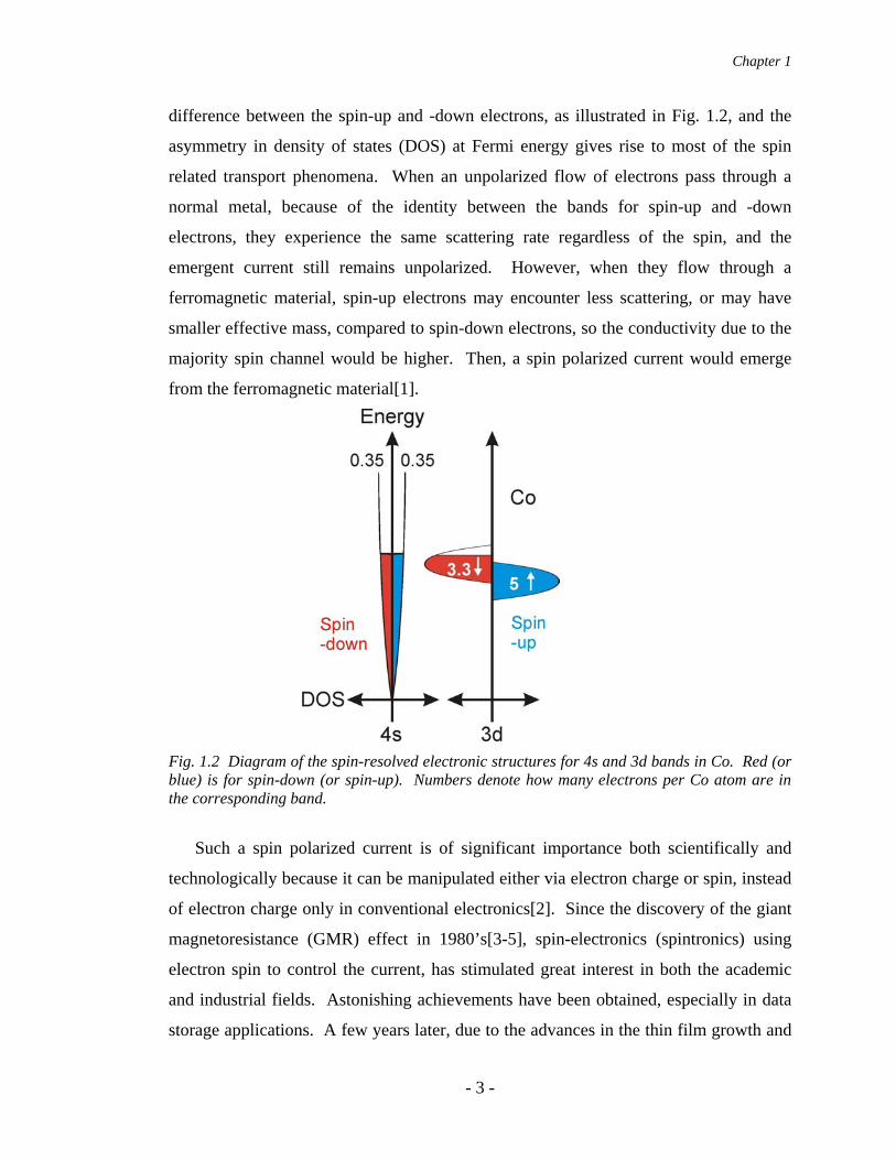
Fig. 1.2 Diagram of the spin-resolved electronic structures for 4s and 3d bands in
Co. Red (or blue) is for spin-down (or spin-up). Numbers denote how many
electrons per Co atom are in the corresponding band. . ..................................3
Chapter 2: Experimental Background
Fig. 2.1 (a) Diagrammatic structure of a MTJ with an antiferromagnetic (AF) layer
grown underneath to provide exchange bias; (b) Typical magnetoresistance
loop of a MTJ device, the inset is the minor loop. The horizontal arrows
show the magnetic moments’ directions in the two electrodes, and the
vertical arrows denote the field sweeping directions.......................................9
Fig. 2.2 Illustration of the Jullière’s model in a magnetic tunnel junction for parallel
configuration (left) and antiparallel configuration (right). The current is
determined by the product of the density of filled states in one electrode and
the density of empty states in the other electrode. Parallel configuration
usually has lower resistance than that of antiparallel configuration, thus
resulting in a positive TMR effect. ................................................................11
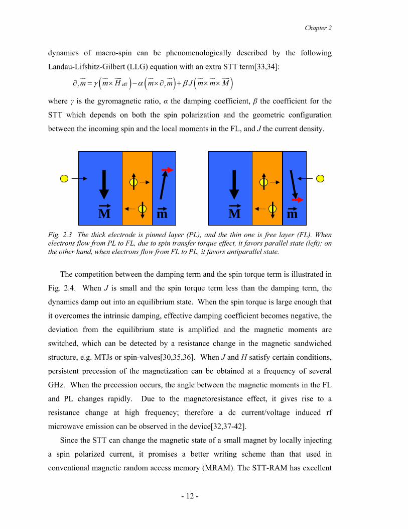
Fig. 2.3 The thick electrode is pinned layer (PL), and the thin one is free layer (FL).
When electrons flow from PL to FL, due to spin transfer torque effect, it
favors parallel state (left); on the other hand, when electrons flow from FL to
PL, it favors antiparallel state. .......................................................................12
Fig. 2.4 (a) Geometric illustration of Landau-Lifshitz-Gilbert (LLG) equation with a
spin transfer torque term; (b) Dynamics of the magnetic moments in the free
layer (FL) when the damping term is larger, comparable, or smaller than the
spin-torque term with various magnitudes of spin polarized current.… .......13
Fig. 2.5 Comparison between the conventional MRAM (left) and STT-RAM (right).
Clearly, much simpler electronic architecture is proposed for STT-RAM than
the conventional MRAM...............................................................................14
xi
List of Figures
Fig. 2.6 Superconducting-ferromagnetic-metal tunneling. (a) BCS density of states
of a superconductor as a function of voltage in a magnetic field; (b)
Temperature-dependent kernels for each spin channel in the integral
expression for differential conductance; (c) Theoretical normalized
conductance for each spin channel (dotted and dashed curves) and the total
conductance (solid line). ................................................................................17
Fig. 2.7 Schematic of the sputtering system (left); Shadow masking is used to define
the electrodes and barriers (upper middle), and blank film is grown for
lithography (lower middle); Scanning electron microscopy (SEM) images for
some devices, respectively (right)..................................................................19
Chapter 3: Enhanced Tunneling Magnetoresistance from Amorphous CoFe Alloy
Fig. 3.1 High-resolution cross-section transmission electron microscopy images of
100 Ta/250 Ir22Mn78/4 Co49Fe21BB30/35 Co70Fe30/[44 Al2O3/tSCF SCF/100
CFB]5/50 Ta/50 Ru with tSCF of 15, 20, 30, 40, and 50 Å; (a) CFB=CFB30,
as deposited; (b) high magnification of a portion of (a), together with
diffractograms of the four regions indicated by black square outlines in the
figure. These regions are taken from (bottom to top) 20 Å SCF, 100 Å
CFB30, 30 Å SCF, and 100 Å CFB30: the amorphous to crystalline
transition as a function of thickness of the SCF layer is clearly revealed; (c)
CFB=CFB10 annealed at 260 °C. The thicknesses (in Å) of the SCF, Al2O3,
and CFB layers are labeled in green, yellow, and orange, respectively. .......31
Fig. 3.2 As-deposited all-metal sample, 100 Ta/250 Ir20Mn80/100 CFB30/[tSCF=5,
10, 15, …, and 40 SCF/100 CFB30]8/50 Ta/50 Ru. The thicknesses (in Å)
of the SCF, Al2O3, and CFB30 layers are labeled in green, yellow, and
orange, respectively. ......................................................................................32
Fig. 3.3 (a) Schematic of the magnetic tunnel junction structure; (b) Major and
minor (inset) TMR loops for CFB10 samples with tSCF = 10 and 60 Å. Blue
solid and red open circles denote results after the samples are annealed at
240 °C and 300 °C, respectively....................................................................34
Fig. 3.4 Dependence of TMR on the SCF thickness at various anneal temperatures
for CFB10 (solid circle) and CFB30 (open circle) samples.… .....................35
xii
List of Figures
Fig. 3.5 Dependence of Hc on the SCF thickness at various anneal temperatures for
CFB10 (upper) and CFB30 (lower) samples.................................................36
Fig. 3.6 Dependence of TMR on anneal temperature for CFB10 (upper) and CFB30
(lower) samples with tSCF = 20 Å (red circle) and 60 Å (blue circle). The
dashed lines are guides to the eye..................................................................37
Fig. 3.7 Typical experimental data from superconducting-tunneling-spectroscopy
from the tunnel junctions with structure, 45 Al95Si5/32 Al2O3/tSCF SCF/100
CFB10/50 Ta/50 Ru, at T ~ 0.250 K and H = 2.0 T; (a) tSCF = 25 Å, as-
deposited; (b) tSCF = 25 Å, annealed at 300 °C; (c) tSCF = 70 Å, as-deposited;
(d) tSCF = 70 Å, annealed at 300 °C. Open circles are experimental data and
solid lines are fits. Δ is the fitted Al95Si5 superconducting energy gap. .......40
Fig. 3.8 Dependence of TSP on the SCF thickness at various anneal temperatures
for both CFB10 and CFB30 samples.............................................................41
Fig. 3.9 Anneal temperature dependence of TSP and resistance for both normal
(solid symbols, 45 Al95Si5/32 Al2O3/25 SCF/100 CFB30/50 Ta/50 Ru) and
inverted (open symbols, 100 Ta/250 Ir24Mn76/4 Co49Fe21BB30/35 Co70Fe30/28
Al2O3/40 Al95Si5/33 MgO) STS samples. The tunnel barrier Al2O3 was
grown by reactive sputtering in an O2-Ar mixture with (triangles) or without
an additional atomic oxygen treatment (30 or 60 seconds) after deposition.
Oxygen concentrations in the sputter gas mixture of 7% (circles and
triangles), 9% (square), and 11% (diamond) were used................................42
Fig. 3.10 Atomic force microscopy images (AFM) for Al2O3 barriers (a) in normal
structure, 45 Al95Si5/32 Al2O3; (b) in inverted structure, 100 Ta/250
Ir22Mn78/6 Co40Fe40BB20/35 Co70Fe30/32 Al2O3. Both the barriers were
deposited in the optimal condition with an Ar-O2 (93/7) mixture. Clear grains
with RMS ~ 0.395 nm in the normal structure and much smoother surface
with RMS ~ 0.190 nm in the inverted structure were observed. ...................43
Fig. 3.11 (a) Schematic diagram of the magnetic tunnel junction structure with the
SCF layer underneath the tunnel barrier; (b) Major and minor (inset) TMR
loops for tSCF = 15 Å. Black open and violet solid circles denote loops for an
xiii
List of Figures
as-deposited device and for the same device after an anneal at 260 °C,
respectively. ...................................................................................................44
Fig. 3.12 Dependence of TMR on the SCF thickness at various anneal temperatures
for the samples with CFB20 beneath Al2O3. .................................................46
Fig. 3.13 High-resolution cross-section transmission electron microscopy images
for (a) 100 Ta/250 Ir22Mn78/4 Co49Fe21BB30/5 Co70Fe30/[60 CFB20/tSCF
SCF/44 Al2O3]6 with tSCF =10, 15, 20, 30,40 and 50 Å (10 and 50 not
shown); (b) same sample as in (a) after an anneal at 260 °C. In both images,
the thicknesses of SCF, Al2O3, and CFB20 are labeled in green, yellow, and
orange, respectively. ......................................................................................47
Fig. 3.14 Fe L3 and Co L3 XES spectra as a function of the SCF thickness for 50
Ta/18 Al2O3/[tSCF SCF/20 CFB20], or 71 Co70Fe30, or 62 CFB20/10 Al2O3.
The thicknesses of CoFe (CoFeB) are shown in green (orange). The Fe and
Co 2p3/2 binding energies relative to the Fermi level are taken to be 707 eV
and 778 eV, as indicated by the dark-yellow dashed-dotted lines. ................48
Fig. 3.15 Spin-resolved s- and d- partial density of states for Fe and Co in
amorphous (blue and navy) and bcc crystalline (red and pink) Co70Fe30 alloy
structures. .......................................................................................................50
Fig. 3.16 Spin moment of each atom in the computational ensemble for amorphous
or bcc crystalline Co70Fe30. The horizontal axis indicates the label of the
individual Fe and Co atoms in the calculations. ............................................51
Chapter 4: Tunneling Anisotropic Magnetoresistance in Magnetic Tunnel Junctions
with 3d Transition Metals
Fig. 4.1 Schematic diagram of the TAMR measurement setup. Mixer adds the dc
bias voltage and a small ac voltage together, and applies the total voltage
across the tunnel junction. Lock-in amplifier is used to measure the dynamic
resistance at various dc bias voltages.............................................................62
Fig. 4.2 The bias dependence of differential conductance for the MgO (red line) and
Al2O3 (gray line) MTJs in a perpendicular field of 7 T at 10 K. The inset
shows the bias dependence of the differential TMR at 10 K.........................63
xiv
List of Figures
Fig. 4.3 Typical angular dependence of dV/dI curves for CoFe/MgO/CoFe,
CoFe/Al2O3/CoFe, and Al/MgO/Al at zero bias in a field of 7 T at 10 K.....64
Fig. 4.4 Normalized RD vs. θ curves (symbols) at various bias voltages for (a) MgO
and (b) Al2O3 MTJs. The data are displaced vertically for clarity. The solid
lines are fits using Eqs. (1) and (2).…...........................................................65
Fig. 4.5 (a) and (b) Contour plots of RD as a function of bias and angle for the MgO
and Al2O3 MTJs; (c) and (d) Corresponding contour plots of dc resistance. 67
Fig. 4.6 (a) and (b) Fitting parameters A2/A0 (solid circles) and A4/A0 (open
squares) as a function of bias for the MgO and Al2O3 MTJs. .......................68
Fig. 4.7 IETS data for the CoFe/MgO/CoFe (red line) and CoFe/Al2O3/CoFe (gray
line) MTJs after linear background subtraction. The inset shows the original
data.................................................................................................................70
Fig. 4.8 Angular dependence of the interface DOS of the majority band (in arbitrary
units) for several energies E near the resonant energy Er = −0.4 eV. Energies
are given in eV. The majority band has width 4 eV and is centered at 0.6 eV.
The width of the resonant state γ0 = 10 meV, and the spin-orbit coupling
parameter λ = 50 meV. ..................................................................................71
Fig. 4.9 Bias dependence of differential conductance for CoFe/MgO/CoFe,
CrMo/MgO/CoFe, CoFe/MgO/CrMo, and CrMo/MgO/CrMo tunnel
junctions. The insets show the I-V curves of the tunnel junctions. The
measurements were taken at 10 K in a perpendicular field of 7 T. ...............75
Fig. 4.10 Contour plots for the angular dependence of normalized dc resistance at
10 K in a field of 7 T at various bias voltages for (a) CoFe/MgO/CoFe, (b)
CrMo/MgO/CoFe, (c) CoFe/MgO/CrMo, and (d) CrMo/MgO/CrMo tunnel
junctions.........................................................................................................76
Fig. 4.11 Angular dependence of normalized resistance at 10 K in a field of 7 T at
various bias voltages for (a) CoFe/MgO/0 CoFe/CrMo, (b) CoFe/MgO/5
CoFe/CrMo, (c) CoFe/MgO/10 CoFe/CrMo, and (d) CoFe/MgO/15
CoFe/CrMo tunnel junctions. Curves are displaced vertically for clarity. ...77
Chapter 5: Spin Transfer Torque Induced Microwave Emission from MgO Based
Tunnel Junctions
xv
List of Figures
Fig. 5.1 Schematic illustration of the measurement setup for the detection of spin
transfer torque induced microware emission. ................................................86
Fig. 5.2 Transmission coefficient of microwave signals at various frequencies in the
transmission line used in the setup.................................................................87
Fig. 5.3 Circuit model of the measurement setup for the detection of spin transfer
torque induced microware emission, where Rsub is the resistance of Si
substrate underneath the electrodes, Cpad is the capacitance between electrode
and Si substrate, RMTJ is the resistance of MTJ, Coverlap is the overlap
capacitance between top contact and bottom contact which is minimized by
an extended finger..........................................................................................87
Fig 5.4 Fig 5.4 (a) R vs. H at bias voltages of 0.01, 0.50, and -0.50 V; (b) R vs. V in a
field of 530 Oe. Positive voltage corresponds to electrons flowing from pinned
layer to free layer..............................................................................................89
Fig. 5.5 Typical spectra corresponding to ±0.5 V with various fields applied along
easy axis. With large positive fields MTJ is in AP state, and with large
negative fields in P state as shown by magnetoresistance loop. ....................90
Fig. 5.6 Contour plots of spectra corresponding to ±0.5 V with various fields
applied along easy axis. Dotted white lines divide plots into P and AP state.
Black downward arrow on right shows the field sweeping direction.
Colorbar shows microwave power level in the unit of nV/Hz0.5.. .................91
Fig 5.7 Field dependence of peak frequency (open circle) and FWHM (solid
triangle) at (a) 0.50 V and (b) -0.5 V. ............................................................91
Fig. 5.8 (a) Frequency f, (b) FWHM linewidth Δf, and (c) integrated power P versus
bias voltage for the two excitation modes in antiparallel state with a magnetic
field of 236 Oe applied along easy axis. ........................................................93
Fig 5.9 (a) Field switching and (b) current induced switching of two nominally
identical devices. Magnetoresistance loops are measured at 0.01 V, and
voltage switching loops are obtained with magnetic fields applied to cancel
the dipolar coupling, or the offset field in (a), respectively. Red (blue)
curves are for Device I (II).............................................................................95
xvi
List of Figures
Fig 5.10 Microwave emission spectra for Device I (a) and II (b) at ±0.5 V with
various fields applied along easy axis. Dotted white lines divide plots into P
and AP state. Colorbar shows microwave power level in the unit of
nV/Hz0.5. Field sweeping direction is always from positive from negative. 96
Fig. 5.11 Influence of over-etching time after Co/Mn crossover in secondary ion
mass spectroscopy (SIMS) on resistance RP, TMR, coercivity Hc, and dipolar
coupling field Hoffset. ......................................................................................97
xvii

List of Figures
xviii
Chapter 1
Chapter 1
INTRODUCTION: SPIN POLARIZED CURRENT AND SPINTRONICS
- 1 -

Chapter 1
As well as mass and charge, an electron has another intrinsic property, i.e. spin angular
momentum, or simply spin. In quantum mechanics, spin is a fundamental property of
atomic nuclei and elementary particles, and is an important intrinsic degree of freedom.
Although as the name indicates spin was originally thought of particles spinning around
their own axis, it had been shown by Dirac that electron spin arises naturally within
relativistic quantum mechanics. The component of electron spin measured along any
direction can only take on the values,
, 1z zs s / 2= ±Z
Namely, in a classical picture, electron spin can only point to up or down along a
magnetic field which can be vividly illustrated by a small magnet with its north pole
pointing to up or down as shown in Fig. 1.1. The intrinsic magnetic dipole moment
associated with such a spin in an electron is very close to a universal constant called the
Bohr magneton, ( ) ( )23 2 200.927 10 / 0.927 10 /2B
e
e J T or A m erg Oem
μ − −= = × ⋅ = ×Z .
Fig. 1.1 Classical illustration of electron spin as a small magnet with north pole pointing to up or down.
In normal materials, such as Cu, Ag, etc., spin-up and -down electrons are equally
populated and randomly distributed in an equilibrium state. However, in some solids
due to the quantum mechanical exchange interaction, electron spins are aligned
spontaneously, resulting in unequal numbers of spin-up and -down electrons, therefore
ferromagnetic materials are formed, such as Co, Fe, Ni, and many of their alloys. In
these ferromagnetic materials, spin-resolved electronic structures show the band
- 2 -
Chapter 1
difference between the spin-up and -down electrons, as illustrated in Fig. 1.2, and the
asymmetry in density of states (DOS) at Fermi energy gives rise to most of the spin
related transport phenomena. When an unpolarized flow of electrons pass through a
normal metal, because of the identity between the bands for spin-up and -down
electrons, they experience the same scattering rate regardless of the spin, and the
emergent current still remains unpolarized. However, when they flow through a
ferromagnetic material, spin-up electrons may encounter less scattering, or may have
smaller effective mass, compared to spin-down electrons, so the conductivity due to the
majority spin channel would be higher. Then, a spin polarized current would emerge
from the ferromagnetic material[1].
Fig. 1.2 Diagram of the spin-resolved electronic structures for 4s and 3d bands in Co. Red (or blue) is for spin-down (or spin-up). Numbers denote how many electrons per Co atom are in the corresponding band.
Such a spin polarized current is of significant importance both scientifically and
technologically because it can be manipulated either via electron charge or spin, instead
of electron charge only in conventional electronics[2]. Since the discovery of the giant
magnetoresistance (GMR) effect in 1980’s[3-5], spin-electronics (spintronics) using
electron spin to control the current, has stimulated great interest in both the academic
and industrial fields. Astonishing achievements have been obtained, especially in data
storage applications. A few years later, due to the advances in the thin film growth and
- 3 -
Chapter 1
device fabrication, an even more significant effect, called the tunneling
magnetoresistance (TMR) effect, was observed at room temperature in magnetic
tunneling junctions (MTJs)[6-9]. Because of their huge TMR and high resistance,
MTJs promise attractive applications in magnetic field sensor and magnetic random
access memory (MRAM) in very small scale of solid-state circuitry[2]. Read heads
with MTJs in hard disk are commercially available, and there are many ongoing efforts
to realize MRAM. This new type of memory has all the key desirable attributes
required by the ever growing demand for storing and processing the explosive amount
of information, such as fast access times, non-volatility, lower power-consumption, and
high density. Moreover, from the perspective of physics, the quantum mechanical
tunneling process in MTJs is not only very interesting but also extremely complicated,
and many issues about it remain poorly understood[10].
The focus of the research in this dissertation is to deepen the understanding of the
spin dependent tunneling effect in MTJs. A brief background in MTJs is provided in
Chapter 2. It is first shown in Chapter 3 that the normally crystalline CoFe can be made
amorphous when sandwiched between two amorphous layers, and when this amorphous
CoFe is incorporated as an electrode in MTJs it gives rise to an enhanced TMR
compared to its crystalline counterpart. The tunneling anisotropic magnetoresistance
(TAMR) effect is investigated in conventional MTJs in Chapter 4, and it is found that
the angular dependence of the TAMR effect shows complex two-fold and four-fold
symmetry evolution with bias voltage. Chapter 5 is devoted to the studies of the current
induced switching and microwave emission from MTJs due to the spin transfer torque
effect. Chapter 6 provides a summary of the dissertation and some suggestions for
future research.
- 4 -
Chapter 1
REFERENCES:
[1] R. C. O'Handley, "Modern Magnetic Materials: Principles and Applications,"
(John Wiley & Sons, 2000).
[2] S. Parkin, X. Jiang, C. Kaiser, A. Panchula, K. Roche, and M. Samant,
"Magnetically Engineered Spintronic Sensors and Memory," Proc. IEEE 91, 661
(2003).
[3] M. N. Baibich, J. M. Broto, A. Fert, F. N. Van Dau, F. Petroff, P. Etienne, G.
Creuzet, A. Friederich, and J. Chazelas, "Giant Magnetoresistance of
(001)Fe/(001)Cr Magnetic Superlattices," Phys. Rev. Lett. 61 (21), 2472 (1988).
[4] G. Binasch, P. Grunberg, F. Saurenbach, and W. Zinn, "Enhanced
magnetoresistance in layered magnetic structures with antiferromagnetic
interlayer exchange," Phys. Rev. B 39 (7), 4828 (1989).
[5] S. S. P. Parkin, N. More, and K. P. Roche, "Oscillations in exchange coupling
and magnetoresistance in metallic superlattice structures: Co/Ru, Co/Cr, and
Fe/Cr," Phys. Rev. Lett. 64 (19), 2304 (1990).
[6] M. Julliere, "Tunneling between ferromagnetic films," Phys. Lett. A 54, 225
(1975).
[7] J. S. Moodera, L. R. Kinder, T. M. Wong, and R. Meservey, "Large
Magnetoresistance at Room Temperature in Ferromagnetic Thin Film Tunnel
Junctions," Phys. Rev. Lett. 74, 3273 (1995).
[8] S. S. P. Parkin, C. Kaiser, A. F. Panchula, P. Rice, M. G. Samant, S.-H. Yang,
and B. Hughes, "Giant tunneling magnetoresistance at room temperature with
MgO (100) tunnel barriers," Nature Materials 3, 862 (2004).
[9] S. Yuasa, T. Nagahama, A. Fukushima, Y. Suzuki, and K. Ando, "Giant room-
temperature magnetoresistance in single-crystal Fe/MgO/Fe magnetic tunnel
junctions," Nature Materials 3, 868 (2004).
[10] E. Y. Tsymbal, O. N. Mryasov, and P. R. LeClair, "Spin-dependent tunnelling in
magnetic tunnel junctions," J. Phys. C: Condens. Matter 15, R109 (2003).
- 5 -
Chapter 1
- 6 -
Chapter 2
Chapter 2
EXPERIMENTAL BACKGROUND
- 7 -
Chapter 2
2.1 SPIN POLARIZED CURRENT IN MAGNETIC TUNNEL JUNCTIONS
Magnetic tunnel junctions (MTJs) are sandwiched heterostructures, composed of two
ferromagnetic electrodes and an ultrathin insulator barrier in between, and present many
interesting phenomena that are important for both the exploration of underlying physics
and the applications in technology[1]. When electrons flow through a MTJ, they
become spin-polarized by the first magnetic electrode. Thereafter, the interplay
between the spin-polarized current and the second magnetic layer manifests itself via
two effects, i.e. tunneling magnetoresistance effect and spin transfer torque effect. In
the current section of this chapter, brief reviews will be given on these two interesting
effects.
2.1.1 Tunneling Magnetoresistance
The resistance of a MTJ depends on the relative alignment of the magnetic moments in
the ferromagnetic electrodes. Usually, when the moments are parallel the tunneling
resistance is low; when anti-parallel, the resistance is high, thus giving rise to a
tunneling magnetoresistance (TMR) effect,
100%AP P
P
R RTMRR−
= × ,
where RAP and RP are the resistances for the parallel and anti-parallel configurations. A
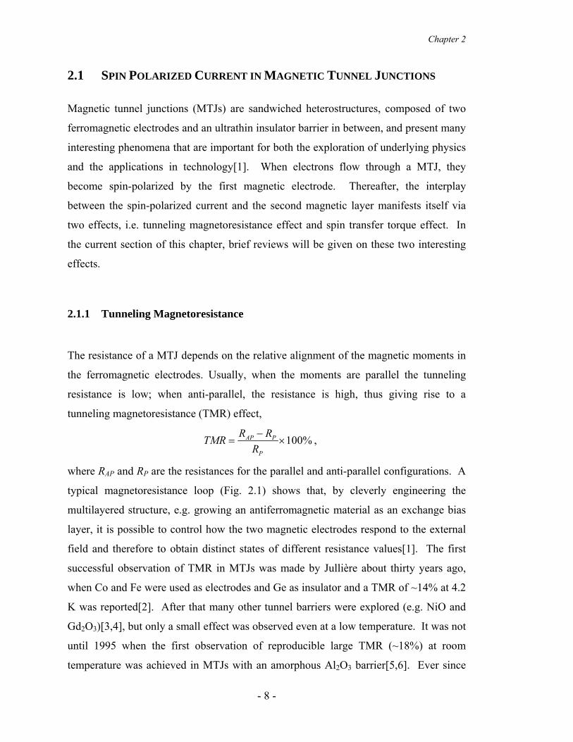
typical magnetoresistance loop (Fig. 2.1) shows that, by cleverly engineering the
multilayered structure, e.g. growing an antiferromagnetic material as an exchange bias
layer, it is possible to control how the two magnetic electrodes respond to the external
field and therefore to obtain distinct states of different resistance values[1]. The first
successful observation of TMR in MTJs was made by Jullière about thirty years ago,
when Co and Fe were used as electrodes and Ge as insulator and a TMR of ~14% at 4.2
K was reported[2]. After that many other tunnel barriers were explored (e.g. NiO and
Gd2O3)[3,4], but only a small effect was observed even at a low temperature. It was not
until 1995 when the first observation of reproducible large TMR (~18%) at room
temperature was achieved in MTJs with an amorphous Al2O3 barrier[5,6]. Ever since
- 8 -
Chapter 2
then, MTJs have aroused considerable interest due to their potential applications in
spintronic devices, such as high-performance solid-state magnetic random access
memories (MRAM) and magnetic sensors[1].
Pinned FM
Free FM
AF -100 -50 0 500
20
40
60
80
-800 -600 -400 -200 0 2000
20
40
60
80
H (Oe)
TMR
(%)
TMR
(%)
H (Oe)
(a) (b)
Fig. 2.1 (a) Diagrammatic structure of a MTJ with an antiferromagnetic (AF) layer grown underneath to provide exchange bias; (b) Typical magnetoresistance loop of a MTJ device, the inset is the minor loop. The horizontal arrows show the magnetic moments’ directions in the two electrodes, and the vertical arrows denote the field sweeping directions.
Over the past ten years, most of the research in spin dependent tunneling has
focused on MTJs with an Al2O3 tunnel barrier[7-9]. Although intensive efforts have
been made in such MTJs, the maximum TMR only reached about 70%[10,11].
Meanwhile, extensive theoretical and experimental work has been carried out to
increase the TMR by incorporating exotic oxide or half-metal layers into MTJs[12-15],
and studying crystalline tunneling barriers[16,17]. Butler et al. carried out first-
principles calculations of tunneling conductance and magnetoresistance in epitaxial
Fe/MgO/Fe sandwiches[16]. They revealed that tunneling conductance depends
strongly on the symmetry of the Bloch states in the electrodes and of the evanescent
states in the barrier, thus Bloch states of different symmetry decay at different rates
within the barrier. The state, due to its “s-character”, decays slowest among all the
states and can make a significant contribution to the tunneling conductance. Because
the state only occurs at the Fermi level for the majority band, it behaves much like a
“half-metal”. Giant TMR was expected in bcc Fe/MgO/Fe, CoFe/MgO/CoFe, and
Co/MgO/Co tunneling junctions. Experimental results of TMR above ~200% were first
1Δ
1Δ
- 9 -
Chapter 2
reported by Parkin et al. and Yuasa et al. respectively[18,19]. Room temperature TMR
results of about 600% in MgO based tunnel junctions have also been obtained
recently[20].
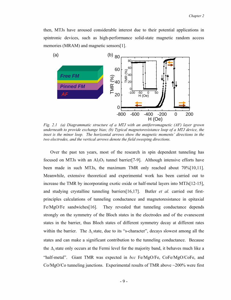
For high-quality Al2O3 tunnel junctions, the magnitude of the TMR at low bias can
be well understood within the framework of Jullière’s model, 1 2
1 2
21
PPTMRPP
=−
, where
P1, P2 are the spin polarization of the two electrode materials and they can be well
derived from the ferromagnet/insulator/superconducting tunnel junctions first
introduced by Meservy and Tedrow[21]. In this model, it is assumed that during the
tunneling process, spin is conserved, namely no spin-flipping occurs. The conductance
in each channel is thus proportional to the tunneling probability, which is determined by
Fermi’s golden rule (Fig. 2.2). However, such a quantitative comparison is not always
straightforward. For example, TMR is extremely sensitive to the interface between the
electrode and barrier in realistic systems[22,23]. In MgO based MTJs, due to coherent
tunneling effect, the physics of the spin dependent tunneling effect is far beyond this
oversimplified model. Given the simplicity of the model, Slonczewski calculated an
approximate expression of the TMR of free electrons tunneling through a square barrier
based on the Landauer-Büttiker formalism[24]. Tsymbal et al. studied the interface
dependence of the tunneling conductance[23]. For the coherent tunneling through a
crystalline system many theoretical studies emerged together with the experimental
achievements in MgO based tunnel junctions[16-19].
In conventional MTJs, TMR always decreases with applied bias voltage. The
voltage at which the magnitude decreases to half of the low bias value is called V1/2,
usually around 0.5 V for high quality Al2O3 or MgO based MTJs with transition metal
electrodes[11,19]. The TMR decrease mainly comes from the much greater resistance
drop in the anti-parallel (AP) state with bias voltage compared to the parallel (P) state.
One mechanism for the decrease in TMR as a function of bias is the interface magnon
excitation[25]. Another is the presence of defect states within the tunnel barrier, which
may allow an increase amount of defect-state-assisted tunneling and dilute the spin
polarization of the tunneling current at elevated bias voltage[26,27].
- 10 -
Chapter 2
E E
NS N SE F E
F
EF
EF
e e
FM FMF FI I
M MM M
Ima ImajImin Imin
21 1 2AP N NI N N↓ ↓↑ ↑↑ ↑ ∝ +1 2 1 2
PI NN N N↓ ↓∝ +
Fig. 2.2 Illustration of the Jullière’s model in a magnetic tunnel junction for parallel configuration (left) and antiparallel configuration (right). The current is determined by the product of the density of filled states in one electrode and the density of empty states in the other electrode. Parallel configuration usually has lower resistance than that of antiparallel configuration, thus resulting in a positive TMR effect.
2.1.2 Spin Transfer Torque
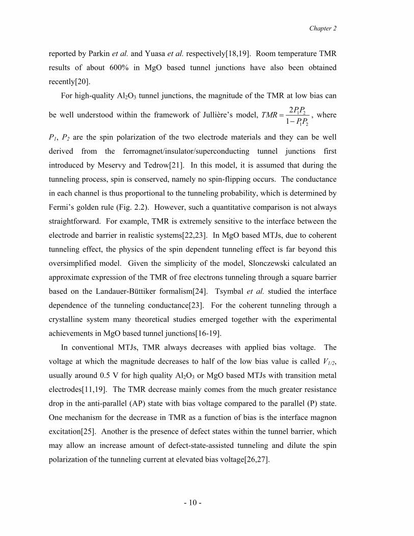
Spin transfer torque (STT) effect was first theoretically studied by Slonczewski and
Berger in 1996[28,29]. When a spin-polarized current pass through a non-collinear thin
magnetic layer, due to the conservation of the spin momentum via exchange interaction,
the transverse component of the spin in the flowing electrons can be transferred to the
conduction electrons in the small magnet. Depending on the direction of electron flow
and the magnetic configuration, this spin-polarized current favors either the P state or
AP state (Fig. 2.3). The electrode of smaller thickness, which can be switched, is called
the free layer (FL); in contrast, the other electrode, which is usually thicker and
exchange biased, is called pinned layer (PL). Such a STT induced magnetization
reversal is a relatively new phenomenon, and it is observable only in magnetic
structures smaller than 100-200 nm[30-32]. A macro-spin model treats a nanomagnet
with the assumption that its internal magnetic degrees of freedom are frozen, so that the
- 11 -
Chapter 2
dynamics of macro-spin can be phenomenologically described by the following
Landau-Lifshitz-Gilbert (LLG) equation with an extra STT term[33,34]:
( ) ( ) ( )efft tm m H m m J m m Mγ α β∂ = × − ×∂ + × ×gd gd ggd gd gd gd gd ggd
where γ is the gyromagnetic ratio, α the damping coefficient, β the coefficient for the
STT which depends on both the spin polarization and the geometric configuration
between the incoming spin and the local moments in the FL, and J the current density.
Fig. 2.3 The thick electrode is pinned layer (PL), and the thin one is free layer (FL). When electrons flow from PL to FL, due to spin transfer torque effect, it favors parallel state (left); on the other hand, when electrons flow from FL to PL, it favors antiparallel state.
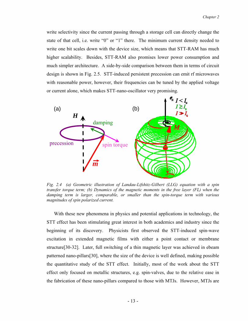
The competition between the damping term and the spin torque term is illustrated in
Fig. 2.4. When J is small and the spin torque term less than the damping term, the
dynamics damp out into an equilibrium state. When the spin torque is large enough that
it overcomes the intrinsic damping, effective damping coefficient becomes negative, the
deviation from the equilibrium state is amplified and the magnetic moments are
switched, which can be detected by a resistance change in the magnetic sandwiched
structure, e.g. MTJs or spin-valves[30,35,36]. When J and H satisfy certain conditions,
persistent precession of the magnetization can be obtained at a frequency of several
GHz. When the precession occurs, the angle between the magnetic moments in the FL
and PL changes rapidly. Due to the magnetoresistance effect, it gives rise to a
resistance change at high frequency; therefore a dc current/voltage induced rf
microwave emission can be observed in the device[32,37-42].
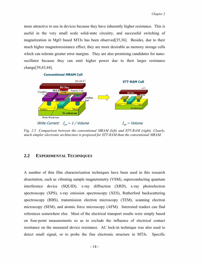
Since the STT can change the magnetic state of a small magnet by locally injecting
a spin polarized current, it promises a better writing scheme than that used in
conventional magnetic random access memory (MRAM). The STT-RAM has excellent
mM M m
- 12 -
Chapter 2
write selectivity since the current passing through a storage cell can directly change the
state of that cell, i.e. write “0” or “1” there. The minimum current density needed to
write one bit scales down with the device size, which means that STT-RAM has much
higher scalability. Besides, STT-RAM also promises lower power consumption and
much simpler architecture. A side-by-side comparison between them in terms of circuit
design is shown in Fig. 2.5. STT-induced persistent precession can emit rf microwaves
with reasonable power, however, their frequencies can be tuned by the applied voltage
or current alone, which makes STT-nano-oscillator very promising.
Fig. 2.4 (a) Geometric illustration of Landau-Lifshitz-Gilbert (LLG) equation with a spin transfer torque term; (b) Dynamics of the magnetic moments in the free layer (FL) when the damping term is larger, comparable, or smaller than the spin-torque term with various magnitudes of spin polarized current.
With these new phenomena in physics and potential applications in technology, the
STT effect has been stimulating great interest in both academics and industry since the
beginning of its discovery. Physicists first observed the STT-induced spin-wave
excitation in extended magnetic films with either a point contact or membrane
structure[30-32]. Later, full switching of a thin magnetic layer was achieved in ebeam
patterned nano-pillars[30], where the size of the device is well defined, making possible
the quantitative study of the STT effect. Initially, most of the work about the STT
effect only focused on metallic structures, e.g. spin-valves, due to the relative ease in
the fabrication of these nano-pillars compared to those with MTJs. However, MTJs are
damping
spin torque precession
H (a) (b)
m
- 13 -
Chapter 2
more attractive to use in devices because they have inherently higher resistance. This is
useful in the very small scale solid-state circuitry, and successful switching of
magnetization in MgO based MTJs has been observed[35,36]. Besides, due to their
much higher magnetoresistance effect, they are more desirable as memory storage cells
which can tolerate greater error margins. They are also promising candidates for nano-
oscillator because they can emit higher power due to their larger resistance
uch simpler electronic architecture is proposed for STT-RAM than the conventional MRAM.
.2 EXPERIMENTAL TECHNIQUES
change[39,43,44].
ig. 2.5 Comparison between the conventional MRAM (left) and STT-RAM (right). Clearly,F
m
2
A number of thin film characterization techniques have been used in this research
dissertation, such as vibrating sample magnetometry (VSM), superconducting quantum
interference device (SQUID), x-ray diffraction (XRD), x-ray photoelectron
spectroscopy (XPS), x-ray emission spectroscopy (XES), Rutherford backscattering
spectroscopy (RBS), transmission electron microscopy (TEM), scanning electron
microscopy (SEM), and atomic force microscopy (AFM). Interested readers can find
references somewhere else. Most of the electrical transport results were simply based
on four-point measurements so as to exclude the influence of electrical contact
resistance on the measured device resistance. AC lock-in technique was also used to
detect small signal, or to probe the fine electronic structure in MTJs. Specific
- 14 -
Chapter 2
experimental setups for the different experiments will be discussed later in the
respective chapters. However, one special technique, i.e. superconducting tunneling
spectroscopy, will be described in details in this section due to its theoretical and
xperimental complexities.
.2.1 Superconducting Tunneling Spectroscopy
3d
tran
nneling electrons from left electrode to
right electrode at energy E and vice versus are,
e
2
Spin polarization is a crucial metric for all spin related phenomena. It can be probed by
a variety of techniques, such as photoemission[45], point contact Andreev
reflection[46], and superconducting tunneling spectroscopy (STS)[21]. Regarding the
spin dependent tunneling effect in MTJs, STS is the most reliable and relevant
technique to determine the tunneling spin polarization (TSP). In this technique, TSP is
measured from a tunnel junction with an electrode of the interested material and a
counter electrode of a superconducting material. Slightly doped aluminum with copper
or silicon is commonly used as the superconducting electrode, where the doping can
increase the critical temperature Tc of the superconductor. With a large field applied in
the film plane, the superconducting electrode works as an analyzer for the spin-
polarized current. This technique was first developed by Meservey and Tedow, and has
been used to measure many ferromagnetic and ferromagnetic materials including
sition metals and their alloys and some rare-earth metal based alloys[21,47,48].
When a bias voltage is applied across the tunnel junction, the initially aligned Fermi
levels in the two electrodes are shifted, therefore giving rise to a tunneling current.
According to Fermi’s golden rule, the current that is directly correlated with the
tunneling probability, is determined by the product of the density of filled states of a
given energy in one electrode and the density of empty states at the same energy in the
other electrode. By this rule, the currents of tu
( ) ( ) ( ) ( ) ( )( ) ( ) ( ) ( ) (
1 2
1 2
, ~ 1
, ~ 1 )I V E N E eV N E f E eV f E
I V E N E eV N E f E eV f E+
−
+ + −⎡ ⎤⎣ ⎦+ − +⎡ ⎤⎣ ⎦
- 15 -
Chapter 2
respectively, where V is the applied voltage, N1,2 are the density of states of the two
electrodes, and f is the Fermi function. Thus the total current I, given by
( ) ( ), ,I V E I V E dE+∞
+ −−∞−∫ , is equal to,
( ) ( ) ( ) ( ) ( )1 2~I V N E eV N E f E eV f E+∞
−∞+ + − dE⎡ ⎤⎣ ⎦∫
For a non-magnetic metal, we can assume the density of sates around the Fermi energy
within a small range is constant; however, a superconductor behaves differently.
Therefore, the integration must be carried out over it, and the differential conductance
can be easily derived,
( ) ( ) ( )~ n s
dI VN N E f E eV d
dV+∞
−∞′ +∫ E
For the case of tunneling from a magnetic material, when we calculate the conductance
we must consider both the spin-up and spin-down channels.
( ) ( ) ( ) ( ) ( )~ s s
dI VN N E f E eV dE N N E f E eV d
dV+∞ +∞
↑ ↑ ↓ ↓−∞ −∞′ ′+ + +∫ ∫ E
Where the spin conservation is assumed during the tunneling process, and and ( )N↑ ↓
( )s sN↑ ↓
are the spin-up (spin-down) density of states in the magnetic materials and in the
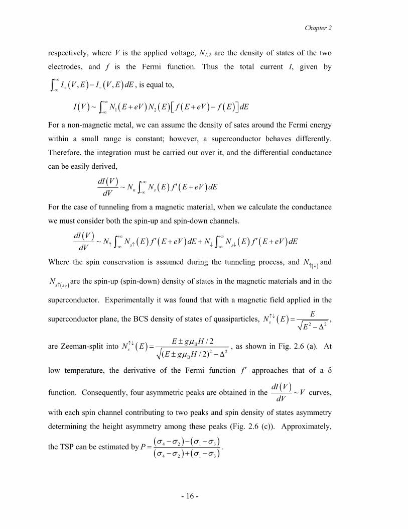
superconductor. Experimentally it was found that with a magnetic field applied in the
superconductor plane, the BCS density of states of quasiparticles, ( )2 2sEN E
E↑↓ =
− Δ,
are Zeeman-split into ( ) B2 2
B
/ 2( / 2)
sE g HN E
E g Hμ
μ↑↓ ±
=± −Δ
, as shown in Fig. 2.6 (a). At
low temperature, the derivative of the Fermi function f ′ approaches that of a δ
function. Consequently, four asymmetric peaks are obtained in the ( ) ~dI V
VdV
curves,
with each spin channel contributing to two peaks and spin density of states asymmetry
determining the height asymmetry among these peaks (Fig. 2.6 (c)). Approximately,
the TSP can be estimated by ( ) ( )( ) ( )
4 2 1 3
4 2 1 3
Pσ σ σ σσ σ σ σ
− − −=
− + −.
- 16 -
Chapter 2
Fig. 2.6 Superconducting-ferromagnetic-metal tunneling[21]. (a) BCS density of states of a superconductor as a function of voltage in a magnetic field; (b) Temperature-dependent kernels for each spin channel in the integral expression for differential conductance; (c) Theoretical normalized conductance for each spin channel (dotted and dashed curves) and the total conductance (solid line).
In the simple BCS theory, neither the orbital depairing due to the applied field nor
spin-flip scattering due to the spin-orbit coupling (SOC) is included. A more
complicated DOS calculation was completed by Maki after taking these factors into
account[49,50],
( ) ( ) ( )( )1/ 22
0sgn Re
2 1s
s
N uN E Eu
↑↓ ±
±
⎛ ⎞⎜ ⎟=⎜ ⎟−⎝ ⎠
where u and u are implicitly defined by + − ( ) ( )1/ 2 1/ 22 21 1B u uE H uu b
u u
μ ς ±±±
±
⎛ ⎞−⎜ ⎟= + +⎜ ⎟Δ − −⎝ ⎠
∓
∓
∓ ,
is the energy gap of the superconductor, Δ ( )0sN is the normal density of states, ς is
the orbital depairing parameter, and b is the spin-orbit scattering parameter[51], In
each experiment with applied field and temperature known, the conductance curve is fit
- 17 -
Chapter 2
by Maki’s theory with , Δ ς , b and TS as fitting parameters. The TSP results can be
derived with high accuracy[52]. One of our typical TSP measurements and analysis are
shown in Fig. 3.7.
P
2.3 DEVICE PREPARATION All the films grown for the research are deposited on thermally oxidized 1-inch Si
wafers. The deposition system is equipped with several dc magnetron sputtering guns, a
plasma oxidation source, and an ion beam sputter source with a five target turret and an
electron-beam evaporation source shown in Fig. 2.7. Every time after opening the
chamber and loading cleaned Si substrates, the system is usually baked for 8~10 hours
at 120 °C, and the chamber thereafter reaches a base pressure of better than 10-8 Torr.
With the capacity of 24 substrates, any gas mixture among Ar, O2 and N2, and more
than 11 targets, the system allows to explore materials intensively and to optimize
structures efficiently.
The deposition conditions vary depending on the desired materials. Metallic films
are usually deposited with an Ar atmosphere at a pressure of 3 mTorr, and oxide
barriers are normally grown by reactive sputtering in an Ar/O2 mixture with an optimal
ratio between 97/3 and 95/5. Small permanent magnets with a field about 100 Oe are
placed above the substrate to set the moments direction in magnetic layer, especially to
establish the exchange bias.
There are two ways to make the final measurable devices: one is directly patterning
the film with in situ shadow masks; the other is patterning the devices from uniformly
deposited films using optical or ebeam lithography in a clean room. (Fig. 2.7)
2.3.1 Shadow Masked Devices
The film deposition and device patterning process is fully automated by computer. By
controlling a motor inside the chamber, both the substrate platter and the mask platter
- 18 -
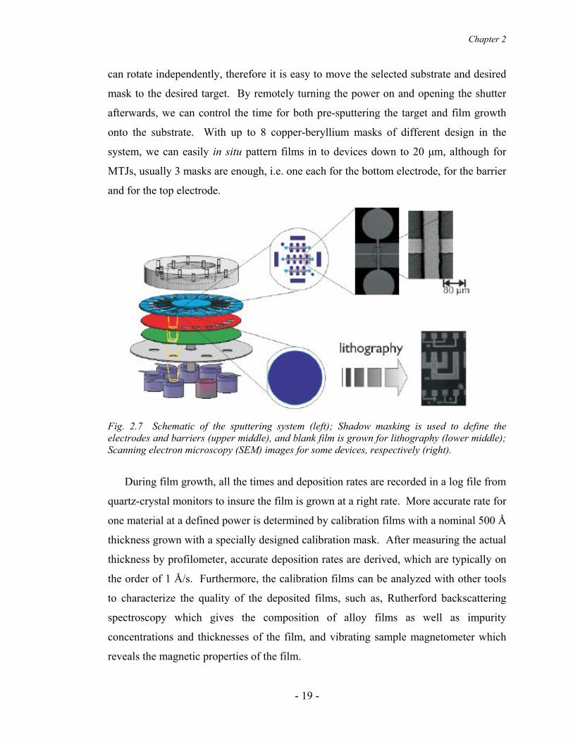
Chapter 2
can rotate independently, therefore it is easy to move the selected substrate and desired
mask to the desired target. By remotely turning the power on and opening the shutter
afterwards, we can control the time for both pre-sputtering the target and film growth
onto the substrate. With up to 8 copper-beryllium masks of different design in the
system, we can easily in situ pattern films in to devices down to 20 μm, although for
MTJs, usually 3 masks are enough, i.e. one each for the bottom electrode, for the barrier
and for the top electrode.
Fig. 2.7 Schematic of the sputtering system (left); Shadow masking is used to define the electrodes and barriers (upper middle), and blank film is grown for lithography (lower middle); Scanning electron microscopy (SEM) images for some devices, respectively (right).
During film growth, all the times and deposition rates are recorded in a log file from
quartz-crystal monitors to insure the film is grown at a right rate. More accurate rate for
one material at a defined power is determined by calibration films with a nominal 500 Å
thickness grown with a specially designed calibration mask. After measuring the actual
thickness by profilometer, accurate deposition rates are derived, which are typically on
the order of 1 Å/s. Furthermore, the calibration films can be analyzed with other tools
to characterize the quality of the deposited films, such as, Rutherford backscattering
spectroscopy which gives the composition of alloy films as well as impurity
concentrations and thicknesses of the film, and vibrating sample magnetometer which
reveals the magnetic properties of the film.
- 19 -
Chapter 2
2.3.2 Nano-Pillar Devices
Devices used for the STT studies are fabricated by ebeam lithography and standard
optical lithography. Films were grown with the same technique, however, without use
of any shadow masks. Before being brought into the clean room, samples are usually
annealed at an optimal condition, which is determined by the thermal stability and TMR
of the shadow-masked larger devices with identical multilayered structures. It takes
four major steps to fabricate the devices with a size of ~100 nm.
(i). Alignment Mark. Bilayers of photoresist (SPR670 600nm/PMGI-SFG 50nm)
are used in this step to make an undercut for ease of later liftoff. After the resists spin
and bake, they are exposed with an alignment mark mask for 1.5 seconds with 1000 W
in a contact printer. Develop the exposed resist in Optiyield developer for 45 seconds,
and deposit Ta 5 nm/Au 65 nm metal layers where thin Ta is used to increase the
adhesion. Finally, dissolve the resist with NMP and liftoff the metal, which generates
four alignment marks with size of 10×10 μm2 at each of the four corners across the
wafer.
(ii). Device Region and Bottom Electrode. Device fabrication regions with full
stack of the film are defined by ebeam lithography. After resist spinning, exposing and
developing, resist islands with bottom electrode shape remain on the wafer. Using the
resist as a hard mask, the rest of the metal layers are ion-milled to etch through the
whole film stack, thus a matrix of separated regions for later device fabrication is
formed. This process is precisely monitored by secondary ion mass spectroscopy
(SIMS). After a complete etching, Al2O3 of the same thickness as the totally etched
layers is deposited in situ by ion beam deposition (IBD). Liftoff with swabbing and
ultrasonic agitation in N-Methyl-2-Pyrrolidone (NMP), the device fabrication regions
and bottom electrodes are defined.
(iii). Tunnel Junction. Small junctions of sizes from 50×100 to 90×270 nm2 are
fabricated by ebeam lithography. Bialyers of ebeam resist (HSQ 85 nm/Duramide 40
nm) are spun onto the substrate, with each of them baked at 100 °C and 175 °C for 30
seconds. After developing, HSQ resist islands with the desired tunnel junction shape
and size remain on the wafer. Oxygen reactive ion etching treatment transfers the HSQ
- 20 -
Chapter 2
pattern onto Duramide, which also creates a slight undercut there. With HSQ/Duramide
as a hard mask, an ion-mill is used to etch through the film to the pinned ferromagnetic
layer. The ion beam starts with an incident angle between 0 to 10 degrees from
perpendicular to the surface, followed by a sidewall cleaning roughly with 2× time of
the etching. The un-etched bottom layers beneath tunneling barrier serve as bottom
electrode, and small pillars defined by the resist islands are the active tunnel junctions.
Al2O3 is then deposited with the same thickness as the etched depth. After liftoff, small
holes on top of the pillars, namely tunnel junctions, are opened for making top
electrodes.
(iv). Electrical Contact. The surface is first de-scummed with O2 plasma for 40
seconds with a pressure of 500 Torr, and then the contact metal (Ta 5 nm/Au 180 nm) is
deposited. After resist spinning, exposing, and developing, the patterns of both the top
and bottom contacts are defined. Ion-mill is used to etch away the rest of the Ta/Au
stack, and the electrical contacts are generated. Finally, resist is removed by swabbing
and ultrasonic agitation with NMP.
- 21 -
Chapter 2
REFERENCES:
[1] S. Parkin, X. Jiang, C. Kaiser, A. Panchula, K. Roche, and M. Samant,
"Magnetically Engineered Spintronic Sensors and Memory," Proc. IEEE 91, 661
(2003).
[2] M. Julliere, "Tunneling between ferromagnetic films," Phys. Lett. A 54, 225
(1975).
[3] S. Maekawa and U. Gafvert, "Electron tunneling between ferromagnetic films,"
IEEE Trans. Magn. 18, 707 (1982).
[4] J. Nowak and J. Rauluszkiewicz, "Spin dependent electron tunneling between
ferromagnetic films," J. Magn. Magn. Mater. 109, 79 (1992).
[5] T. Miyazaki and N. Tezuka, "Giant magnetic tunneling effect in Fe/Al2O3/Fe
junction," J. Magn. Magn. Mater. 139, L231 (1995).
[6] J. S. Moodera, L. R. Kinder, T. M. Wong, and R. Meservey, "Large
Magnetoresistance at Room Temperature in Ferromagnetic Thin Film Tunnel
Junctions," Phys. Rev. Lett. 74, 3273 (1995).
[7] P. LeClair, J. T. Kohlhepp, C. H. van de Vin, H. Wieldraaijer, H. J. M. Swagten,
W. J. M. de Jonge, A. H. Davis, J. M. MacLaren, J. S. Moodera, and R. Jansen,
"Band Structure and Density of States Effects in Co-Based Magnetic Tunnel
Junctions," Phys. Rev. Lett. 88, 107201 (2002).
[8] J. S. Moodera, J. Nowak, and R. J. M. van de Veerdonk, "Interface Magnetism
and Spin Wave Scattering in Ferromagnet-Insulator-Ferromagnet Tunnel
Junctions," Phys. Rev. Lett. 80, 2941 (1998).
[9] S. Yuasa, T. Nagahama, and Y. Suzuki, "Spin-Polarized Resonant Tunneling in
Magnetic Tunnel Junctions," Science 297, 234 (2002).
[10] D. Wang, C. Nordman, J. M. Daughton, Z. Qian, and J. Fink, "70% TMR at
Room Temperature for SDT Sandwich Junctions With CoFeB as Free and
Reference Layers," IEEE Trans. Magn. 40, 2269 (2004).
[11] J. J. Yang, C. Ji, Y. A. Chang, X. Ke, and M. S. Rzchowski, "Over 70%
tunneling magnetoresistance at room temperature for a CoFe and AlOx based
magnetic tunnel junction," Appl. Phys. Lett. 89, 202502 (2006).
- 22 -
Chapter 2
[12] A. M. Bratkovsky, "Tunneling of electrons in conventional and half-metallic
systems: Towards very large magnetoresistance," Phys. Rev. B 56, 2344 (1997).
[13] A. M. Bratkovsky, "Assisted tunneling in ferromagnetic junctions and half-
metallic oxides," Appl. Phys. Lett. 72, 2334 (1998).
[14] J. M. De Teresa, Barth, eacute, A. my, egrave, A. Fert, J. P. Contour, F.
Montaigne, ccedil, ois, and P. Seneor, "Role of Metal-Oxide Interface in
Determining the Spin Polarization of Magnetic Tunnel Junctions," Science 286,
507 (1999).
[15] C. T. Tanaka, J. Nowak, and J. S. Moodera, "Spin-polarized tunneling in a half-
metallic ferromagnet," J. Appl. Phys. 86, 6239 (1999).
[16] W. H. Butler, X.-G. Zhang, T. C. Schulthess, and J. M. MacLaren, "Spin-
dependent tunneling conductance of Fe|MgO|Fe sandwiches," Phys. Rev. B 63,
054416 (2001).
[17] J. Mathon and A. Umerski, "Theory of tunneling magnetoresistance of an
epitaxial Fe/MgO/Fe(001) junction," Phys. Rev. B 63, 220403 (2001).
[18] S. S. P. Parkin, C. Kaiser, A. F. Panchula, P. Rice, M. G. Samant, S.-H. Yang,
and B. Hughes, "Giant tunneling magnetoresistance at room temperature with
MgO (100) tunnel barriers," Nature Materials 3, 862 (2004).
[19] S. Yuasa, T. Nagahama, A. Fukushima, Y. Suzuki, and K. Ando, "Giant room-
temperature magnetoresistance in single-crystal Fe/MgO/Fe magnetic tunnel
junctions," Nature Materials 3, 868 (2004).
[20] S. Ikeda, J. Hayakawa, Y. Ashizawa, Y. M. Lee, K. Miura, H. Hasegawa, M.
Tsunoda, F. Matsukura, and H. Ohno, "Tunnel magnetoresistance of 604% at
300K by suppression of Ta diffusion in CoFeB/MgO/CoFeB pseudo-spin-valves
annealed at high temperature," Appl. Phys. Lett. 93, 082508 (2008).
[21] R. Meservey and P. M. Tedrow, "Spin-polarized electron tunneling," Phys. Rep.
238, 173 (1994).
[22] C. Kaiser, S. van Dijken, S.-H. Yang, H. Yang, and S. S. P. Parkin, "Role of
Tunneling Matrix Elements in Determining the Magnitude of the Tunneling
Spin Polarization of 3d Transition Metal Ferromagnetic Alloys," Phys. Rev. Lett.
94, 247203 (2005).
- 23 -
Chapter 2
[23] E. Y. Tsymbal, K. D. Belashchenko, J. P. Velev, S. S. Jaswal, M. v.
Schilfgaarde, I. I. Oleynik, and D. A. Stewart, "Interface effects in spin-
dependent tunneling," Prog. Mater. Sci. 52, 401 (2007).
[24] J. C. Slonczewski, "Conductance and exchange coupling of two ferromagnets
separated by a tunneling barrier," Phys. Rev. B 39, 6995 (1989).
[25] S. Zhang, P. M. Levy, A. C. Marley, and S. S. P. Parkin, "Quenching of
Magnetoresistance by Hot Electrons in Magnetic Tunnel Junctions," Phys. Rev.
Lett. 79, 3744 (1997).
[26] J. Klein, C. Hofener, S. Uhlenbruck, L. Alff, B. Buchner, and R. Gross, "On the
nature of grain boundaries in the colossal magnetoresistance manganites,"
Europhys. Lett. 47, 371 (1999).
[27] J. Zhang and R. M. White, "Voltage dependence of magnetoresistance in spin
dependent tunneling junctions," J. Appl. Phys. 83, 6512 (1998).
[28] L. Berger, "Emission of spin waves by a magnetic multilayer traversed by a
current," Phys. Rev. B 54 (13), 9353 (1996).
[29] J. C. Slonczewski, "Current-driven excitation of magnetic multilayers," J. Magn.
Magn. Mater. 159, L1-L7 (1996).
[30] J. A. Katine, F. J. Albert, R. A. Buhrman, E. B. Myers, and D. C. Ralph,
"Current-Driven Magnetization Reversal and Spin-Wave Excitations in
Co/Cu/Co Pillars," Phys. Rev. Lett. 84 (14), 3149-3152 (2000).
[31] E. B. Myers, D. C. Ralph, J. A. Katine, R. N. Louie, and R. A. Buhrman,
"Current-Induced Switching of Domains in Magnetic Multilayer Devices,"
Science 285, 867-870 (1999).
[32] M. Tsoi, A. G. M. Jansen, J. Bass, W.-C. Chiang, V. Tsoi, and P. Wyder,
"Generation and detection of phase-coherent current-driven magnons in
magnetic multilayers," Nature 406, 46 (2000).
[33] J. Z. Sun, "Spin-current interaction with a monodomain magnetic body: A model
study," Phys. Rev. B 62 (1), 570 (2000).
[34] J. Xiao, A. Zangwill, and M. D. Stiles, "Macrospin models of spin transfer
dynamics," Phys. Rev. B 72 (1), 014446 (2005).
- 24 -
Chapter 2
[35] J. Hayakawa, S. Ikeda, Y. M. Lee, R. SasaKi, T. Meguro, F. Matsukura, H.
Takahashi, and H. Ohno, "Current-Driven Magnetization Switching in
CoFeB/MgO/CoFeB Magnetic Tunnel Junctions," Jpn. J. Appl. Phys. 44 (41),
L1267-L1270 (2005).
[36] H. Kubota, A. Fukushima, Y. Ootani, S. Yuasa, K. Ando, H. Maehara, K.
Tsunekawa, D. D. Djayaprawira, N. Watanabe, and Y. Suzuki, "Evaluation of
Spin-Transfer Switching in CoFeB/MgO/CoFeB Magnetic Tunnel Junctions,"
Jpn. J. Appl. Phys. 44 (40), L1237-L1240 (2005).
[37] G. Bertotti, C. Serpico, I. D. Mayergoyz, A. Magni, M. d'Aquino, and R. Bonin,
"Magnetization Switching and Microwave Oscillations in Nanomagnets Driven
by Spin-Polarized Currents," Phys. Rev. Lett. 94, 127206- (2005).
[38] O. Boulle, V. Cros, J. Grollier, L. G. Pereira, C. Deranlot, F. Petroff, G. Faini, J.
Barnas, and A. Fert, "Shaped angular dependence of the spin-transfer torque and
microwave generation without magnetic field," Nat. Phys. 3, 492 (2007).
[39] A. M. Deac, A. Fukushima, H. Kubota, H. Maehara, Y. Suzuki, S. Yuasa, Y.
Nagamine, K. Tsunekawa, D. D. Djayaprawira, and N. Watanabe, "Bias-driven
high-power microwave emission from MgO-based tunnel magnetoresistance
devices," Nat. Phys. 4, 803 (2008).
[40] S. Kaka, M. R. Pufall, W. H. Rippard, T. J. Silva, S. E. Russek, and J. A. Katine,
"Mutual phase-locking of microwave spin torque nano-oscillators," Nature 437,
389 (2005).
[41] S. I. Kiselev, J. C. Sankey, I. N. Krivorotov, N. C. Emley, R. J. Schoelkopf, R.
A. Buhrman, and D. C. Ralph, "Microwave oscillations of a nanomagnet driven
by a spin-polarized current," Nature 425, 380 (2003).
[42] S. M. Rezende, F. M. de Aguiar, R. L. Rodriguez-Suarez, and A. Azevedo,
"Mode Locking of Spin Waves Excited by Direct Currents in Microwave Nano-
oscillators," Phys. Rev. Lett. 98, 087202 (2007).
[43] D. Houssameddine, U. Ebels, B. Delaet, B. Rodmacq, I. Firastrau, F. Ponthenier,
M. Brunet, C. Thirion, J. P. Michel, L. Prejbeanu-Buda, M. C. Cyrille, O. Redon,
and B. Dieny, "Spin-torque oscillator using a perpendicular polarizer and a
planar free layer," Nat. Mater. 6, 447 (2007).
- 25 -
Chapter 2
[44] A. V. Nazarov, H. M. Olson, H. Cho, K. Nikolaev, Z. Gao, S. Stokes, and B. B.
Pant, "Spin transfer stimulated microwave emission in MgO magnetic tunnel
junctions," Appl. Phys. Lett. 88, 162504 (2006).
[45] Y. S. Dedkov, U. Rudiger, and G. Guntherodt, "Evidence for the half-metallic
ferromagnetic state of Fe3O4 by spin-resolved photoelectron spectroscopy,"
Phys. Rev. B 65, 064417 (2002).
[46] R. J. Soulen, Jr., J. M. Byers, M. S. Osofsky, B. Nadgorny, T. Ambrose, S. F.
Cheng, P. R. Broussard, C. T. Tanaka, J. Nowak, J. S. Moodera, A. Barry, J. M.
Coey, nbsp, and D, "Measuring the Spin Polarization of a Metal with a
Superconducting Point Contact," Science 282, 85 (1998).
[47] C. Kaiser, A. F. Panchula, and S. S. P. Parkin, "Finite Tunneling Spin
Polarization at the Compensation Point of Rare-Earth-Metal--Transition-Metal
Alloys," Phys. Rev. Lett. 95, 047202 (2005).
[48] C. Kaiser and S. S. P. Parkin, "Spin polarization in
ferromagnet/insulator/superconductor structures with the superconductor on top
of the barrier," Appl. Phys. Lett. 84, 3582 (2004).
[49] K. Maki, "Pauli paramagnetism and superconducting state II," Prog. Theor. Phys.
32, 29 (1964).
[50] R. Meservey, P. M. Tedrow, and R. C. Bruno, "Tunneling measurements on
spin-paired superconductors with spin-orbit scattering," Phys. Rev. B 11, 4224
(1975).
[51] P. Fulde, "High field superconductivity in thin films," Adv. Phys. 22, 667 (1973).
[52] D. C. Worledge and T. H. Geballe, "Maki analysis of spin-polarized tunneling in
an oxide ferromagnet," Phys. Rev. B 62, 447 (2000).
- 26 -
Chapter 3
Chapter 3
ENHANCED TUNNELING MAGNETORESISTANCE FROM AMORPHOUS COFE ALLOY
- 27 -
Chapter 3
3.1 INTRODUCTION
As discussed in Chapter 2, the tunneling magnetoresistance (TMR) effect[1-4] in
magnetic tunnel junctions (MTJs) is of great importance both scientifically and
technologically. The MTJ not only provides an excellent platform to study the
fundamental physics of spin dependent tunneling, but also plays a central role in many
of the most useful spintronic devices including high-performance solid-state magnetic
random access memories (MRAM) and magnetic sensors[5]. It is now generally
accepted that TMR is very sensitive to the electronic structures of the electrodes and the
tunnel barrier, and to interfacial bonding between them[6,7]. Spin polarization can be
obtained from first-principle calculations, and it can be dependent on the tunneling
direction. Experiments showing the influence of crystalline anisotropy of spin
polarization on TMR have been reported[8]. A clear relationship between electrode
crystal structure and junction magnetotransport properties was also presented utilizing
Al2O3 based MTJs with Co electrodes of different crystalline phases[9]. However, in all
these work, changing the orientation of the electrodes is usually made by engineering
the buffer layers on which both the electrodes and barrier were grown. This
compromises the results of the TMR and spin polarization comparison among different
crystal structures and makes them inconclusive because TMR can also be significantly
influenced by underlayers, especially when the MTJs are annealed at elevated
temperatures.
Of particular interest technologically are amorphous ferromagnetic electrodes which
may allow for more uniform magnetic switching of devices fabricated at sub-100-nm
dimensions. Recently, ferromagnetic CoFe alloys made amorphous by the addition of
boron have become of special interest because MTJs incorporating them show the
highest TMR values at room temperature of any magnetic electrode. This is found for
MTJs formed with either amorphous Al2O3[10] or crystalline MgO tunnel barriers[3,11-
13]. Whether boron plays a direct role in increasing the TMR is however unclear.
Previous studies have also considered the effect of crystallization of CoFeB alloys via
annealing on tunneling spin polarization and TMR[14,15], but they are complicated by
the diffusion of B within the structures.
- 28 -
Chapter 3
A common method to make a normally crystalline metallic material amorphous or
glassy is by quenching it from its liquid state[16,17]. However, most simple metals will
crystallize at room temperature even at the very highest cooling rates. It is possible, in
many cases, to prevent crystallization by the incorporation of small amounts of solute
atoms which are either much smaller (e.g. B, C, Si) or much larger (e.g. Mo, Hf, Zr)
than the host elements[17]. Here it is shown that normally crystalline bcc CoFe alloys
can be made amorphous without the use of any additives and that the spin polarization
of the tunneling current and the associated TMR are correspondingly increased. The
observation of amorphous and crystalline CoFe without changing any other film-growth
conditions except its thickness provides a suitable platform to compare the TSP of one
material in two different structures. The TMR enhancement resulting from the
amorphization of a crystalline electrode emphasizes the crucial role of the electrode and
barrier interface in determining the spin dependent tunneling.
3.2 MATERIALS AND METHODS
The films were prepared using a combination of ion beam and magnetron sputtering at
ambient temperature. The structure of the thin Co70Fe30 layer was studied with high
resolution cross-section transmission electron microscopy (TEM) on multilayered films
composed of five repetitions of the sequence [44 Al2O3/tSCF SCF/100 CFB] where the
numbers are nominal thicknesses in ångström. The thin sandwiched Co70Fe30 (SCF)
layer’s thickness tSCF is 15, 20, 30, 40, and 50 Å (bottom to top), and the CFB denotes
an amorphous CoFeB layer. The repetitions are capped with 50 Ta/50 Ru and are
deposited on 100 Ta/250 Ir22Mn78/4 Co49Fe21BB30/35 Co70Fe30. Several different
compositions of the CFB layer were used. In particular, Co63Fe27B10 B (CFB10) and
Co49Fe21BB30 (CFB30) were chosen to have lower and higher crystallization
temperatures, respectively, than the maximum anneal temperature TA used in these
studies (300 °C). As can be seen clearly in Fig. 3.1(a, b) the SCF layer is amorphous
when its thickness is ≤20 Å but is crystalline when ≥30 Å. The amorphous to
crystallization transition as a function of the SCF layer thickness, which is one of the
- 29 -
Chapter 3
main points of this chapter, can also be unambiguously revealed by electron diffraction
images. These images clearly show the difference between the crystalline and
amorphous phases of the SCF layer, even though the diffraction spots in the images are
inevitably broadened by finite size effects due to the small volume used to obtain these
images (2 nm × 2 nm × thickness-of-sample (~10 nm)). Selected area electron
diffraction shows that when the SCF layer is crystalline it exhibits a bcc structure.
Electron energy loss spectroscopy (EELS)[18] was carried out using high resolution
scanning TEM to check whether B might have diffused into the SCF layer, thereby
stabilizing an amorphous state. No evidence for this was found within the spatial
resolution of the EELS (~5 Å). In any case, an added complication is that the SCF does
not wet the Al2O3 layer on which it is deposited[19,20]. Thus the SCF grows initially as
a discontinuous islanded layer, forming a continuous film only when it reaches a
thickness of ~20 Å. In cross-section, EELS will therefore see through portions of both
the SCF and CFB layers at the boundary between these layers. However, on annealing
EELS showed no change in the B profile (at 300 °C), making diffusion of B into the
SCF layer during deposition at ambient temperatures unlikely.
To check whether the morphology of the SCF layer deposited on Al2O3 plays a role
in stabilizing its amorphous structure, multilayered structures were grown in which the
SCF layers are sandwiched on either side by amorphous CFB30 layers without any
Al2O3 layers, such as, 100 Ta/250 Ir20Mn80/100 CFB30/[tCoFe=5, 10, …, and 40
SCF/100 CFB30]8/50 Ta/50 Ru. The SCF layers wet well on metals and are unlikely to
form islands, even in the thickness of just several ångstroms. TEM image (Fig. 3.2)
indicates that the SCF layers are amorphous for thicknesses up to 20 Å and crystalline
for layers above 25 Å thick, a strikingly similar dependence to that for SCF layers
deposited directly on Al2O3. This confirms that the amorphous nature of the thin SCF
layers comes from being sandwiched between two amorphous layers, not islands
formation in amorphous hosts.
- 30 -
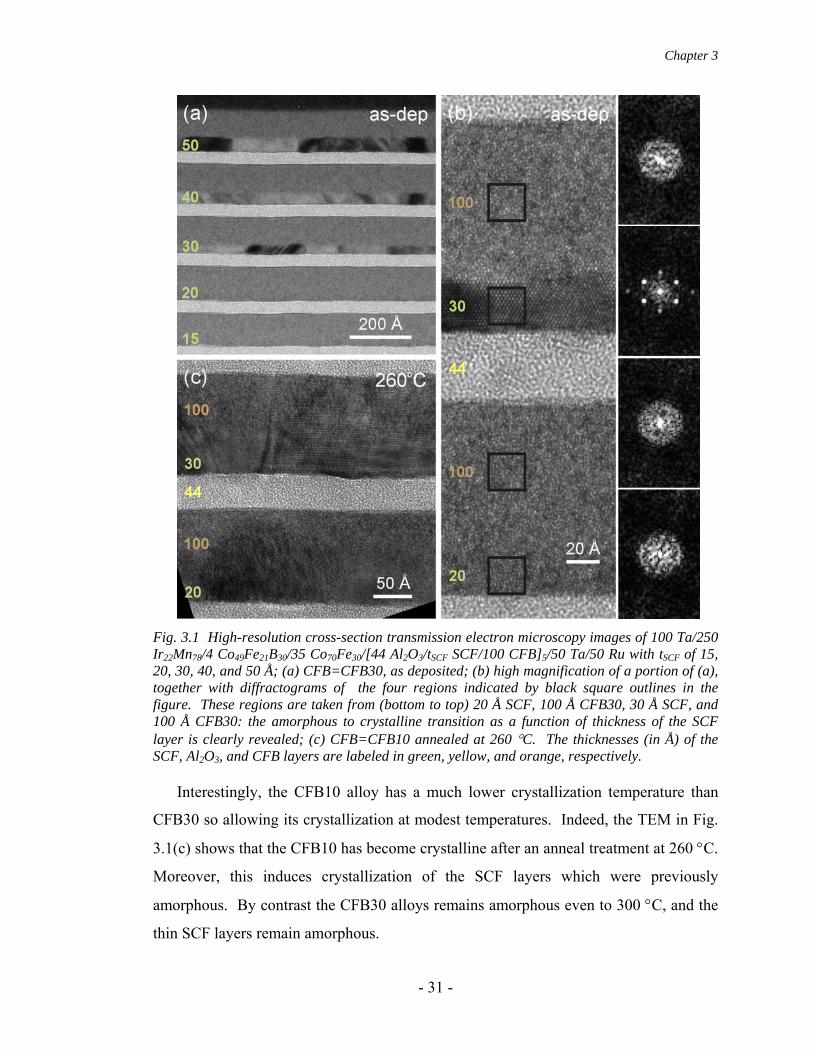
Chapter 3
Fig. 3.1 High-resolution cross-section transmission electron microscopy images of 100 Ta/250 Ir22Mn78/4 Co49Fe21B30/35 Co70Fe30/[44 Al2O3/tSCF SCF/100 CFB]5/50 Ta/50 Ru with tSCF of 15, 20, 30, 40, and 50 Å; (a) CFB=CFB30, as deposited; (b) high magnification of a portion of (a), together with diffractograms of the four regions indicated by black square outlines in the figure. These regions are taken from (bottom to top) 20 Å SCF, 100 Å CFB30, 30 Å SCF, and 100 Å CFB30: the amorphous to crystalline transition as a function of thickness of the SCF layer is clearly revealed; (c) CFB=CFB10 annealed at 260 °C. The thicknesses (in Å) of the SCF, Al2O3, and CFB layers are labeled in green, yellow, and orange, respectively.
Interestingly, the CFB10 alloy has a much lower crystallization temperature than
CFB30 so allowing its crystallization at modest temperatures. Indeed, the TEM in Fig.
3.1(c) shows that the CFB10 has become crystalline after an anneal treatment at 260 °C.
Moreover, this induces crystallization of the SCF layers which were previously
amorphous. By contrast the CFB30 alloys remains amorphous even to 300 °C, and the
thin SCF layers remain amorphous.
- 31 -
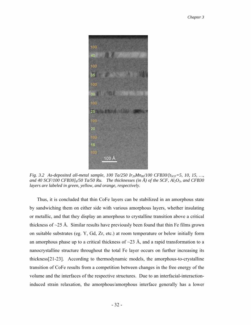
Chapter 3
Fig. 3.2 As-deposited all-metal sample, 100 Ta/250 Ir20Mn80/100 CFB30/[tSCF=5, 10, 15, …, and 40 SCF/100 CFB30]8/50 Ta/50 Ru. The thicknesses (in Å) of the SCF, Al2O3, and CFB30 layers are labeled in green, yellow, and orange, respectively.
Thus, it is concluded that thin CoFe layers can be stabilized in an amorphous state
by sandwiching them on either side with various amorphous layers, whether insulating
or metallic, and that they display an amorphous to crystalline transition above a critical
thickness of ~25 Å. Similar results have previously been found that thin Fe films grown
on suitable substrates (eg. Y, Gd, Zr, etc.) at room temperature or below initially form
an amorphous phase up to a critical thickness of ~23 Å, and a rapid transformation to a
nanocrystalline structure throughout the total Fe layer occurs on further increasing its
thickness[21-23]. According to thermodynamic models, the amorphous-to-crystalline
transition of CoFe results from a competition between changes in the free energy of the
volume and the interfaces of the respective structures. Due to an interfacial-interaction-
induced strain relaxation, the amorphous/amorphous interface generally has a lower
- 32 -
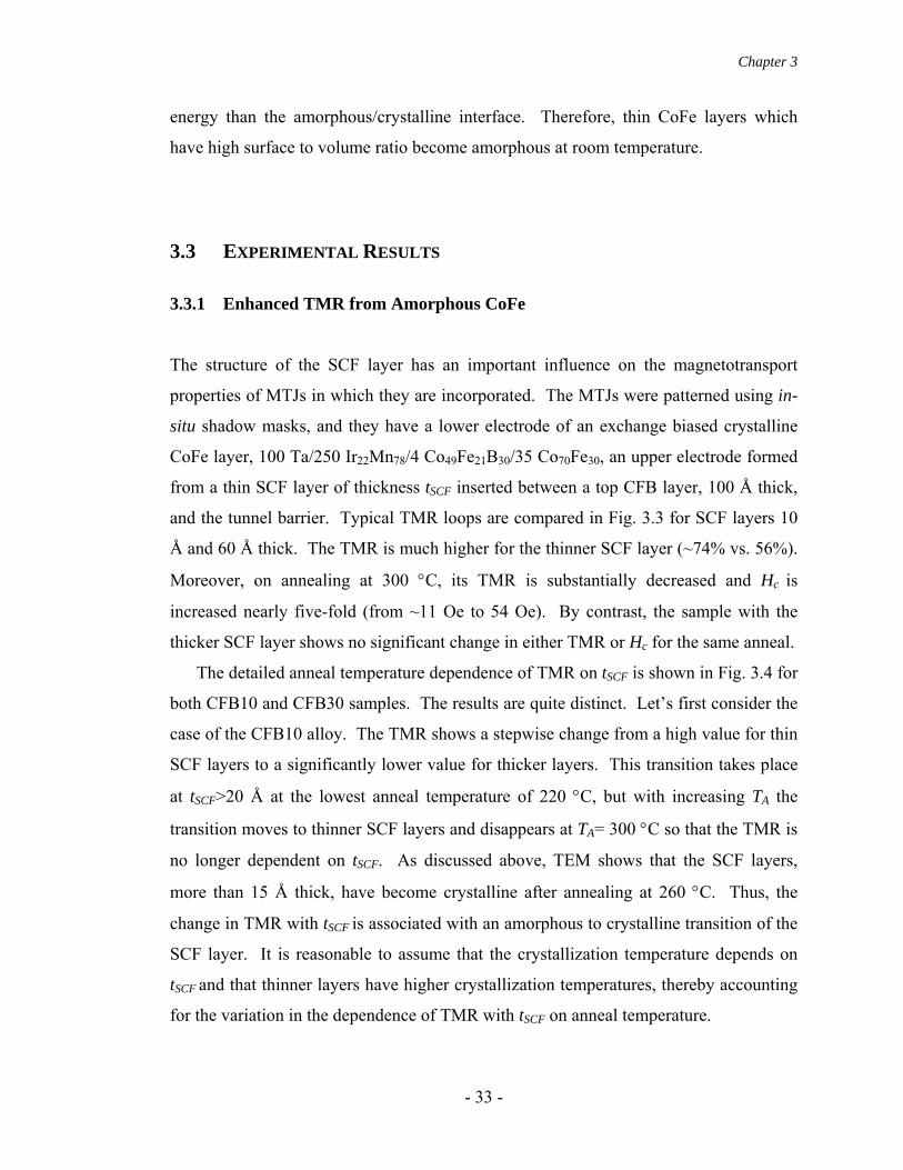
Chapter 3
energy than the amorphous/crystalline interface. Therefore, thin CoFe layers which
have high surface to volume ratio become amorphous at room temperature.
3.3 EXPERIMENTAL RESULTS
3.3.1 Enhanced TMR from Amorphous CoFe
The structure of the SCF layer has an important influence on the magnetotransport
properties of MTJs in which they are incorporated. The MTJs were patterned using in-
situ shadow masks, and they have a lower electrode of an exchange biased crystalline
CoFe layer, 100 Ta/250 Ir22Mn78/4 Co49Fe21BB30/35 Co70Fe30, an upper electrode formed
from a thin SCF layer of thickness tSCF inserted between a top CFB layer, 100 Å thick,
and the tunnel barrier. Typical TMR loops are compared in Fig. 3.3 for SCF layers 10
Å and 60 Å thick. The TMR is much higher for the thinner SCF layer (~74% vs. 56%).
Moreover, on annealing at 300 °C, its TMR is substantially decreased and Hc is
increased nearly five-fold (from ~11 Oe to 54 Oe). By contrast, the sample with the
thicker SCF layer shows no significant change in either TMR or Hc for the same anneal.
The detailed anneal temperature dependence of TMR on tSCF is shown in Fig. 3.4 for
both CFB10 and CFB30 samples. The results are quite distinct. Let’s first consider the
case of the CFB10 alloy. The TMR shows a stepwise change from a high value for thin
SCF layers to a significantly lower value for thicker layers. This transition takes place
at tSCF>20 Å at the lowest anneal temperature of 220 °C, but with increasing TA the
transition moves to thinner SCF layers and disappears at TA= 300 °C so that the TMR is
no longer dependent on tSCF. As discussed above, TEM shows that the SCF layers,
more than 15 Å thick, have become crystalline after annealing at 260 °C. Thus, the
change in TMR with tSCF is associated with an amorphous to crystalline transition of the
SCF layer. It is reasonable to assume that the crystallization temperature depends on
tSCF and that thinner layers have higher crystallization temperatures, thereby accounting
for the variation in the dependence of TMR with tSCF on anneal temperature.
- 33 -
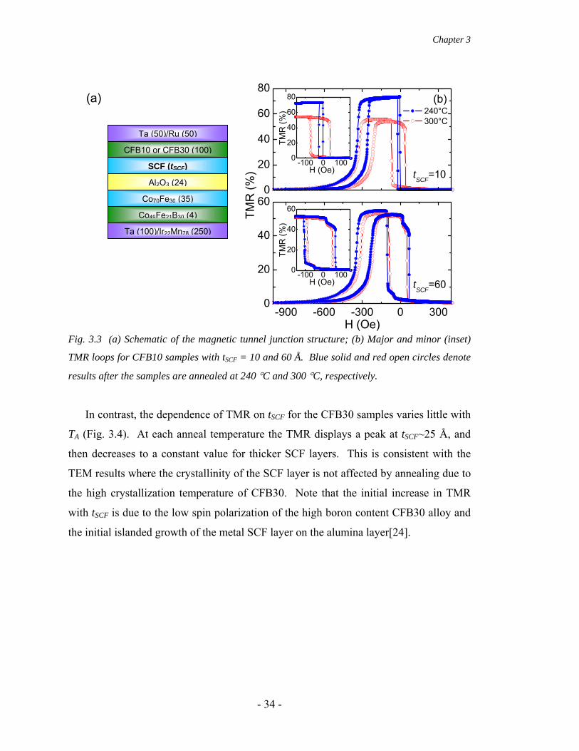
Chapter 3
-900 -600 -300 0 3000
20
40
60
-100 0 1000
20
40
60
-100 0 1000
20
40
60
80
tSCF=60
H (Oe)
0
20
40
60
80
240°C 300°C
(b)
tSCF=10
TMR
(%)
TMR
(%)
H (Oe)TM
R (%
)
H (Oe)
Ta (100)/Ir22Mn78 (250)
Co70Fe30 (35) Co49Fe21B30 (4)
Al2O3 (24)
CFB10 or CFB30 (100) SCF (tSCF)
Ta (50)/Ru (50)
(a)
Fig. 3.3 (a) Schematic of the magnetic tunnel junction structure; (b) Major and minor (inset)
TMR loops for CFB10 samples with tSCF = 10 and 60 Å. Blue solid and red open circles denote
results after the samples are annealed at 240 °C and 300 °C, respectively.
In contrast, the dependence of TMR on tSCF for the CFB30 samples varies little with
TA (Fig. 3.4). At each anneal temperature the TMR displays a peak at tSCF~25 Å, and
then decreases to a constant value for thicker SCF layers. This is consistent with the
TEM results where the crystallinity of the SCF layer is not affected by annealing due to
the high crystallization temperature of CFB30. Note that the initial increase in TMR
with tSCF is due to the low spin polarization of the high boron content CFB30 alloy and
the initial islanded growth of the metal SCF layer on the alumina layer[24].
- 34 -
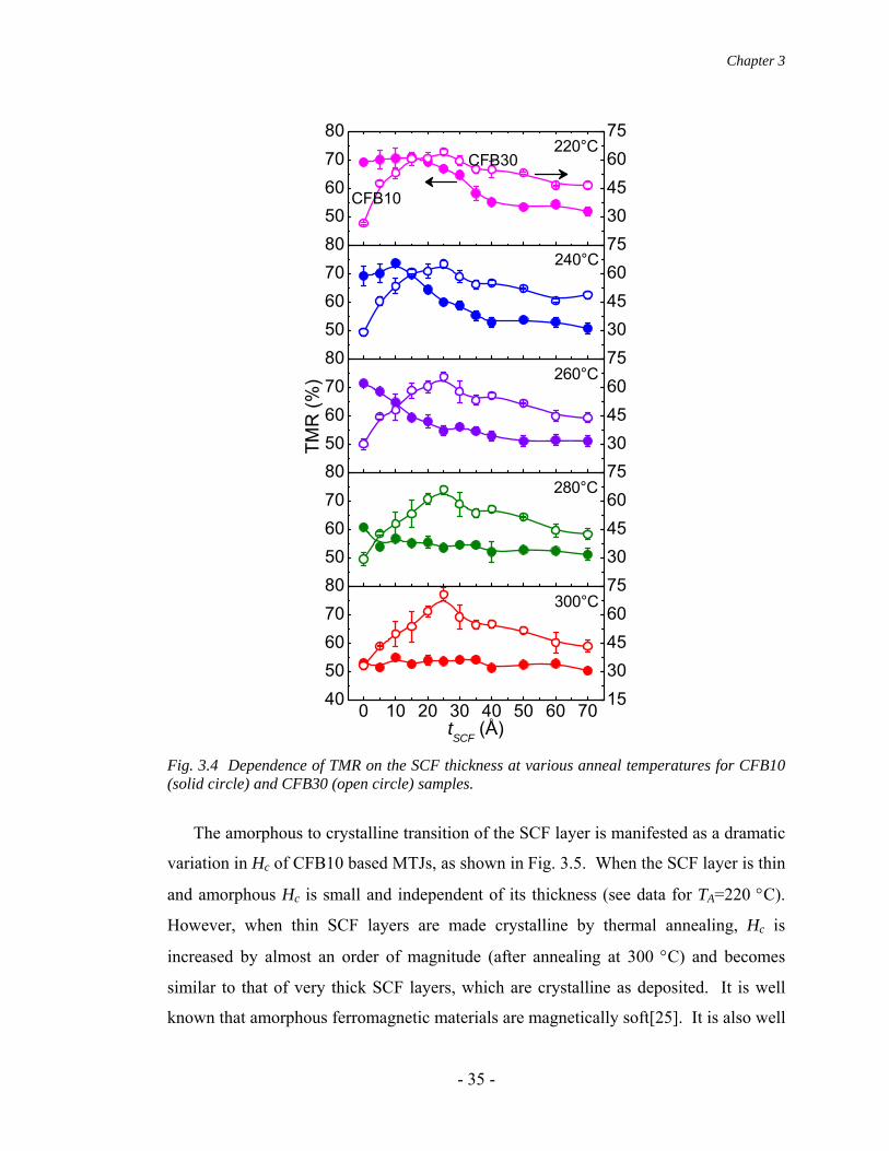
Chapter 3
50607080
220°C
50607080
240°C
50607080
TMR
(%) 260°C
50607080
280°C
0 10 20 30 40 50 60 704050607080
tSCF
(Å)
300°C
30456075
30456075
30456075
30456075
1530456075
CFB10
CFB30
Fig. 3.4 Dependence of TMR on the SCF thickness at various anneal temperatures for CFB10 (solid circle) and CFB30 (open circle) samples.
The amorphous to crystalline transition of the SCF layer is manifested as a dramatic
variation in Hc of CFB10 based MTJs, as shown in Fig. 3.5. When the SCF layer is thin
and amorphous Hc is small and independent of its thickness (see data for TA=220 °C).
However, when thin SCF layers are made crystalline by thermal annealing, Hc is
increased by almost an order of magnitude (after annealing at 300 °C) and becomes
similar to that of very thick SCF layers, which are crystalline as deposited. It is well
known that amorphous ferromagnetic materials are magnetically soft[25]. It is also well
- 35 -
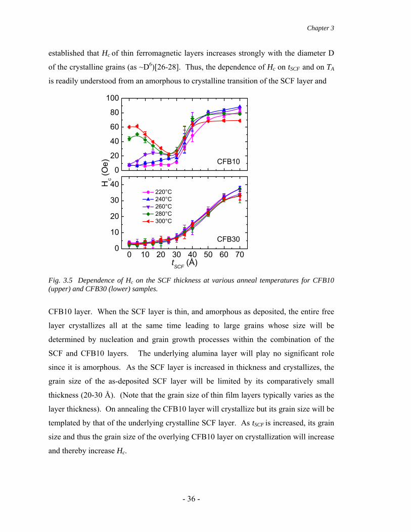
Chapter 3
established that Hc of thin ferromagnetic layers increases strongly with the diameter D
of the crystalline grains (as ~D6)[26-28]. Thus, the dependence of Hc on tSCF and on TA
is readily understood from an amorphous to crystalline transition of the SCF layer and
0 10 20 30 40 50 60 700
10
20
30
40
Hc (O
e)
tSCF (Å)
CFB30
0
20
40
60
80
100
220°C 240°C 260°C 280°C 300°C
CFB10
Fig. 3.5 Dependence of Hc on the SCF thickness at various anneal temperatures for CFB10 (upper) and CFB30 (lower) samples.
CFB10 layer. When the SCF layer is thin, and amorphous as deposited, the entire free
layer crystallizes all at the same time leading to large grains whose size will be
determined by nucleation and grain growth processes within the combination of the
SCF and CFB10 layers. The underlying alumina layer will play no significant role
since it is amorphous. As the SCF layer is increased in thickness and crystallizes, the
grain size of the as-deposited SCF layer will be limited by its comparatively small
thickness (20-30 Å). (Note that the grain size of thin film layers typically varies as the
layer thickness). On annealing the CFB10 layer will crystallize but its grain size will be
templated by that of the underlying crystalline SCF layer. As tSCF is increased, its grain
size and thus the grain size of the overlying CFB10 layer on crystallization will increase
and thereby increase Hc.
- 36 -
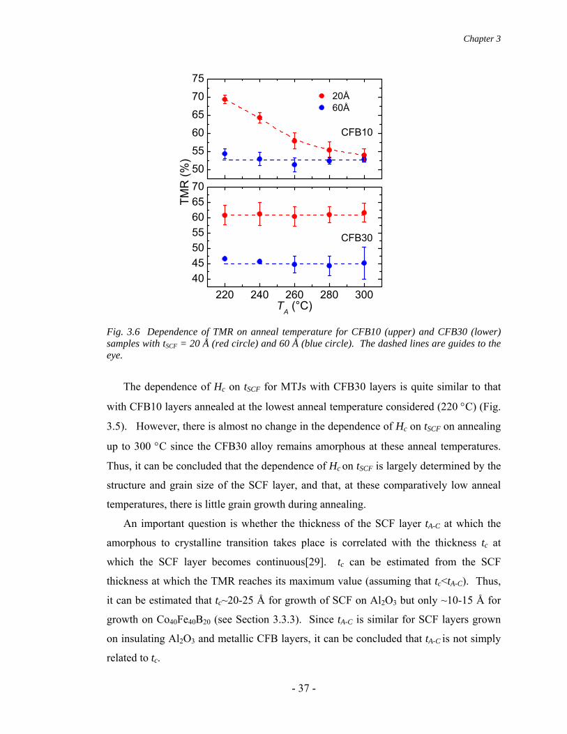
Chapter 3
220 240 260 280 30040455055606570
20Å60Å
TM
R (%
)
TA (°C)
CFB30
505560657075
CFB10
Fig. 3.6 Dependence of TMR on anneal temperature for CFB10 (upper) and CFB30 (lower) samples with tSCF = 20 Å (red circle) and 60 Å (blue circle). The dashed lines are guides to the eye.
The dependence of Hc on tSCF for MTJs with CFB30 layers is quite similar to that
with CFB10 layers annealed at the lowest anneal temperature considered (220 °C) (Fig.
3.5). However, there is almost no change in the dependence of Hc on tSCF on annealing
up to 300 °C since the CFB30 alloy remains amorphous at these anneal temperatures.
Thus, it can be concluded that the dependence of Hc on tSCF is largely determined by the
structure and grain size of the SCF layer, and that, at these comparatively low anneal
temperatures, there is little grain growth during annealing.
An important question is whether the thickness of the SCF layer tA-C at which the
amorphous to crystalline transition takes place is correlated with the thickness tc at
which the SCF layer becomes continuous[29]. tc can be estimated from the SCF
thickness at which the TMR reaches its maximum value (assuming that tc<tA-C). Thus,
it can be estimated that tc~20-25 Å for growth of SCF on Al2O3 but only ~10-15 Å for
growth on Co40Fe40BB20 (see Section 3.3.3). Since tA-C is similar for SCF layers grown
on insulating Al2O3 and metallic CFB layers, it can be concluded that tA-C is not simply
related to tc.
- 37 -
Chapter 3
The dependence of TMR on TA is summarized in Fig. 3.6 for free layers with
representative thicknesses of 20 and 60 Å thick SCF layers for the CFB10 and CFB30
alloys, respectively. For both CFB alloys the TMR is much higher for the 20 Å
amorphous as compared to the 60 Å crystalline SCF layer. Only for the thinner CFB10
alloy is any significant variation in TMR with TA observed. In this case, the TMR
decreases on annealing to the value found for thick SCF layers, which are crystalline as
deposited.
3.3.2 Increased TSP from Amorphous CoFe
It has been discussed that when amorphous SCF layers are integrated into MTJs with
amorphous alumina tunnel barriers, significantly higher TMR is observed compared to
when these layers are crystalline. In this section, tunneling spin polarization (TSP) will
be directly compared for both amorphous and crystalline CoFe alloys using
superconducting tunneling spectroscopy (STS). It is well established that the
magnetoresistance effect in MTJs derives from spin dependent tunneling, and is largely
determined by TSP. The magnitude of TMR can be formulated in terms of the TSP for
the two corresponding ferromagnetic (FM) electrodes, P1 and P2, as
[30]. The TSP can be obtained by measuring the STS from
superconductor/insulator/FM structures[31,32]. Indeed, it is found that the TSP is
significantly enhanced for amorphous CoFe compared to its crystalline counterpart,
consistent with the previous measurements of TMR.
(1 2 1 22 / 1TMR PP PP= − )
Two sets of STS samples were deposited with the basic structure: thermally
oxidized Si substrate/45 Al95Si5/32 Al2O3/tSCF SCF /100 CFB10, or CFB30/50 Ta/50
Ru. The thickness tSCF of the SCF layer varies from 0 to 70 Å. The superconducting
layer was formed from 45-Å-thick Al95Si5, where a small amount of Si is added to
increase the Al superconducting transition temperature[31]. The STS measurements
were conducted at ~0.250 K in a magnetic field of 2 T applied in the film plane for as-
deposited samples, and after annealing the samples at a series of temperatures from 220
°C to 300 °C. The annealing was carried out in vacuum (~5×10⁻⁸ Torr) in a 1 T
- 38 -


![[27] Circular Dichroism and Optical Rotatory …ctrstbio.org.uic.edu/manuals/adler.pdf678 CONFORMATION: OPTICAL SPECTROSCOPY [27] The Phenomena of CD and ORD A beam of linearly polarized](https://img.pdfslide.net/doc/110x75/5af35bc37f8b9a154c8ccc60/27-circular-dichroism-and-optical-rotatory-conformation-optical-spectroscopy.jpg)

![arXiv:1808.03957v1 [cond-mat.mes-hall] 12 Aug 2018 · 2018. 8. 14. · recent developments in spintronics with the novel material, the spin-polarized transport in graphene-based junctions](https://img.pdfslide.net/doc/110x75/612db7bc1ecc515869425cfa/arxiv180803957v1-cond-matmes-hall-12-aug-2018-2018-8-14-recent-developments.jpg)