Embed Size (px)
Citation preview

ST Silicon Carbide Productsand Industrial Application Guide
Karman Wu - Technical Marketing
Devin Xu - Power Discrete Application Engineer
Yolanda Zhang - Technical Marketing

1 About SiC material
2 ST SiC market overview
3 ST SiC diodes and feature
4 ST SiC MOSFETs
5 SiC MOSFET – switching and driving
6 New SiC related evalboards
7 ST support tools
Agenda
2

About SiC material
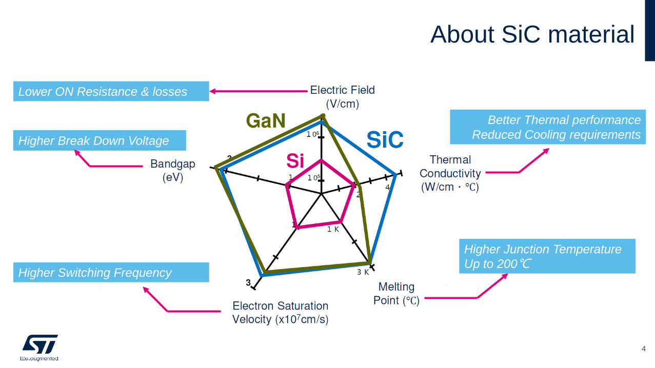
About SiC material
Higher Break Down Voltage
Lower ON Resistance & losses
Higher Switching Frequency
Higher Junction Temperature
Up to 200
Better Thermal performance
Reduced Cooling requirements
4

Key figures for SiC vs. Silicon
x3
Sic Vs. Si
Resistivity
1/300
(At same applied Voltage)
Thermal
Conductivity
Higher Thermal
Insensivity
Switching Losses
-80%IGBT
vs.
SiC Vs. Silicon
Material PropertiesSiC Vs. IGBT Performance
Component
Volume Dimension
-85%Component
Weight
-80%
SiC Module
mainly due to lower
Resistance
5
Source: Goldman Sachs

ST SiC market overview

Silicon Carbide market outlook
7
Source: Omdia/IHS – SiC & GaN World 2020 Forecast & output Tables – mid case
(June 2020)
[$M]
SiC power semiconductors by macro product family
28%
16%
13%
Automotive
Industrial**
Others*
CAGR Y’19-’29
2019 2029
Others Application
Traction
Aerospace and Military
PV inverters
Industrial Motor Drives
EV charging stations
Commercial vehicles
HEV/EV
UPS
Power supplies
654.6
3,732
CAGR(19-29): 19%CAGR(19-29)
14.5%
19%
11%
11%
134%
5.3%
33%
27.5%
17%
16.5%
*Military and aerospace, traction, Other applications
**renewable energies applications included
SiC power semiconductors by application
2.4B$ on 2025 (GAGR 19-25: 24.0%)
2019 2029
Full Sic Modules
Hybrid modules
JFETs
MOSFETs
Diodes
[$ M]
CAGR(19-29)
33%
8.2%
21.67%
654.6
3,732
18.5%
16.3%

ST mastering all Silicon Carbide manufacturing steps
8
June 1996:
Collaboration with
Physics Dept.
May 2004:
Schottky Diode
Demonstrator (ST)
October 2007:
1st Gen DIODE
Start Production
March 2009:
Power MOSFET
3" Demonstrator
February 2003: ETC
Epitaxial reactor
prototype installed in ST
April 1998:
1st contract on SiC
with CNR-IMETEM
May 2002: Schottky
Diode Demonstrator
(CNR line)
2003: 2" ST line 2006: 3" ST line 2011: 4" ST line 2016: 6" ST line
May 2012:
2nd Gen DIODE
Start Production
1996
September 2014:
1st Gen MOSFET
Start Production
June 2014:
3rd Gen DIODE
Start Production
ST Major Milestones
2016
Catania: Power Electronics Competence Center
Ecosystem made of Academic Research Centers and ST as a semiconductor
leader, created a true “incubator”
More Than 70 Patents on SiC
Everything started from 1’’ wafer
ST Commitment on SiC
Leveraging on CNR Facilities at early stage
> 30 Years Experience in Power Semiconductor
Pioneering WBG materials, with longer than 20 years commitment in R&D
June 2017
2nd Gen MOSFET
Start Production

STPOWER Silicon Carbide MOSFETs
9
• Vertical integration through Norstel AB acquisition
• Extended supply chain capability through multi-year supply agreement
• Continue to invest to expand ST capacity
ST committed to develop its SiC Supply Chain
• ST broad range of SiC solutions: Discrete, Bare
Dice, Module
• ST proven very high reliability
• ST continue capacity expansion to support
market acceleration
• ST invests on advanced package technologies
Best-in-class SiC Technology
Front-end Evolution
x2 shrink
1st Gen
Gen 2nd Gen
Gen In Production
x4 shrink
Planar
Planar 3rd Gen Next
Gen
Continuous Shrinkage[Ron x cm2]
Planar
Under qualification
(Q4/’20) In Development

KEY APPLICATIONS
• Traction Inverter
• OBC
• DC/DC Converter
• Environment: WW CO2 emission reduction program
• Car electrification huge growth trend
• Smaller and lighter power unit form factor
• Better Inverter efficiency SiC MOSFET vs. IGBT (extra
mileage / lower battery cost)
GROWTH DRIVERSCar Electrification
• Solar Inverter
• Energy Storage
• Power Supply
• Charging Station
• Welding
• Drives
KEY APPLICATIONS
• Better efficiency
• Smaller form factor
• Lower TCO vs. silicon technologies
GROWTH DRIVERS High End Industrial
STPOWER SiC MOSFET focused market
10
ST SiC diodes and feature

650V SiC Diodes product portfolio
IFSM/IF(AV)
(25°C / 10ms)
VF
(Max value at I0 / 25°C)1.65V1.45V 1.55V 1.75V
2
4
6
8
10
High Surge CapabilitySTPSCxxH065x
High EfficiencySTPSCxx065x
1.35V
200mV Lower VF
12

650V SiC Diodes product portfoliolatest releases
TO247 TO-247 LL TO-220 TO-220I D2PAK D²PAK HV DPAK PowerFLAT 8x8 HV
650V
Low VF
STPSC12065
STPSC10065
STPSC8065
STPSC20065
STPSC20065C
STPSC40065C
High Surge Capability
STPSC16H065A
STPSC16H065C
STPSC12H065
STPSC12H065C
STPSC10H065
STPSC8H065
STPSC8H065C
STPSC6H065
STPSC4H065
STPSC20H065C
NCNCAA
K
D²PAK HV
PowerFLAT8x8
TO-247 LL
I FAV(A) 16A
12A
10A
8A
6A
4A
20A
40A
2A STPSC2H065
SiC Diodes in new packages
13

New PowerFLAT 8x8 package
More Guard Band
to grid disturbances
D2PAK DPAK PowerFLAT 8x8
&
The ultimate Watts
improvement
Every mV grants efficiency
toward 97%, 98%, 99%
0.00
0.50
1.00
1.50
2.00
2.50
3.00
VF I0 25°C VF I0 150°C
VF
Max (
V)
STPSCxH065
STPSCxH065DLF
… inside a less-than-1-mm thick package
14

An improved Creepage Design
HIGH CREEPAGE
Greater Package and
Footprint Creepage
than DPAK1.80mm
EA
SY
CO
MP
LIA
NC
E
TO
IE
C-6
06
64
-1*
*Basic Safety Standard Insulation
New PowerFLAT 8x8 package
1.36mm
2.68mm
DP
AK
Pow
erF
LA
T™
8x8
HV
2.60mm
2.75mm
15

• Benchmark on VF
STPOWER SiC 1200V Diode
1.5V 1.70V 1.8V 1.9V
IFSM / IF(AV)
(25°C / 10ms)
4
6
8
VF max (Io / 25°C)
STPSCxxH12
10
1.6V
Other 1200V
SiC diodes
Current
best VF
solution
Other 1200V
SiC diodes
Up to 300mV better VF
ST new SiC 1200V diode: the market reference on VF16

Reverse recovery -What is the practical difference?Let’s look at an example…

650V SiC Diode performances vs. Si Diode technology
Power losses due to D1 only
=
+0.2% = +0.2%
= +0.17%
= +0.06%
AC
Interleaved PFC
D1
D2
T1
T2
With SiC, we get :
• Best switching performance (fast and soft)
• Best efficiency in hard-switching applications thanks to best turn-off performance
Interleaved PFC 3.3kW: Power losses sharing
18

• Drain current driven by 𝑉𝐺𝑆
• MOSFET channel starts
conducting at full 𝑉𝐷𝑆 voltage
Hard switchingExample: Boost in CCM, #1
Lo
ad
C1
L
C2
𝑣𝐺𝑆
𝑣𝐷𝑆
Dri
ve
r
𝑖𝑆
𝑉𝐼𝑁RG
𝑖𝐿
D1
19

• Drain current driven by 𝑉𝐺𝑆
• MOSFET channel starts
conducting at full 𝑉𝐷𝑆 voltage
Hard switchingExample: Boost in CCM, #2
Lo
ad
C1
L
C2
𝑣𝐺𝑆
𝑣𝐷𝑆
Dri
ve
r
𝑖𝑆
𝑉𝐼𝑁
𝑖𝐿
RG
D1
20

• Drain current driven by 𝑉𝐺𝑆
• MOSFET channel starts
conducting at full 𝑉𝐷𝑆 voltage
Hard switchingExample: Boost in CCM, #3
Lo
ad
C1
L
C2
𝑣𝐺𝑆
𝑣𝐷𝑆
Dri
ve
r
𝑖𝑆
𝑉𝐼𝑁
𝑖𝐿
RG
𝑖𝑅𝑅
D1
21

• Drain current driven by 𝑉𝐺𝑆
• MOSFET channel starts
conducting at full 𝑉𝐷𝑆 voltage
Hard switchingExample: Boost in CCM, #4
Lo
ad
C1
L
C2
𝑣𝐺𝑆
𝑣𝐷𝑆
Dri
ve
r
𝑖𝑆
𝑉𝐼𝑁
𝑖𝐿
RG
𝑖𝑅𝑅
D1
22

• Drain current driven by 𝑉𝐺𝑆
• MOSFET channel starts
conducting at full 𝑉𝐷𝑆 voltage
Hard switchingExample: Boost in CCM, #5
Lo
ad
C1
L
C2
𝑣𝐺𝑆
𝑣𝐷𝑆
Dri
ve
r
𝑖𝑆
𝑉𝐼𝑁RG
𝑖𝐿
D1
23

• Drain current driven by 𝑉𝐺𝑆
• MOSFET channel starts
conducting at full 𝑉𝐷𝑆 voltage
Hard switchingExample: Boost in CCM, #6
Reverse recovery of
the boost diode D1
Area ~ 𝑄𝑅𝑅
• 𝑄𝑅𝑅 dissipated in the MOSFET
24
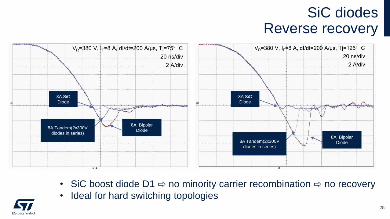
SiC diodesReverse recovery
25
• SiC boost diode D1 no minority carrier recombination no recovery
• Ideal for hard switching topologies
8A SiC
Diode
8A Tandem(2x300V
diodes in series)
8A Bipolar
Diode
8A SiC
Diode
8A Tandem(2x300V
diodes in series)
8A Bipolar
Diode

SiC MOSFET Products

STPOWER SiC MOSFET series positioning
27
650V 1200V 1700V
G2 G1 G2 G1
Breakdown Voltage
Series
RDS(on) mΩ
Focus Applications
18-55 52-520 22-75
Renewable energy
Power Supply
OBC, DC-DC
Power Conversion
Industrial drives
High Voltage
Power Supply
DC-DC
Street Lighting
Charging stations
OBC, DC-DC, Traction
Photovoltaic
HVAC
ID Current
45-120A 12-65A 40-100A 6-25A
65-700
AG Qualification available

Part Number VDS [V]RDS(on) Typ@ 25 ºC [Ω]
Id [A]
Package
HiP247 HiP247-LL HiP247-4LL H2PAK-2L H2PAK-7L
Tj max= 200°C
1200 Gen1 (Vgs=18V) series
SCT50N120
1200
0.052 65
X
SCTWA50N120 X
SCTWA50N120-4 X
SCTH50N120-7 X
SCT30N120
0.080 40X
SCTWA30N120 X
SCT30N120H X
SCT20N120
0.169 20
X
SCTWA20N120 X
SCT20N120H X
SCT20N120AG X
SCT10N120
0.520 12
X
SCTWA10N120 X
SCT10N120H X
SCT10N120AG X
SiC MOSFET in Mass Production:1200V Gen1 (1/3)
The Best Rdson vs. Tj behavior Option
Automotive Grade
28
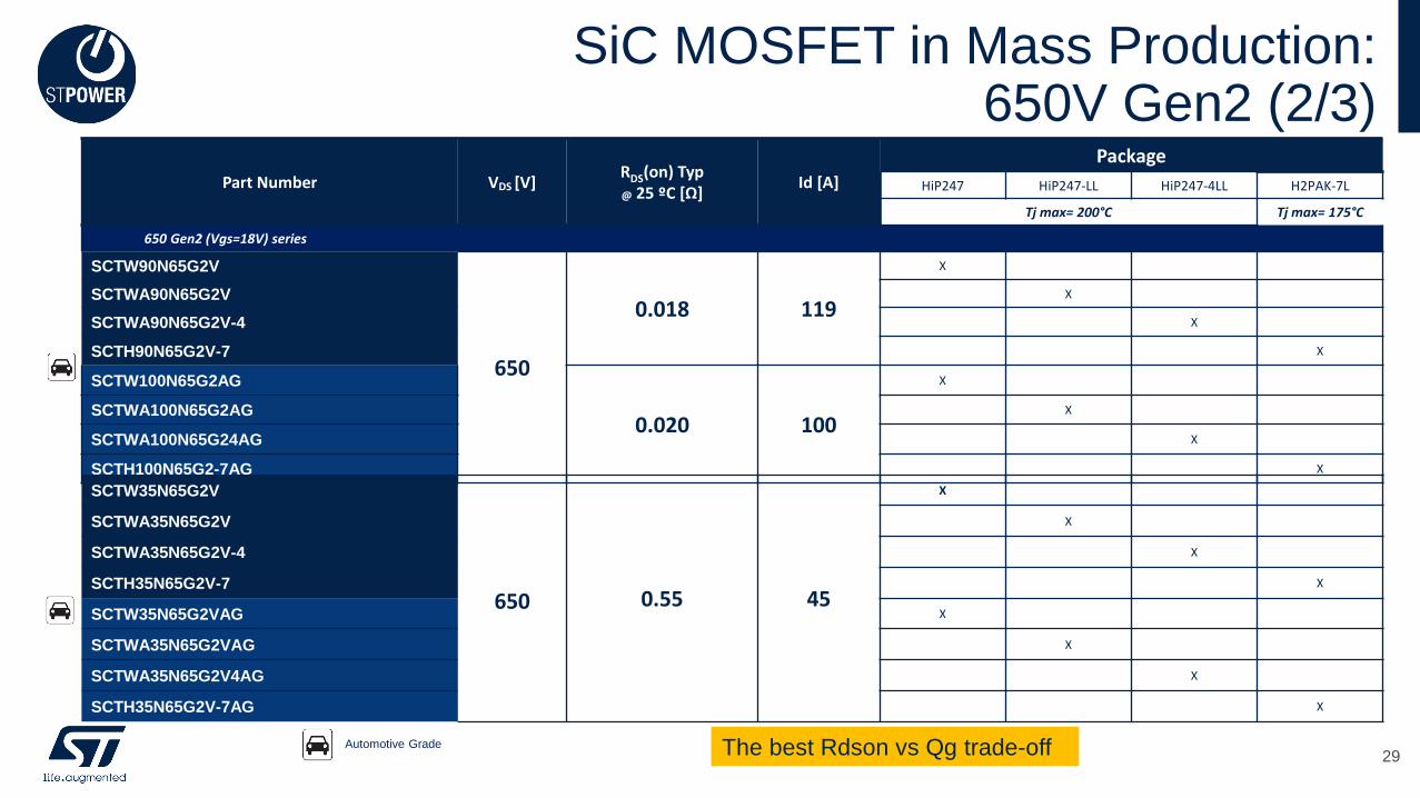
SiC MOSFET in Mass Production: 650V Gen2 (2/3)
Part Number VDS [V]RDS(on) Typ@ 25 ºC [Ω]
Id [A]
Package
HiP247 HiP247-LL HiP247-4LL H2PAK-7L
Tj max= 200°C Tj max= 175°C
650 Gen2 (Vgs=18V) series
SCTW90N65G2V
650
0.018 119
X
SCTWA90N65G2V X
SCTWA90N65G2V-4 X
SCTH90N65G2V-7 X
SCTW100N65G2AG
0.020 100
X
SCTWA100N65G2AG X
SCTWA100N65G24AG X
SCTH100N65G2-7AG X
SCTW35N65G2V
650 0.55 45
X
SCTWA35N65G2V X
SCTWA35N65G2V-4 X
SCTH35N65G2V-7 X
SCTW35N65G2VAG X
SCTWA35N65G2VAG X
SCTWA35N65G2V4AG X
SCTH35N65G2V-7AG X
Automotive Grade The best Rdson vs Qg trade-off 29
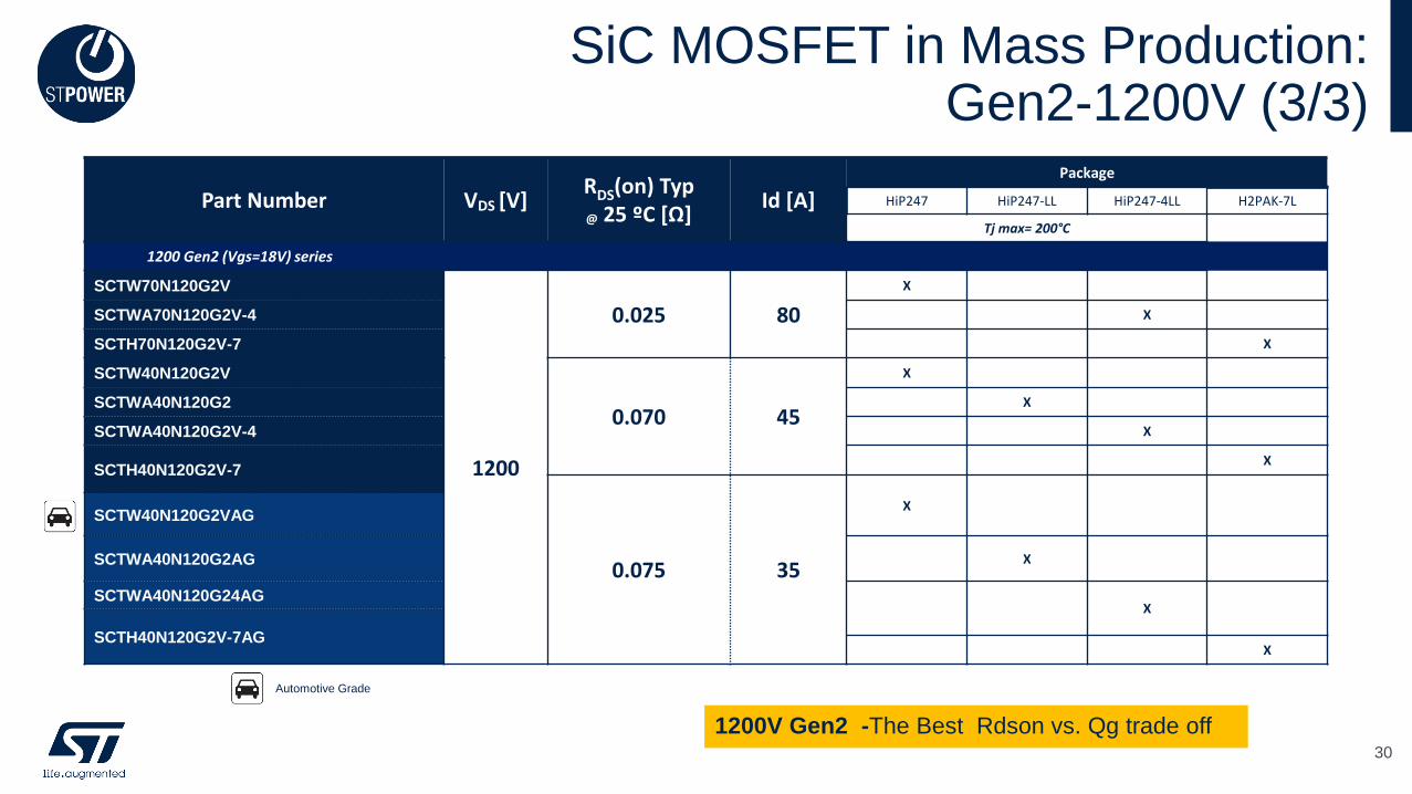
SiC MOSFET in Mass Production: Gen2-1200V (3/3)
1200V Gen2 -The Best Rdson vs. Qg trade off
Automotive Grade
Part Number VDS [V]RDS(on) Typ
@ 25 ºC [Ω]Id [A]
Package
HiP247 HiP247-LL HiP247-4LL H2PAK-7L
Tj max= 200°C
1200 Gen2 (Vgs=18V) series
SCTW70N120G2V
1200
0.025 80
X
SCTWA70N120G2V-4 X
SCTH70N120G2V-7 X
SCTW40N120G2V
0.070 45
X
SCTWA40N120G2 X
SCTWA40N120G2V-4 X
SCTH40N120G2V-7X
0.075 35
XSCTW40N120G2VAG
SCTWA40N120G2AG X
SCTWA40N120G24AGX
SCTH40N120G2V-7AGX
30

SiC MOSFET Product Plan1700V devices being introduced in mass production
Part Number VDS [V]RDS(on) Typ
@ 25 ºC [Ω]Id [A]
PackageHiP247 HiP247-LL HiP247-4LL H2PAK-2L H2PAK-7L
Tj max= 200°C Tj max= 175°C
1200 Gen2 (Vgs=18V) series
SCT1000N170
1700V
1 6
X
SCT1000N170AG X
SCTWA1000N170 X
SCT20N170
0.064 25
X
SCT20N170AG X
SCTWA20N170 X
1700V SiC MOSFET’s – The First Very High Voltage
devices Automotive & Industrial Qualified
Automotive grade
31

SiC MOSFET: advanced packaging technologiesPackage offer - Discrete – Bare Dice – Advanced packages
• Increase Power Density
• Reduce parasitic effects
• Target higher efficiency
Key advantages to…
Bare Dice Strategic offer for Key Players
SiC Forthcoming Packages
ACEPACK SMIT
HiP247-4L HiP247 HiP247-LL H2PAK
Available Packages
STPAK
PowerFLAT
32HU3PAK
Rated at
200°C!!!
ACEPACK
DRIVE
ACEPACK 1 & 2
TO220FP DPAK

Switching performance measurement

Half-Bridge testing platformBuck / Boost
Deliv
era
ble
s
• SiC MOSFET switching behavior, in
combination with Switch/Diode
• Dynamic losses of power semiconductors
• Reference design for STGAP2
• Reference design for DC/DC converter
STGAP2
DC-DC
Isolated
DC-DC
Isolated
STGAP2
LCIN
COUT
Q1
Q2
Control Unit
Power stage board
SiC Half-Bridge
Gate driver sub-board
Isolated DC/DC sub-board
Control unit
connector
Control board based
on STM32 MCU
Terminals for external inductor
34

Double pulse testPrinciple of operation #1
T0: Idle StageAlways turned off
*Device Under Test
Lo
ad
C1
L
C2
Input voltage
𝑖𝑆
𝑣𝐷𝑆
DUT*
HB
co
ntr
ol
𝑖𝐿
The Double-Pulse test is perfectly suited to measure the
switching energy of a DUT (Device Under Test)35

Double pulse testPrinciple of operation #2
𝑑𝑖
𝑑𝑡=
𝑉𝐿
𝐿 current increases with
a constant slope
Lo
ad
C1
L
C2
Input voltage
𝑖𝑆
𝑣𝐷𝑆
DUT*
HB
co
ntr
ol
𝑖𝐿
T1: Linear current Increase
T1 long enough to reach the
wished current level.
*Device Under Test
36

Double pulse testPrinciple of operation #3
T2 long enough to wait for switch-off transient, but
not too long to decrease inductor current too much.L
oad
C1
L
C2
Input voltage
𝑖𝑆
𝑣𝐷𝑆
DUT*
HB
co
ntr
ol
𝑖𝐿
T2: Free-Wheeling Phase
*Device Under Test
37

Double pulse testPrinciple of operation #4
T3 long enough to wait for
switch-on transient.L
oad
C1
L
C2
Input voltage
𝑖𝑆
𝑣𝐷𝑆
DUT*
HB
co
ntr
ol
𝑖𝐿
T3: 2nd Linear Increase Phase
*Device Under Test
38

Double pulse testPrinciple of operation #5
Sufficient load to dissipate energy from the
inductor before the next periodT4 long enough to demagnetize the
inductor.L
oad
C1
L
C2
Input voltage
𝑖𝑆
𝑣𝐷𝑆
DUT*
HB
co
ntr
ol
𝑖𝐿
T4: Reset Phase
*Device Under Test
39

Switching energy measurementTurn-on/off transient detail
𝑅𝐺 = 10 Ω, 𝐼𝑃𝐾 = 30 𝐴
𝑣𝐷𝑆
𝑖𝑆
𝑝
න 𝑝 𝑑𝑡
𝑣𝐺𝑆
Turn-on transient
𝑣𝐷𝑆
𝑖𝑆
𝑝
න 𝑝 𝑑𝑡
𝑣𝐺𝑆
Turn-off transient
The switching energy is calculated by integrating the product of 𝑣𝐷𝑆 and 𝑖𝑆 40
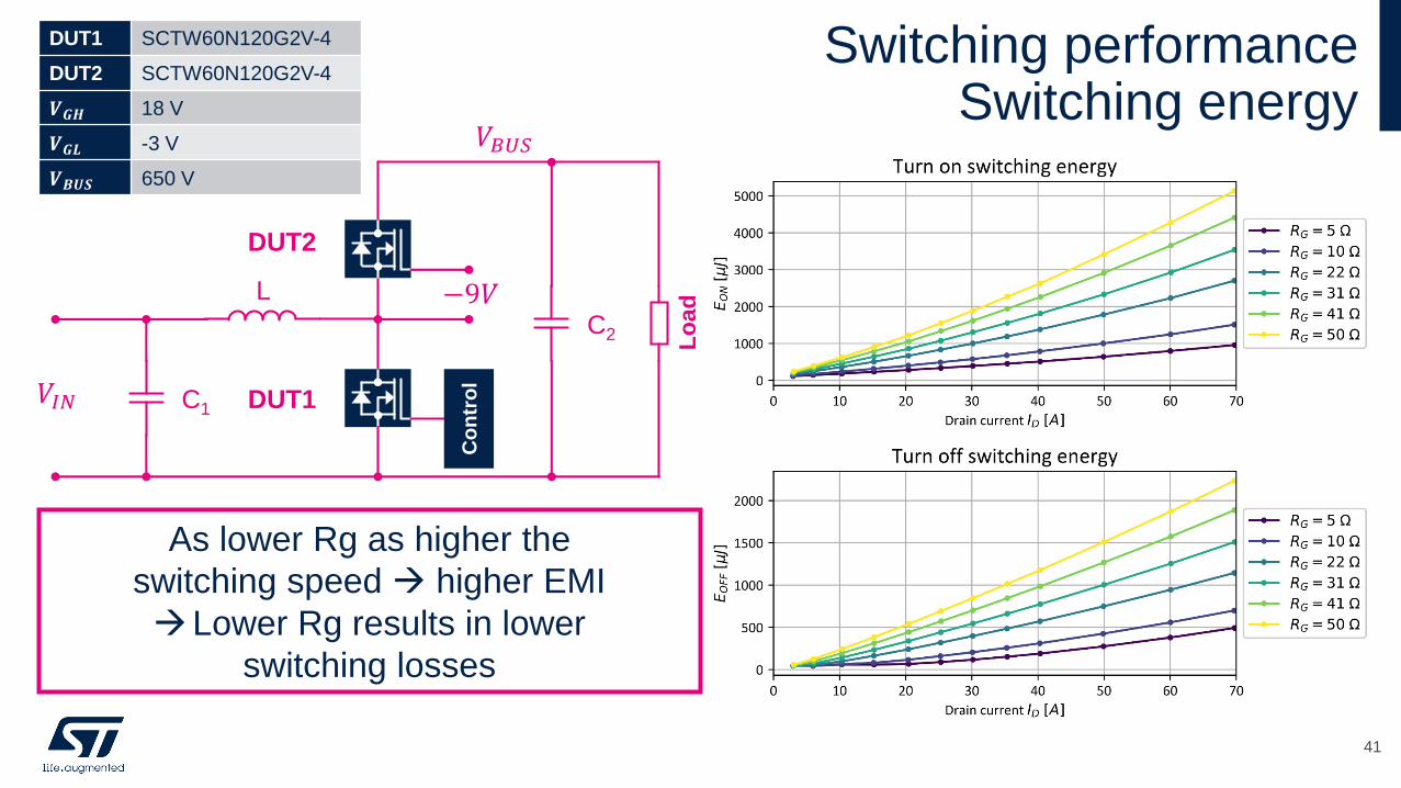
Switching performanceSwitching energy
Lo
ad
C1
L
C2
DUT1
Co
ntr
ol
DUT2
𝑉𝐵𝑈𝑆
𝑉𝐼𝑁
−9𝑉
DUT1 SCTW60N120G2V-4
DUT2 SCTW60N120G2V-4
𝑽𝑮𝑯 18 V
𝑽𝑮𝑳 -3 V
𝑽𝑩𝑼𝑺 650 V
As lower Rg as higher the
switching speed higher EMI
Lower Rg results in lower
switching losses
41

Switching performanceMaximum voltage slope
Lo
ad
C1
L
C2
DUT1
Co
ntr
ol
DUT2
𝑉𝐵𝑈𝑆
𝑉𝐼𝑁
−9𝑉
High 𝑑𝑣/𝑑𝑡 immunity of
gate driver is required
> 60 𝑉/𝑛𝑠
DUT1 SCTW60N120G2V-4
DUT2 SCTW60N120G2V-4
𝑽𝑮𝑯 18 V
𝑽𝑮𝑳 -3 V
𝑽𝑩𝑼𝑺 650 V
42

Standard vs. Kelvin source version
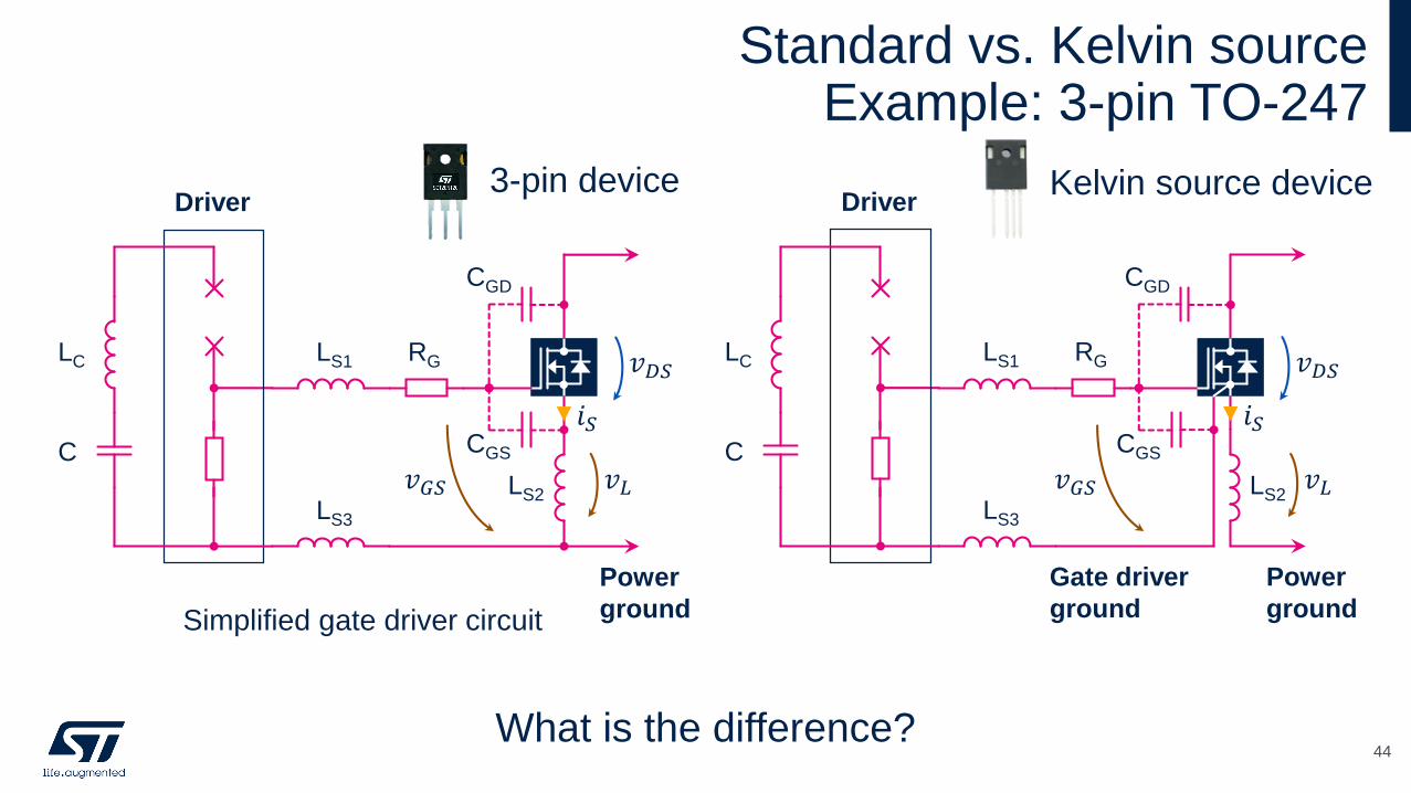
Standard vs. Kelvin source Example: 3-pin TO-247
Power
ground
Driver
C
LS1
LS2LS3
LC
CGS
𝑣𝐿
RG 𝑣𝐷𝑆
𝑣𝐺𝑆
𝑖𝑆
CGD
Gate driver
ground
What is the difference?
Simplified gate driver circuit
Power
ground
Driver
C
LS1
LS2LS3
LC
CGS
𝑣𝐿
RG 𝑣𝐷𝑆
𝑣𝐺𝑆
𝑖𝑆
CGD
3-pin device Kelvin source device
44

Turn off 3-pin vs. 4-pinHard switching example
Voltage 𝑣𝐿 slows down
discharging of the CGS
Higher turn off energy
Driver
𝑖𝐺𝐷
C
LS1
LS3
LC
CGS
𝑣𝐿
RG 𝑣𝐷𝑆
𝑣𝐺𝑆
𝑖𝑆
CGD
LS2
𝑣𝐿 = 𝐿𝑆2
𝑑𝑖𝑆
𝑑𝑡45

Turn on 3-pin vs. 4-pinHard switching example
Voltage 𝑣𝐿 slows down
charging of the CGS
Higher turn on energy
Driver
𝑣𝐷𝑆
𝑖𝐺𝐷
C
LS1
LS3
LC
CGS
𝑣𝐿
RG
𝑣𝐺𝑆
𝑖𝑆
CGD
LS2
𝑣𝐿 = 𝐿𝑆2
𝑑𝑖𝑆
𝑑𝑡46

Pre turn on 3-pin vs. 4-pinSoft switching example
Induced oscillation inside
the driving loop
Risk of unwanted turn on
𝑣𝐷𝑆
Driver
𝑖𝐺𝐷
C
LS1
LS3
LC
CGS
𝑣𝐿
RG
𝑣𝐺𝑆
𝑖𝑆
CGD
LS2
47

Switching energy25 mΩ SiC MOSFET in 3-pin TO-247 package
Lo
ad
C1
L
C2
DUT1
Co
ntr
ol
DUT2
𝑉𝐵𝑈𝑆
𝑉𝐼𝑁
−9𝑉
DUT1 SCTW70N120G2V
DUT2 SCTW70N120G2V
𝑽𝑮𝑯 18 V
𝑽𝑮𝑳 -3 V
𝑽𝑩𝑼𝑺 600 V
Schematic of test setup
48

Switching energyComparison of 3-pin and 4-pin package
• 40% reduction of switching
looses for lower 𝑅𝐺, and high 𝐼𝐷
3-pin 4-pin
𝐸𝑂𝑁 [𝜇𝐽] 531 351
𝐸𝑂𝐹𝐹 [𝜇𝐽] 336 274
𝐼𝐷 = 30 𝐴, 𝑅𝐺 = 10 Ω49

SiC MOSFET Driving
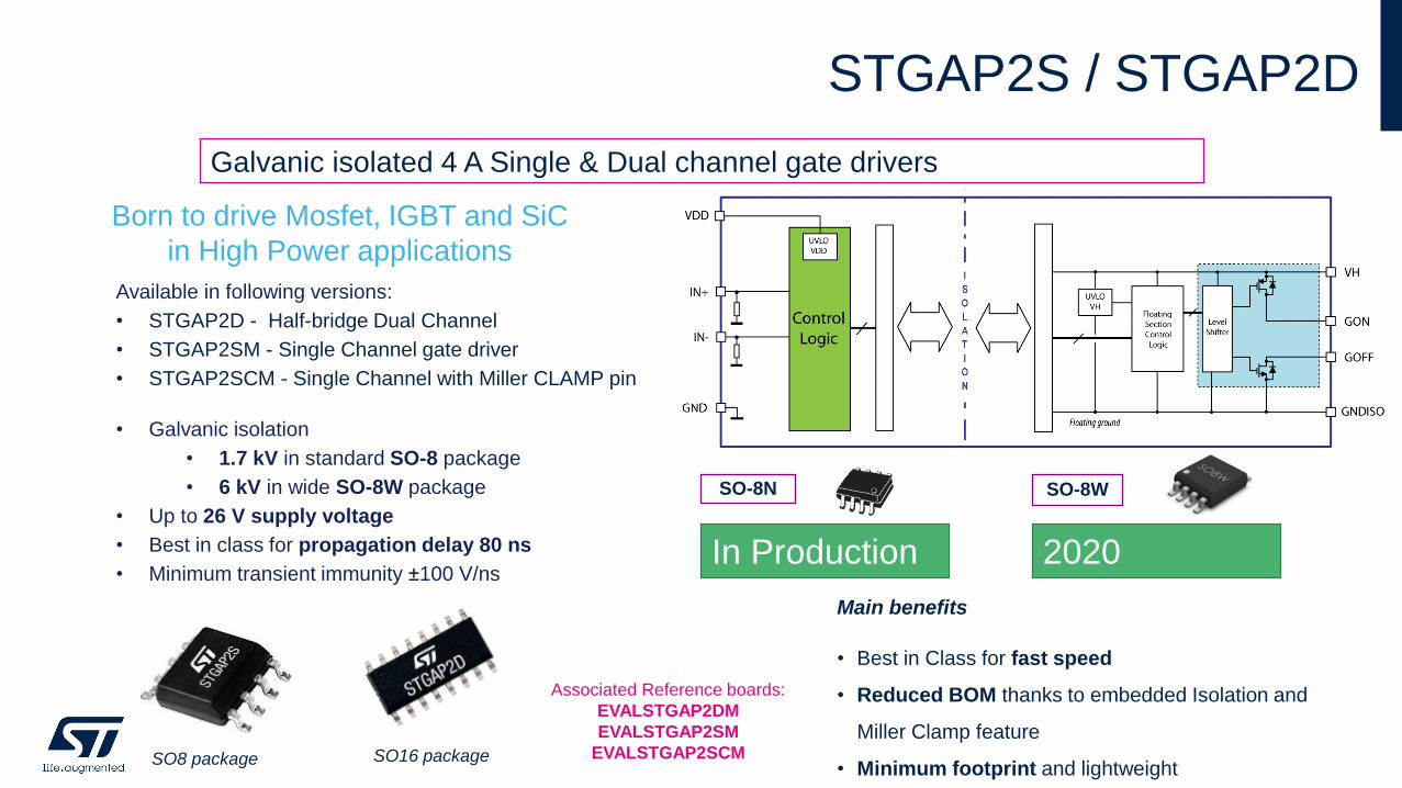
STGAP2S / STGAP2D
Born to drive Mosfet, IGBT and SiC
in High Power applications
Galvanic isolated 4 A Single & Dual channel gate drivers
Available in following versions:
• STGAP2D - Half-bridge Dual Channel
• STGAP2SM - Single Channel gate driver
• STGAP2SCM - Single Channel with Miller CLAMP pin
• Galvanic isolation
• 1.7 kV in standard SO-8 package
• 6 kV in wide SO-8W package
• Up to 26 V supply voltage
• Best in class for propagation delay 80 ns
• Minimum transient immunity ±100 V/ns
Associated Reference boards:
EVALSTGAP2DM
EVALSTGAP2SM
EVALSTGAP2SCMSO8 package SO16 package
• Best in Class for fast speed
• Reduced BOM thanks to embedded Isolation and
Miller Clamp feature
• Minimum footprint and lightweight
Main benefits
SO-8N SO-8W
In Production 2020

Option 2:
Separated sink\source outputs (no Miller Clamp)
SiC MOSFETAbout Driving… STGAP2S
1700 V, 4A gate drivers
Option 1:
Single output and Miller CLAMP
Recommended for SiC MOSFETs in
bridge topologies
5252

SiC MOSFETDynamics: Advantages of Active Miller Clamp
Positive Glitch
-15
-10
-5
0
5
10
15
20
2.11E-05 2.13E-05 2.15E-05 2.17E-05 2.19E-05 2.21E-05
Vgs [
V]
Time [sec]
Vgs with S-OUT
Vgs with AMC
driver configuration
• S-Out: separated output (no Miller Clamp)
• AMC: Active Miller Clamp
𝑽𝑮𝑯 = 𝟏𝟖 𝑽𝑽𝑮𝑳 = −𝟓 𝑽
SCTW35N65G2V
55 mΩ, 650 V SiC MOSFET
Active Miller Clamp is recommended for SiC MOSFETs in bridge toplogies
-15
-10
-5
0
5
10
15
20
1.96E-05 1.97E-05 1.98E-05 1.99E-05 2.00E-05 2.01E-05 2.02E-05 2.03E-05V
gs [
V]
Time [sec]
Vgs off with AMC
Vgs off with S-OUT
Negative Glitch
Q2
Q1
Example: Half-Bridge
Current flow
53
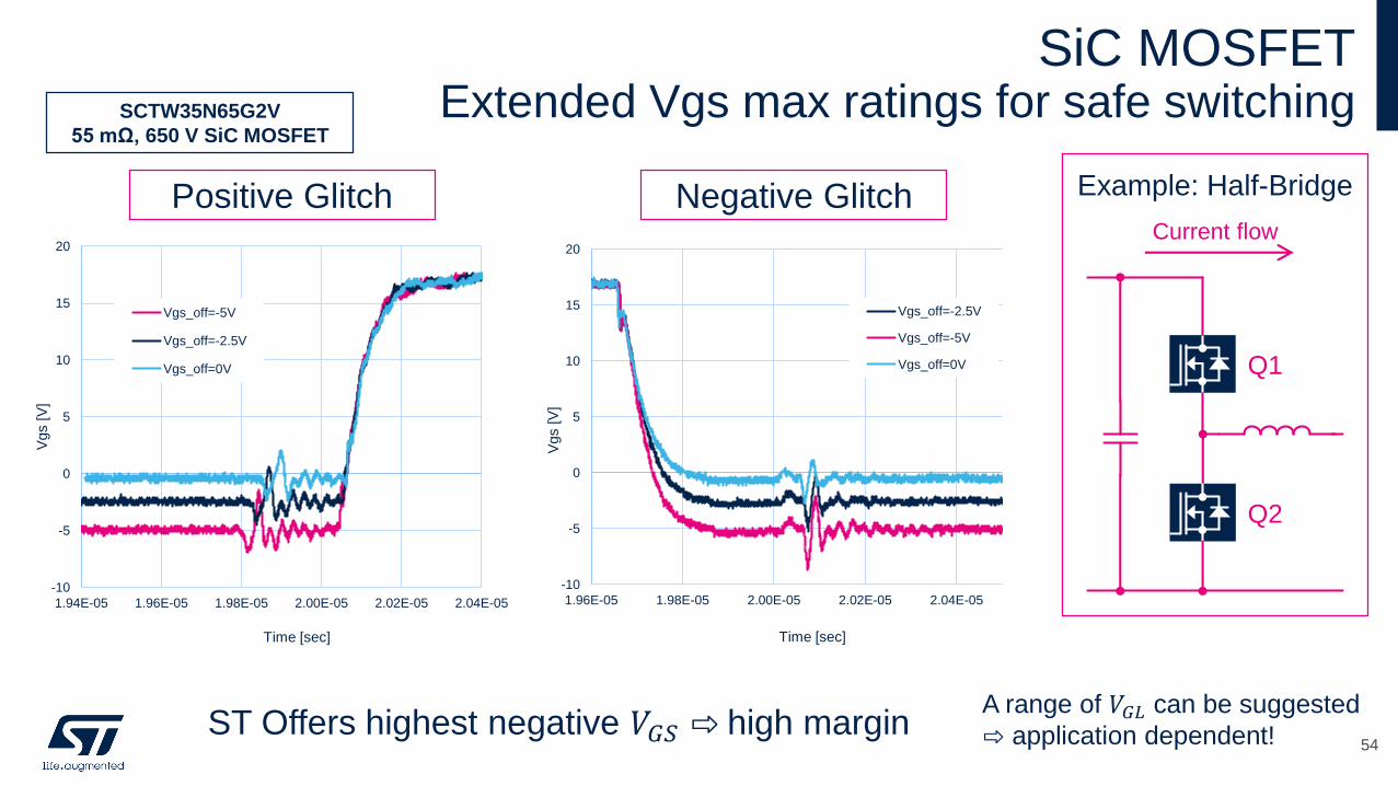
SiC MOSFETExtended Vgs max ratings for safe switching
ST Offers highest negative 𝑉𝐺𝑆 high margin
-10
-5
0
5
10
15
20
1.94E-05 1.96E-05 1.98E-05 2.00E-05 2.02E-05 2.04E-05
Vgs [
V]
Time [sec]
Vgs_off=-5V
Vgs_off=-2.5V
Vgs_off=0V
Positive Glitch
-10
-5
0
5
10
15
20
1.96E-05 1.98E-05 2.00E-05 2.02E-05 2.04E-05
Vgs [
V]
Time [sec]
Vgs_off=-2.5V
Vgs_off=-5V
Vgs_off=0V
Negative Glitch
SCTW35N65G2V
55 mΩ, 650 V SiC MOSFET
A range of 𝑉𝐺𝐿 can be suggested
application dependent!
Q2
Q1
Example: Half-Bridge
Current flow
54
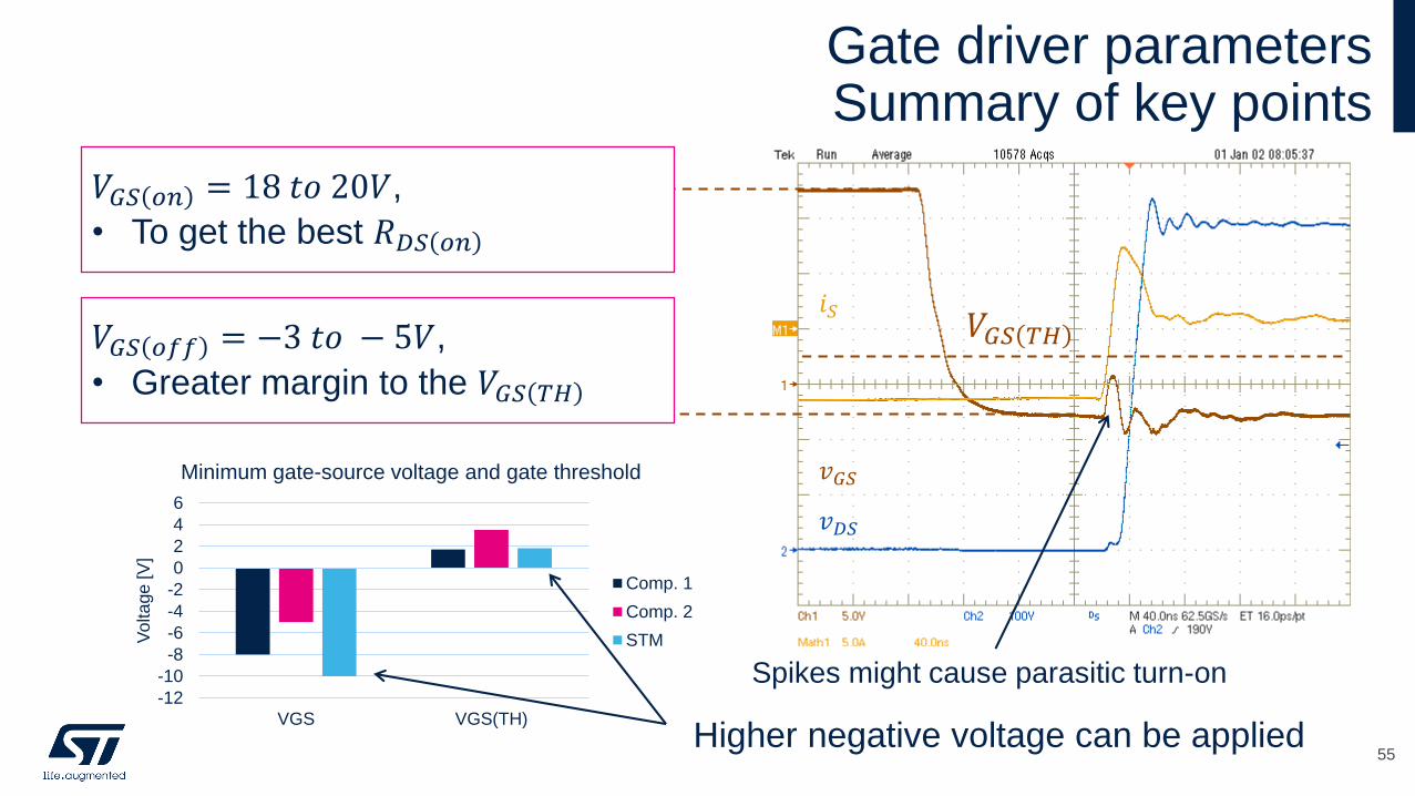
Gate driver parametersSummary of key points
𝑖𝑆
𝑣𝐺𝑆
𝑣𝐷𝑆
𝑉𝐺𝑆 𝑜𝑓𝑓 = −3 𝑡𝑜 − 5𝑉,
• Greater margin to the 𝑉𝐺𝑆 𝑇𝐻
𝑉𝐺𝑆 𝑜𝑛 = 18 𝑡𝑜 20𝑉,
• To get the best 𝑅𝐷𝑆 𝑜𝑛
𝑉𝐺𝑆 𝑇𝐻
Spikes might cause parasitic turn-on -12
-10
-8
-6
-4
-2
0
2
4
6
VGS VGS(TH)
Vo
lta
ge
[V
]
Minimum gate-source voltage and gate threshold
Comp. 1
Comp. 2
STM
Higher negative voltage can be applied55
• Driving a SiC MOSFET is almost easy as driving a silicon MOSFET:
• ST suggest using recommended Vgs , like 18V to get the right RDS(on)
• Adequate current capability to ensure high switching speed
• Turn-off a SiC MOSFET with Negative driving voltage :
• Negative voltage is suggested only for bridge topologies to avoid any possible undesired turn-on due to gate voltage
oscillations (Miller turn-on effect).
• The negative voltage (in the range [-6V,-2V] has an impact on the turn-off switching losses reduction. This of course will
depend on the sinking current driver’s capability.
• To turn-off with a few negative volts (-6V is the minimum recommended) in order to not exceed the max.
• The main aspects influencing switching behavior are:
• Turn-off energy (Eoff) dependence on Rg and VGS-off (negative bias gate voltage)
• Turn-on energy (Eon) dependence on Rg
• Miller effect, which affects Eon and Err (reverse recovery energy)
• Gate drive current requirements
Summary
56

New SiC related evalboards

15kW VIENNA Rectifier
584 Layer PCB (40x36 cm)
*Under Development
Key products
• STNRGPF03* (Digital controller for 3Ph PFC)
• SCTW35N65G2V (6x SiC MOSFET)
• STGAP2S (Galvanic Isolated Gate Driver)
• STPSC20H12D (SiC diodes) , STPS1L30A, STPS2H100A,
STTH1L06A, STPS1150A, STPS2L60A (Schottky and Ultrafast
diodes)
• VIPer26HD (High Voltage Converter)
Main specs• 3-phase, 3-level AC/DC power converter
• Rated nominal output DC voltage: 800 VDC
• Rated nominal input AC voltage: 400 VAC at 50 Hz
• Nominal output power AC/DC: 15 kW
• Power factor, PF>0.99
• Inrush current control and soft start-up
• THD lower than 5% at nominal operation
• Power section based on SiC MOSFETs and diodes:
• High frequency operation (70 kHz)
• High peak efficiency greater than 98%
• Passive element weight and size reduction
ST Demoboard: STDES-VIENNARECT

15kW 3L T-Type Converter PFC
Main specs
• Pout = 15kW @ Vin = 380Vac & Vout =800V
• PF > 0.98 @ 20% load (target)
• THD < 5% @ 20% load (target)
• Ր > 99%
• CCM decoupling current control loop
• Active & Reactive power control
• Grid Connection capability
• Switching frequency = 100kHz
• I_ripple = 2.5A
• VDC_ripple = 10Vpp
Key products
• SCTW40N120G2V (6x 70mΩ 1200V SiC MOSFET)
• SCTW35N65G2V (6x 55mΩ 650V SiC MOSFET)
• STGAP2S (Galvanic Isolated Gate Driver)
• STPS1L30A, STPS2H100A, STTH1L06A, STPS1150A, STPS2L60A
(SiC, Schottky and Ultrafast diodes)
• STS6NF20V (N-channel 20 V, STripFET II Power MOSFET)
• TSV911IDT, TSV912IDT, TSV914IDT (wide-bandwidth rail to rail Op-
Amps)
• STLM20W87F (Analog temperature sensor)
• LD29080DT50R, LD29080S33R, (LDOs)
• VIPer26K (High Voltage Converter)
ST Demoboard: STDES-PFCBIDIR
59

STEVAL-DPSTPFC1 3.6 kW 1-ph Totem-Pole PFC
• Input AC voltage: 85 VAC up to 264 VAC
• Input AC frequency: 45 Hz up to 65 Hz
• DC output voltage: 400 VDC
• Maximum input current: 16 ARMS
• Ambient temperature: tested from 0 °C up to 45 °C
• Peak Efficiency: 97.7 % with 4.7% THD
• Compliant with:
• EN 55015 and IEC 61000-4-11 and IEC 61000-3-3
• IEC 61000-4-5 surge: 4 kV
• IEC 61000-4-4 EFT burst: criteria A @ 4 kV min
• Cooling: forced air cooling with active fan
• Designed for operation with DC / DC converter
• Peak inrush current tuning
Vout
STGAP2S
L400VDC
STGAP2S
N
SCTW35N65G2VSiC MOSFET 650 V, 55 mΩ
TN3050H-12WYSCR Thyristor 30A 1200V
STM32F33460

ST SiC MOSFET/Diode support tools

• Application Notes
• AN4242 – New generation of 650 V SiC diodes
• https://www.st.com/content/ccc/resource/technical/document/application_note/2c/90/d1/db/92/da/49/92/DM00075656.pdf/files/DM0007
5656.pdf/jcr:content/translations/en.DM00075656.pdf
• AN5088 - Rectifiers thermal management, handling and mounting recommendations
• https://www.st.com/resource/en/application_note/dm00437554.pdf
• AN5436 - Thermal behavior and printed circuit board assembly recommendations for STMicroelectronics PowerFLAT
8x8 HV package
• https://www.st.com/content/ccc/resource/technical/document/application_note/group1/01/52/a9/72/04/31/46/44/DM00676401/files/DM0
0676401.pdf/jcr:content/translations/en.DM00676401.pdf
• Simulation Models
• Silicon-carbide (SiC) Schottky diode PSpice models (.lib & .olb)
SiC Diode support tools

• Application Notes
• AN3152 – The right technology for solar converters
• https://www.st.com/resource/en/application_note/cd00264004.pdf
• AN5355 - Mitigation technique of the SiC MOSFET gate voltage glitches with Miller clamp
• https://www.st.com/resource/en/application_note/dm00628522.pdf
• AN4671 - How to fine tune your SiC MOSFET gate driver to minimize losses
• https://www.st.com/resource/en/application_note/dm00170577.pdf
• STPOWER MOSFET finder mobile App for tablets and smartphones (Apple Store, Google Play, Wandoujia)
• https://www.st.com/content/st_com/en/products/mobile-applications/finders-apps/st-mosfet-finder.html
• Simulation Models
• SiC MOSFET PSpice models (.lib & .olb)
SiC MOSFET support tools
63


© STMicroelectronics - All rights reserved.
ST logo is a trademark or a registered trademark of STMicroelectronics International NV or its affiliates in the EU and/or other countries.
For additional information about ST trademarks, please refer to www.st.com/trademarks.
All other product or service names are the property of their respective owners.
Thank you