Embed Size (px)
Citation preview

-
Stanford University Power Electronics Research - Laboratory (SUPER-Lab)
3D printed components for high frequency power converters
Jiale Xu, Emily Hernandez, Wei Liang, Juan Rivas [email protected]
February 1, 2017
Stanford University Power Electronics Research Laboratory (SUPER-Lab) February 1, 2017 1 / 18 Stanford University

Int. Conf vol., no., pp.1,20, 16-18 March 2010. ,-Kolar, J.W.; Biela, J.; Waffler, S.; Friedli, T.; Badstuebner, U., “Performance trends and limitations of power electronic systems, CIPS, 2010 6th
Power density in Converters � Inductors and capacitors
� size ∝ f1 s
� Slow improvements in size and performance � Semiconductors
� Switching loss ∝ fs � Great advances in recent years
� Heatsink: Hard to extract heat from small volumes
” Stanford University Power Electronics Research Laboratory (SUPER-Lab) February 1, 2017 2 / 18 Stanford University

-
Why switching at 10s of MHz? PowerDensity
Frequency
~500W/in3
~50W/in3Conventional
Air-Core
~200KHz ~1MHz ~10MHz ~500MHz
The promise of VHF power conversion Reduced energy storage → Smaller passive components & Faster transient response
J. S. Glaser, et al, ”A 900W, 300V to 50V dc-dc power converter with a 30 MHz switching frequency,” In Proc. Twenty-Fourth Annual IEEE Applied Power Electronics Conf. and Exposition APEC 2009, pp. 1121-1128, 2009.
Stanford University Power Electronics Research Laboratory (SUPER-Lab) February 1, 2017 3 / 18 Stanford University

�
���
��
�
�
-
Very High Frequency Power Electronics
Switching at 10’s of MHz High frequency operation reduces the energy storage requirements of inductors and capacitors. Inductors are small enough to be fabricated with an air-core
Stable over a wide temperature range (No Curie temperature limit) May reduce de-rating requirements (No saturation)
Enable high control bandwidth Reduction of bulk energy storage in high power pulsed applications (i.e radars)
Use PCB to implement inductors Inductances and capacitances can be implemented within the PCB Filters and EMI shielding can also be implemented within the PCB.
Stanford University Power Electronics Research Laboratory (SUPER-Lab) February 1, 2017 4 / 18 Stanford University

�
�
�
�
�
�
�
�
-
Device Switching Loss
+
−
GateDrive
VIN
L
RLoad
vds(t)id(t)
C
t
vds(t) id(t)
t
ploss(t)+
−
GateDrive
VIN
Lchoke LRCR
RLoadC1vds(t)
DOFFT DONT
3.6VIN
Switching loss (hard switching) V-I overlap during device switching Includes device charge removal at turn off (device recovery) Includes device capacitance discharge at turn on
Energy stored at turn off, discharged at turn on (if not ZVS)
Resonant Zero-Voltage Switching reduces switching loss (e.g., Class E)
V-I overlap loss greatly reduced via capacitive snubbing ZVS turn-on avoids capacitive energy dump Only efficient over a narrow load range Device stresses are high for many topologies
Stanford University Power Electronics Research Laboratory (SUPER-Lab) February 1, 2017 5 / 18 Stanford University
��
�
�
�
-
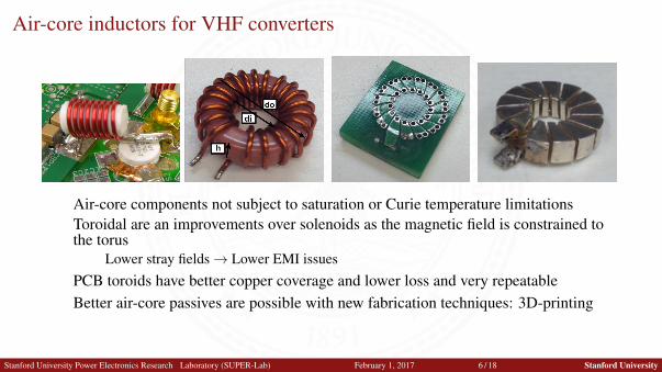
Air-core inductors for VHF converters
Air-core components not subject to saturation or Curie temperature limitations Toroidal are an improvements over solenoids as the magnetic field is constrained to the torus
Lower stray fields → Lower EMI issues
PCB toroids have better copper coverage and lower loss and very repeatable Better air-core passives are possible with new fabrication techniques: 3D-printing
Stanford University Power Electronics Research Laboratory (SUPER-Lab) February 1, 2017 6 / 18 Stanford University

��
-
3D printed passive components
(a) 3D CAD model (b) 3D printed plastic mold (c) cast silver model
Fig.: Steps in the fabrication of a 3D inductor. (a) shows the OpenJSCAD model, (b) shows a translucent plastic model and (c) shows a sterling silver inductor. The 3D inductor has 10nH inductance and its dimensions are OD=18mm, ID=6mm, N=4. Also notice the rounded cross section.
3D printing can overcome limitations of PCB and wire-wound inductors Overhangs, curved surfaces, texture possible
Stanford University Power Electronics Research Laboratory (SUPER-Lab) February 1, 2017 7 / 18 Stanford University

�
-
Path forward
Replacing solenoids with toroids → Printing passives within inner layers of PCB. Top and bottom layers function as EMI shield and heatsink
Stanford University Power Electronics Research Laboratory (SUPER-Lab) February 1, 2017 8 / 18 Stanford University

�
�
�
-
“one turn” inductance
one turn axial direction inductance that can lead to EMI, extra losses on the ground plane Also results in current crowding on the inner ring of the toroid For air core inductors, the “one turn” inductance is comparable in value to the toroidal value
Stanford University Power Electronics Research Laboratory (SUPER-Lab) February 1, 2017 9 / 18 Stanford University

�
-
“one turn” inductance cancellation
We can place two inductors with same dimensions but opposite winding direction vertically stacked to cancel the axial fields.
Stanford University Power Electronics Research Laboratory (SUPER-Lab) February 1, 2017 10 / 18 Stanford University

�
�
��
-
Prototype Implementation
0 50 100 150 200−100
0
100
200
300
400
500
Time [nS]
Vol
ts [V
]
Drain Voltage
MeasuredSimulated
0 50 100 150 200 250−250
−200
−150
−100
−50
0
50
100
Time [nS]
Vol
ts [V
]
Anode Voltage
MeasuredSimulated27.12 MHz, 320 W Dc-dc Converter (170 V to
28 V) Inductors and capacitors implemented with PCB traces
Inductors implemented in FR4 Capacitors implemented using ROGERS laminate (4360G2)
Stanford University Power Electronics Research Laboratory (SUPER-Lab) February 1, 2017 11 / 18 Stanford University
-
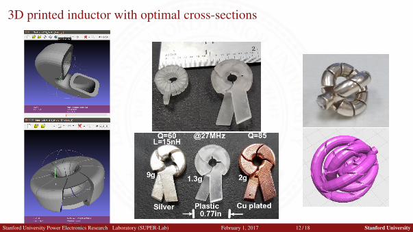
3D printed inductor with optimal cross-sections
Stanford University Power Electronics Research Laboratory (SUPER-Lab) February 1, 2017 12 / 18 Stanford University

-
3D Printed Inductors with Optimal Cross Section
Parameter value units
Scaffold 0.46 gWeight
Plated 0.71 gWeight
Inductance 98 nH(modeled)
Inductance 90 nH(measured)
Q (@ 27.12 MHz) 105(modeled)
Q (@ 27.12 MHz) 94(measured)
Stanford University Power Electronics Research Laboratory (SUPER-Lab) February 1, 2017 13 / 18 Stanford University

�
��
��
-
3D Printed Prototype
+− vds(t)
+
-vgs(t)+
-
LMR
CMR
LF LS CS
RL vload(t)
+
-
VIN
Q1
CP
3D printed
Φ2 Inverter Three inductors connect to MOSFET’s drain node
Single scaffold for the three inductors → 1.13 g Printed using Form 1+ SLA 3D printer (Formlabs)
High frequency → small inductors Good power density
Stanford University Power Electronics Research Laboratory (SUPER-Lab) February 1, 2017 14 / 18 Stanford University

-
3D Printed Prototype
+− dc/rfVIN
MatchingNetwork
Gas propelant flow
PermanentMagnetRf coil
Stanford University Power Electronics Research Laboratory (SUPER-Lab) February 1, 2017 15 / 18 Stanford University

���
�
-
3D printed inductors
0.5 inch
1.3 inch
Advantage of the 3D printed toroidal inductors Obtaining higher power density than the one with solenoidal inductors Reducing a leakage flux of solenoidal inductors (decreasing inductive heating and EMI)
Electrical characteristics depend on surface finishing and printing quality
Stanford University Power Electronics Research Laboratory (SUPER-Lab) February 1, 2017 16 / 18 Stanford University

��
-
Highly Integrated Modular LED Luminaire Contract# DE-EE-0007629
Exploring methods to incorporate PCB Incorporate high permeability material fabrication techniques to the converters in our 3D printed designs operating at 100’s of kHz
In collaboration with General Electric
Stanford University Power Electronics Research Laboratory (SUPER-Lab) February 1, 2017 17 / 18 Stanford University

����
-
Acknowledgments
This work has been possible through the support of: NSF Award Number: ECCS-1439935 The Precourt Institute for Energy Department of Energy DE-EE-0007629
Stanford University Power Electronics Research Laboratory (SUPER-Lab) February 1, 2017 18 / 18 Stanford University