Embed Size (px)
Citation preview

Sta te -o f - the -a r t of non- destructive measurement of sub-surface material properties and damages
E. Brinksmeier*
The possibilities of common non-destructive measuring techniques are reviewed in this paper for their applications in precision engineering. The grazing X-ray technique is believed to be a powerful improvement of the conventional X-ray techniques under both the diffraction mode and the fluorescent mode. Information of the crystallographic structure and chemical composition can be obtained to a nanometre resolution. Ultrasound can be used in scanning acoustic microscopy to give information on the physical or even chemical nature of superficial layers. Raman spectroscopy has now become an important tool for studying superficial structures, chemical composition and stresses in crystalline and amorphous materials: it is recommended to use this method especially for the investigation of monocrystalline silicon and germanium. The instrumented microindentation technique is a quasi- non-destructive technique for evaluating mechanical material properties like hardness and Young "s modulus in a nanometre range. It can be used on any material that does not require special surroundings like a vacuum. Photothermal microscopy has been developed recently for the non- destructive testing of the local thermal properties of materials. By using the Mirage effect and its local measurement above the surface, a non-destructive depth profil ing of surface damages can be obtained.
Keywords: non-destructive measurement, sub-surface damage, X-rays, scanning acoustic microscopy, Raman spectroscopy, microindentation techniques, photothermal microscopy
The requirements of higher precision and increasing miniaturization in a wide range of manufacturing activities afford new capabilities in machining, positioning, control and metrology to nanometre tolerances.
The machining processes which are necessary to produce parts with the highest possible accuracies are defined as precision and ultra- precision machining. The fundamentals and applications of these new technologies have been widely discussed by Taniguchi, McKeown and Franks 1-3.
Much successful work has been done during the last few years to improve the necessary dimensional and surface metrology for such parts. In particular, the rapid developments in tunelling microscopy have enabled scientists to widen their views by now including atomic dimensions.
Precision and ultra-precision machining, however, do not only produce parts with dimensional properties. It can be also expected, and has been proved, that the machining processes
* Institute for Production Engineering, and Machine Tools (IFW), University of Hannover, Schlosswender Strasse 5, 3000 Hannover I, FRG
influence the physical and chemical state of the surface and sub-surface layers. These properties / damages / stresses may influence the part's topography, dimensional accuracy and the functional behaviour under working conditions.
Up to the present, few results are known from measuring and evaluating sub-surface damage after precision and ultra-precision machining. One reason for this may be the lack of knowledge of which non-destructive measuring techniques can be applied in the testing of the sub-micrometre surface range. Therefore, this paper reviews the possibilities of common measuring techniques for their applications in precision engineering. Also, the potentials of new techniques like grazing incidence diffraction, Raman spectroscopy, scanning acoustic microscopy, and microindentation techniques are introduced.
Mater ia l removal in precision and ultra- precision machining
The requirements of non-destructive measuring methods for evaluating surface and sub-surface integrity have to be derived from the workpjece material's behaviour when material is removed and
PRECISION ENGINEERING 0141-6359/89/040211-14/$03.00 © 1989 Butterworth & Co (Publishers) Ltd 21 1

Brinksmeier--non-destructive measurement of sub-surface material properties
from the functional requirements of the produced surface.
Little knowledge exists about the actual progress in material removal when machining with a very low depth of cut. However, several assumptions and conceptual models have been set up4 8. A model with reference to the surface topography and accuracy of the workpiece has been introduced by Konig 5. The different orientations of the individual grains between the grain boundaries result in a change of the cutting force equilibrium because cutting depends on the shearing direction of the crystallographic planes. Due to the fixed stiffness of the system, the alternating Young's modulus of the grains results in surface undulations of the machined base material. It is therefore proposed to develop nanocrystalline materials, the grain sizes of which are considerably smaller than the chip thickness in machining.
Supposing that the stiffness and the accuracies of the tool and the base material are high enough not to cause problems with the imbalance of internal texture and surface roughness, a physical model for the cutting mechanism, introduced by Hashimoto et al 6 can be realized (Fig 1 ).
A cutting mechanism that corresponds to a desired surface roughness of about 0.01 /~m has to cope with microcrystalline particles and precipitations of the order of 0.1 #m, with dislocations of the order of 0.01 pm, and the motion of ions, electrons and atoms of the order of 0.001 pm. As the cutting proceeds, the material will be plastically deformed, triggered by precipitation, increasing dislocations, voids etc. It can be seen from Fig 1 that the cutting process leads to a multiplication of defects, a considerable number of which wil l remain in the sub-surface layers and will thus influence the integrity of the surface. Those defects are not only dislocations but also fine cracks, cavities, delaminations and cracked particles which may have lost their binding power to the base material.
A changed surface integrity may also result from a 'plastic fluidization' of the machined base material 6-8 due to high local pressure. A surface generation by plastic f low can be achieved for all work materials and is independent of the type of mechanical machining;.
Dislocation V W chip growth ~ ~ k
terminated f ~
- - .I. I "~--~. ~ - Voids Cavity /v'~'C " °/ ~o
I v >,% .7/%. 'T T - / T ¢ - r
\Atoms ov / 'ov '1 . ~ " Dislocation growth ~ /
Crystal grain~ o v , , ~ I T P boundary - - I Precipitation T p ~ / r 'ecipitation T p ~ _ . _ j ~ . ~ . . ~
Fig 1 Imperfections in materials that influence ultra-high precision cutting (from Hashimoto )
Surface i n t e g r i t y in precision and u l t r a - p r e c i s i o n machining
Generally, we can distinguish between mechanical, thermal and chemical impacts generating the state of surfaces and sub-surfaces in machining. These individual impacts, which may occur in a continuous or intermittent mode, all influence to different degrees the material's physical properties. Mechanical impacts wil l result in strain hardening, plastic deformations, and compressive residual stresses whereas thermal impacts may result in soft annealing, tensile workpiece stresses and phase transformations. Chemical impacts may be of growing importance in precision and ultra-precision machining. Typical changes of the workpiece surface may be due to chemically-induced cracks, selective etch and changing of composition by diffusion or ion implantation.
Knowledge of the surface and sub-surface properties of the base material is of great importance due to their influence on the functional behaviour of the surface, the obtainable machining accuracy and also due to the demands for knowledge about the material removal mechanism.
It is agreed that not only the geometrical but also the physical properties of a machined surface have influence on the surface's function. This is true for the fatigue strength under dynamic loading, the sensitivity to corrosion, the surface behaviour under wear, critical sliding and rolling loads, and the applicability of a surface for coating. Also, magnetic properties (video recorder heads) and electronic properties (Si-wafers) depend on the microstructure of the material and the distribution of chemical elements in the surface layers.
From conventional machining it is known that residual workpiece stresses will influence the geometry and the accuracy of a machined part. This will be similar or may even be stronger in precision and ultra-precision machining: the requirements on dimensional tolerances are ultimately high. With the knowledge of the residual stress state, a possible workpiece deflection can be estimated. Also, the determination of microcrystalline grain orientation, boundaries, voids and precipitations is of interest in ultraprecision machining.
Most of the physical workpiece properties and their changes after machining can neither be estimated nor calculated. Therefore, these properties have to be measured using non-destructive techniques with high spatial resolution. For meeting the requirements on ultra-precision machining a 'high spatial resolution' may be interpreted as a resolution between the dimensions of an atomic bit and, approximately 1 pm.
Non-destructive measurement of surface and ~ub-surface properties
If superficial workpiece properties have to be measured, these properties must be distinguished clearly from the measuring quantities actually available from a certain technique. In other words, some of the properties can be measured directly, most of them can, however, only be measured in an
212 OCTOBER 1989 VOL 11 NO 4

Brinksmeier--non-destructive measurement of sub-surface material properties
::::::::::::::: Example ::::::::::::::::::::: : :::::::::..........................: :: :::::::: ::::::::::::::::::::: [ 1 iiiiiiiil I iiiiiiiiiiiiiiiiii]iiiiiiiiiii!iii
Measuring quant ty :,iN 1 ~ - - ~ d ::i::;::i::i::i::i::i!iiiiiiiiiiiiiiiiiii . _ .
Direct measurement I iiiiii~H EIEIIi Eiiiiiiiiiiiiiiiii::i::i::i::i::i::i::i::i::iii:: r t Indirect :::: :: :: :: :: :: :: :: :: :: :: :::: :::: ::: :: :: :: :: :: :: :: :: :: :: :: :: I: ::::: :::::: ::::: :::: :: :: :: :: :: :: :: :: :::::: :: : :: : : : : : :: :: :: :: ::
1 measurement ::::::::::::::::::::::::::::::::J::::::::::: :::::: i::::::::::::::::: • " i:i:i:i ::':':':':+:':':':':" f f : i ; i : : : : : : : : :: : : : : : : : : : :::::::::::: I :':':': . . . . . . . . . . . :::::::::::::::::::::::
Physical/empirical model
Workpiece properties
Structural/ chemical
• Structure
- size and orientation of grains
-- atomic distances - dislocations - lattice imperfections - interstitial atoms - impurities • Chemical state - composition - concentration
profiles
Physical
• Strains
• Stresses
• Electrical/thermal conductivity
• Magnetic properties
• Micro-cracks, voids
F " ' • • " • " • " • " " "
HV = ~, .iiiiiiiiiii::iiiiiiiil. :::::::::::::::::::::::::::::::::::::::::::::::::::::::::::::::::::::::::::::
Mechanical
I • Strength
• Fatigue
• Young's modulus
• Deformations
• Friction number
Fig 2 Direct and indirect measurement of different types of workpiece properties
indirect way. The latter condition therefore, will require additional physical or empirical models in order to correlate the measuring quantities with the unknown values of the structural, chemical, physical, and mechanical properties, as outlined in Fig 2.
For engineering materials with technical surfaces the interest in measuring the state of surfaces is mainly focused on physical properties as they will determine the function. These properties however, may be finally derived from the metallurgical and chemical state of the material. Therefore, it may be of interest to measure also the composition, structure and chemical state of surfaces. This will be necessary if a better understanding of processes at a microscopic or atomic level is desired.
For the investigations into structural and chemical properties several methods have been developed. Most of them require ultra-high vacuums to prevent contamination and enable the use of particle or photon irradiation. When the sample is bombarded, secondary particles or photons are emitted from the surface• Alternatively, irradiation can be scattered from the surface with a measurable loss of energy• There are four main types of primary bombardment and they use photons, electrons, ions and fast atoms (Fig 3). Within the four possibilities lie the various methods used in chemical and structural surface analysis. The surfaces probed by these different techniques vary in depth from the uppermost atomic layer to several tens of
i Photons I Photoelectrons< ;~\_ate_6~ ~ a r ~/"/" l" a~/
Auger electrons %, ~1~ ~f~#e~V,Secondary and : ~ X i J ~ DaCK scatterea e,ectrons
Secondar~ ions " ~ / scR t~ It eeCdt ee rde :trdo n s
Scattered ions ~ i iiiii!iiiiiiiiiiiiil . ~ Auger e i ect r o n s
I ions ! i i i i i i i i i i i i i ~ - ' = ~ Electrons I Electrons " ~ iiiilili~!~!i~i~!i t --LI_ ~ Diffracted
iiiiiiii :: :: :: :: i ~i "-r,~, "-~ -.~ electrons Neutral atoms etc~ :i:i:i:~:~:;:~:;:!:] ~-~# ~, Secondary and
X-rays Vacu~ ~ace backscattered electrons ~, Secondary ions
Neutral atoms Secondary electrons
I Fast atoms J
Fig 3 Interactions used in surface analysis of the structural and chemical state (from I. Drummond)
Angstroms. This ability to analyse structure and chemical states just beneath the surface will be particularly necessary in studies of semiconductors when determining the surface chemical stoichiometry, ordering, and orientation of the surface with the identification of impurities 9.
With so many different techniques now available to laboratories, it is not possible to describe each method and its capability in detail in this paper. As most techniques also require an ultra- high vacuum surrounding without any contamination this may be a considerable limitation to their applicability to engineering surfaces of real materials of interest. Therefore only a few selected methods will be discussed within this paper.
Some of the structural, chemical and physical, surface and sub-surface properties, which are of interest in precision and ultra-precision machining, are outlined in Fig 4.
It can be seen that the dimensions cover the range from 1 nm to more than 1 mm. None of the available measuring techniques is effective in identifying structural parameters over the full range of dimensions. This can only be reached by using different techniques with different types of physical
-$
E 8 (13
10-10
I I I 1 I [ Micro/macro stresses ( I, II, I I I type) [
: : : : : : : : : : : : : : : : : : : : : : : : : : : : : : : : : : : : : : : : : : : : : : : : : : : : : : : : : : : : : : : : : : : : : : : : ::::::::::::::::::::::::::::::::::::::::::::::::::::::::::::::::::::::::::::::::::::::::::::::::
Dislocations Texture/anisotropy I :::::::::::::::::::::::::::::::::::::::::::::::::::: ::::::::::::::::::::::::::::::::::::::::::::::: i:!:!:i:::l :::::J I
Lattice imperfections E~rain size ::::::::::::::::::::::::::::::::::::::::::::::::: ::::::::::::::::::::::::::::::::::::::::::::::::::::::::::::::: I
Precipitations Inclusions ::::::::::::::::::::::::::::::::::::::::: ~
Pores Ato m I: :::::::::::::::::::::::::::::::::::::::::::::::::::::::::::::::::::::::::::'
distances Blochwalls ~ ~ void I
10 8 10-6 10-4 10-2
Linear dimension, m
Fig 4 Linear dimensions of structure and defects 7o
PRECISION ENGINEERING 213
Brinksmeier--non-destructive measurement of sub-surface material properties
S z
10-10
Ultrasonic scattering :::::::::::::::::::::::::::::::::::: 1 Absorpt ion echo - defect detect ion
Sound veloci ty Ultrason c microscopy :::: :.:.:;:::::.!..-:-,.::~: !:: ::ii: ::.:,!.:,:, • ~ -. . ~ ~!~ ~:: ::::: :.i , i
Photo opt ic ultrasound
Dynamic micromagnetic, eddy current
Micro Raman s3ectroscopy Current per turbat ion
T h e r m o f o r c e Micro r ad io - a n d t o m o g r a p h y :::::::::::::::::::::::::::::::::::: .: : : : .: ,: : : : . : - : . : . : . : . : - . , : . . . : : t : : : . : . : : : : :-:.:.:1
Mic ro radio - and tomography I I I I ~ . ' . : - : ~ , ~ . - . . , , . I x-ray dif!raction,/fluorescence ] ~
::::::::::::::::::::::::::::::::::::::::::::::::::::::::::::::::::::::::::::::::::::: ; : : : ; : ; : ; : : : ; : ; : ; : : : : : ; : ; : ; : : : . : . : ~ . : . : . : ~ - ' , ' ~ ,'.
I I I I I I I I 10-8 10-6 10-4 10-2
Linear dimension, m
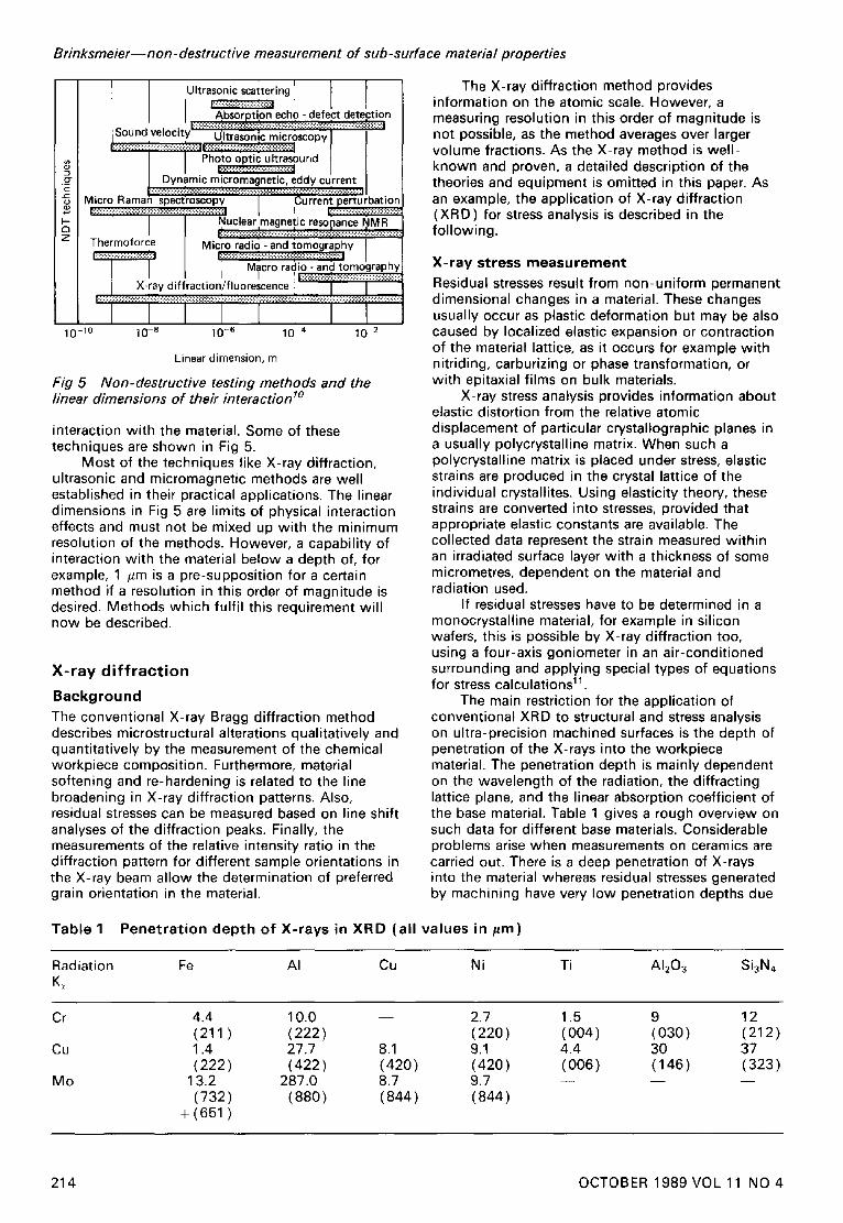
Fig 5 Non-destructive testing methods and the linear dimensions of their interaction 1°
interaction with the material. Some of these techniques are shown in Fig 5.
Most of the techniques like X-ray diffraction, ultrasonic and micromagnetic methods are well established in their practical applications. The linear dimensions in Fig 5 are limits of physical interaction effects and must not be mixed up with the minimum resolution of the methods. However, a capability of interaction with the material below a depth of, for example, 1 /~m is a pre-supposition for a certain method if a resolution in this order of magnitude is desired. Methods which fulfil this requirement will now be described.
X - r a y d i f f r a c t i o n
Background The conventional X-ray Bragg diffraction method describes microstructural alterations qualitatively and quantitatively by the measurement of the chemical workpiece composition. Furthermore, material softening and re-hardening is related to the line broadening in X-ray diffraction patterns. Also, residual stresses can be measured based on line shift analyses of the diffraction peaks. Finally, the measurements of the relative intensity ratio in the diffraction pattern for different sample orientations in the X-ray beam allow the determination of preferred grain orientation in the material.
The X-ray diffraction method provides information on the atomic scale. However, a measuring resolution in this order of magnitude is not possible, as the method averages over larger volume fractions. As the X-ray method is well- known and proven, a detailed description of the theories and equipment is omitted in this paper. As an example, the application of X-ray diffraction (XRD) for stress analysis is described in the following.
X-ray stress measurement Residual stresses result from non-uniform permanent dimensional changes in a material. These changes usually occur as plastic deformation but may be also caused by localized elastic expansion or contraction of the material lattice, as it occurs for example with nitriding, carburizing or phase transformation, or with epitaxial films on bulk materials.
X-ray stress analysis provides information about elastic distortion from the relative atomic displacement of particular crystallographic planes in a usually polycrystalline matrix. When such a polycrystalline matrix is placed under stress, elastic strains are produced in the crystal lattice of the individual crystallites. Using elasticity theory, these strains are converted into stresses, provided that appropriate elastic constants are available. The collected data represent the strain measured within an irradiated surface layer with a thickness of some micrometres, dependent on the material and radiation used.
If residual stresses have to be determined in a monocrystalline material, for example in silicon wafers, this is possible by X-ray diffraction too, using a four-axis goniometer in an air-conditioned surrounding and applying special types of equations for stress calculations 11
The main restriction for the application of conventional XRD to structural and stress analysis on ultra-precision machined surfaces is the depth of penetration of the X-rays into the workpiece material. The penetration depth is mainly dependent on the wavelength of the radiation, the diffracting lattice plane, and the linear absorption coefficient of the base material. Table 1 gives a rough overview on such data for different base materials. Considerable problems arise when measurements on ceramics are carried out. There is a deep penetration of X-rays into the material whereas residual stresses generated by machining have very low penetration depths due
Table 1 Penetrat ion depth of X-rays in XRD (al l values in pro)
Radiation Fe AI Cu Ni K~
Ti A I 2 0 3 S i 3 N 4
Cr 4.4 10.0 (211 ) (222)
Cu 1.4 27.7 (222) (422)
Mo 13.2 287.0 (732) (880)
+ (651)
8.1 (420) 8.7 (844)
2.7 1.5 9 12 (220) (004) (030) (212) 9.1 4.4 30 37 (420) (006) (146) (323) 9.7 - - - - - - (844)
214 OCTOBER 1989 VOL 11 NO 4

Brinksmeier--non-destructive measurement of sub-surface material properties
20
! D ¢O
"O
n -
-20
-40
-6o
-80
-100
-120
-140
-160
Fig 6
CrK~ (2p = 12/~m) /
I - -
rlace grinding
/ / °f Smidia 3N~l'whee I
I I I I
40 0 10 20 30
Cutting speed (Vc), ms-1
Residual maching stresses in Si3N 4 ceramic, measured by two different radiations (surface measurements)
- - 0
50
to the hardness of the material. These problems can be demonstrated by measuring surface stresses using two different types of radiation (Fig 6).
Thus, it can be concluded that conventional X-ray diffraction can be applied in precision engineering. However, if depth profiling of structural parameters and stresses with a resolution below 1 /~m is desired, conventional XRD cannot be used.
G r a z i n g i n c i d e n c e X - r a y dif fract ion For smooth surfaces of polycrystalline materials the problem of the large penetration depths in conventional XRD can be overcome by the application of a recently developed special diffraction technique. The grazing incidence diffraction, an emerging new technique, can be used to obtain structural details and identification of phases of surface layers and films with a thickness ranging down to a few atomic layers 12.
The principle of this technique is based upon the fact that the refractive index of solids in the range of X-ray frequencies is less than one. Therefore, specular (or quasi-total) reflection from surfaces occurs for incidence angles of about a tenth of a degree. At such angles X-ray waves penetrate to very shallow depths in the solid. The depth depends upon the material and the X-ray wavelength and is about a few nanometres. More than 98% of the beam is reflected by superficial layers. By setting the incidence angle at the critical value of reflection, then increasing it step by step, one can probe layers of increasing thickness and analyse their chemical composition or their crystallographic structure by means of diffraction or fluorescence experiments. Fig 7 shows a schematic representation of the grazing incidence diffraction (GID). The angle of incidence is typically chosen between the critical angle of total reflection (0.5-1 °). Instead of conventional X-ray tubes, a source of synchrotron radiation can also be used. A synchrotron source has unique qualities that can be used in diffraction experiments. It produces high- power X-rays, extremely small divergence in the vertical direction, almost unlimited choice of wavelength and linear polarization. The disadvantage, however, is that there are no transportable sources available.
l ~=0° I ~ X ~ , ~ - I , , ~ D etector
~ ~ i / ~ ; i f f r a c t e d X-ray 4T ~ I / , / ~ " X-rays source , ~ 2~
I / I " @ Primary Sample
beam
ConventionaIBragg I
diffraction
I 4:--/=0o I
, ~ "~. J'" ,~Detector
- \ ~ Primary beam
X-ray
Osource_r synchrotron/_7__ =./Divergencel0#mGrazingSlit angle ~ ~ x , "//~xDetector ~ ~ d i f f r a c t i o n , G i D G razing incidence
. I I 0~< 1 ° V 2ehkl --..-
/ . t beam
Sample Beam divergence 0"005° Grain does not
contribute to diffraction Fig 7 Grazing incidence diffraction
PRECISION ENGINEERING 215
Brinksmeier--non-destructive measurement of sub-surface material properties
In Ref 13 GID was used to record diffractograms after friction tests on polycrystall ine titanium and also on chemical deposited films• A film with the composit ion Ni74B26 which is normally amorphous, was submitted to such tests under a pressure of 10 MPa, to study its eventual crystallization induced by strains and temperatures. In some cases partial crystallization was effectively observed ( Fig 8). However, this effect was very superficial since crystallites were removed from the friction track after subsequent passes ( running- in of surface). The analysed depth was less than 1 50 nm. Because the sample area irradiated by X-rays is very wide, the width of the area contr ibuting in diffraction was limited by the use of radial slits between the detector and the sample.
Beside the 20-~? scan for studying lattice parameters, an additional omega-scan (specimen rotation around a vertical axis) provides information about the orientation spread of superficial lattice planes 14.
The possibil ity of measuring the residual machining strains/stresses by using GID has not yet been investigated. Fig 7 shows that there are only some grains beneath the surface which fulfil the diffraction condit ions for a given Bragg angle. The specific orientation of these grains represents the angle of exposure ~ which has to be changed step by step when using the mult i-angle technique. This angle is normally set by an incremental 0 rotation of the specimen as shown in the upper part of Fig 7. Such a procedure is not possible using GID because this would bring the grazing angle out of its small range. However, if a so-called ~ arrangement of the goniometer would be used where the angle of exposure is set by a sample rotation in a plane perpendicular to the measuring plane, the grazing angle wil l become unchanged. This experiment should permit mult i-angle stress measurements in superficial layers in the nanometre range. A pre- supposit ion is that a f ine-grained polycrystall ine material and high power X-ray sources (or synchrotron sources) wil l be used.
180 150 120
.~ 90 ~ 60
E 3O
0
180 150
~ 120
~: 90
g 6o E 30
0
Fig 8
Chemical 1~1i74 B26 I I °urt friction passes
~ - ~ ~ ~ _Friction of a m . _ orphous / P~Ni~Bsta/)hzat'°l n " ~ Ni74B26 I ] [ ' i ~ " I ~ • Normal load : 1N
• Spherical friction pin • Motion speed : 0.5 mms -1
GI D with synchrotron radiation • X=0.154nm
I " Analysed depth < 150 nm Chemical Ni74B26 I (amorphous) Ten
iciion passes I
40 44 48 52 Diffraction angle (20), degrees
GID diffraction of an amorphous film after friction (from Pons, Megtert, Pivin)
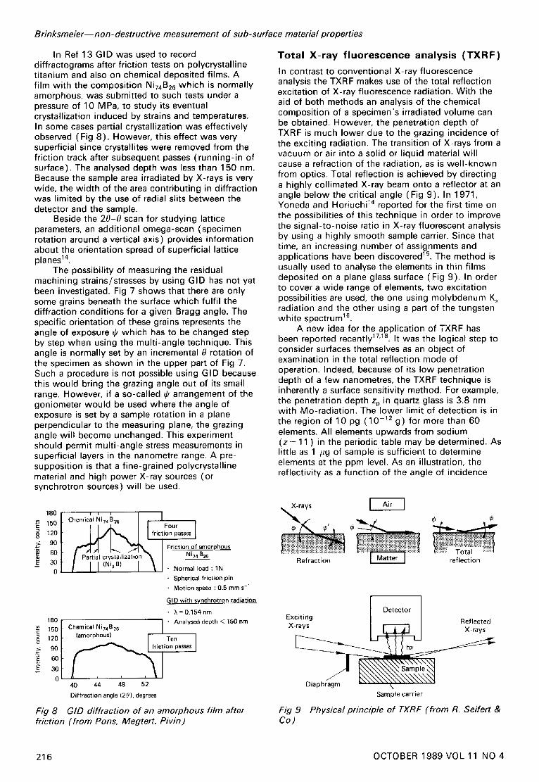
Total X-ray fluorescence analysis (TXRF)
In contrast to conventional X-ray fluorescence analysis the TXRF makes use of the total reflection excitation of X-ray fluorescence radiation. With the aid of both methods an analysis of the chemical composit ion of a specimen's irradiated volume can be obtained. However, the penetration depth of TXRF is much lower due to the grazing incidence of the exciting radiation. The transition of X-rays from a vacuum or air into a solid or l iquid material wi l l cause a refraction of the radiation, as is wel l -known from optics. Total reflection is achieved by directing a highly collimated X-ray beam onto a reflector at an angle below the critical angle (Fig 9). In 1971, Yoneda and Horiuchi TM reported for the first time on the possibilities of this technique in order to improve the signal-to-noise ratio in X-ray fluorescent analysis by using a highly smooth sample carrier. Since that time, an increasing number of assignments and applications have been discovered 15. The method is usually used to analyse the elements in thin films deposited on a plane glass surface ( Fig 9). In order to cover a wide range of elements, two excitation possibilities are used, the one using molybdenum K~ radiation and the other using a part of the tungsten white spectrum 16.
A new idea for the application of TXRF has been reported recently 17'1s. It was the logical step to consider surfaces themselves as an object of examination in the total reflection mode of operation. Indeed, because of its low penetration depth of a few nanometres, the TXRF technique is inherently a surface sensitivity method. For example, the penetration depth zp in quartz glass is 3.8 nm with Mo-radiation. The lower limit of detection is in the region of 10 pg (10 -12 g) for more than 60 elements. All elements upwards from sodium (z = 11 ) in the periodic table may be determined. As little as 1 /~g of sample is sufficient to determine elements at the ppm level. As an illustration, the reflectivity as a funct ion of the angle of incidence
~ ays
lii il i ii.,..t ii!i Refraction I Matter I reflection
I Detector ExcJtmg Reflected X-r:~s L [ ~ J X-rays
utapnragm \ Sample carrier
Fig 9 Physical principle of TXRF (from R. Seifert & Co)
216 OCTOBER 1989 VOL 11 NO 4

Brinksmeier--non-destructive measurement of sub-surface material properties
1000
100 == "o
.o_ =
10
#.
Fig 10
0 2 4 6 8 10 12
Angle of incidence ((~), min
Results of TXRF used on a silicon wafer
.00
-%
0 .66 ....- II
0 . 3 3 [~
ee"
and the values for the corresponding penetration depths for a silicon wafer are given in Fig 10 (See Ref 17).
The depth of penetration is below 10 nm which permits analysis of surface contaminations with an ultimately high degree of resolution in superficial layers. As an example, it was possible by this method to probe 1011 Ni atoms which have been implanted into the surface of a silicon wafer within a depth of 50 nm (See Ref 18). At the moment, there is no other method available which is able to do the same task.
The potential of the TXRF surface analysis is believed to go far beyond the determination of impurities in wafers. Possible applications are also the examination of concentration profiles in near surface layers. Using a white spectrum of exciting radiation the penetration depth can be varied due to the dependence of the critical angle of incidence on the wavelength 18. Thus, concentration profiles in the nanometre range can be obtained non-destructively.
Ultrasonic methods
In contrast to X-ray techniques whose spatial resolution is less than 0.1 mm 3, the ultrasonic methods integrate at least over a section of 100 mm 3 because of sound beam diameters and sound paths dimensions 1°. The most promising application of ultrasonic techniques is the characterization of the volume of components, but by exploiting surface waves, it is also possible to characterize surface layers down to a depth of about 0.1 mm. In precision and ultra-precision engineering, ultrasound may be used to study bulk effects. Surface properties in the nanometre scale are not detectable.
Micromagnetic methods
Micromagnetic methods can only be used in combination with ferrous base materials. This unavoidable prerequisite limits the use of these methods in precision engineering as non-ferrous and ceramic materials have to be machined in the majority of cases. Nevertheless, some applications in microengineering will afford ferrous base materials which permits the use of micromagnetic techniques for non-destructive testing.
The ferromagnetic state of materials reacts very
sensitively to changes of microstructural parameters and stress states. If the specimen has a wel l-known and simple geometry, one can demonstrate these reactions in characteristic changes of the hysteresis loop. In practice, however, the B ( H )-loop cannot be measured in the set-up technique which is necessary for analysing surface phenomena on a specimen. Therefore, different magnetic measuring quantities, like coercivity, Barkhausen noise and incremental permeability have been developed which can be measured in the set-up technique. The fundamentals of micromagnetic methods have been summed up in Ref 10. Fig 11 shows the different signal characteristics of the magnetic Barkhausen noise and the incremental permeability. For the application of both quantities it is important to know that the analysing frequency and the exciting frequency, respectively, determine the penetration depth of the measurement. This relation is also outlined in Fig 11. The minimum depth is determined by the maximum attainable frequency which is estimated to be 10 MHz for the Barkhausen noise and 30 MHz for the incremental permeability. This limits the minimum analysing depth in a ferrous material to 10/~m and 1-5/~m respectively. The local resolution depends on the design of the transducers used and can be reduced to a measuring diameter of about 0.1 mm.
A big advantage of micromagnetic measuring methods is the short measuring time - far below one second. The electronic devices are relatively cheap and allow structured investigations in different depths below the surface just by changing the frequency. These advantages make this measuring technique very well suited for industrial applications. However, a disadvantage is the necessity to calibrate the measurements carefully in order to separate the multi-parameter influences of the material from the measuring quantities. The spatial resolution of these techniques allows an application in precision engineering. A use in ultra-precision engineering is not in sight as the resolution below the surface will not be possible down to below 0.1 /~m.
Scanning acoustic microscopy
Scanning acoustic microscopy comprises several different techniques for the measurement of material properties near the surface. The most important techniques have been recently reviewed by Balk 19. Individual developments and applications on machined surfaces are reported in Refs 19-22.
The principle of scanning acoustic microscopy is based upon the fact that the generation and propagation of acoustic waves, both in the sound and in the ultrasound regimes, are strongly affected by various material parameters such as elastic, thermal, electric and magnetic properties. Accordingly, local variations of each of these quantities can give information on the physical or even chemical nature of the region which the acoustic wave is generated in, or in which its propagation occurs. Furthermore, if the acoustic wave is focused onto or within the specimen and if the generation of acoustic waves is carried out by focused particle beams or wave probes, the
PRECISION ENGINEERING 217

Brinksmeier--non-destructive measurement of sub-surface material properties
fA Hi Surface layer . . . . . . . . . . . -~ ._ ._ !_ . r/_iu._r.f a.. c.e . . . . . .
Bulk
Barkhausen event
I fA Analysing frequency H t Working range on
hysteresis loop fE Exciting frequency of hysteresis loop
Barkhausen noise analysis
: . . . . . . . . . . . . . . . :
! f ~, H, AH! i ~ ' : !~ ,~ I i Surface layer
i / Surface . . . . . . . . . . . . . . . . .
f~ ac Exciting frequency H= Working range on hysteresis loop AH Alternating field amplitude fE exc. frequency of hysteresis loop Incremental permeability
fAmax ~ 10 MHz
Fig 1 1
I fA max ~<30 MHz ]
10 000
1000
A
~= 100
0.1 I ] I I 0.4 4 40 400 4000 40 000
Frequency fA f~, kHz
Barkhausen noise
Incremental permeability
Minimum penetration depth Minimum local resolution
Present Futu re
50#m 1-10#m*
10 #m 1-5/~m*
Present Future
0.5 mm ~ 0.1 mm
0.5 mm ~ 0.1 mm
*Dependent on the material
Transducing characteristics for Barkhausen noise and incremental permeability (from W. Theiner)
determination of material parameters based on changing acoustic generation or propagation can be combined with a considerably higher spatial resolution than the conventional methods permit. Based on this concept, a large variety of so-called scanning acoustic microscopes was developed or is still in the-development stage. Such a microscopical system involves the interaction of a probe with a specimen which leads to some interaction products. These must be detected and afterwards signal processed and correlated to the probe location.
Two different groups of scanning acoustic microscopes have to be mentioned. One uses focused acoustic waves as a probe and the propagation of the wave within the specimen. This instrument is denoted as a conventional scanning acoustic microscope (CSAM). The other group mainly relies on the generation of sound within a small region probed by a particle beam or a focused electromagnetic wave. At present three different types are realized: scanning photoacoustic microscopy (SPAM) using a laser beam as a source for sound generation, scanning electron microscopy (SEAM) which normally uses the primary electron beam of a scanning electron microscope as a sound generation source and finally scanning ion acoustic microscopy (SIAM) using an ion source of a secondary ion mass spectrometer. A principal scheme 19 of these instruments is shown in Fig 12.
CSAM is a true acoustic microscope as it applies only acoustic waves both for the probe and for the detected interaction product. Although it can be used in a transmission mode too, most of the investigations are done in the reflection mode (Fig 13).
Water is used as a coupling fluid between the sapphire lens and the specimen. The spatial resolution of this system correlates directly to the acoustic wavelength used. High resolutions below 0.5 #m can be obtained by using low GHz frequencies. Unfortunately the absorption losses in the coupling fluid increase with higher frequencies which limit the frequency to 2 GHz. If liquid mercury is used, 4 GHz is attainable. Theoretically, liquid helium as a coupling fluid would allow a frequency increase up to 100 GHz, which corresponds to a spatial resolution of 2 nm.
The interpretation of the CSAM contrasts are often very difficult as the reflected waves may originate from various specimen depths. As the focus depth is below the surface and the waves interfere, a high (ie bright) signal region does not necessarily indicate a higher reflection coefficient due to changed material properties.
In spite of these problems, CSAM equipment has been commercially available for several years and has been applied to many different materials 21. It can show crystalline structure without etching, reveal grain boundaries and surface imperfections, image sub-surface delamination of layers and visualize dislocations. One main advantage of CSAM is that it can analyse materials without the need for a vacuum, it even can analyse live biological material. In principle, it can also be used for non-destructive depth profiling of material properties.
The scanning photoacoustic microscopy (SPAM) uses a laser beam as a source for sound generation. The beam is chopped mechanically, scanned by means of movable mirrors (flying spot
218 OCTOBER 1989 VOL 11 NO 4

CSAM
SPAM
SEAM
SIAM
CSAM
SPAM and SEAM, SlAM
CSAM
SPAM
SEAM
SIAM
Brinksmeier--non-destructive measurement of sub-surface material properties
Ultrasound generator
Modulated laser beam
Modulated electron beam
Modulated ion beam
Absorption and reflection in specimen
(Mainly) signal generation in specimen
Detection
Broadband amp or boxcar integrator
Lock-in amplifier
Lock-in amplifier or boxcar integrator
Lock-in amplifier
Transducer
Signal processing
and correlation
Probe
- I Specimen
Scanning system
Video display
C S A M Mechanical specimen or probe scan
SPAM Laser scan by 'flying spot'
SEAM Primary electron beam scan by coils
SIAM Ion beam scan by deflection plates
CSAM
SPAM
SEAM
SIAM
Fig 12
Conventional scanning acoustic microscope
Scanning photoacoustic microscope
Scanning electron acoustic microscope
Scanning ion acoustic microscope
Schemes of scanning accoustic microscopes (from L. J. Balk)
RF pulser I ' ~ 0.1 ~ 1 GHz
Piezo film i
Acoustic lens " i ::
Water I ~ . ~
Specimen ~ ( - ' ~ j ~ m l |
Stage 1 1 4 I Z i ×tYt
I Sa na ner
Receiver sampler
1 CRT
Display
Host computer
Fig. 13 Block diagram of CSAM in the reflection m o d e 2°
scan) and then focused onto the specimen surface 19'22. Due to the periodic energy deposition, an acoustic wave is generated wi th in the specimen. This mechanism is based on the production of thermal waves and a subsequent conversion into elastic waves via the thermal expansion coefficient. The acoustic waves propagate to the bottom of the sample and are detected by a transducer being in t ight contact wi th it. The attained spatial resolution is frequency dependent and can vary from several hundred micrometres down to a few micrometres. Both amplitude and phase of the signal can be used
to obtain acoustic images. Up to now, the applications aimed mainly towards an understanding of the arising contrast which unlike the conventional acoustic microscope is still not completely understood. The SPAM technique is useful to detect and localize flaws and defects and to determine elastic and thermal properties in thin films with high resolution. The advantages of SPAM are that it is an easy experimental technique and that it does not require any special specimen surrounding it such as water or a vacuum.
In the scanning electron acoustic microscopy (SEAM) an intensity modulated square-wave primary electron beam of a conventional scanning electron microscope (SEM) is used to generate acoustic waves in a manner which is very similar to SPAM. The signal generated is detected by a piezoelectric transducer at the bottom of the specimen surface. Al though SEAM can deliver micrographs of micrometre and quite often sub- micrometre sized spatial resolution, the situation in interpreting the measured contrasts is even worse compared to SPAM. SEAM is a cheap addit ion to a scanning electron microscope and permits the investigation of nearly any material. The disadvantages of SEAM are that the specimen has to be put into a vacuum and that the SEAM theory is incomplete.
Only recently were the first experiments carried out to generate waves by means of modulated ion
PRECISION ENGINEERING 219

Brinksmeier--non-destructive measurement of sub-surface material properties
beams and to realize a microscopic technique (SIAM). The general set-up is very similar to SPAM and SEAM. As SIAM is the youngest of the discussed techniques, both theory and applications are at a very low level.
Raman spectroscopy
Raman spectroscopy, or inelastic light scattering, has become an important tool for studying the vibrational and electronic properties of materials. The Raman effect was discovered in 1928 by the Indian physicists C. V. Raman and K. S. Krishnan by examining sunlight scattered by a variety of liquids. The development of the laser has led to a resurgence of interest in the Raman effect and various applications have been reported. Raman spectroscopy has proven to be a useful technique for measuring a wide range of material parameters such as interfacial structures, chemical composition and stress in both crystalline and amorphous materials23 28
The Raman spectroscopy provides information on the atomic scale and is based upon the inelastic scattering of photons from a surface being irradiated by light. Raman spectroscopy thus involves two photons, one incident photon which excites the effect, and one scattered photon which is collected and analysed.
Over the last few years some promising work has been done on the measurement of residual stresses by means of Raman spectroscopy. It is known that in the presence of stress the Raman peak exhibits splittings and shifts which are linear in applied stress 23. This is due to the dependence of the frequencies of atomic vibrations from the lattice spacing 28. Compressive stress will tend to reduce the lattice spacing, d, which results in a shift to lower frequencies. A tensile stress will tend to increase the lattice spacing resulting in a shift of frequency to higher values. These facts are a consequence of the change of the elastic constants with strain. Such effects were found in silicon films on sapphire material due to mechanical stresses 25'26 and by machining semiconductors with a single point diamond 23.
The experimental set-up for the observation of Raman spectra is schematically shown in Fig 14. An incident monochromatic laser beam is focused on the surface of a specimen. The scattered light is then collected by a multi-element lens which focuses the light on the entrance slit of the spectrometer (detection device). Conventional Raman spectroscopy uses a relatively large spot size (10 mm x 2 mm) whereas the technique of micro- Raman spectroscopy, described by Sparks and Paesler 23, permits the use of very small laser beam diameters (1 ym) by using an additional optical microscope. Such a technique is schematically shown in the right hand part of Fig 14.
Conventional Raman spectroscopy was used to examine the residual stress state of ID-diamond sawed silicon wafers 29. An argon laser beam was used for the measurements. The Raman peak of silican occurred at a wave-number of about 520 cm -~, so that Raman spectra were measured
\T ack attered j light J
Incident ~ / ~ Specularly laser light I Sample I reflected light
Coupling optics
Incident laser iil/ilt;i r objective
I Sample I
Fig 14 Schematic diagram of the experimental set- up for Raman spectroscopy (from Sparks and Paesler)
6.0
5.0
4.0 t -
~, 3.0 _~ 2.0
1.0 0
6.0
5.0 .~_
4.0 .E ._~ 3.0
_~ 2.0 E:
Fig 15
f Ar laser Peak 1 X = 488 nm[ " ~ k= 518"82 c m / ' ~ L Peak 2 1
~~~// " / . ~ k = 519.98 cm 1 Silicon wafer "as ground'
Peak 1 - ~ ~ k k~519"27 c m - l " ~ Peak 2
520.10 cm -I Silicon wafer with external
loading
10
0
5.15 5.17 5.19 5.21 5.23 5.25 Wave-number (k), cm 1
Raman spectra of machined silicon wafers
from 515cm 1_ 525cm 1. Fig 15 shows on the upper section, a Raman peak of a silicon wafer which was cut-off ground by an ID-diamond tool.
The Raman signal was described by a Gaussian function. One can see that two different Raman peaks occurred. A splitting of the peak can be explained by a change of the cubic symmetry of single silicon crystals due to the machining process. This leads to a damage of surface and sub-surface layers. A second Raman spectrum was obtained for the same sample but under an external loading which results in bending strains (lower part of Fig 15). The shift of the Raman line can be explained by the deformation of the crystal because of the external tensile stress.
Sparks and Paesler used micro-Raman spectroscopy to measure the residual stress distribution in a shallow groove (50/~m) which was produced by single point plunge cuts into (100) silicon and germanium surfaces. The excitation
220 OCTOBER 1989 VOL 11 NO 4

Brinksmeier--non- destructive measurement of sub-surface material properties
wavelengths of the laser were set to 488.0 nm with a corresponding penetration depth of 0.6/~m and to 514.5 nm and a penetration depth of 1 /~m respectively. It has been found that in the ducti le cutt ing region compressive stresses of the order of 100-300 M Pa are present at the edges of the plunge cuts. This compressive stress increases to a maximum of 700 MPa near the groove centre (Fig 1 6). In the region of brittle fracture cutt ing, tensile residual stresses of the order of 200 MPa were found.
By using different wavelengths the stresses are sl ightly different due to the changing penetration depth. The penetration depth of the laser l ight can be described by an exponential absorption funct ion similar to that of X-rays. By varying the wavelength it is thus possible to prove different depths of the sample when measuring residual stresses 24.
Until now Raman spectroscopy has rarely been applied in precision engineering. However, it has been proven to be a powerful technique to determine not only material parameters but also to measure directly residual stresses with a spatial resolution down to the excitation wavelength. The
Plunge cut in monocrystatline silicon by single point diamond
Raman spectroscopy
Ar laser, 7, = 488 nm Penetration depth : 0.6/~m Measuring area : 1 /~m 2
50/zm
-200
-300
~- -400
==
"~ -500 ~O
tT-
-600
-700
-800
T
t \
\
I I I
I I I
I I
I I
0 100 200
Probe position, #m
Fig 16 Residual stresses in single plunge cut silicon (from Sparks and Paesler)
technique is non-destructive, does not require any vacuum surroundings and may be applied to any non-conduct ing material.
An interesting aspect for the future may be the investigation of phase changes in machined ceramics. A determination of residual stress in advanced polycrystall ine ceramics wil l , unfortunately, not be possible as the grain size wil l be too small. It is believed that a minimum grain size of about 30 #m is necessary for stress determination.
Instrumented microindentation
The instrumented microindentation technique is basically a hardness testing procedure at very low force levels 3°-32 in the range between 0.1 mN and about 250 mN. The indentation depth is typically in the sub-micrometre range which classifies the method to be a quasi-non-destruct ive one. The micro-indentat ion technique was originally developed for the study of the mechanical properties and thickness of very thin coatings on substrate materials. Due to the high resolution when probing depth profiles beneath surfaces this method is nowadays also believed to be extremely useful in evaluating precision and ultra-precision machined surfaces. The instrumented micro-indentation can be used on any material and does not require special surroundings like vacuum. Care has to be taken to avoid thermal disturbances and vibrations of the instrument.
Besides a rigid main frame and an enclosure for protection from draughts, a micro-indentat ion instrument consists of four major functional sub- assemblies (Fig 17). These are the indenter, the drive assembly, a depth measuring system and a control unit. Different types of indenters are used in practice 3°-32. Mostly, a Vickers-type diamond indenter is used which is advantageous on materials with high Young's modulus. For softer or large grain size materials like lead or copper a ball-type indenter is recommended as it covers a larger amount of material volume - this leads to a better integration of initial surface disparities or different grain orientations.
The application of the load and also withdrawal of the indenter are carried out in incremental stages. This makes it easier to recognize when the indenter first contacts the surface and also reduces dynamic load disturbances. As the measurement of low indentation depths in conventional hardness testing is limited by the wavelength of the i l luminating light, micro-indentat ion techniques are based on the measurement of the penetration depth. This is usually accomplished by using electronic sensor systems measuring the vertical displacement of the indenter.
A computer controls the test, data storage, and the evaluation of the results. The data are init ially reported with a load and depth versus time curve. Load and depth are cross-plotted and a load- penetration depth curve is obtained. Fig 18 shows an example which was taken from an inter- laboratory work of CIRP 3°. Micro- indentat ion curves have been measured on ground alumina and sil icon nitride ceramics in order to obtain information on
PRECISION ENGINEERING 221

Brinksmeier--non-destructive measurement of sub-surface material properties
Loading force ! - F/> 0,1 mN -+ 0.01 mN I
Drive ~ ] ~ assembly
ndenter Depth measu rement
Zrnax ~ 200 nm -+ 1 nm
Temperature
Fig 17 Assemblies for microindentation equipment
u,
o ._1
Z Control unit
- [
Results
/A Incremental _ J / ] Unload
Depth z
Si 3 N 4 ceramics
surface grinding:
v c = 40 ms -1 a e = 0.58 mm vft = 102mmmin -1
Diamond wheel, D54 6
o,/e o
0 0.1 0.2 0.3 0.4
Time, s
.-c u, 4 v
o
Q- 2 o_ <
o o
Fig 18 ceramics (from Evans and Polvani)
I I I I I I 1 2 3 4
Penetration depth, ,urn
Microindentation curves on machined tool-
eventual surface and sub-surface damages. The accuracy and the high resolution of the method are evident. The tangential line drawn to the initial part of the unloading portion of the load-penetration depth curve can be used to evaluate two conventional mechanical properties, Young's modulus and hardness number.
If the ratio of the instantaneous applied load to projected area of impression is calculated, f low pressure curves can be obtained. Flow pressure is reported to be a real time measurement of the deformation which reflects the elastic, plastic and inelastic properties of the material 3°. It is recommended to calculate the differences between the flow pressure of the test surface and the bulk material or an external standard. This reveals the so- called delta f low pressure curves which permit information on whether a surface hardening or softening occurs after machining. Such investigations have been carried out on machined ceramics as reported 3° in Fig 19. It can be seen that precision grinding causes a measurable alteration of the near surface region. Surprisingly, silicon nitride shows a relative hardening while alumina exhibits a relative weakening or softening of the surface. The reasons are not yet confirmed. Maybe the conditions for ductile grinding have been fulfilled for the silicon nitride sample whereas the alumina sample was ground in a mainly brittle fracture mode. This would be in alignment with SEM observations of the surface.
Photothermal microscopy
Photothermal microscopy has been developed recently for the non-destructive surface testing of almost any kind of material. It permits the detection of surface and sub-surface cracks, inclusions and irregularities and also the determination of the
222 OCTOBER 1989 VOL 11 NO 4

Brinksmeier--non-destructive measurement of sub-surface material properties
3°1= 20
#_
-10 ~ I , I ~ I 0 1 2 3 Penetration depth (z),/zm
10
5
0
-5
10
15
20
25
30
i/Surface grinding
m vc = 40 ms- I a e = 0.58 mm
vft = 102 m m m i n - 1
D iamond wheel, D54
= I , I ,
0 1 2 3 Penetration depth (z),/~m
Fig 19 Delta f low pressure curves for ceramics (from Evans and Polvani)
thickness of surface layers and eventual delaminations.
The method is based upon the measurement of changes in thermal equil ibr ium in the surrounding of a locally heated volume of material. Basically different physical possibilit ies for interactions exist. The measuring quanti ty utilized in this particular case is base d upon the so-called Mirage effect which describes the change of refractive index of air above a heated sample surface. A schematic of this method 33 is given in Fig 20.
An excit ing chopped laser beam is focused on the surface of the sample to be investigated. This
wil l result in a local heating of the material and also the air above the focal spot. The heated air can be interpreted as a thermal lens wi th a changed refractive index. If the beam of a HeNe measuring laser is posit ioned parallel to the sample surface and if the laser penetrates the thermal lens this wil l result in an angular displacement of the beam. The position of the refracted beam is measured by a position sensitive detector and afterwards data processed in a computer. A two-dimensional scanning of the specimen wil l thus exhibit a spatial distr ibution of the thermal surface properties of the sample. The penetration depth of the excit ing laser depends on the properties of the sample material and the chopping frequency. Due to the low thermal conduct iv i ty of ceramics the penetration depth can be reduced to about 10 #m (see Fig 20). If the measuring surface exhibits any irregularities like cracks, inclusions and the like, this wil l lead to a change in the thermal behaviour of the material and can thus be measured.
The testing device is commercially available and can be used on almost any material. The increase of surface temperature during measuring is reported to be less than 5 K. The lateral resolution is below 10 #m and the scanning speed can be increased up to 5 mm s -1. By changing the chopping frequency a non-destructive depth profil ing of surface damages can be obtained.
C o n c l u s i o n
The requirements of higher precision and increasing miniaturization in a wide range of manufacturing
m
Chopping 10 Hz frequency
Steel 630 Copper 1880 Aluminium 1750 Ceramic 130 Plastic 60
Penetration depth (z), #m of exciting laser
1000 Hz
60 190 180
10 6
Chopped exciting laser beam Position sensitive
detector
- - (~ trans (~ normalA
~ . . ~ "IL" (~trans
Thermal lens
Surface of sample
Fig 20
0 1>
Scanning laser
Photothermal surface testing 33
PRECISION ENGINEERING 223

B r i n k s m e i e r - - n o n - d e s t r u c t i v e m e a s u r e m e n t o f sub -su r face mate r ia l p roper t ies
activi t ies do not on ly afford capabi l i t ies in machin ing, pos i t ion ing and contro l but also devices for metro logy extended to a nanometre measuring range. This is true for both geometr ical surface metro logy and also metro logical ly measuring the structural, chemical and physical state of surfaces and sub-surface layers. Those techniques g iv ing informat ion about surfaces on an atomic level are mainly in the development stage. Other techniques being commercia l ly avai lable are often l imited in their resolut ion especial ly in terms of depth resolut ion.
The grazing incidence X-ray techn ique is believed to be a power fu l enlargement of the convent iona l X-ray techniques under the possibi l i t ies of the di f f ract ion mode and the f luorescent mode. Informat ion of the crystal lographic structure and chemical composi t ion can be obta ined w i th a nanometre resolution.
Whereas the use of u l t rasound in its t radi t ional way is of l i tt le use in precision engineer ing, its appl icat ion in scanning acoust ic microscopy can give informat ion on the physical or even chemical nature of superf icial layers.
Also, Raman spectroscopy, wh i ch uti l izes the penetrat ion of l ight in superf icial surface layers, has now become an important tool for s tudy ing superf icial structures, chemical compos i t ion and stresses in crystal l ine and amorphous materials. It is recommended to use this method especial ly for the invest igat ion of monocrystal s i l icon and germanium.
The instrumented micro- indenta t ion techn ique is a quas i -non-des t ruc t ive techn ique for evaluat ing mechanical material properties like hardness and Young 's modulus in a nanometre range. It can be used on any material and does not require special sur roundings like a vacuum.
The photothermal microscopy has been developed recently for the non-dest ruct ive test ing of the local thermal properties of materials. By using the Mirage effect and its local measurement above the surface a non-dest ruct ive depth prof i l ing of surface damage can be obtained.
References
1 McKeown, P. A. The role of precision engineering in manufacturing of the future, Annals of CIRP, 36 (2), 1987, 495 501
2 Taniguchi, N. Current status in and future trends of, ultraprecision machining and ultrafine materials processing, Annals of CIRP, 32 (2), 1983, 573 582
3 Franks, A. Nanotechnology, NPL News, 367, 1987, 3 -7 4 Miyashita, M. Review on ultraprecision grinding
technology, in Ultraprecision in Manufacturing Engineering, eds Weck, M., Hartel, R, Springer Verlag, 1988
5 K6nig, W. and Spenrath, N. Zerspantechnologie im Mikrometerbereich, Industrie-Anzeiger, 99, 1988, 33 36
6 Hashimoto, H., Itoh, H,, Eda, H. and Kishi, K. Formation mechanisms of ultraprecision machined surfaces with a single point diamond tool, in Proc 5th Int Conf on Production Engng, Tokyo, 1984, 603.611
7 Bifano, T., Dow, T. and Scattergood, R. Ductile-regime grinding of brittle materials, in Ultraprecision in Manufacturing Engineering, eds Weck, M,, Hartel, R. Springer Verlag, 1988
8 Inasaki, I. Grinding of Hard and Brittle Materials, Annals of CIRP, 36 (2), 1987, 463-471
9 Woodruff, D. P. and Delchar, T. A. Modern Techniques of Surface Science, Cambridge University Press, 1988
10 Brinksmeier, E., Schneider, E., Theiner, W. A. and T6nshoff, H. K. Non-destructive testing for evaluating surface integrity, Annals of CIRP, 33 (2), 1984, 489-509
11 Crostack, H.-A., Reimers, W. and Eckold, G. Analysis of residual stresses in single grains of polycrystalline materials Residual Stresses in Science and Technology, eds Macherauch, E., Hauk, V. DGM, 1 1987, 281-288
12 SegmLiller, A. Characterization of epitaxial films by x-ray diffraction in Advances in X-Ray Analysis, Proc of 34th Ann Conf on Appfications of X-Ray Analysis, 29, t985, 353 366
13 Pons, F., Megtert, S. and Pivin, J. C. Application of a grazing-incidence x-ray diffraction technique to the depth resolved analysis of structural transformations due to surface treatments J Appl Cryst, 21, 1988, 197-205
14 Yoneda, Y. and Horiuchi, T. Optical flats for use in X-ray spectrochemical microanalysis Rev Sci Instr, 42, 1971, 1069
15 Michaelis, W. and Prange, A. Totalreflexions- R6ntgenflureszenzanalyse, Proc of 1st Workshop, GKSS- Forschungszentrum and R Seifert and Co, Geesthacht, May 1988
16 Freitag, K. The TXRF spectrometer EXTRA II, ibid (Ref 15), 40-45
17 Knoth, J., Schwenke, H. and Weisbrod, U. TXRF for surface analysis, Contribution to Poster Session of "37th Denver X-Ray Conference" Steamboat Springs, Colorado, August 1988
18 Haase, A. Private communication, R Seifert and Co, April 1989
19 Balk, L. J. Scanning acoustic microscopy Surface and interface analysis, 9, 1986, 47-54
20 Semba, T., Tani, Y. and Sato, H. Quantitative evaluation of the heat damaged layer on a ground surface using a scanning acoustic microscope, Annals of CIRP, 36 (1), 1987, 417-420
21 Hoppe, M. Leitz-Mitteilungen, Wissenschaft und Technik VIII, 5, 1983, 125 131
22 Arnold, W., Hoffmann, B, and Willems, H. Crack depth estimation by photoacoustic microscopy, Z Phys B- Condensed Matter, 64, 1986, 31-34
23 Sparks, R. G. and Paesler, M. A. MicroRaman analysis of stress in machined silicon and germanium, Prec Eng, 10 (4), 1988, 191 198
24 Enloe, W. S., Sparks, R. G. and Paesler, M. A. Measuring the depth profile of residual stress in machined semiconductors using micro-Raman spectroscopy, Internal report of North Carolina State University, Dept of Physics
25 Englert, T., Abstreiter, G. and Pontcharra, J. Determination of existing stress in silicon films on sapphire substrate using Raman spectroscopy, Sofid State Electronics, 23, 1980, 31 33
26 Gorelik, V, S., Khashimov, R. N. and Sushchinskii, M. M. Resonance Raman spectroscopy in submicron heteroepitaxial silicon films, Phys Chem and Mech Surf, 4 (6), 1986, 1757 1767
27 Bismayer, U. New developments in Raman spectroscopy on structural phase transitions, in Physical and Thermodynamic Behaviour of Minerals, NA TO ASl C 225, Reidel Publishing, Dordrecht, 1988, 143 183
28 Turrell, G. Infrared and Raman Spectra of Crystals, Academic Press, 1972
29 Bismayer, U., Brinksmeier, E. and Siemer, H. Raman spectroscopy of diamond machined silicon wafers University of Hannover, Internal Report, 1989
30 Evans, C. J, and Polvani, R. S. Surface damage of machined ceramics. Contribution to a Cooperative Work of CIRP, results to be published in Annals of CIRP, 38 1989, 2
31 Field, J. S. and Thwaite, E. G. Understanding the penetration resistance of modified surface layers, Report of CSIRO Division of Appl Physics, National Measurement Laboratory, Lindfield, Australia, 1988
32 Wailer, W. and Fischer, H, Mikrohartemessung auf Knopfdruck, Materialprufung, 10, 1987,21 27
33 Petry, H. Photothermische Oberfl~ichenprufung, Report of Phototherm Company, Saarbrucken, FRG, 1989
224 OCTOBER 1989 VOL 11 NO 4


![NON-DESTRUCTIVE CHARACTERIZATION OF PLY ORIENTATION … · non-destructive analysis of composite parts [4]. Several non-destructive testing techniques have been developed in recent](https://img.pdfslide.net/doc/110x75/5fc1bfc25234640d08717c67/non-destructive-characterization-of-ply-orientation-non-destructive-analysis-of.jpg)