Embed Size (px)
Citation preview
Steady State Testing and Analysis of a
Phasor Measurement Unit
Vijay Krishna Sukhavasi
Thesis submitted to the faculty of the
Virginia Polytechnic Institute and State University
in partial fulfillment of the requirements for the degree of
Master of Science
In
Electrical Engineering
Virgilio A. Centeno, Chair
Jaime De La Ree Lopez
Richard W. Conners
Keywords: PMU, steady state, synchronization, GPS, DUT
December 13, 2011
Blacksburg, VA

Steady State Testing and Analysis of a
Phasor Measurement Unit
Abstract
Vijay Krishna Sukhavasi
Phasor Measurement Units (PMUs) have been instrumental in building a reliable and
robust Power System. Recent blackouts have increased the importance of PMUs and PMUs from
various manufacturers are being installed in the in large quantities in the North American Grid.
The interoperability and accuracy of these PMUs is important to obtain full benefit of the wide
area monitoring systems. With the large number of installed PMUs it has become necessary to
validate their performance and understand the limitations of each model. A test system was built
by NIST in cooperation with NASPI to test for compliance to the existing IEEE C37.118
standard. This thesis presents the development of a Steady State Test System at Virginia Tech
based on the NIST Steady State Testing system. The various issues that were faced during the
process of development are discussed and the methodology implemented for solving these
problems is described. This thesis also presents the additional benefits derived from the results
obtained when different PMUs were tested using the Virginia Tech PMU Steady State Test
System.

iii
Acknowledgements
I would first like to thank my wonderful advisor Dr. Virgilio Centeno for providing the
necessary support and encouragement throughout my stay at Virginia Tech. Dr. Centeno has
always been easy to approach and his assistance has been instrumental in successful completion
of my thesis.
I greatly appreciate the support provided by Mr. Jerry Stenbakken from NIST who has
been an indispensable source of information for building my thesis work. His patience and
willingness to help have made my research work more interesting.
I would like to thank my committee members Dr. Conners and Dr. De La Ree for
providing valuable inputs for improvement of this thesis work.
This research was funded by PJM (Pennsylvania Jersey Maryland) Interconnection
LLC as part of the PJM Synchrophasor Technology Deployment Project funded by the DOE
Smart Grid Investment Grant based on Funding Opportunity Announcement Number DE-FOA
0000058. Much thanks to Mr. Mahendra Patel from PJM for providing the necessary interface
with the PMU vendors.

iv
Table of Contents
List of Figures ............................................................................................................................... vii
List of Tables .................................................................................................................................. x
List of Acronyms ........................................................................................................................... xi
Chapter 1. Introduction ................................................................................................................... 1
1.1. History of Testing Phasor Measurement Units .................................................................... 1
1.2. Objective .............................................................................................................................. 4
1.3. Thesis Outline ...................................................................................................................... 4
Chapter 2. PMU Testing Prior Development .................................................................................. 6
2.1. The IEEE C37.118 Standard ................................................................................................ 6
2.1.1. History of the IEEE C37.118 Standard ......................................................................... 6
2.1.2. Synchrophasor definition and Total Vector Error ........................................................ 8
2.1.3. Steady State Requirements ......................................................................................... 10
2.2. NIST Equipment ................................................................................................................ 12
2.2.1. NIST Steady State Test Set-up ................................................................................... 12
2.2.2. NIST Steady State Hardware Description .................................................................. 13
2.2.3. NIST Steady State Software Functionality ................................................................. 13
2.3. NIST PMU Steady State Test Results ............................................................................... 16
2.3.1. Frequency Variation Test ............................................................................................ 17
2.3.2. Magnitude Variation Test ........................................................................................... 18
2.3.3. Phase Angle Variation Test ........................................................................................ 19
2.3.4. Harmonic Distortion Test ........................................................................................... 20
2.3.5. Inter-Harmonic Test .................................................................................................... 21
2.3.6. NIST Test Results ....................................................................................................... 22
Chapter 3. Virginia Tech Steady State PMU Test System ........................................................... 23
3.1. Initial Developments .......................................................................................................... 23
3.1.1. VT Steady State PMU Test System Hardware ........................................................... 24
3.1.2. Hardware Differences between NIST and VT Test Systems...................................... 26
3.2. VT System Hardware and Software Incompatibilities. ..................................................... 28
v
3.2.1. Building a Signal Generation Block ........................................................................... 29
3.2.2. Back plane synchronization of the Analog Output and Input Cards .......................... 35
3.2.3. Integration of new blocks into the Base Code ............................................................ 37
3.3. Overall System Overview .................................................................................................. 38
3.4. Computing Latency ............................................................................................................ 40
3.4.1. DUT Data Transfer ..................................................................................................... 40
3.4.2. DUT Data Latency ...................................................................................................... 44
Chapter 4. Test System Calibration ........................................................................................... 45
4.1. Test System Requirements ................................................................................................. 45
4.1.1. Magnitude Accuracy ................................................................................................... 45
4.1.2. Phase Delays ............................................................................................................... 46
4.1.3. Accuracy of the GPS 1 PPS ........................................................................................ 46
4.1.4. Synchronization of sampling clocks ........................................................................... 46
4.2. VT Test System Requirements .......................................................................................... 47
4.3. Magnitude Calibration ....................................................................................................... 48
4.4. Phase Delay Calibration ..................................................................................................... 51
4.5. Calibration Results ............................................................................................................. 52
Chapter 5. Results of PMU Testing .............................................................................................. 53
5.1. Steady State Tests .............................................................................................................. 53
5.1.1. Steady State Frequency Test ....................................................................................... 54
5.1.2. Steady State Magnitude Test ...................................................................................... 57
5.1.3. Steady State Phase Angle Test .................................................................................... 60
5.1.4. Steady State Harmonic Test ........................................................................................ 63
5.1.5. Steady State Inter-harmonic Test ................................................................................ 66
5.1.6. Steady State Unbalanced Phase Test .......................................................................... 69
5.1.7. Steady State Unbalanced Magnitude Test .................................................................. 72
5.2. DUT Latency and other Issues ........................................................................................... 75
5.2.1. DUT Latency .............................................................................................................. 75
5.2.2. DUT Issues.................................................................................................................. 79
Chapter 6. Conclusions and Future Work ..................................................................................... 82
6.1. Summary and Conclusion .................................................................................................. 82

vi
6.2. Future Work ....................................................................................................................... 83
References ..................................................................................................................................... 84
Appendix A. Lab View Block Diagrams ...................................................................................... 86
Appendix B. AGILENT 34401A Technical Specifications ......................................................... 92

vii
List of Figures
Figure 1.1: Phase Angles reported by PMU and Simulation Software……………………….… 2
Figure 2.1: Magnitude Error at nominal frequency [12]………………………………………… 7
Figure 2.2: Phase shift with respect to the average phase at nominal frequency [12]……………7
Figure 2.3: Phasor Computation from samples…………………………………………………. 8
Figure 2.4: Computation of Total Vector Error…………………………………………………. 9
Figure 2.5: NIST Steady State Test System…………………….………………………………12
Figure 2.6: NIST Software Design……………………………………………………………...15
Figure 2.7: Frequency Variation Test for voltage at 60 frames/second…………………………17
Figure 2.8: Magnitude Variation Test for voltage at 60 frames/second………………………...18
Figure 2.9: Phase Angle Variation Test for voltage at 60 frames/second………………………19
Figure 2.10: Harmonic Test for voltage at 60 frames/second………………………………….. 20
Figure 2.11: Inter-Harmonic Test for voltage at 60 frames/second……………………………..21
Figure 3.1: VT Steady State PMU Test System………………………………………………...28
Figure 3.2: Single Phase FM and AM Signal Generation………………………………………31
Figure 3.3: Single Phase FM, AM and HM Signal Generation…………………………………33
Figure 3.4: Three Phase FM,AM and HM Signal Generation…………………………………..34
Figure 3.5: Backplane, PXI_CLK10 and PXI CLK10 and PXIe_CLK100 synchronization…...35
Figure 3.6: Base clock synchronization of Analog Input and Output Cards……………………36
Figure 3.7: Virginia Tech PMU Steady State Test System Software Design…………………...37
Figure 3.8: Overview of Virginia Tech PMU Steady State Test System Software……………..39
Figure 3.9: Front panel of the DUT Data Capture block………………………………………..41
Figure 3.10: Block diagram description of the DUT Data Capture block………………………41
Figure 3.11: Block diagram showing Latency Computation using DUT Data Capture block….44
viii
Figure 4.1: VT Test System Calibration………………………………………………………...47
Figure 4.2: Scaling factors and Phase delays front panel……………………………………….49
Figure 4.3: Scaling factors and Phase delays block diagram……………………………………50
Figure 4.4: Phase delay calculation………………………..……………………………………51
Figure 5.1: Results of Steady State Frequency Test for Voltage at 30 f/s………………………55
Figure 5.2: Results of Steady State Frequency Test for Voltage at 60 f/s………………………55
Figure 5.3: Results of Steady State Frequency Test for Current at 30 f/s………………………56
Figure 5.4: Results of Steady State Frequency Test for Current at 60 f/s………………………56
Figure 5.5: Results of Steady State Magnitude Test for Voltage at 30 f/s…………………….58
Figure 5.6: Results of Steady State Magnitude Test for Voltage at 60 f/s…………………….58
Figure 5.7: Results of Steady State Magnitude Test for Current at 30 f/s……………………..59
Figure 5.8: Results of Steady State Magnitude Test for Current at 60 f/s……………………..59
Figure 5.9: Results of Steady State Phase Test for Voltage at 30f/s……………………………61
Figure 5.10: Results of Steady State Phase Test for Voltage at 60 f/s………………………….61
Figure 5.11: Results of Steady State Phase Test for Current at 30 f/s…………………………..62
Figure 5.12: Results of Steady State Phase Test for Current at 60 f/s…………………………..62
Figure 5.13: Results of Steady State Harmonic Test for Voltage at 30 f/s……………………...64
Figure 5.14: Results of Steady State Harmonic Test for Voltage at 60 f/s……………………...64
Figure 5.15: Results of Steady State Harmonic Test for Current at 30 f/s……………………...65
Figure 5.16: Results of Steady State Harmonic Test for Current at 60 f/s……………………...65
Figure 5.17: Results of Steady State Inter Harmonic Test for Voltage at 30 f/s………………67
Figure 5.18: Results of Steady State Inter Harmonic Test for Voltage at 60 f/s………………67
Figure 5.19: Results of Steady State Inter Harmonic Test for Current at 30 f/s………………..68
Figure 5.20: Results of Steady State Inter Harmonic Test for Current at 60 f/s……………….68
Figure 5.21: Results of Steady State Phase Unbalance Test for Voltage at 30 f/s…………….70

ix
Figure 5.22: Results of Steady State Phase Unbalance Test for Voltage at 60 f/s…………….70
Figure 5.23: Results of Steady State Phase Unbalance Test for Current at 30 f/s……………..71
Figure 5.24: Results of Steady State Phase Unbalance Test for Current at 60 f/s……………..71
Figure 5.25: Results of Steady State Magnitude Unbalance Test for Voltage at 30 f/s……….73
Figure 5.26: Results of Steady State Magnitude Unbalance Test for Voltage at 60 f/s………73
Figure 5.27: Results of Steady State Magnitude Unbalance Test for Current at 30f/s………….74
Figure 5.28: Results of Steady State Magnitude Unbalance Test for Current at 60f/s………...74
Figure 5.29: Front panel of latencytry_vijay.vi…………………………………………………75
Figure 5.30: Time difference between data frames for DUT A…………………………………76
Figure 5.31: Time difference between data frames (zoomed) for DUT A……………………...76
Figure 5.32: Time difference between data frames for DUT B…………………………………77
Figure 5.33: Time difference between data frames (zoomed) for DUT B……………………...77
Figure 5.34: Time difference between data frames for DUT C…………………………………78
Figure 5.35: Time difference between data frames (zoomed) for DUT C……………………...78
Figure 5.36: TCP Timeout in milliseconds……………………………………………………...79
Figure 5.37: Steady State Voltage Frequency Test 1……………………………………………80
Figure 5.38: Steady State Voltage Frequency Test 2……………………………………………81
Figure A.1: Lab View Block Diagram Implementation of 1 Phase FM, AM Signal
Generation………………………………………………………………………………………..86
Figure A.2: Lab View Block Diagram Implementation of 1 Phase FM, AM and HM Signal
Generation………………………………………………………………………………………..87
Figure A.3: Lab View Block Diagram Implementation of 3 Phase FM, AM and HM Signal
Generation………………………………………………………………………………………..88
Figure A.4: Lab View Block Diagram Implementation for Synchronization of Analog Input and
Output Cards……………………………………………………………………………………..89
Figure A.5: Lab View Block Diagram Implementation of Latency Calculation………………..90
Figure A.6: Lab View Block Diagram Computing VT Test System Phasors…………………..91

x
List of Tables
Table 2.1: Steady State Test Requirements……………………………………………………..11
Table 2.2: NIST Hardware Components………………………………………………………..13
Table 3.1: Hardware components comparison used at NIST and VT ………………………….27
Table 4.1: Magnitude Scaling factors and Phase delay values………………………………….52
Table 5.1: Steady State Frequency variation Test Result……………………………………….54
Table 5.2: Steady State Magnitude variation Test Result……………………………………….57
Table 5.3: Steady State Phase Angle variation Test Result……………………………………..60
Table 5.4: Steady State Harmonic Interference Test Result…………………………………….63
Table 5.5: Steady State Inter-harmonic Interference Test Result……………………………….66
Table 5.6: Steady State Phase Unbalance Test Result…………………………………………..69
Table 5.7: Steady State Magnitude Unbalance Test Result……………………………………..72
Table B.1: Accuracy Specifications of Agilent 34401 A [18]…………………………………..92

xi
List of Acronyms
PMU Phasor Measurement Unit
PDC Phasor Data Concentrator
NASPI North American Synchrophasor Initiative
EIPP Eastern Interconnection Phasor Project
DOE Department of Energy
GPS Global Positioning System
DUT Device Under Test
NIST National Institute of Standards and Technology
TVE Total Vector Error
NI National Instruments
VI Virtual Instrument
TVA Tennessee Valley Authority
PJM Pennsylvania Jersey Maryland Interconnection LLC
VI Virtual Instrument
NYPA New York Power Authority
AEP American Electric Power

P a g e | 1
Chapter 1. Introduction
Phasor measurement units were first implemented at Virginia Tech in 1987 as part of a
DOE funded project. Between 1987 and 1990 several units were installed in substation belonging
to BPA, AEP and NYPA for different research projects aimed to evaluate the performance of the
devices under real system conditions. The limited availability of GPS satellites at the time
required expensive GPS clocks for their operation and limited the number of available units
during the first years. With the enhancement of the GPS constellation and the availability of
affordable commercial GPS receivers the first commercial PMUs were released in 1991[17].
These units were successfully used on several small research projects in BPA, FP&L and NYPA.
Limited testing on PMUs was performed at BPA as part of the development of their PMU data
concentrator.
1.1. History of Testing Phasor Measurement Units
In 1992 with the collaboration of Georgia Power, FP&L, Macrodyne Inc, and Virginia
Tech the first wide area measurement of a system event was recorded by commercial PMUs [14].
The event consisted of the opening and closing of a 500 kV line in the Georgia Power system
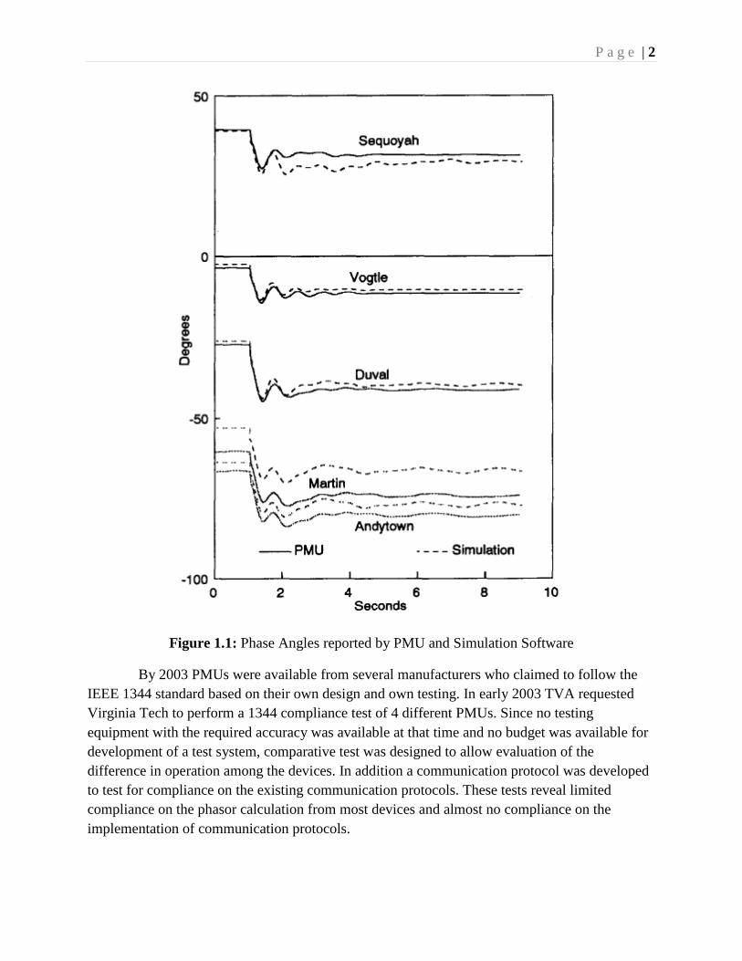
under low load conditions. Figure 1.1 [14] shows the results of one of the line opening
procedures. These tests served as an evaluation of the performance of PMUs and also as an
evaluation of the system models of Georgia power since the PMUs provided the first
measurement to simulation comparison of a wide system event.
During the early 90‟s PMUs continue to be used in several research projects by various
utilities and new manufacturers started developing their own PMUs. In 1995 the first
Synchrophasor standard, IEEE 1344-1995, was released with the aim of guaranteeing a degree of
PMU data for utilities utilizing devices from different manufacturers. The first standard defined
minimum requirements on phase angle and magnitude in addition to providing a communication
protocol for data exchange with PMUs. The main change between the standard and the existing
devices at the time of release was on the requirement of computation of the phasor based on the
measured frequency and not based on a 60 or 50 Hz fundamental frequency.
P a g e | 2
Figure 1.1: Phase Angles reported by PMU and Simulation Software
By 2003 PMUs were available from several manufacturers who claimed to follow the
IEEE 1344 standard based on their own design and own testing. In early 2003 TVA requested
Virginia Tech to perform a 1344 compliance test of 4 different PMUs. Since no testing
equipment with the required accuracy was available at that time and no budget was available for
development of a test system, comparative test was designed to allow evaluation of the
difference in operation among the devices. In addition a communication protocol was developed
to test for compliance on the existing communication protocols. These tests reveal limited
compliance on the phasor calculation from most devices and almost no compliance on the
implementation of communication protocols.

P a g e | 3
After the 2003 blackout the PMUs installed in the Eastern interconnection became key
devices in helping the investigating team put together the sequence of events that explained the
causes of the blackouts. One of the recommendations of the final report of the 2003 blackout was
for the installation of more phasor measurement units [15]. As a result of this recommendation
and the interest of the DOE to encourage the installation of these devices the Eastern
Interconnect Phasor Project, EIPP, was created in 2004. The EIPP was merged with the
collective efforts of the West coast to form the North American SynchroPhasor Initiative in
2007.
With the development and deployment of PMUs in significant numbers, the need for
testing devices gained importance. A set of conformance and performance test procedures are
proposed in the IEEE C37.118 standard aimed to help users assure consistent PMU performance
and to support interoperability of the PMUs. The need for PMU testing is emphasized by the
points [2] listed below.
There are currently a number of companies manufacturing PMUs .PMU hardware from
different manufacturers is likely to be implemented differently, potentially resulting in
inconsistencies and various levels of phasor quality.
Different windowing lengths for computing the phasor, conversion algorithms, filter
characteristics; measurement rate and device resolution can affect the performance of the
PMU.
The PMU performance would be different during normal operation and during faults.
Testing of PMUs could also help understand the source of error, choose the correct
settings for accurate performance and any unseen errors in the algorithm used in the
PMUs.
The delays/latencies caused by the PMUs should be as minimal as possible as this could
cause problems for the phasor data concentrator or other intelligent devices which take
PMU data as input and make control decisions.
Performance characterization can help the utilities (or users) choose the device that best
meets the application needs.
Due to these needs and in coordination with the DOE the National Institute of
Standards and Technology began the development of the Synchrometrology lab [16] in close
collaboration with the Performance and Standard Task team of EIPP (later known as NASPI).
The aim of the Synchrometrology lab was to ensure the interoperability of PMUs by developing
test equipment and test procedures needed to evaluate PMU static and dynamic performance
requirements and communication interface according to the IEEE C37.118 standard.
NIST performed the first PMU evaluation in a group of PMUs provided by ONS, the
Brazilian ISO. ONS is in the process of developing their National Synchrophasor Project and one
P a g e | 4
of their first tasks was to determine the list of PMUs that could be used by the Brazilian utilities
in their implementation. Lack of testing facilities in Brazil led ONS to contact NIST to test their
PMUs in the NIST PMU testing system (described in chapter 2).
1.2. Objective
The aim of NIST Synchrometrology lab was to develop equipment and test procedures
but not to become a testing lab for PMUs. NIST has reached out to universities and other
institutions to utilize their development for creating their own testing facilities. With the funding
of PJM and the support of NIST, Virginia Tech started developing its PMU testing system in
December of 2010. The hardware used in the Virginia Tech system is different from the one used
at NIST due to new hardware upgrades and limited budget of the Virginia Tech project. These
hardware differences and the required changes are part of a previous work [6]. The hardware
differences forced significant software changes in the original PMU testing Software developed
by NIST. This thesis presents the modification and developments performed at Virginia Tech to
successfully develop a PMU testing system based on the original NIST development. The
document also presents some of the results obtained and additional information derived from
those results.
1.3. Thesis Outline
This thesis is organized in the following chapters:
Chapter 2 gives an overview of the IEEE C37.118 standard and various attempts that
have been made for testing the Phasor Measurement Units before and after the release of the
IEEE C37.118 standard. A brief description of the National Institute of Standards and
Technology Steady State PMU Test System and few of the results obtained when a PMU was
tested using the NIST PMU system are illustrated and discussed.
Chapter 3 describes the design of the Virginia Tech Steady State PMU Test System. The
differences between the NIST and VT Test Systems have been highlighted and various issues
that emerged as a result of these differences and the hardware incompatibilities are discussed. A
detailed description of how these issues were solved and the design steps implemented to build a
Virginia Tech Steady State PMU Test System are presented.
Chapter 4 describes the Calibration aspect of the Virginia Tech Steady State PMU Test
System. The various steps that were taken and implemented to correct and compensate for any
possible errors are discussed.

P a g e | 5
Chapter 5 discusses the results obtained when 4 PMUs from different manufactures were
tested for steady state performance using the Virginia Tech Steady State PMU Test System.
Various other issues observed during the testing are also analyzed and presented.
Chapter 6 summarizes the work done, along with the major contributions that this work
made for the Development of a Steady State Test System for PMUs at Virginia Tech. A brief
recommendation of prospective future work is also included.
P a g e | 6
Chapter 2. PMU Testing Prior Development
The IEEE C37.118 Synchrophasor standard [1] was released in 2005 to replace the
obsolete IEEE 1344-1995 standard and to provide better steady state test conditions and
requirements to assess the performance of a Phasor Measurement Unit. This chapter focuses on
the requirements of the IEEE C37.118 standard and reviews previous work aimed to test Phasor
Measurement Units for compliance to this standard.
2.1. The IEEE C37.118 Standard
2.1.1. History of the IEEE C37.118 Standard
The first Synchrophasor standard, IEEE 1344-1995, was released in December of 1995.
This standard defined a message format for data transfer consisting of a header, data, and
configuration frames in addition to command frames to be received by the PMU.A convention
for phasor representation was also defined and synchronization of data sampling was addressed
[7].Specifications for accuracy, response time and process for phasor computing were not
defined.
In May of 2003 tests were performed on Virginia Tech to compare the performance of
4 PMUs from different manufacturers and determine their compliance with the communication
requirements of the IEEE 1344-1995 Standard. The tests fed common voltage and current signals
to all PMUs and compared the angles and magnitudes of the four units under the conditions
defined in the IEEE 1344 Standard. Figures 2.1 and 2.2 show some of the results of these tests.
Figure 2.1 [12] shows the results obtained when the four PMUs were subjected to various
voltage magnitude test signals. The error in Figure 2.1 is computed as a percentage of the
average magnitude of the four PMUs and additional RMS digital multi-meters used during the
test. Figure 2.2 [12] shows the phase angle error of the 4 PMUs in degrees using the average
phase angle as reference.
The results of the comparative tests performed in 2003 revealed a comparable
performance of some of the units and very little adherence by most units to the IEEE 1344
Standard. These tests also revealed that the four units fail to fully comply with the
communication protocols as defined by the IEEE 1344 standard.

P a g e | 7
Figure 2.1: Magnitude Error at nominal frequency [12]
Figure 2.2: Phase shift with respect to the average phase at nominal frequency [12]
The IEEE C37.118 standard was released in December 2005.It addresses the definition
of a synchronized phasor, time synchronization, application of time tags, methods to verify
measurement compliance with the standard, and message formats for communication with a
Phasor Measurement Unit [1]. The timestamp was redefined to consist of three parts, count for
Phase Shift With Respect to the Average
Phase Angle
-0.1500
-0.1000
-0.0500
0.0000
0.0500
0.1000
0.1500
10%
20%
30%
40%
50%
60%
70%
80%
90%
100%
110%
120%
voltage %
deg
rees
PMU A
PMU B
PMU C
PMU D

P a g e | 8
Second of Century (SOC), fraction of a second and status bit for indicating time quality. The
standard however focuses on the steady state performance requirements for a Phasor
Measurement Unit with only recommendations for dynamic performance testing. A new standard
due out in the near future is expected to include the transient performance requirements. The
steady state test requirements are also expected to undergo minor changes.
2.1.2. Synchrophasor definition and Total Vector Error
By definition a phasor is a representation of a sinusoidal signal at a given or common
frequency. Under this definition a sinusoidal signal x(t) = Xmcos(ωt+φ) is said to have a phasor
representation of X = (Xm/√2)(ejφ
) at its given or known frequency. For this phasor the phase
angle, φ, of the sinusoidal signal is referenced to the starting time of the sinusoidal signal and
Xm/sqrt(2) is the RMS magnitude of the sinusoidal signal [1].
A sinusoidal signal as shown in Figure 2.3 is used to obtain a set of phasors
{X0,X1,X2,……..} defined for the intervals {0,T0,2T0,………..}[1].The beginning of each
interval is taken as time reference for the computing the respective phasor.
When a phasor is computed over a period T0, equal to the sinusoidal period T, a constant
phasor is obtained for each observation. If the observed period is different than the period T the
resultant phasors have a constant magnitude with a phase angle that rotates uniformly at the rate
of 2π(f-f0)T0 where f=1/T0 [1].
Figure 2.3: Phasor Computation from samples
[IEEE C37.118-2005 Standard for Synchrophasors for PowerSystems, 2006]. Illustrated under
“Fair Use” copyright guidelines.]

P a g e | 9
The IEEE C37.118 -2005 standard defined and introduced the concept of Total Vector
Error (TVE) to determine the accuracy of a computed phasor. Figure 2.4 illustrates the
relationship between the input signal and the PMU output used by the standard to define the
TVE. The phasor representation of the actual input signal X(t) = Xr(t) + jXi(t) is given by
X = Xr + jXi at any instant of time. The PMU then computes its own phasor from the input signal
that can be represented as X(n) = Xr(n) + jXi(n). The Total Vector Error is then defined as the
vector difference between the phasor of the exact applied signal and the estimated phasor of the
PMU [1].
Figure 2.4: Computation of Total Vector Error
[IEEE C37.118-2005 Standard for Synchrophasors for Power Systems, 2006]. Illustrated under
“Fair Use” copyright guidelines.]

P a g e | 10
2.1.3. Steady State Requirements
The IEEE C37.118 standard focuses on the Steady State requirements and defines
compliance levels for a PMU to pass or fail specific tests aimed to determine the steady state
performance of the PMUs under probable system conditions. A series of steady state tests are
defined and the range of input test signals for what the PMU is expected to show satisfactory
performance. For all the steady state tests the standard defines two compliance levels, Level 0
and Level 1. These Levels define the different ranges of the test signals the PMU needs to be
tested. Both levels require a TVE <1% for a device (PMU) to pass the test and be considered
accurate.
The Steady State Tests required by the standard are:
• Frequency variation
• Magnitude variation
• Phase angle variation
• Harmonic Interference
• Inter-Harmonic Interference
• Unbalanced Magnitude
• Phase Unbalance

P a g e | 11
Table 2.1: Steady State Test Requirements
[IEEE C37.118-2005 Standard for Synchrophasors for Power Systems, 2006]. Illustrated under
“Fair Use” copyright guidelines.]
Table 2.1 defines the various input test signals over which the PMU has to perform. The
compliance levels, Level 0 and Level 1 define the range over which these test signals have to be
varied.

P a g e | 12
2.2. NIST Equipment
The National Institute of Standards and Technology has been very instrumental in
developing a calibrated PMU test system in compliance with the IEEE C37.118-2005 standard.
2.2.1. NIST Steady State Test Set-up
The Steady State Test Set-up used for testing a Phasor Measurement Unit at NIST is
illustrated in Figure 2.5. The PMU being tested is defined as Device Under Test (DUT). The
system is synchronized to UTC via a Global Positioning System (GPS) clock and the
Synchronized three-phase power signals are given as inputs to the DUT. The PMU outputs a
IEEE C37.118 standard formatted continuous data stream at rates up to 60 frames per second.
These data frames contain the time stamped phasor information needed from the DUT. A three-
phase power simulator generates the voltage and current signals to the DUT. The test system has
a control unit which consists of a NIST developed base code implemented in LabView which
performs the data acquisition, phasor computation and processing of the phasor data. The
software controls a six channel sampling system (National instrument supplied Analog Input
Card) that samples the voltage and current waveforms supplied to the PMU using calibrated
resistive attenuators and current transformers (CTs). A 1 PPS serves as the trigger and reference
for defining the phase angles of the test signals.
Figure 2.5: NIST Steady State Test System. [Stenbakken, 2007]. Illustrated under “Fair
Use” copyright guidelines.

P a g e | 13
2.2.2. NIST Steady State Hardware Description
Table 2.2 indicates the various hardware components used by the NIST Test System.
These components are installed in a NI PXI-1042 chassis capable of accepting an external 10
MHz signal to synchronize the backplane system clock. The GPS synchronized 10 MHz
external signal is fed by the SYMETRICOM xLI GPS clock. The Rotek 8100 Signal Generator
provides the necessary 3 phase test signals to perform the steady state tests as described in the
Table 2.1.The Data Acquisition is performed by the Analog Input Card that uses 6(out of 8
available) channels to sense the test voltage and current signals via attenuators and shunts as
illustrated in Figure 2.5.The 1 PPS signal required for triggering and referencing the phase angles
of the test signals is also generated by SYMETRICOM xLI GPS clock.
Table 2.2: NIST Hardware Components
Backplane
Synchronization Source
SYMETRICOM xLI GPS
3 Phase Signal
Generator
Rotek 8100 Signal Generator
Data Acquisition Card NI PXI-6123 - 8 channel analog input 16-bit 500 kS/s/channel
Processor NI PXI-8196 2.0Ghz Pentium M PXI Embedded Controller, Win XP
1 PPS SYMETRICOM xLI GPS
2.2.3. NIST Steady State Software Functionality
All NIST software was implemented on a LabView platform running on a Windows
XP operating system. The NIST software was compatible with the NIST hardware described in
section 2.2.1.This software and hardware combination is capable of performing the steady state
tests(section 2.1.3) required by the IEEE C37.118-2005 standard.
Figure 2.6 illustrates an overview of the software design used for NIST Steady State
PMU Test System. This software automates all the testing procedure as per the user defined
inputs and saves the data and reports generated for future analysis. The signal generation task is
performed by a Rotek Signal Generator which is controlled by the Signal Parameter information
to Rotek block. This block defines the frequency, magnitude, phase angle and harmonic content
information of the test signal. The Rotek Signal Generator starts to execute as soon as it receives
these commands from the Signal Parameter information to Rotek block. The 3 Phase signals thus
generated are fed to the DUT and also sensed by the Analog Input Card via shunts and
attenuators. The DUT phasors are acquired and loaded into the DUT global variables by the
DUT Data Capture block as shown in the figure below. The samples sensed by the Data

P a g e | 14
Acquisition block (using Analog Input Card ) is fed to the NIST Phasor Computation block. A
Fast Fourier Transform (FFT) is performed on these input samples and a Phasor (NIST Phasor)
is computed. These NIST phasors are time stamped and transferred to the comparison block. The
software compares the NIST Phasors and the DUT Phasors based on their timestamps and
computes the corresponding Total Vector Error (TVE).The computed TVE is saved and a report
is generated which can be decoded for further analysis. The test signal is kept in steady state and
tested for a user defined amount of time.
The IEEE C37.118-2005 standard requires that the DUT be tested over a range of
steady state signals as defined in Table 2.1.For a frequency variation test (Level 1) the DUT
needs to be tested for steady state signals in the range of 55Hz to 65Hz. A user first defines the
start frequency, end frequency, step frequency and the duration for which each step needs to be
tested, i.e. the 55 Hz to 65 Hz range is broken into multiple steps (say .1 Hz) and each step is run
for a particular user defined time. The entire process is automated by using a for loop as shown
in Figure 2.6.The start frequency(55 Hz), stop frequency(65 Hz ) and step frequency(.1Hz ) are
defined in the Signal Information Block. The loop runs from 55 Hz to 65 Hz in steps of .1 Hz
and the results obtained for all these steps are saved using Data Saving and Report Generation
block. The various steady state tests required by the standard can be performed by varying the
input parameters defined in the Signal Information block (frequency, phase angle, magnitude and
harmonic content).

P a g e | 15
Figure 2.6: NIST Software Design
Data Saving
and
Report
Generation
via
Ethernet
Data Acquisition
(Analog Input
Card)
DUT
Data Capture
(Write DUT Global
Variables)
Read DUT Global
Variables NIST Phasor
Computation
Signal Parameter
Information to
Rotek
Timestamp based
Comparison of NIST
and DUT Phasors
Timestamp
Generation
Time stamped
NIST Phasors
Signal
Information
Sampling
Information
For Loop

P a g e | 16
2.3. NIST PMU Steady State Test Results
This section describes some of the procedures and results that were obtained when a
DUT was tested by the NIST system. The DUT was tested by NIST for Operador Nacional do
Sistema Elétrico (ONS), the ISO of Brasil [13]. Only a few of the steady state test results
obtained from the ONS PMU Certification Test Report are discussed here.
The following were the steady state tests that were performed as listed in Table 2.1:
Frequency Variation Test
Magnitude Variation Test
Phase Variation Test
Harmonic Distortion Test
Inter-Harmonic Test
The tests discussed were performed in accordance with the Level 1(Table 2.1)
compliance requirement. The device would fail or pass the test if the Total Vector Error was less
than 1% within the range of test signals defined by the Level 1 compliance.

P a g e | 17
2.3.1. Frequency Variation Test
2.3.1.1. Test Description
The frequency of the voltage and current signals is varied from 55 Hz to 65 Hz in steps
of .05 Hz. The magnitude of these signals is maintained at a nominal reference value with the
injected harmonics and the out of band interference are both within the specified limits of less
than 0.2%. Each step is run for 10 seconds and the TVE% statistics (mean, maximum and
median) are obtained from the number of phasors compared during this period.
2.3.1.2. Test Results
The DUT is tested and analyzed for Level 1 as defined in Table 3 of the IEEE C37.118-
2005 standard [1] with a requirement of TVE<1% within ± 5 Hz for Level 1. Figure 2.7 shows
results obtained for the voltage channels at 60 frames/sec.
The DUT passes this test under Level 1 steady state performance requirement.
Figure 2.7: Frequency Variation Test for voltage at 60 frames/second
56 58 60 62 64 66 0
0.1
0.2
0.3
0.4
0.5
0.6
0.7
0.8
0.9
1
Frequency [Hz]
V1 TVE [%]
DUT; Frames per second 60
Mean Max Min

P a g e | 18
2.3.2. Magnitude Variation Test
2.3.2.1. Test Description
For this test the magnitude of the voltage and current signals is varied from 10% to
120% of the nominal voltage in steps of 5% of the nominal. The frequency of these signals is
maintained at a reference value (60 Hz) with the injected harmonics and the out of band
interference both within the specified limits of less than 0.2%. Each step is run for 10 seconds
and the TVE% statistics (mean, maximum and median) are obtained from the number of phasors
compared during this period.
2.3.2.2. Test Results
The DUT is tested and analyzed for Level 1 as defined in Table 3 of the IEEE C37.118-
2005 standard [1] with TVE<1% within 10% to 120% of nominal for Level 1. Figure 2.8 shows
the results obtained for the voltage channels at 60 frames/sec. The DUT passes this test under
Level 1 steady state performance requirement.
Figure 2.8: Magnitude Variation Test for voltage at 60 frames/second
10 20 30 40 50 60 70 80 90 100 110 120 0
0.1
0.2
0.3
0.4
0.5
0.6
0.7
0.8
0.9
1
Magnitude [%]
V1 TVE [%]
DUT; Frames per second 60
Mean Max Min

P a g e | 19
2.3.3. Phase Angle Variation Test
2.3.3.1. Test Description
For this test the phase angle of the voltage and current signals is varied from -180 to
+180 degrees in steps of 1 degree. The magnitude and frequency of these signals is maintained at
a nominal reference value. Each step is run for 34 seconds and the TVE% statistics (mean,
maximum and median) are obtained from the number of phasors compared during this period.
2.3.3.2. Test Results
The DUT is tested and analyzed for Level 1 as defined in Table 3 of the IEEE
C37.118-2005 standard [1] with TVE<1% within ± 180 degrees for Level 1. Figure 2.9 shows
the results obtained for voltage channels at 60 frames/sec. The DUT passes this test under Level
1 steady state performance requirement.
Figure 2.9: Phase Angle Variation Test for voltage at 60 frames/second
-150 -100 -50 0 50 100 150 0.225
0.23
0.235
0.24
Phase [Deg]
V1 Phase Error [Deg]
DUT; Frames per second 60
Phase Error

P a g e | 20
2.3.4. Harmonic Distortion Test
2.3.4.1. Test Description
The test follows Table 3 defined in the IEEE C37.118-2005 standard [1]. A 10%
harmonic is added to the Voltage and Current signals .The steps run from 2nd
harmonic to the
50th
harmonic .The base signal (reference signal) is maintained at 100% nominal value for
voltages and currents at a 60 Hz frequency. Each step is run for 10 seconds and the TVE%
statistics (mean, maximum and median) are obtained from the number of phasors compared
during this period. The injected out of band interference is maintained within 0.2% of the
nominal magnitude.
2.3.4.2 Test Results
The DUT is tested and analyzed for Level 1 as defined in Table 3 of the IEEE C37.118-
2005 standard [1] with TVE<1% at 10% (of nominal magnitude) harmonic for Level 1. Figure
2.10 shows the results obtained for the voltage channels at 60 frames/sec for harmonic distortion
test where the DUT passes the test for Level 1 steady state performance requirement.
Figure 2.10: Harmonic Test for voltage at 60 frames/second
5 10 15 20 25 30 35 40 45 50 0
0.1
0.2
0.3
0.4
0.5
0.6
0.7
0.8
0.9
1
Harmonic Number
V1 TVE [%]
DUT; Frames per second 60
Mean Max Min

P a g e | 21
2.3.5. Inter-Harmonic Test
2.3.5.1. Test Description
The test follows Table 3 defined in the IEEE C37.118-2005 standard [1]. A 10% Inter-
Harmonic is added to the Voltage and Current signals. The steps run for an inter-harmonic
frequency band of 0 to 130 Hz. The base signal (reference signal) is maintained at 100% nominal
value for voltages and currents at a 60 Hz frequency. Each step is run for 10 seconds and the
TVE% statistics (mean, maximum and median) are obtained from the number of phasors
compared during this period. The injected harmonics are maintained within 0.2% of the nominal
magnitude. For 30 frames/sec the frequency band requirement is 45 Hz to 75 Hz and for 60
frames/sec the frequency band is 30 Hz to 90 Hz.
2.3.5.2. Test Results
The DUT is tested and analyzed for Level 1 as defined in Table 3 of the IEEE
C37.118-2005 standard [1] with TVE<1% at 10% nominal magnitude(outside the 30 -90 Hz)
inter-harmonic for Level 1. Figure 2.11 shows the results obtained for the voltage channels at 60
frames/sec. For this result the DUT passes the Level 1 steady state performance requirement.
Figure 2.11: Inter-Harmonic Test for voltage at 60 frames/second
20 30 40 50 60 70 80 90 100 110 120 130 0
0.1
0.2
0.3
0.4
0.5
0.6
0.7
0.8
0.9
1
Inter-Harmonic Frequency [Hz]
V1 TVE [%]
DUT; Frames per second 60
Mean Max Min
P a g e | 22
2.3.6. NIST Test Results
The Devices were tested at NIST as per the requirements of the present IEEE C37.118
standard. Most devices passed the tests except for the out band frequency interference (Inter-
harmonic) test that was failed by all PMUs. These results have helped re-shape the requirements
of the out of frequency interference test for the expected new Synchrophasor standard.

P a g e | 23
Chapter 3. Virginia Tech Steady State PMU Test System
This chapter describes the hardware and software developments required for the
implementation of the Virginia Tech Steady State Phasor Measurement Unit Test System. The
aim of this project was to build a test system at Virginia Tech similar to the test system
developed at the National Institute of Standards and Technology (NIST) with a better or similar
performance compared to that of the NIST test system.
This chapter explains how the Virginia Tech Steady State PMU Test System was
developed by making modifications to the NIST Steady State PMU Test System. An attempt is
made to indicate the main differences between the hardware used in the two systems and the
software compatibility issues that surfaced due to the hardware differences. This chapter also
explains the changes that were made to the initial NIST software to build a fully functional and
flexible Virginia Tech Steady State PMU Test System.
3.1. Initial Developments
The main operational different between the NIST and Virginia Tech systems is on the
three phase signal generation. The NIST system uses an expensive Rotek three phase signal
Generator to produce the various test signals required for steady state testing of PMUs. Budget
limitations required that the Virginia Tech System generate its own signal and use a less
expensive Omicron CMS 156 three phase signal amplifier to obtain the voltage and current
levels required by the PMUs. This change required the development of an independent signal
generation block in LabView capable of generating low level three phase voltage and current
signals which would serve as inputs to the 3 phase amplifier. The amplifier function is to amplify
these signals (20 times) and provide the necessary nominal voltage and current test signals for
the DUT. The amplified signals fed to the DUT are also sensed by the Analog Input Card via
shunts and attenuators to provide samples to the phasor computation block developed by NIST
(as shown in Figure 2.6).
These hardware changes resulted in four important differences between the systems:
a) A three phase signal generation block was required. Fortunately NIST provided an
independent signal generation block, from a different system development, capable of
generating 3 phase signals of various frequencies but due to the lack of a 1PPS reference
the phase angle of the generating signal was not controllable.
b) The other main issue was the inability of the Analog Input Card of the VT system to
synchronize its own base clock with that of the back plane clock of the system. The back
plane of the VT system was designed to be synchronized to an external 10 MHz GPS

P a g e | 24
Synchronized signal and it was expected, in the original design, that the base clock of the
Analog Input Card would synchronize with the back plane clock to emulate the operation
of the NIST system. Lack of synchronization of the input card would cause the test
signals to drift with respect to the 1 PPS signal generated by a NI PXI 6682 H card.
c) The independent signal generation block available from NIST was not capable of
generating interference signals (harmonics and inter-harmonics) as needed to test some of
the requirements of the C37.118 system..
d) A new functionality to the existing DUT Data Capture block obtained from NIST
(Figure 2.6) was needed to develop a function capable of testing the latency of the data
frames.
This chapter describes the hardware components of the VT system and discusses how the
four main issues were solved by accomplishing the following tasks:
Synchronization of the Analog Output and Input cards base clocks to the external GPS
synchronized 10 MHz backplane clock.
Developing of a fully Controllable Signal Generation Block capable of generating 3
phase synchronized signal generation. This block provides the desired phase angle
control and is capable of generating interference signals (harmonic and inter-harmonics).
Integration of the Signal Generation Block into the existing NIST software to automate
and perform real time data acquisition and data generation (signal generation) at the same
time, triggered by a 1 PPS signal.
Developing and implementing a system to compute the latency of the data frames.
The system developed at Virginia Tech required a calibration to compensate for any
possible delays and scaling factor errors that is explained in chapter 4.
3.1.1. VT Steady State PMU Test System Hardware
The VT Test system uses a National Instruments platform for developing a PMU test
system. The tests were developed in LabView 2009 software running on a Windows 7 operating
system. The National Instruments (NI) hardware that was used for VT test system was an
upgraded version to the NI hardware used at NIST and was intended to have a better
performance.
The Hardware used for the VT PMU test system consists of the following key
components.
1) NI Chassis
2) NI Embedded Controller
3) NI Analog Output Card

P a g e | 25
4) NI Analog Input Card
5) NI GPS Time stamping Card
6) Arbiter Clock Synchronized with GPS
7) Three Phase Power Amplifier
8) Attenuators and Shunts
9) Device under Test (DUT, the test PMU)
3.1.1.1. NI Chassis
The NI PXIe 1062Q is a rack mountable 8 slot chassis which holds the controller,
Analog Input/Output cards and the Time stamping card. Its PXI express back plane can be
synchronized to an external 10 MHz clock. This chassis holds the main components (Analog
Input, Output and Time stamping card) of the VT Testing system.
3.1.1.2. NI Embedded Controller
The NI PXIe 8108 is a high performance 2.53 GHz Intel Core 2 Duo T9400
embedded controller and serves as a local workstation to run the LabView 2009 software on a
Windows 7 operating system. The Embedded controller is the main processor for the testing
system and performs all the computations required for signal generation, data acquisition and
data analysis.
3.1.1.3. NI Analog Output Card
The NI PXIe 6733 is an Analog Output card capable of generating 8 output signals.
It has a resolution of 16 bits with a maximum sampling rate of 1MS/s. For the VT PMU test
system only 6 channels are used which serve as the three phase voltage and current inputs to the
three phase power amplifier. The analog channels are drawn out through the SCB 68 pin-out
device before being fed to the amplifier. The SCB provides easy access to the pins of the Analog
Output Card.
3.1.1.4. NI Analog Input Card
The NI PXIe 6356 is a Data Acquisition Card (DAQ) capable of reading up to 8
Analog voltage signals. It has a resolution of16 bits with a maximum sample update capability of
1.25 MS/s. Similar to the Analog Output card, the analog input signals are interfaced with the NI
PXIe 6356 through another SCB 68 pin-out device. This card enables the VT test system to
sample and digitize the analog signals that the three phase amplifier feeds to the DUT.

P a g e | 26
3.1.1.5. NI GPS Time stamping Card
The NI PXI 6682 H card serves as a timing module for the Virginia Tech Test
System. This module is connected to an antenna to acquire the GPS signals. With the help of NI
Sync drivers (software drivers for 6682 H card), precise timestamps as well as I PPS signals may
be generated.
3.1.1.6. Arbiter Clock Synchronized with GPS
The external 10 MHz clock required for NI backplane synchronization is obtained
from the 10 MHz output port of an Arbiter 1084B Clock. The Arbiter clock requires an antenna
with a receiver to acquire the GPS signals.
3.1.1.7. Three Phase Power Amplifier
An OMICRON CMS 156 amplifier magnifies the 3 phase low level voltage signals
generated by the testing system Analog Output Card to the nominal voltages and currents
required by the DUT. In most cases the voltages and currents are amplified by a factor of 20
before they are fed to the DUT .This factor is used as one of the input parameter to the blocks
generating the test signal to get the desired amplitude.
3.1.1.8. Device Under Test (the test PMU)
The Device Under Test, DUT is the PMU which is being tested. It should be capable
of generating Data frames, Configuration and Command frames as defined by IEEE C37.118
format. Also it should use either TCP or UDP communication format to send/receive the frames.
3.1.2. Hardware Differences between NIST and VT Test Systems
This section highlights the hardware differences between the NIST and the VT test
systems. The performance of these hardware components is also compared to determine the
performance of the overall system.
The NIST system (Figure 2.5 and 2.6) uses a 1 PPS synchronized 3 phase Rotek signal
generator to generate the test signals whereas the NIST system uses an amplifier to amplify the
low level signals from the Analog Output Card into high level test signals.

P a g e | 27
The back plane synchronization of the NIST system is obtained using a 10MHz signal
generated by the Symmetricom XLI GPS clock whereas the VT system uses a 10 MHz signal
generated from the Arbiter 1084 B Clock.
The NIST system uses an Intel Pentium M760 processor whereas the VT system uses
an Intel core 2 duo T9400 processor.
The 1 PPS necessary for the NIST system comes from the same Symmetricom XLI
GPS clock used for the 10 MHz signal while the 1PPS for VT system is obtained from NI PXI-
6682 H Card.
The data acquisition card used by NIST is a NI PXI-6123 card capable of capturing up
to 500 KS/s while the NI PXIe-6356 can capture up to 1.25 MS/s.
The Table 3.1 summarizes the hardware differences [6] between the two systems
along with the accuracy/performance of each hardware component. The VT system has a
superior processor, higher capability Analog Input Card and more accurate backplane
synchronization signal whereas the NIST has more precise 1 PPS signal .The Virginia Tech
system has an additional phase error of .000748 degrees for 60 Hz[6].This error is very
negligible when compared to the 1% TVE. The performance and accuracy of the Virginia Tech
System when similar software is used is better or at least same as that of the Virginia Tech
system.
Table 3.1: Hardware components comparison used at NIST and VT
P a g e | 28
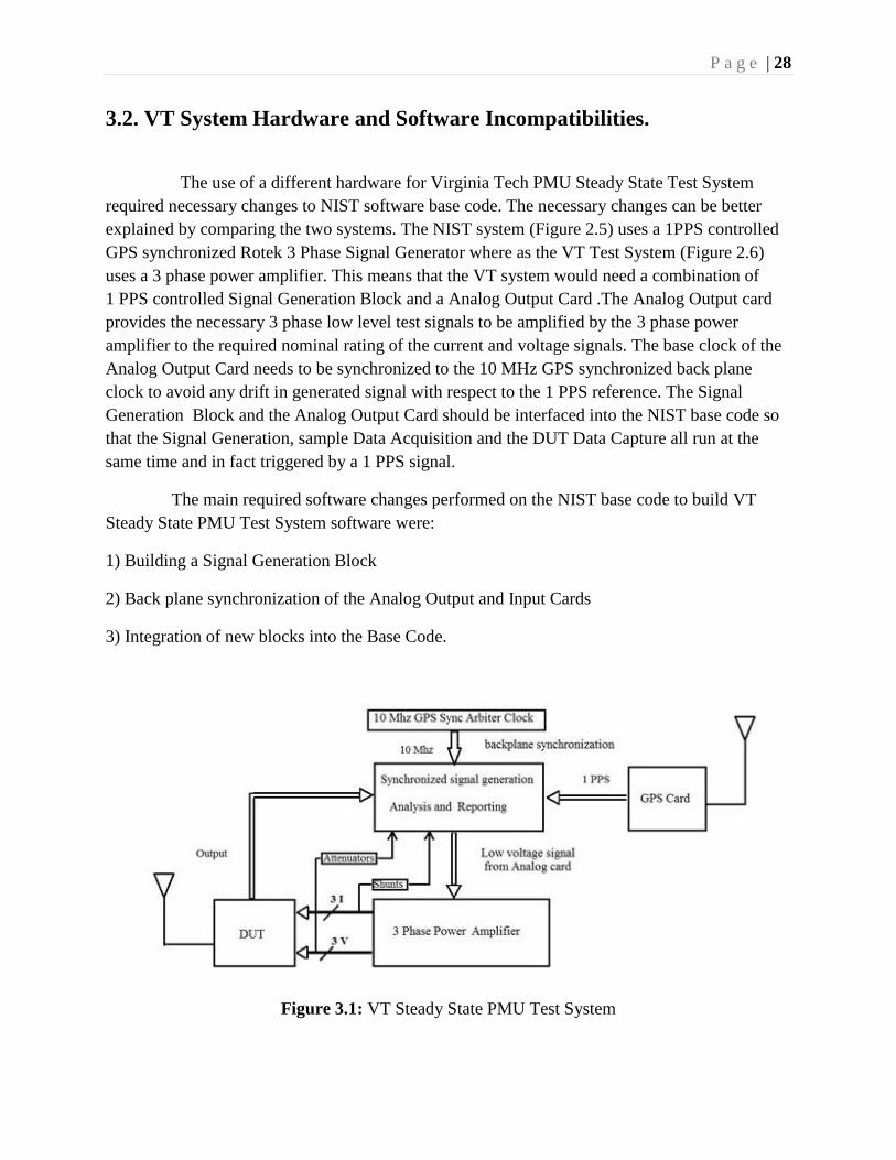
3.2. VT System Hardware and Software Incompatibilities.
The use of a different hardware for Virginia Tech PMU Steady State Test System
required necessary changes to NIST software base code. The necessary changes can be better
explained by comparing the two systems. The NIST system (Figure 2.5) uses a 1PPS controlled
GPS synchronized Rotek 3 Phase Signal Generator where as the VT Test System (Figure 2.6)
uses a 3 phase power amplifier. This means that the VT system would need a combination of
1 PPS controlled Signal Generation Block and a Analog Output Card .The Analog Output card
provides the necessary 3 phase low level test signals to be amplified by the 3 phase power
amplifier to the required nominal rating of the current and voltage signals. The base clock of the
Analog Output Card needs to be synchronized to the 10 MHz GPS synchronized back plane
clock to avoid any drift in generated signal with respect to the 1 PPS reference. The Signal
Generation Block and the Analog Output Card should be interfaced into the NIST base code so
that the Signal Generation, sample Data Acquisition and the DUT Data Capture all run at the
same time and in fact triggered by a 1 PPS signal.
The main required software changes performed on the NIST base code to build VT
Steady State PMU Test System software were:
1) Building a Signal Generation Block
2) Back plane synchronization of the Analog Output and Input Cards
3) Integration of new blocks into the Base Code.
Figure 3.1: VT Steady State PMU Test System

P a g e | 29
The VT Steady State PMU Test system and NIST Test system use a LabView platform
for implementing the software that operates with the hardware components obtained from
National Instruments. LabView is a graphical programming language and all the functionalities
are built using virtual Instrument‟s (vi). A “vi” has two interfaces, a front panel where the user
can enter the desired inputs required for execution of the function and can also view the results
obtained the program. The second interface is the block diagram interface where the
implementation of the program/function is performed. Appendix A provides a listing of the main
block diagram interfaces developed for the Virginia Tech test system.
3.2.1. Building a Signal Generation Block
The VT PMU Steady State Test System should be capable of generating all the test
signals (Table 2.1) as required by the IEEE C37.118 standard [1]. Each steady state test is made
to run by varying the test signal parameters within a defined range (Level 0 and Level 1) .The
test is automated by designing a for loop and incrementing the signal parameter in steps from
starting point to the ending point of the defined range. For a frequency variation test (Level 1)
the test signal is varied from 55 Hz to 65 Hz in steps of .05 Hz, i.e. the loop iterates 200 times
and each step is maintained at steady state for a user defined amount of time (default value of 15
seconds).This section explains how the designed software produces the required signals for the
user defined amount of time.
A memory Block Size is first defined as the number of samples required to be
generated during the testing period. For a defined sampling rate of the Analog Output Card
(default of 50 K samples/sec) and the testing time of the step (15 s) ,the block size is defined as
Block Size= (sampling rate * testing time of step)
For sampling rate =50000 samples/sec, testing time = 15 sec,
Block Size= (50000 samples/sec * 15 sec) =750000 samples.
A Single Phase FM and AM Signal Generation is explained first. A Harmonic
Generation is added and finally a 3 Phase FM, AM and HM Signal Generation is built.

P a g e | 30
3.2.1.1. Single Phase FM and AM Signal Generation
The block size is fed as an input to a ramp function which generates an array with
values from 0 to block size-1([0, 1,2,…………blocksize-1]).Each element in this array is then
divided by the sampling rate of the output card to get the sample time values. With the sampling
rate of the output card defined as fst ,the various sample times are represented by the array
[0/fst,1/fst,2/fst,…………blocksize-1/fst].Using this array of sample times an array (Single Phase
Buffer ) of required samples is generated by using formula (1):
A(1+ma*cos(2*π*fm*t +φa))*cos(2*π*fc*t+mf*sin(2*π*fm*t+ φf)+φ) (1)
(t=i/ fst, for 0≤t ≤ (blocksize-1)/fst)
Where
A= Amplitude of the nominal frequency signal.
fc= Frequency of the nominal frequency signal
φ= Initial phase of the nominal frequency signal.
ma= Amplitude of the amplitude modulating signal.
φa= Initial phase of the amplitude modulating signal.
mf= Amplitude of the frequency modulating signal.
fm=Frequency of the modulating wave.
φf = Initial phase of the frequency modulating signal.
Figure 3.2(Lab View implementation illustrated in Figure A.1 of Appendix A)
illustrates the implementation of equation 1. At first the modulating components, Amplitude
Modulation and Frequency Modulation blocks are implemented as shown in the figure. The
Amplitude modulation block takes fm,, ma, φa and t as input values and generates an output
defined by (1+ma*cos(2*π*fm*t +φa)). Similarly the Frequency Modulation block uses fm , φf, mf
and t as input values to generate an output defined by (mf*sin(2*π*fm*t+ φf)). The outputs of the
Frequency Modulation and the Amplitude Modulation are utilized to modulate the base signal
(nominal signal) to build the final equation 1

P a g e | 31
A(1+ma*cos(2*π*fm*t +φa))*cos(2*π*fc*t+mf*sin(2*π*fm*t+ φf)+φ)
The Single Phase Buffer consists of an array of samples corresponding to the sample
times [0/fst,1/fst,2/fst,…………blocksize-1/fst. The flexibility required to accomplish the testing
requirements of the IEEE C37.118 standard is easily obtained by allowing the user (through
software modules) to change the parameters of equation 1.
Figure 3.2: Single Phase FM and AM Signal Generation
fc
φ
mf
φf
fm
ma
φa
A
Block SizeRamp
Function
Start point
Start point
Div
Sampling
Frequency
[0/fst,1/fst,2/fst,…………blocksize-1/fst]
Array(t)
mf*sin(2*π*fm*t+ φf )
(1+ma*cos(2*π*fm*t +φa)
A(1+ma*cos(2*π*fm*t +φa))*cos(2*π*fc*t+mf*sin(2*π*fm*t+ φf)+φ)
Amplitude
Modulation
Frequency
Modulation
Modulation of
Base Signal
t
Single Phase Buffer

P a g e | 32
3.2.1.2. Single Phase FM, AM and HM Signal Generation
The Single Phase FM and AM Signal Generation can be updated to add an additional
functionality, the Harmonic Signal Generation. The implementation is shown in the
Figure 3.3 (Lab View implementation illustrated in Figure A.2 of Appendix A). The user defines
the amplitude of the harmonic signal (percentage of the nominal magnitude signal) and the
desired harmonic to be generated. The Harmonic Signal block generates an output defined by
((Harmonic %)/100*A*cos(2*π*n*fc*t+φ))
where
Harmonic % = harmonic percentage (of nominal magnitude)
n = harmonic number.
The array generated by the Harmonic Signal block is added to the output array of the
Modulation of base signal block to obtain the final resultant Single Phase Buffer. The resultant
buffer represents the output samples of the Single Phase FM, AM and HM Signal Generation
Block.

P a g e | 33
Figure 3.3: Single Phase FM, AM and HM Signal Generation
fc
φ
mf
φf
fm
ma
φa
A
Block SizeRamp
Function
Start point
Start point
Div
Sampling
Frequency
[0/fst,1/fst,2/fst,…………blocksize-1/fst]
Array(t)
mf*sin(2*π*fm*t+ φf )
(1+ma*cos(2*π*fm*t +φa)
A(1+ma*cos(2*π*fm*t +φa))*cos(2*π*fc*t+mf*sin(2*π*fm*t+ φf)+φ)
Amplitude
Modulation
Frequency
Modulation
Modulation of
Base Signal
t
Single Phase Buffer
(Harmonic %)/100*
Acos(2*π*n*fc*t+φ)
Harmonic Signal
Harmonic % X
Harmonic
Number(n) X

P a g e | 34
3.2.1.3. Three Phase FM, AM and HM Signal Generation
Once the Single Phase FM, AM and HM Signal Generation block is built the 3 Phase
FM, AM and HM Signal Generation is built by modifying the phase angle input parameter of the
Single Phase FM, AM and HM Generation block as shown in Figure 3.4( Lab View
implementation illustrated in Figure A.3 of Appendix A).The Single Phase Generation blocks are
replicated 6 times(3 for voltages and 3 for currents) and a 3 Phase Signal Generation is built.
For a balanced 3 Phase System the phase angles of voltages VA, VB and VC are 0,-120
and +120 degrees respectively. Similarly the phase angles of currents for IA, IB, and IC are 0,-120
and +120 degrees respectively. These angles may be varied if an unbalanced Phase Test is
intended to be performed. The resultant buffer is a 2 dimensional array of 6 single dimensional
arrays (3 for voltages and 3 for currents).
Figure 3.4: Three Phase FM, AM and HM Signal Generation
Signal
Information
3 Phase
Current
Information
Single Phase
Information
VB
Single Phase
Information
VC
Single Phase
Information
VA
3 Phase
Voltage
Information
Single Phase
Information
IB
Single Phase
Information
IC
Single Phase
Information
IA
Single Phase
FM,AM,HM
Generation
Single Phase
FM,AM,HM
Generation
Single Phase
FM,AM,HM
Generation
Single Phase
FM,AM,HM
Generation
Single Phase
FM,AM,HM
Generation
Single Phase
FM,AM,HM
Generation
Buffer
0
-120
+120
-120
+120
0

P a g e | 35
3.2.2. Back plane synchronization of the Analog Output and Input Cards
These arrays (buffers) obtained from 3 Phase FM, AM and HM Signal Generation
block are loaded into the input buffer of the Analog Output Card. Once the Analog Output Card
starts, it samples out the elements in these arrays (3 set of voltages and 3 set of currents) at the
programmed sampling rate (50 K samples/sec) until the end of the buffer is reached. The angles
defined for the voltage and current channels are defined with respect to the 1 PPS. To maintain a
constant desired angle with respect to the 1 PPS the Analog Output Card should start when a 1
PPS occurs and the sampling clock of the Analog Output Card should be synchronized to the
GPS. A synchronized clock is necessary for signal generation to ensure that the output test signal
does not drift with respect to the 1 PPS. An initial attempt was made to synchronize the Analog
Output base clock to the backplane clock (already GPS synchronized) but due to the incapability
of the Analog Output Card to utilize the back plane an alternative approach was followed as
described in Figure 3.6.
The present VT Test System utilizes the 10MHz GPS synchronized signal from Arbiter
1084B GPS clock to synchronize the back plane of the NI device (Figure 35). Whenever a
10 MHz clock is detected on the 10MHz REF IN connector, the backplane automatically phase
locks the PXI_CLK10 and PXIe_CLK100 signals to this external clock and distributes these
signals to the slots attached to the chassis as shown in Figure 3.5.
Figure 3.5: Backplane, PXI_CLK10 and PXI CLK10 and PXIe_CLK100 synchronization
[NI PXIe-1062Q User Manual] Illustrated under “Fair Use” copyright guidelines

P a g e | 36
The Analog Input card has the capability to synchronize its 20 MHz Timebase (base
clock) using the 100 MHz GPS synchronized signal. The DAQmx Timing property node
function (Figure 3.6) performs the task of synchronizing the input card base clock to the 100
MHz signal (PXIe_Clk100) with the help of the Get Terminal block (predefined vi in LabView
2009, used to access the desired signal).
A similar procedure could be repeated for Analog Output card but its inability to use
the PXI_CLK10 or PXIe_CLK100 signals required an alternative procedure of importing the
Time base of the Analog Input card on to the Time base of the Analog Output card as shown in
the Figure 3.6 (Lab View implementation illustrated in Figure A.4 of Appendix A). Instead of
synchronizing the Analog Output card base clock to the back plane, the Analog Output card base
clock was synchronized to the Analog Input Base clock. So the Analog Input card is
synchronized first followed by the Analog Output card. As shown in Figure 3.6 the 20 MHz
synchronized Time base (of Analog Input card) is now imported on to the Analog output card
Master Time base through the DAQmx timing property node function. Once the Analog Input
card is initialized and starts (Input task ),this input task(shown as 1) now triggers the output task
(shown as 2) thus releasing the Output task (Output card tasks).This ensures that both cards are
started at the same time with their respective base clocks synchronized to GPS.
Figure 3.6: Base clock synchronization of Analog Input and Output Cards
Analog Input
Card Channels
Initialization
Analog Ouput
Card Channels
Initialization
Get
Terminal
Get
Terminal
DAQmx Timing
Ref Clk.Src
Ref Clk.Rate
DAQmx Timing
Ref Clk.Src
Ref Clk.Rate
Generate
Trigger
Wait for
Trigger
Sampling
Information
Sampling
Information
100000000
PXIe_Clk100
20000000
1
2

P a g e | 37
3.2.3. Integration of new blocks into the Base Code
The blocks developed in section 3.2.1 and sections 3.2.2 have to be integrated into
NIST software base code to build the software for the Virginia Tech PMU Steady State Test
System. Figure 3.7 illustrates the block diagram implementation of integrating the new
functionalities into the NIST base code. The Signal Generation Block along with the Analog
Output Card provides the necessary low level Inputs to the 3 Phase Power Amplifier. The signal
Sync 1in Figure 3.7 correspond to the PXIe_clk100 , the 100 MHz back plane signal required to
synchronize the base clock of Analog Input Card, whereas Sync 2 is the 20 MHz base clock
signal of the Analog Input card which is used to the synchronize the base clock of the Analog
Output card. As discussed in section 3.2.2 to generate test signals of desired phase angles, (with
respect to 1 PPS) the Analog Output Card should start exactly at the 1 PPS as shown in Figure
3.7. The new software system thus built does not have any compatibility issues with the
hardware used at Virginia Tech.
Figure 3.7: Virginia Tech PMU Steady State Test System Software Design
Data Saving
and
Report
Generation
via
Ethernet
Data Acquisition
(Analog Input
Card)
DUT
Data Capture
(Write DUT Global
Variables)
Read DUT Global
Variables NIST Phasor
Computation
Signal
Generation
Block
Timestamp based
Comparison of NIST
and DUT Phasors
Timestamp
Generation
Time stamped
NIST Phasors
Signal
Information
Sampling
Information
For Loop
Analog Output
Card
CMS 156
3 Phase Power
Amplifier
1 PPS Trigger
100 Mhz GPS Synchronized Back plane signal
Trig TrigTrig
Sync1
Sync 2
P a g e | 38
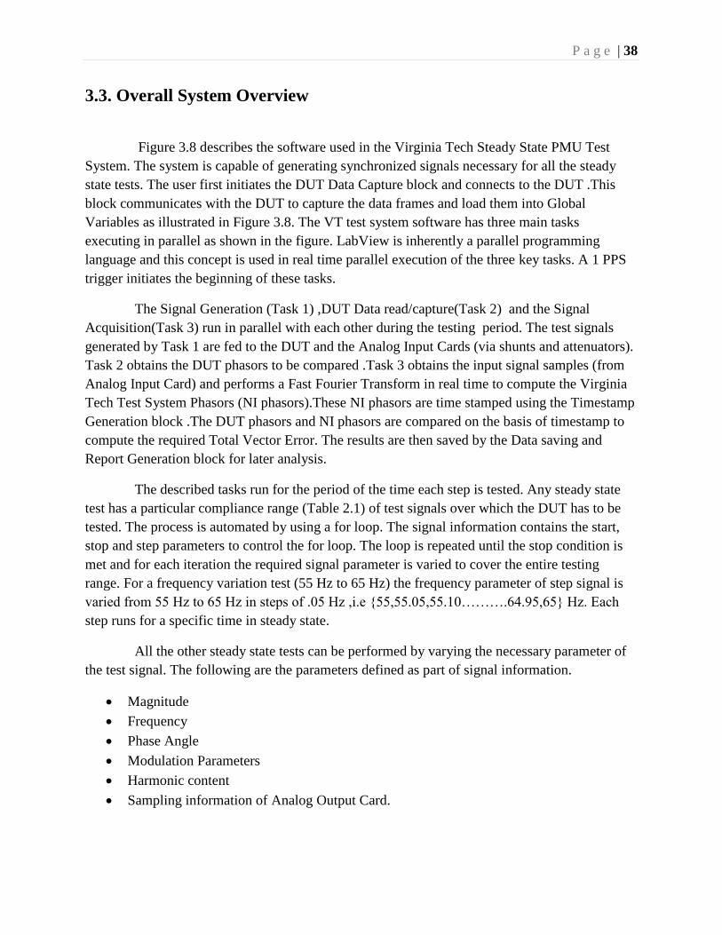
3.3. Overall System Overview
Figure 3.8 describes the software used in the Virginia Tech Steady State PMU Test
System. The system is capable of generating synchronized signals necessary for all the steady
state tests. The user first initiates the DUT Data Capture block and connects to the DUT .This
block communicates with the DUT to capture the data frames and load them into Global
Variables as illustrated in Figure 3.8. The VT test system software has three main tasks
executing in parallel as shown in the figure. LabView is inherently a parallel programming
language and this concept is used in real time parallel execution of the three key tasks. A 1 PPS
trigger initiates the beginning of these tasks.
The Signal Generation (Task 1) ,DUT Data read/capture(Task 2) and the Signal
Acquisition(Task 3) run in parallel with each other during the testing period. The test signals
generated by Task 1 are fed to the DUT and the Analog Input Cards (via shunts and attenuators).
Task 2 obtains the DUT phasors to be compared .Task 3 obtains the input signal samples (from
Analog Input Card) and performs a Fast Fourier Transform in real time to compute the Virginia
Tech Test System Phasors (NI phasors).These NI phasors are time stamped using the Timestamp
Generation block .The DUT phasors and NI phasors are compared on the basis of timestamp to
compute the required Total Vector Error. The results are then saved by the Data saving and
Report Generation block for later analysis.
The described tasks run for the period of the time each step is tested. Any steady state
test has a particular compliance range (Table 2.1) of test signals over which the DUT has to be
tested. The process is automated by using a for loop. The signal information contains the start,
stop and step parameters to control the for loop. The loop is repeated until the stop condition is
met and for each iteration the required signal parameter is varied to cover the entire testing
range. For a frequency variation test (55 Hz to 65 Hz) the frequency parameter of step signal is
varied from 55 Hz to 65 Hz in steps of .05 Hz ,i.e {55,55.05,55.10……….64.95,65} Hz. Each
step runs for a specific time in steady state.
All the other steady state tests can be performed by varying the necessary parameter of
the test signal. The following are the parameters defined as part of signal information.
Magnitude
Frequency
Phase Angle
Modulation Parameters
Harmonic content
Sampling information of Analog Output Card.

P a g e | 39
Figure 3.8: Overview of Virginia Tech PMU Steady State Test System Software
Data Saving
and
Report
Generation
via
Ethernet
Data Acquisition
(Analog Input
Card)
DUT
Data Capture
(Write DUT Global
Variables)
Read DUT Global
Variables NIST Phasor
Computation
Signal
Generation
Block
Timestamp based
Comparison of NIST
and DUT Phasors
Timestamp
Generation
Time stamped
NIST Phasors
Signal
Information
Sampling
Information
For Loop
Analog Output
Card
CMS 156
3 Phase Power
Amplifier
1 PPS Trigger
100 Mhz GPS Synchronized Back plane signal
1 2
3
Trig Trig Trig
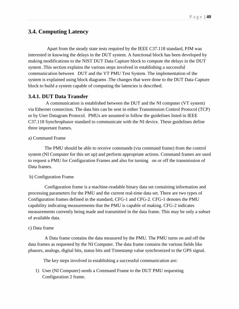
P a g e | 40
3.4. Computing Latency
Apart from the steady state tests required by the IEEE C37.118 standard, PJM was
interested in knowing the delays in the DUT system. A functional block has been developed by
making modifications to the NIST DUT Data Capture block to compute the delays in the DUT
system .This section explains the various steps involved in establishing a successful
communication between DUT and the VT PMU Test System. The implementation of the
system is explained using block diagrams .The changes that were done to the DUT Data Capture
block to build a system capable of computing the latencies is described.
3.4.1. DUT Data Transfer
A communication is established between the DUT and the NI computer (VT system)
via Ethernet connection. The data bits can be sent in either Transmission Control Protocol (TCP)
or by User Datagram Protocol. PMUs are assumed to follow the guidelines listed in IEEE
C37.118 Synchrophasor standard to communicate with the NI device. These guidelines define
three important frames.
a) Command Frame
The PMU should be able to receive commands (via command frame) from the control
system (NI Computer for this set up) and perform appropriate actions. Command frames are used
to request a PMU for Configuration Frames and also for turning on or off the transmission of
Data frames.
b) Configuration Frame
Configuration frame is a machine-readable binary data set containing information and
processing parameters for the PMU and the current real-time data set. There are two types of
Configuration frames defined in the standard, CFG-1 and CFG-2. CFG-1 denotes the PMU
capability indicating measurements that the PMU is capable of making. CFG-2 indicates
measurements currently being made and transmitted in the data frame. This may be only a subset
of available data.
c) Data frame
A Data frame contains the data measured by the PMU. The PMU turns on and off the
data frames as requested by the NI Computer. The data frame contains the various fields like
phasors, analogs, digital bits, status bits and Timestamp value synchronized to the GPS signal.
The key steps involved in establishing a successful communication are:
1) User (NI Computer) sends a Command Frame to the DUT PMU requesting
Configuration 2 frame.
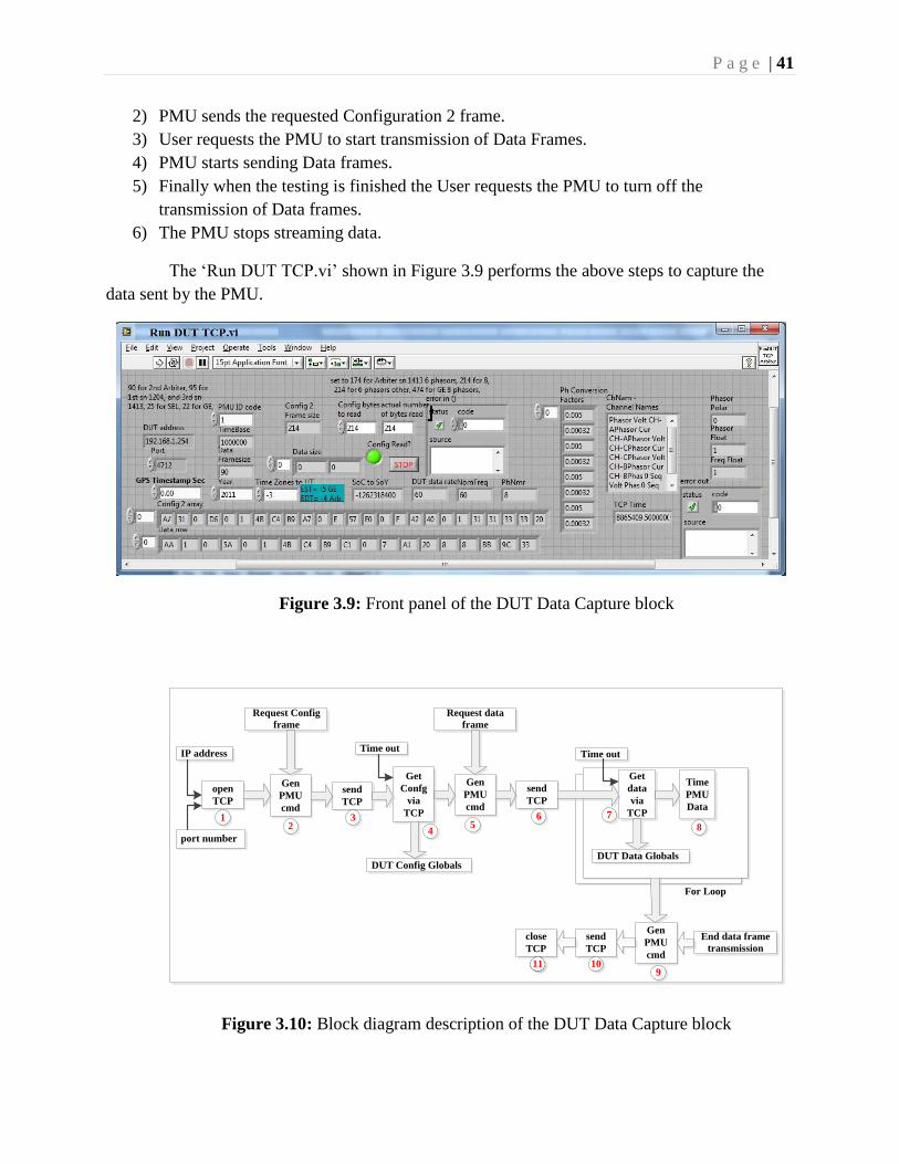
P a g e | 41
2) PMU sends the requested Configuration 2 frame.
3) User requests the PMU to start transmission of Data Frames.
4) PMU starts sending Data frames.
5) Finally when the testing is finished the User requests the PMU to turn off the
transmission of Data frames.
6) The PMU stops streaming data.
The „Run DUT TCP.vi‟ shown in Figure 3.9 performs the above steps to capture the
data sent by the PMU.
Figure 3.9: Front panel of the DUT Data Capture block
Figure 3.10: Block diagram description of the DUT Data Capture block
Gen
PMU
cmd
Request data
frame
send
TCP
open
TCP
IP address
port number
Gen
PMU
cmd
send
TCP
Get
Confg
via
TCP
Request Config
frame
DUT Config Globals
Get
data
via
TCP
Time
PMU
Data
DUT Data Globals
For Loop
Gen
PMU
cmd
End data frame
transmission
send
TCP
close
TCP
12
3
45
6 7
8
91011
Time outTime out
P a g e | 42
Figure 3.10 shows the various sub blocks involved in the design of DUT Data Capture
block. The design and the flow of the logic is as described below. The flow of control follows the
sequence shown in Figure 3.10 from Block 1 to Block 11.
Block 1) This (open TCP) block opens a TCP connection
Block 2) This block (Gen PMU cmd) builds the command frame requesting the DUT for
Configuration 2 frame
Block 3) The command frame built in block 2 is sent to the DUT using this block (send TCP)
Block 4) This block (Get Confg via TCP) receives the Configuration 2 frame from the DUT. The
array holding the Configuration 2 frame bits is used by the Configuration frame decoder to
obtain the various fields in the Configuration frame and store them as global Variables. These
global variables play a crucial role in sharing the data across different vi‟s(functions) .The data
stored in these global variables can be read/written by any functions(vi blocks) defined inside the
directory. Care is taken when writing into these global variables as the data can get corrupted if
multiple functions try to access(write) into these variables at the same time. In this system design
the global variables associated with the Configuration and Data frames are written only in Run
DUT TCP.vi but can be read by all other functions defined in the directory to ensure the
credibility of the data.
Block 5) Once the Configuration frame is obtained this block (Gen PMU cmd) generates a
command frame requesting the DUT to turn on the transmission of data frames.
Block 6) This block (send TCP) sends the command frame generated by the previous block to
the DUT.
Block 7) This block (Get data via TCP) obtains the data frames sent by the DUT. The data
frames thus obtained are saved as global variables which are used later by the comparator
algorithm .This block has an important input called the timeout value. Timeout value is the time
for which this block can wait for the next data frame to arrive before terminating the connection.
In short, if a data frame is not obtained by this block within this timeout period, measured from
the time when the last frame was captured, the connection would be terminated. A value of 250
ms is being used for this design.
Block 8) This block (Time PMU data) saves and loads the data into the set of global variables
assigned for data frame. Blocks 7 and 8 are inside a continuous loop which stops only when the
user activates the button located on the front panel. Blocks 7 and 8 are made to repeat for each
iteration (data frame) .Generally this loop execution is stopped by the user when the testing
process is over.
Block 9) The command frame requesting the PMU to stop the transmission of data frames is
generated by this block (Gen PMU cmd).

P a g e | 43
Block 10) Once the loop execution ends this block (send TCP) runs automatically and sends the
command frame generated by the previous block to the DUT to stop data frames transmission
Block 11) This is the final step in the process which closes the TCP connection previously
established.
The above eleven blocks form the basis for establishing a TCP connection with DUT
using IEEE C37.118 2005 message format.

P a g e | 44
3.4.2. DUT Data Latency
Figure 3.11(Lab View implementation illustrated in Figure A.5 of Appendix A)
illustrates how the Data Capture block is utilized to compute the latency (delay) between
subsequent data frames. The Generate Time sub block inside the for loop generates a time
whenever a data frame is received by the Get data via TCP block. The Generate Time block
generates a time value making use of the NI Sync drivers which can access the NI PXI 6682 H
card and generate GPS synchronized timestamps. This time generated can be temporarily stored
in shift registers (predefined in LabView) and is made available for the next iteration. Thus the
Time Difference block computes the time difference making use of the time corresponding to
present data frame and the time of previous data frame available through shift register. The
Generate Time block and the Time Difference block run for every iteration and the time
difference (latency) is plotted in real time. The results obtained for various DUT‟s tested are
discussed in chapter 5 under the DUT Latency section.
Figure 3.11: Block diagram showing Latency Computation using DUT Data Capture block
Gen
PMU
cmd
Request data
frame
send
TCP
open
TCP
IP address
port number
Gen
PMU
cmd
send
TCP
Get
Confg
via
TCP
Request Config
frame
DUT Config Globals
Get
data
via
TCP
Time
PMU
Data
DUT Data Globals
For Loop
Gen
PMU
cmd
End data frame
transmission
send
TCP
close
TCP
12
3
45
6 7
8
91011
Time out
Time out
Generate
TimeTime
Difference
X
X
X = Shift Register

P a g e | 45
Chapter 4. Test System Calibration
The VT Steady State Test System is used to test the PMUs for their steady state
performance following the guidelines in the IEEE C37.118-2005 standard. The standard requires
the test systems to have a test accuracy ratio of at least four times that of the test requirements,
i.e. for a test requirement of 1% TVE the test equipment should have a TVE accuracy of at least
.25%. In general a test system is recommended to have one tenth the tolerance of the test
requirement [6]. The NIST PMU Calibration System has been calibrated to have less than
0.015% maximum magnitude uncertainty, and less than 0.009 degree maximum angle
uncertainty (less than 0.4 microsecond time uncertainty),which means the test system has an
uncertainty of less than 0.015% TVE[6].
The VT PMU Steady State Test System uses the software obtained from NIST with
several modifications to make the software compatible with the different hardware selected for
the test system (as explained in Chapter 3).The hardware used for building the Virginia Tech
Test System has a better or similar accuracy thus ensuring that the performance of the Virginia
Tech PMU Test System can be at least the same as that of the NIST Test System when properly
calibrated.
4.1. Test System Requirements
The errors in the Test System could be induced from various sources. The following are
the prime non negligible sources of error. The net contribution of all the errors should be within
.25 % TVE for a test system.
Magnitude accuracy
Phase delays
Accuracy of the PPS used in the system
Synchronization accuracy of sampling clocks
4.1.1. Magnitude Accuracy
The phasors are computed by the NI computer (VT PMU Test System) from the
samples acquired by the Analog Input Card. The Analog Input Card is designed to sense low
level signals in the range of -10 to +10 volts. The tests signals have magnitudes much higher
than the values accepted by the Analog Card thus requiring an additional device to step down the
value of these test signals. Shunts are introduced into the system to provide a scaled voltage

P a g e | 46
equivalent of the actual current signals. Attenuators similarly provide the scaled low level
voltage of the actual voltage signals. The phasors thus computed should be finally multiplied by
these scaling factors to obtain the phasor values of the actual test signal. A 1% error on the
magnitude causes a corresponding 1% in the TVE.
The attenuators and shunts have to be accurately calibrated to obtain scaling values
with negligible error. The shunts and attenuators were calibrated using a recently factory
calibrated Agilent 34401A multimeter. The range of the actual test signals vary from 10%-120%
of nominal (70 Volts rms) for voltages and 10%-120% of nominal (5 Amperes rms) for the
currents. The ranges for corresponding scaled values are (350 mv -4.2 v) rms for voltage and
(25mv-300mv) rms for the currents.
4.1.2. Phase Delays
As mentioned before the samples required for phasor computation of actual signal are
sensed via shunts, attenuators, Analog Input Card and the connecting wires. These devices may
cause time delays in sensing the actual signal and are reflected as phase errors in the phasor
computation. These delays have to be accurately calculated and compensated (during phasor
calculation) as a phase error of 1 degree (46.29 micro seconds) contributes an error of 1.75%
TVE.
4.1.3. Accuracy of the GPS 1 PPS
The accuracy of the GPS 1 PPS signal is of importance in the system as it serves as a
reference for defining the phase angle of the signal during signal generation .It also serves as a
reference in computing the above mentioned phase delays (section 4.1.2). The 1 PPS generated
by the NI PXI-6682 H card in the Virginia Tech PMU Test System has a phase error of .000748
degrees for 60 Hz[6] contributing a negligible value to the total TVE % error.
4.1.4. Synchronization of sampling clocks
An Arbiter 1084B provides the necessary 10 MHz for backplane synchronization and is
more accurate than the synchronization signal provided for the NIST PMU Test System. The
synchronization of the base clocks used in Analog Input and Output Card‟s is important for the
test system as this defines how accurately the generated and acquired signals are locked to the 1
PPS (GPS) reference. The Virginia Tech Test System has a synchronization error of .001254
degrees (for 60 Hz) which has a negligible contribution to the net Total Vector Error.

P a g e | 47
4.2. VT Test System Requirements
The VT PMU Steady State Test System uses shunts and attenuators to sense the test
signals and scale them to a level acceptable by the Analog Input Card. These shunts and
attenuators have to be calibrated to accurately obtain the value of the scaling factors which are
later used during actual phasor computation. The presence of the filters (in Analog Input Card )
and connecting wires could cause phase delays which have to be taken into consideration and
correspondingly corrected during the computation of the phasor.
Figure 4.1 illustrates the VT Test System. Shunts are used to scale down the current
signals (5 Amps) to a low voltage level. The Analog Input card is designed to accept signals
within the range of -10 volts to +10 volts. Any voltage outside this acceptable range is simply
attenuated and sensed as 10 volts. A shunt with a resistance of .05 ohms was used and the
resultant voltage generated across this shunt when the test current signals flowed in this resistor
was sensed and provided as input to the Analog Input Channels.
Figure 4.1: VT Test System Calibration
The Calibration of the Virginia Tech Test System involves two major tasks. Accurate
measurement of the scaling factors and computing the phase delays in the system as explained in
PPS
Synchronized
Signal
Generation
(Analog
Output Card)
3 Phase
Power
Amplifier
DUT
3 V
3 I
Analog Input
Card
Atte
nu
ato
rs
Sh
un
ts
Phasor Calculation and
Comparison
Ethernet
CommunicationA
B

P a g e | 48
sections 4.1.1 and 4.1.2. The procedure followed for obtaining the scaling factors of the
attenuators and voltages is as described below.
4.3. Magnitude Calibration
To calibrate magnitudes a calibrated metering device was required. For this project an
Agilent multimeter Model 34401A was sent to the factory for calibration. The factory calibration
endures an accuracy level of .12% of the actual value obtained using Table B.1 of Appendix B.
The shunts and attenuators wee calibrated against the calibrated Agilent multimeter. The
magnitude of the test signal was varied (in steps of 5 %) from 10% to 120% of the nominal
signal values (70 Volt for voltage channels and 5 Amps for current channels) and the required
scaling factor (actual signal value/voltage across shunt or attenuator) was recorded for each step.
An average of all the scaling factors was used as the final magnitude scaling factor in the Decode
NI FrameRadc.vi (vi for computing phasors). In this vi the magnitude of the phasors obtained
from the FFT (Fast Fourier Transform) are multiplied by their respective scaling factors to obtain
an accurate magnitude of the actual signal.
Figure 4.2 shows the magnitude scaling factors of the attenuators and shunts obtained by
following the above procedure. The Array (table) shown in the figure has 6 entries. The first
three entries correspond to the scaling factors of attenuators for voltage signals of Phase A, Phase
B and Phase C. The last three values correspond to the scaling factors of the shunts for current
signals of Phase A, Phase B and Phase C.

P a g e | 49
Figure 4.2: Scaling factors and Phase delays front panel
Figure 4.3 shows the block diagram representation of the phasor calculation (LabView
implementation illustrated in Figure A.6 of Appendix A). It also shows how the calibration
factors are used in the calculation of the actual phasor. A phasor computation is first performed
on the samples acquired from the Analog Input Card. The scaled factors determined in section
4.3 are used as inputs to Actual Phasor Calculation Block. These are multiplied with the phasors
obtained in the previous block (Phasor Computation) to compute the phasors representing the
actual test signal. The final phasors are then time stamped and loaded into global variables which
are used later while computing the Total Vector Error.
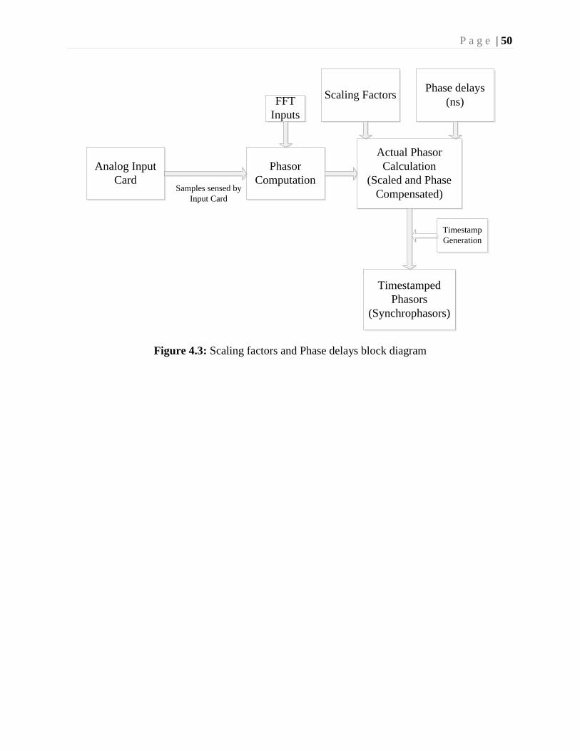
P a g e | 50
Figure 4.3: Scaling factors and Phase delays block diagram
Phasor
Computation
Analog Input
CardSamples sensed by
Input Card
FFT
Inputs
Actual Phasor
Calculation
(Scaled and Phase
Compensated)
Timestamped
Phasors
(Synchrophasors)
Timestamp
Generation
Scaling FactorsPhase delays
(ns)

P a g e | 51
4.4. Phase Delay Calibration
Figure 4.4: Phase delay calculation
The signal generation of the VT Test System (explained in Chapter 3) is capable of
outputting signals with a precise phase angle. The signal generation starts at the 1 PPS and
maintains a constant selected angle. For each of the phases (voltages) a nominal signal with
phase angle of zero degrees is fed (S2 ) to the DUT as shown in Figure 4.4, but the amplifier
causes a considerable phase shift in the output signals. To guarantee that a zero crossing
(negative to positive) occurs at the 1 PPS the phase angle of the original signal (S1) can be
adjusted by an offset angle δ. The value of δ is determined through calibration and used in the
signal generation to obtain a zero crossing on the 1PPS at the output of the VT Test system.
A Tektronix TDS 420 Oscilloscope with a resolution setting of 200 ns was used to
compute the phase delays. The device was equipped with 4 channels and two channels (A and B)
were used for the procedure. Channel A was fed with a 1 PPS (obtained from the port of NI PXI
6682 H Card) signal and channel 2 was fed with the test signal (scaled signal). Both the signals
PPS
Synchronized
Signal
Generation
(Analog
Output Card)
3 Phase
Power
Amplifier
DUT
3 V
3 I
Analog Input
Card
Atte
nu
ato
rs
Sh
un
ts
Phasor Calculation and
Comparison
Ethernet
CommunicationA
B
φ
δ
S1
S3
S2

P a g e | 52
were shown at the same time on the Oscilloscope with a trigger (above 500 mV) on the 1PPS
(had magnitude of 1 volt). The test signal would stay stable with respect to the 1 PPS and the
offset from the zero crossing of the test signal from the 1 PPS was measured. This offset
measured in nanoseconds was used by the phasor computational algorithm to calculate
equivalent phase delay for compensating the error.
The Signal S3 in Figure 4.4 is the signal (phasor calculation) which is rebuilt from the
samples obtained from the Analog Input card of the test system. Once the output signal is
calibrated to obtain a zero crossing at the 1 PPS the phase delays introduced by paths A and B
can be correcting by determining the correcting factors. Any offset (φ) of the phasors (signal S3)
from the 1 PPS accounts for the delays in paths A and B. During calibration these delays are
noted and later used to adjust the calculation of the phasor as shown in Figure 4.2 and 4.3. The
test signals were maintained at a constant magnitude of 70 volts and at a constant frequency of
60 Hz for computing the phase delays. The array (table) labeled as low delay consists of the
computed delay in nanoseconds. The first three values correspond to the delay in voltage
channels of Phase A, B, and Phase C. The next 3 values correspond to the phase delay values of
current channels of Phase A, Phase B and Phase C.
4.5. Calibration Results
The Calibration results obtaining by performing the steps mentioned in sections 4.3 and
4.4 are summarized in the Table 4.1 below. The scaling factors and the phase delays were used
as input parameters in accurate calculation of the actual phasor. The magnitude scaling factors
computed using an Agilent 34401A (Table B.1 of Appendix B) have an uncertainty of .12%
(also .12% TVE). The Phase delays were calculated using a 200 ns resolution on the oscilloscope
with a uncertainty of .007608 % on the Total Vector Error.
Table 4.1: Magnitude Scaling factors and Phase delay values
Phase A
Voltage
Phase B
Voltage
Phase C
Voltage
Phase A
Current
Phase B
Current
Phase C
Current
Magnitude Scaling
Factors
20.9641 20.9642 20.967 19.787 19.815 19.784
Phase Delay
Correction(ns)
22400 23200 21400 -14512 -12303 -14305

P a g e | 53
Chapter 5. Results of PMU Testing
This chapter describes the Steady State Test results and various other DUT issues
reported when four PMUs were tested with the Virginia Tech PMU Test System.
5.1. Steady State Tests
The steady-state performance compliance tests required by IEEE C37.118 include
frequency variation, magnitude variation, phase angle variation, harmonic distortion, out-of-band
signal interference, magnitude unbalanced three-phase signals and phase unbalanced three-phase
signals.
All steady-state tests are performed with a balanced three-phase voltage and current
inputs to the DUT except for the unbalanced tests. The nominal magnitudes for DUT‟s tested
were 70Volts and 5Amperes for 3 PMUs and 110Volts and 5 Amperes for one PMU.
With the applied test conditions the Total Vector Error for the DUT‟s are calculated
from the magnitude and phase difference between the DUT reported phasors and the VT PMU
system computed phasor values. All steady-state performance tests were conducted for two
reporting rates: 30 fps and 60 fps. Tests results are presented in the sections below with graphs of
the maximum, minimum, and mean TVEs during the testing period from the data obtained by the
Virginia Tech Testing System. Compliance limits are given in Table 3 of the IEEE C37.118-
2005 Standard [1] .Table 2.1 illustrates the various conditions and the requirements for the DUT
to pass or fail the tests. The IEEE C37.118-2005 standard defines two compliance levels, Level 0
and Level 1.The range of operation (for obtaining a TVE < %1) are also shown in the Table
2.1(chapter 2). A DUT passes a particular compliance test if the computed TVE is less than 1%
in the defined range. The DUT otherwise fails the compliance test.
The performance of the DUT depends on the quality of the input channels, filter design
and the algorithm used to compute the Fast Fourier Transform for computing the phasor
equivalent of the signal. The device also needs to be calibrated and compensated for accurate
computation of a phasor. The device should be closely locked to the GPS to ensure a good
quality of the timestamps.

P a g e | 54
5.1.1. Steady State Frequency Test
5.1.1.1. Test Description
The frequency of the voltage and current signals is varied from 55 Hz to 65 Hz in steps
of .05 Hz. The magnitude of these signals is maintained at a nominal reference value with the
injected harmonics and the out of band interference within the specified limits of less than 0.2%.
Each step is run for 15 seconds and the TVE% statistics (mean, maximum and median) are
obtained from the number of phasors compared during this period.
Each DUT tested can be analyzed and divided as Level 0 and Level 1 as defined in Table
3 of the IEEE C37.118-2005 standard [1] with TVE<1% within ± 0.5 Hz for Level 0 and ± 5
Hz for Level 1.
5.1.1.2. Test Results
Figures 5.1 to 5.4 show the results obtained for the voltage and current channels at 30
frames/sec and 60 frames/sec respectively. The results obtained can be summarized as shown in
the Table 5.1 below.
Table 5.1: Steady State Frequency variation Test Result
Level 0
Level 1
Frame Rate Voltage Current Voltage Current
30 frames/second Pass Pass Fail Fail
60 frames/second Pass Pass Fail Fail
Table 5.1 shows the final result of the Steady State Frequency Test. The device passes
for Level 0 requirement (± 0.5 Hz) for voltage and current channels at 30 and 60 frames/second
but fails for Level 1 requirement (± 5 Hz) for voltage and current channels at 30 and 60
frames/second.

P a g e | 55
55 56 57 58 59 60 61 62 63 64 65
0.2
0.4
0.6
0.8
1
1.2
1.4
1.6
1.8
2
2.2
TVE (%)
Frequency
Figure 5.2: Results of Steady State Frequency Test for Voltage at 60 f/s
DUT Steady State Voltage Frequency Test 60 frames/sec
V1 MEAN TVE %
V1 MIN TVE %
V1 MAX TVE %
55 56 57 58 59 60 61 62 63 64 65 0
1
2
3
4
5
6
7
8
9
10
11
12
13 13
TVE (%)
DUT Steady State Voltage Frequency Test 30 frames/sec
V1 MEAN TVE %
V1 MIN TVE %
V1 MAX TVE %
Frequency
Figure 5.1: Results of Steady State Frequency Test for Voltage at 30 f/s
f

P a g e | 56
55 56 57 58 59 60 61 62 63 64 65 0.8
1
1.2
1.4
1.6
1.8
2
2.2
2.4
2.6
Frequency
Figure 5.4: Results of Steady State Frequency Test for Current at 60 f/s
DUT Steady State Current Frequency Test 60 frames/sec
I1 MEAN TVE %
I1 MIN TVE %
I1 MAX TVE %
TVE (%)
55 56 57 58 59 60 61 62 63 64 65
1
2
3
4
5
6
7
8
9
10
11
12
Frequency
Figure 5.3: Results of Steady State Frequency Test for Current at 30 f/s
DUT Steady State Current Frequency Test 30 frames/sec
I1 MEAN TVE %
I1 MIN TVE % I1 MAX TVE %
TVE (%)

P a g e | 57
5.1.2. Steady State Magnitude Test
5.1.2.1. Test Description
The magnitude of the voltage and current signals is varied from 10% to 120% of the
nominal voltage in steps of 5% of the nominal. The frequency of these signals is maintained at a
reference value (60 Hz) with the injected harmonics and the out of band interference both within
the specified limits of less than 0.2%.Each step is run for 15 seconds and the TVE% statistics
(mean, maximum and median) are obtained from the number of phasors compared during this
period.
Each DUT tested can be analyzed and classified as Level 0 and Level 1 as defined in
Table 3 of the IEEE C37.118-2005 standard [1] with TVE<1% within 80% to 120% of nominal
magnitude for Level 0 and 10% to 120% of nominal magnitude for Level 1.
5.1.2.2. Test Results
Figures 5.5 to 5.8 show the results obtained for the voltage and current channels at 30
frames/sec and 60 frames/sec respectively. The results obtained can be summarized as shown in
the Table 5.2 below.
Table 5.2: Steady State Magnitude variation Test Result
Level 0
Level 1
Frame Rate Voltage Current Voltage Current
30 frames/second Pass Pass Pass Fail
60 frames/second Pass Pass Pass Pass
Table 5.2 shows the final result of the Steady State Magnitude Test. The device passes
for Level 0 requirement(80% to 120% of nominal magnitude) for voltage and current channels at
30 and 60 frames/second but fails for Level 1 requirement(10% to 120% of nominal magnitude)
for current channels at 30 frames/second.

P a g e | 58
0 20 40 60 80 100 120 0
0.05
0.1
0.15
0.2
0.25
0.3
0.35
0.4
TVE (%)
Magnitude (%)
Figure 5.6: Results of Steady State Magnitude Test for Voltage at 60 f/s
DUT Steady State Voltage Magnitude Test 60 frames/sec
V1 MEAN TVE %
V1 MIN TVE % V1 MAX TVE %
0 20 40 60 80 100 120 0
0.05
0.1
0.15
0.2
0.25
0.3
0.35
0.4
TVE (%)
Magnitude (%)
Figure 5.5: Results of Steady State Magnitude Test for Voltage at 30 f/s
DUT Steady State Voltage Magnitude Test 30 frames/sec
V1 MEAN TVE % V1 MIN TVE % V1 MAX TVE %

P a g e | 59
0 20 40 60 80 100 120
0.4
0.6
0.8
1
1.2
1.4
1.6
1.8
TVE (%)
Magnitude (%)
Figure 5.8: Results of Steady State Magnitude Test for Current at 60 f/s
DUT Steady State Current Magnitude Test 60 frames/sec
I1 MEAN TVE %
I1 MIN TVE %
I1 MAX TVE %
0 20 40 60 80 100 120 0.2
0.3
0.4
0.5
0.6
0.7
0.8
0.9
1
1.1
1.2
TVE (%)
Magnitude (%)
Figure 5.7: Results of Steady State Magnitude Test for Current at 30 f/s
DUT Steady State Current Magnitude Test 30 frames/sec
I1 MEAN TVE %
I1 MIN TVE % I1 MAX TVE %

P a g e | 60
5.1.3. Steady State Phase Angle Test
5.1.3.1. Test Description
For this test the phase angle of the voltage and current signals is varied from -180 to
+180 degrees insteps of 1 degree. The magnitude and frequency of these signals is maintained at
a nominal reference value. Each step is run for 15 seconds and the TVE% statistics (mean,
maximum and median) are obtained from the number of phasors compared during this period.
Each DUT tested can be analyzed and classified as Level 0 and Level 1 as defined in
Table 3 of IEEE C37.118 standard [1] with TVE<1% within ± 180 degrees for Level 0 and ±
180 degrees for Level 1.
5.1.3.2. Test Results
Figures 5.9 to 5.12 are the results obtained for the voltage and current channels at 30
frames/sec and 60 frames/sec respectively. The results obtained can be summarized as shown in
the Table 5.3 below.
Table 5.3: Steady State Phase Angle variation Test Result
Level 0
Level 1
Frame Rate Voltage Current Voltage Current
30 frames/second Pass Pass Pass Pass
60 frames/second Pass Pass Pass Pass
Table 5.3 shows the final result of the Steady State Phase Angle Test. The device
passes for Level 0 and Level 1 requirement (± 180 degrees) for voltage and current channels at
30 and 60 frames/second.

P a g e | 61
-200 -150 -100 -50 0 50 100 150 200
0.29
0.3
0.31
0.32
0.33
0.34
0.35
0.36
0.37
0.38
TVE (%)
Phase
Figure 5.10: Results of Steady State Phase Test for Voltage at 60 f/s
DUT Steady State Voltage Phase Test 60 frames/sec
V1 MEAN TVE %
V1 MIN TVE %
V1 MAX TVE %
-200 -150 -100 -50 0 50 100 150 200
0.32
0.33
0.34
0.35
0.36
0.37
TVE (%)
Phase
Figure 5.9: Results of Steady State Phase Test for Voltage at 30 f/s
DUT Steady State Voltage Phase Test 30 frames/sec
V1 MEAN TVE %
V1 MIN TVE %
V1 MAX TVE %

P a g e | 62
-200 -150 -100 -50 0 50 100 150 200 0.8
0.82
0.84
0.86
0.88
0.9
0.92
0.94
0.96
0.98
1
TVE (%)
Phase
Figure 5.12: Results of Steady State Phase Test for Current at 60 f/s
DUT Steady State Current Phase Test 60 frames/sec
I1 MEAN TVE %
I1 MIN TVE %
I1 MAX TVE %
-200 -150 -100 -50 0 50 100 150 200 0.8
0.82
0.84
0.86
0.88
0.9
0.92
0.94
0.96
0.98
TVE (%)
Phase
Figure 5.11: Results of Steady State Phase Test for Current at 30 f/s
DUT Steady State Current Phase Test 30 frames/sec
I1 MEAN TVE %
I1 MIN TVE %
I1 MAX TVE %

P a g e | 63
5.1.4. Steady State Harmonic Test
5.1.4.1. Test Description
The test follows Table 3 defined in the IEEE C37.118-2005 standard [1]. A 10%
harmonic is added to the Voltage and Current signals .The steps run from 2nd
harmonic to the
50th
harmonic .The base signal (reference signal) is maintained at 100% nominal value for
voltages and currents at a 60 Hz frequency. Each step is run for 15 seconds and the TVE%
statistics (mean, maximum and median) are obtained from the number of phasors compared
during this period. The injected out of band interference is maintained within 0.2% of the
nominal magnitude.
Each DUT tested can be analyzed and classified as Level 0 and Level 1 as defined in
Table 3 of IEEE C37.118 standard [1] with TVE<1% at 1% (of nominal magnitude) harmonic
for Level 0 and 10% (of nominal magnitude) harmonic for Level 1.
5.1.4.2. Test Results
Figures 5.13 to 5.16 show the results obtained for the voltage and current channels at 30
frames/sec and 60 frames/sec respectively. The results obtained can be summarized as shown in
the Table 5.4 below.
Table 5.4: Steady State Harmonic Interference Test Result
Level 0
Level 1
Frame Rate Voltage Current Voltage Current
30 frames/second Pass Pass Pass Pass
60 frames/second Pass Pass Pass Pass
Table 5.4 shows the final result of the Steady State Harmonic Test. The device passes for
Level 0 (1% of 2nd
harmonic to the 50th
harmonic) and Level 1 requirement (10% of 2nd
harmonic to the 50th
harmonic) for voltage and current channels at 30 and 60 frames/second.

P a g e | 64
0 5 10 15 20 25 30 35 40 45 50 0
0.2
0.4
0.6
0.8
1
1.2
TVE (%)
DUT Steady State Voltage Harmonic Test 60 frames/sec
V1 MEAN TVE %
V1 MIN TVE %
V1 MAX TVE %
0 5 10 15 20 25 30 35 40 45 50 0.315
0.515
0.715
0.915
1.115
1.3
TVE (%)
Harmonic Number
Figure 5.13: Results of Steady State Harmonic Test for Voltage at 30 f/s
DUT Steady State Voltage Harmonic Test 30 frames/sec
V1 MEAN TVE % V1 MIN TVE % V1 MAX TVE %
Harmonic Number
Figure 5.14: Results of Steady State Harmonic Test for Voltage at 60 f/s

P a g e | 65
0 5 10 15 20 25 30 35 40 45 50 0.5
0.6
0.7
0.8
0.9
1
1.1
1.2
1.3
TVE (%)
Harmonic Number
Figure 5.16: Results of Steady State Harmonic Test for Current at 60 f/s
DUT Steady State Current Harmonic Test 60 frames/sec
I1 MEAN TVE %
I1 MIN TVE %
I1 MAX TVE %
0 5 10 15 20 25 30 35 40 45 50 0.65
0.7
0.75
0.8
0.85
0.9
0.95
1
1.05
1.1
1.15
TVE (%)
Harmonic Number
Figure 5.15: Results of Steady State Harmonic Test for Current at 30 f/s
DUT Steady State Current Harmonic Test 30 frames/sec
I1 MEAN TVE % I1 MIN TVE % I1 MAX TVE %

P a g e | 66
5.1.5. Steady State Inter-harmonic Test
5.1.5.1. Test Description
The test follows Table 3 defined in the IEEE C37.118-2005 standard [1]. A 10% inter
harmonic is added to the Voltage and Current signals .The steps run from inter-harmonic
frequency band of 0 to 130 Hz .The base signal (reference signal) is maintained at 100%
nominal value for voltages and currents at a 60 Hz frequency. Each step is run for 15 seconds
and the TVE% statistics (mean, maximum and median) are obtained from the number of phasors
compared during this period. The injected harmonics are maintained within 0.2% of the nominal
magnitude. For 30 frames/sec the frequency band requirement is 45 Hz to 75 Hz and for 60
frames/sec the frequency band is 30 Hz to 90 Hz.
Each DUT tested can be analyzed and divided as Level 0 and Level 1 as defined in
Table 3 of IEEE C37.118 standard [1] with TVE<1% at 1% (of nominal magnitude) inter-
harmonic for Level 0 and 10% (of nominal magnitude) inter-harmonic for Level 1.
5.1.5.2. Test Results
Figures 5.17 to 5.20 are the results obtained for the voltage and current channels at 30
frames/sec and 60 frames/sec respectively. The results obtained can be summarized as shown in
the Table 5.5 below.
Table 5.5: Steady State Inter-harmonic Interference Test Result
Level 0
Level 1
Frame Rate Voltage Current Voltage Current
30 frames/second Pass Pass Pass Pass
60 frames/second Pass Pass Pass Pass
Table 5.5 shows the final result of the Steady State Inter-harmonic Test. The device
passes for Level 0 (1% of inter-harmonic signal) and Level 1(10% of inter-harmonic signal)
requirement for voltage and current channels at 30 and 60 frames/second.

P a g e | 67
0 20 40 60 80 100 120 140 0.33
0.34
0.35
0.36
0.37
0.38
0.39
0.4
TVE (%)
Inter-harmonic Frequency
Figure 5.18: Results of Steady State Inter Harmonic Test for Voltage at 60 f/s
DUT Steady State Voltage Inter Harmonic Test 60 frames/sec
V1 MEAN TVE %
V1 MIN TVE %
V1 MAX TVE %
0 20 40 60 80 100 120 140
0.28
0.3
0.32
0.34
0.36
0.38
TVE (%)
Inter-harmonic Frequency
Figure 5.17: Results of Steady State Inter Harmonic Test for Voltage at 30 f/s
DUT Steady State Voltage Inter Harmonic Test 30 frames/sec
V1 MEAN TVE %
V1 MIN TVE %
V1 MAX TVE %

P a g e | 68
0 20 40 60 80 100 120 140 0.76
0.78
0.8
0.82
0.84
0.86
0.88
0.9
0.92
0.94
0.96
TVE (%)
Inter-harmonic Frequency
Figure 5.20: Results of Steady State Inter Harmonic Test for Current at 60 f/s
DUT Steady State Current Inter Harmonic Test 60 frames/sec
I1 MEAN TVE %
I1 MIN TVE %
I1 MAX TVE %
0 20 40 60 80 100 120 140 0.78
0.8
0.82
0.84
0.86
0.88
0.9
0.92
0.94
0.96
TVE (%)
Inter-harmonic Frequency
Figure 5.19: Results of Steady State Inter Harmonic Test for Current at 30 f/s
DUT Steady State Current Inter Harmonic Test 30 frames/sec
I1 MEAN TVE %
I1 MIN TVE %
I1 MAX TVE %

P a g e | 69
5.1.6. Steady State Unbalanced Phase Test
5.1.6.1. Test Description
The phase angle of „Phase B‟ voltage and „Phase B‟ current signals is varied from -60
to +60 degrees in steps of 20 degree. The phase angles of Phase A and Phase C are kept constant
(to the angle of balanced signal) with the frequency of these signals at 60 Hz. Each step is run for
15 seconds and the TVE% statistics (mean, maximum and median) are obtained from the number
of phasors compared during this period. The injected harmonics and the inter harmonics are
within specified limits (0.2% of nominal magnitude).
The DUT should have a TVE% <1 to pass this test.
5.1.6.2. Test Results
Figures 5.21 to 5.24 are the results obtained for the voltage and current channels at 30
frames/sec and 60 frames/sec respectively. The results obtained can be summarized as shown in
the Table 5.6 below.
Table 5.6: Steady State Phase Unbalance Test Result
Frame Rate Voltage Current Voltage Current
30 frames/second Pass Pass Pass Pass
60 frames/second Pass Pass Pass Pass
Table 5.5 shows the final result of the Steady State Unbalanced Phase Test (Phase B
unbalanced). The DUT passes the tests for both 30 frames/second and 60 frames/second.

P a g e | 70
-60 -40 -20 0 20 40 60 0.33
0.35
0.37
0.39
0.41
0.43
0.45
0.47
0.49
0.51
0.53
0.55
0.57
TVE (%)
Phase
Figure 5.22: Results of Steady State Phase Unbalance Test for Voltage at 60 f/s
Figure 5.22.Results of Steady State Phase Unbalance Test for Voltage at 60 f/s
DUT Steady State Voltage Unbalance Phase Test 60 frames/sec
V1 MEAN TVE % V1 MIN TVE % V1 MAX TVE %
-60 -40 -20 0 20 40 60
0.36
0.38
0.4
0.42
0.44
0.46
0.48
0.5
0.52
0.54
0.56
TVE (%)
Phase
Figure 5.21: Results of Steady State Phase Unbalance Test for Voltage at 30 f/s
DUT Steady State Voltage Unbalance Phase Test 30 frames/sec
V1 MEAN TVE %
V1 MIN TVE %
V1 MAX TVE %

P a g e | 71
-60 -40 -20 0 20 40 60 0.8
0.85
0.9
0.95
1
1.05
1.1
1.15
1.2
1.25
TVE (%)
Phase
Figure 5.24: Results of Steady State Phase Unbalance Test for Current at 60 f/s
DUT Steady State Current Unbalance Phase Test 60 frames/sec
I1 MEAN TVE %
I1 MIN TVE %
I1 MAX TVE %
-60 -40 -20 0 20 40 60
0.8
0.85
0.9
0.95
1
1.05
1.1
TVE (%)
Phase
Figure 5.23: Results of Steady State Phase Unbalance Test for Current at 30 f/s
DUT Steady State Current Unbalance Phase Test 30 frames/sec
I1 MEAN TVE %
I1 MIN TVE %
I1 MAX TVE %

P a g e | 72
5.1.7. Steady State Unbalanced Magnitude Test
5.1.7.1. Test Description
The magnitude of „Phase B‟ voltage and „Phase B‟ current signals is varied from 0% to
120% of nominal in steps of 20 %. The magnitudes of Phase A and Phase C is kept at nominal
value with frequency of these signals at 60 Hz. Each step is run for 15 seconds and the TVE%
statistics (mean, maximum and median) are obtained from the number of phasors compared
during this period. The injected harmonics and the inter harmonics are within specified limits
(0.2% of nominal magnitude).
The DUT should have a TVE% <1 to pass this test.
5.1.7.2. Test Results
Figures 5.25 to 5.28 are the results obtained for the voltage and current channels at 30
frames/sec and 60 frames/sec respectively. The results obtained can be summarized as shown in
the Table 5.7 below.
Table 5.7: Steady State Magnitude Unbalance Test Result
Frame Rate Voltage Current Voltage Current
30 frames/second Pass Pass Pass Pass
60 frames/second Pass Pass Pass Pass
Table 5.5 shows the final result of the Steady State Unbalanced Magnitude Test (Phase
B unbalanced). The DUT passes the tests for both 30 frames/second and 60 frames/second.

P a g e | 73
0 20 40 60 80 100 120 140
0.32
0.34
0.36
0.38
0.4
0.42
0.44
0.46
0.48
0.5
TVE (%)
Magnitude(%)
Figure 5.26: Results of Steady State Magnitude Unbalance Test for Voltage at 60 f/s
DUT Steady State Voltage Unbalance Magnitude Test 60 frames/sec
V1 MEAN TVE %
V1 MIN TVE %
V1 MAX TVE %
0 20 40 60 80 100 120 140
0.34
0.36
0.38
0.4
0.42
0.44
0.46
0.48
0.5
TVE (%)
Magnitude (%)
Figure 5.25: Results of Steady State Magnitude Unbalance Test for Voltage at 30 f/s
DUT Steady State Voltage Unbalance Magnitude Test 30 frames/sec
V1 MEAN TVE %
V1 MIN TVE %
V1 MAX TVE %

P a g e | 74
0 20 40 60 80 100 120 140 0.78
0.8
0.82
0.84
0.86
0.88
0.9
0.92
0.94
0.96
TVE (%)
DUT Steady State Current Unbalance Magnitude Test 60 frames/sec
I1 MEAN TVE % I1 MIN TVE % I1 MAX TVE
%
0 20 40 60 80 100 120 140 0.8
0.82
0.84
0.86
0.88
0.9
0.92
0.94
0.96
0.98
1
TVE (%)
Magnitude (%)
Figure 5.27: Results of Steady State Magnitude Unbalance Test for Current at 30f/s
DUT Steady State Current Unbalance Magnitude Test 30 frames/sec
I1 MEAN TVE %
I1 MIN TVE %
I1 MAX TVE %
Magnitude (%)
Figure 5.28: Results of Steady State Magnitude Unbalance Test for Current at 60f/s
Figure 7.l.Results of Steady State Magnitude Unbalance Test for Current at 60f/s

P a g e | 75
5.2. DUT Latency and other Issues
5.2.1. DUT Latency
The DUT PMU should stream out a data frame immediately as soon as it is generated
and time stamped. The data frame should reach the destination (PDC PMU connection tester etc)
with minimal delay. There could be delays due to various reasons like network congestion, type
of communication protocol etc. This chapter discusses the delays that were noticed while
transmitting the data frames by the DUTs.
Figure 5.29: Front panel of latencytry_vijay.vi
Figure 5.29 shows the front panel of the vi that was developed to compute the latency of
the DUT PMU. The functional block diagram description is explained in Figure 3.11 of section
3.4.2. .Figure 5.29 shows a snapshot of the time differences for a period of 1011 data frames.
Three DUT‟s are tested for the data frame differences and the results are discussed below.

P a g e | 76
5.2.1.1. DUT A Latency
Figures 5.30 and 5.31 show a snapshot of the differences obtained between timestamps
of two successive data frames from DUT A. The timestamps which were used to compute these
differences are generated by the time stamping card whenever a data frame arrives at the TCP
port. From Figure 5.30 it can be seen that the difference between the data frames varies from 8
ms to 50 ms, and that the DUT is trying to maintain a difference close to 33.333 ms (1000/30
ms) on an average for a stream rate of 30 frames/sec. Figure 5.31 shows fewer data frames
(zoomed) confirming the delays between the data frames.
Figure 5.30: Time difference between data frames for DUT A
Figure 5.31: Time difference between data frames (zoomed) for DUT A

P a g e | 77
5.2.1.2. DUT B Latency
Figures 5.32 and 5.33 show a snapshot of the differences obtained between timestamps
of two successive data frames for DUT B. From Figure 5.32 it can be seen that the difference
between the data frames varies from 4 ms to 170 ms, and that the DUT is trying to maintain a
difference close to 33.333 ms (1000/30 ms) on an average for a stream rate of 30 frames/sec.
Figure 5.33 shows fewer data frames (zoomed) confirming the delays between the data frames.
This device showed a peculiar behavior of trying to send few sets of data frames very fast (much
smaller than 33.3 ms) and then sending a data frame after a large delay (much greater than 33.3
ms).Though the time differences fluctuate over a large range the average time difference is tried
to maintain at 33.333 ms.
Figure 5.32: Time difference between data frames for DUT B
Figure 5.33: Time difference between data frames (zoomed) for DUT B

P a g e | 78
5.2.1.3. DUT C Latency
Figures 5.34 and 5.35 show a snapshot of the differences obtained between
timestamps of two successive data frames for DUT B. From Figure 5.34 it can be seen that the
difference between the data frames varies from 2 ms to 170 ms, and that the DUT is trying to
maintain a difference close to 33.333 ms (1000/30 ms) on an average for a stream rate of 30
frames/sec. Figure 5.35 shows fewer data frames confirming the delays between the data frames.
This device also showed a peculiar behavior of trying to send few set of data frames very fast
(much smaller than 33.3 ms) and then sending a data frame after a large delay(much greater than
33.3 ms).Though the time differences fluctuate over a large range the average time difference is
maintained at 33.333 ms.
The IEEE C37.118-2005 standard defines the stream rate of the PMUs in the range of
10-60 frames/sec .The DUT‟s try to maintain this promised frame rate but not necessarily a
difference of 1/frame rate between the data frames. A similar behavior has been seen with both
the TCP and UDP connections with minimal network latencies. Thanks to these results the
frames delay is a new test performed by the system. After evaluating the test results on the first 4
PMUs PJM does not accept and average rate over a second acceptable unless the delay between
frames is uniformly distributed.
Figure 5.34: Time difference between data frames for DUT C
Figure 5.35: Time difference between data frames (zoomed) for DUT C
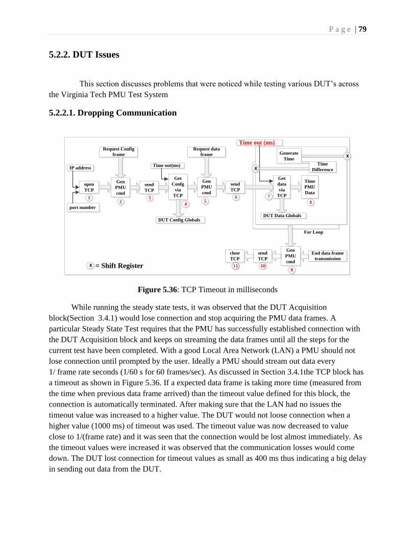
P a g e | 79
5.2.2. DUT Issues
This section discusses problems that were noticed while testing various DUT‟s across
the Virginia Tech PMU Test System
5.2.2.1. Dropping Communication
Figure 5.36: TCP Timeout in milliseconds
While running the steady state tests, it was observed that the DUT Acquisition
block(Section 3.4.1) would lose connection and stop acquiring the PMU data frames. A
particular Steady State Test requires that the PMU has successfully established connection with
the DUT Acquisition block and keeps on streaming the data frames until all the steps for the
current test have been completed. With a good Local Area Network (LAN) a PMU should not
lose connection until prompted by the user. Ideally a PMU should stream out data every
1/ frame rate seconds (1/60 s for 60 frames/sec). As discussed in Section 3.4.1the TCP block has
a timeout as shown in Figure 5.36. If a expected data frame is taking more time (measured from
the time when previous data frame arrived) than the timeout value defined for this block, the
connection is automatically terminated. After making sure that the LAN had no issues the
timeout value was increased to a higher value. The DUT would not loose connection when a
higher value (1000 ms) of timeout was used. The timeout value was now decreased to value
close to 1/(frame rate) and it was seen that the connection would be lost almost immediately. As
the timeout values were increased it was observed that the communication losses would come
down. The DUT lost connection for timeout values as small as 400 ms thus indicating a big delay
in sending out data from the DUT.
Gen
PMU
cmd
Request data
frame
send
TCP
open
TCP
IP address
port number
Gen
PMU
cmd
send
TCP
Get
Confg
via
TCP
Request Config
frame
DUT Config Globals
Get
data
via
TCP
Time
PMU
Data
DUT Data Globals
For Loop
Gen
PMU
cmd
End data frame
transmission
send
TCP
close
TCP
12
3
45
6 7
8
91011
Time out(ms)
Time out (ms)
Generate
TimeTime
Difference
X
X
X = Shift Register

P a g e | 80
5.2.2.2. Incorrect Phasor Calculation
Figure 5.37: Steady State Voltage Frequency Test 1
Figure 5.37 shows the TVE % error that was obtained when a DUT C was tested for a
Voltage Steady State Frequency test (30 frames) with frequency varied from 55 Hz to 65 Hz in
steps of .05 Hz. Each step ran for 15 seconds and the TVE% mean, maximum and minimum
were calculated for each step for a period of 15 seconds (450 frames).It was observed using a
PMU Connection Tester (obtained as a part of openPDC freeware) that the DUT was sending
useful information only after a delay of few seconds, i.e. the DUT would not send actual signal
information (in phasors) until a few seconds have elapsed and delay would depend on the signal
frequency . The Figure 5.38 shows the same test repeated but with each step run for 60 seconds.
The TVE % mean, maximum and minimum statistics were calculated only by considering the
last 20 seconds of each step. The results were improved when the data for first few seconds (40
seconds) was neglected for TVE comparison. The device responded quite well for frequencies of
XX.Y(Y=0,1,2….9) but had higher TVE error for XX.05. This DUT C manufacturers were
notified of the problem and it was mentioned that they designed their DUT to accurately
compute phasors for frequencies with steps of .1Hz (XX.1, XX.2…) in their algorithm. The
device was also designed to take some time to estimate the correct frequency. The VT test
system runs 15 seconds for each step for computing the necessary statistics. The device was
55 56 57 58 59 60 61 62 63 64 65 0
50
100
150
200
250
300
TVE (%)
Frequency
DUT C Steady State Voltage Frequency Test 30 frames/sec
V1 MEAN TVE %
V1 MIN TVE % V1 MAX TVE %
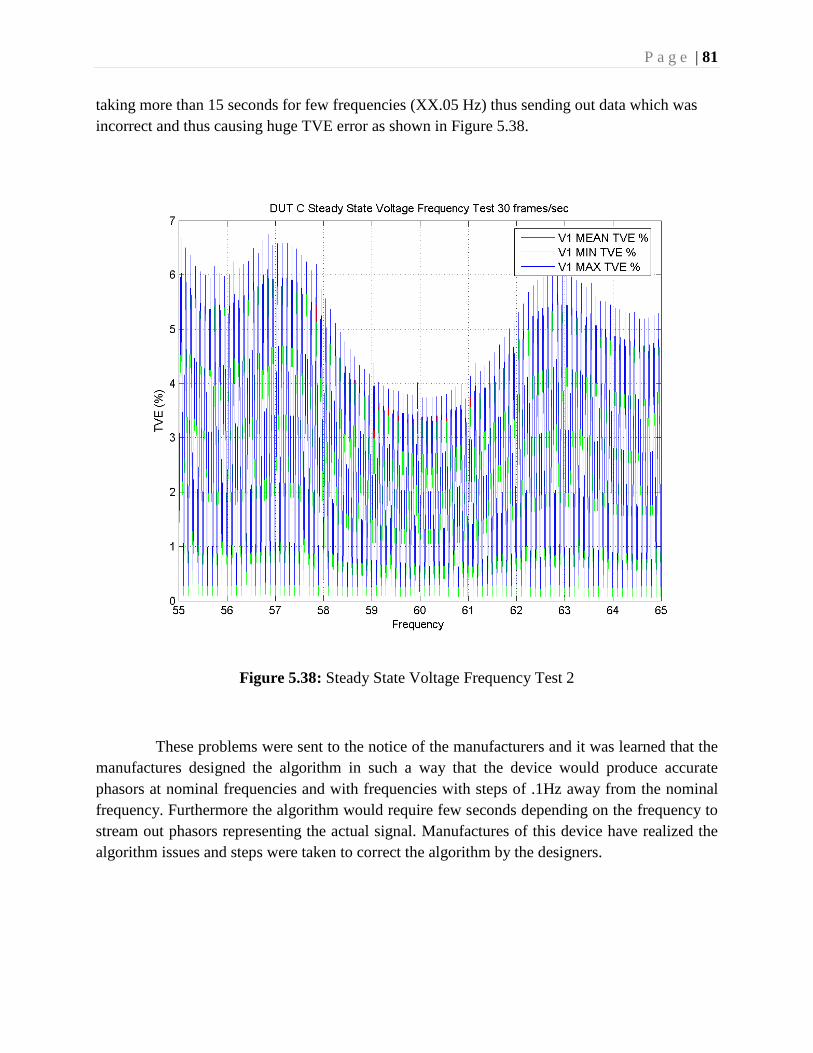
P a g e | 81
taking more than 15 seconds for few frequencies (XX.05 Hz) thus sending out data which was
incorrect and thus causing huge TVE error as shown in Figure 5.38.
Figure 5.38: Steady State Voltage Frequency Test 2
These problems were sent to the notice of the manufacturers and it was learned that the
manufactures designed the algorithm in such a way that the device would produce accurate
phasors at nominal frequencies and with frequencies with steps of .1Hz away from the nominal
frequency. Furthermore the algorithm would require few seconds depending on the frequency to
stream out phasors representing the actual signal. Manufactures of this device have realized the
algorithm issues and steps were taken to correct the algorithm by the designers.
P a g e | 82
Chapter 6. Conclusions and Future Work
This chapter provides a summary of the work presented in the thesis. A brief discussion
of the future work is also included.
6.1. Summary and Conclusion
Phasor Measurement Units are beginning to play a key role in providing valuable
information in building a reliable and robust power system. With a diverse and new number of
manufacturers providing PMU functionality in different IEDs the adherence to the existing
standards has become a key issue in the value of the information provided by these devices. This
thesis present the work performed to develop a PMU testing system at Virginia Tech in
accordance with the existing standards and previous developments at the National Institute of
Standards and Technology. The various issues that were encountered while successfully
building the test system have been discussed and the solution implemented for solving these
issues have been described.
My main contributions and achievements for building a Steady State PMU Test System
at Virginia Tech are summarized as follows.
A Synchronized Signal Generation block capable of generating all the necessary test
signals required to perform the various steady state compliance tests required by the
IEEE C37.118 - 2005 and future standard was built.
The compatibility issues in the NIST based code caused by the differences in the
hardware set-up in the VT Test System were successfully solved and all Analog Input
and Output cards were synchronized to an external GPS clock.
A fully functional VT PMU Steady State Test System coherent with the existing NIST
PMU Steady State System has been developed and tested.
The VT PMU Steady State System was calibrated to obtain accurate scaling factors for
the shunts and attenuators used in the system. Phase delays were also calculated and
compensated for accurate phasor computation.
Four PMUs from different manufacturers have been tested as per the IEEE C37.118-
2005 standard steady state performance requirements and the results have been
discussed with the manufacturers and PJM.
Specific problem of PMUs discovered through their evaluation have been analyzed,
documented and acknowledged by the PMU manufacturers. Possible causes have been
presented to the individual companies.

P a g e | 83
6.2. Future Work
The following are key problems that need to be solved to enhance the accuracy and
capability of the VT PMU Testing system:
The shunts used in the existing Virginia Tech PMU Test System can be upgraded and
calibrated to match the accuracy range of the Analog Input Card.
The Analog Input Card has the promised accuracy only if the value of the input signal is
above 26mv.The steady state magnitude test requires the test signals magnitude to vary
from 10% to 120% of the nominal magnitude. The 10% of the nominal 5 amp currents is
sensed through the shunts as a 25mV input to the Analog Input Card. New shunts with a
higher resistance can provide voltages well within the accuracy range of the input card
thus improving the system performance for sensing currents of lesser magnitudes.
The existing standard IEEE C37.118-2005 primarily focuses on the steady state
requirements of a Phasor Measurement Unit. A Phasor Measurement Unit is capable of
performing well even under transient conditions [1]. Steps are being taken to revise and
include dynamic requirements to the existing standard.
The Steady State Test System can be modified and extended to build a Dynamic Steady
State System to test PMUs as required by the future IEEE C37.118.1 standard. The new
standard is also expected to include some changes to the existing steady state
requirements. The previously defined Level 0 and Level 1 compliance requirements [1]
will be revised and replaced with P and M class requirements. The range of operation
over which the TVE < 1% is defined for P and M class would be different for some tests
to those used for Level 0 and Level 1 class in the existing standard.
A certification from the National Institute of Standards and Technology would ensure
accuracy and reliability of the Virginia Tech PMU Steady State Test System. The VT
Test System and the test results obtained while testing various PMUs can be traceable to
NIST and thus could be compared to test results from other institutions and from the
equipment manufacturers.
The existing Steady State Test System can be modified to accommodate for the
anticipated changes in IEEE C37.118.1 standard to be released in near future. An
additional feature of automatically sensing the ambient temperature while performing a
test could be included. A new function can be integrated into the existing system to
include ambient temperature information in the test reports.

P a g e | 84
References
[1]. IEEE Standard for Synchrophasors for Power Systems, IEEE Standard C37.118-2005,
March, 2006.
[2]. Ken Martin & Tony Faris, Bonneville Power Administration (BPA) John Hauer ,
Pacific Northwest National Laboratories (PNNL) ,Standardized Testing of Phasor
Measurement Units, Fault and Disturbance Analysis Conference 2006, Georgia Tech,
Atlanta, GA.
[3]. Kyriakides, E.; Heydt, G.T. , Synchronized measurements in power system operation:
International trends and research , Power and Energy Society General Meeting, 2010
IEEE , vol., no., pp.1-3, 25-29 July 2010.
[4]. Stenbakken, G.; Nelson, T., Static Calibration and Dynamic Characterization of PMUs
at NIST, Power Engineering Society General Meeting, 2007. IEEE , vol., no., pp.1-4,
24-28 June 2007.
[5]. National Instruments, NI PXIe-1062Q User Manual, Feb 2010.
[6]. The Virginia Tech Calibration System, Javier O. Fernandez, May 3, 2011.
[7]. IEEE Standard for Synchrophasers for Power Systems, IEEE Std 1344-1995(R2001) ,
vol., no., pp.i, 1995.
[8]. National Instruments, NI 6356/6358 Specifications. NI PXIe-6356/6358 technical
data, Aug 2010.
[9]. National Instruments, NI 6731/6733 Specifications. NI PXI-6731/6733 technical
data, June 2007.
[10]. National Instruments, NI PXI-6682 and PXI-6682H Timing and Synchronization
Modules for PXI. NI PXI-6682 Series User Manual, March 2009.
[11]. Arbiter Systems, Model 1084A/B/C GPS Satellite Clock, Arbiter 1084B datasheet,
Dec.2010.
[12]. Depablos,J.;Centeno,V.;Phadke,A.G.;Ingram,M.,Comparative testing of synchronized
phasor measurement units, Power Engineering Society General Meeting, 2004. IEEE ,
vol., no., pp. 948- 954 Vol.1, 6-10 June 2004.
[13]. ONS PMU Certification Test Report, Certification Test Report for SEL 451,August
17, 2009.

P a g e | 85
[14]. Burnett, R.O., Jr.; Butts, M.M.; Cease, T.W.; Centeno, V.; Michel, G.; Murphy, R.J.;
Phadke, A.G.; , Synchronized phasor measurements of a power system event,Power
Systems, IEEE Transactions on , vol.9, no.3, pp.1643-1650, Aug 1994.
[15]. Final Report on the August 14, 2003 Blackout in the United States and Canada:
Causes and Recommendations, April 2004.
[16]. Stenbakken, G.; Nelson, T.; , Static Calibration and Dynamic Characterization of
PMUs at NIST, Power Engineering Society General Meeting, 2007. IEEE , vol., no.,
pp.1-4, 24-28 June 2007.
[17] . Phadke, A.G.; , Synchronized phasor measurements-a historical overview,
Transmission and Distribution Conference and Exhibition 2002: Asia Pacific.
IEEE/PES , vol.1, no., pp. 476- 479 vol.1, 6-10 Oct. 2002.
[18]. Agilent Technologies, Agilent 34401A Multimeter Data sheet , Accuracy
Specifications, USA, October 11, 2011.

P a g e | 86
Appendix A. Lab View Block Diagrams
Figure A.1: Lab View Block Diagram Implementation of 1 Phase FM, AM Signal Generation

P a g e | 87
Figure A.2: Lab View Block Diagram Implementation of 1 Phase FM, AM and HM Signal
Generation

P a g e | 88
Figure A.3: Lab View Block Diagram Implementation of 3 Phase FM, AM and HM Signal
Generation
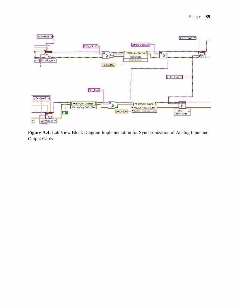
P a g e | 89
Figure A.4: Lab View Block Diagram Implementation for Synchronization of Analog Input and
Output Cards

P a g e | 90
Figure A.5: Lab View Block Diagram Implementation of Latency Calculation

P a g e | 91
Figure A.6: Lab View Block Diagram Computing VT Test System Phasors

P a g e | 92
Appendix B. AGILENT 34401A Technical Specifications
Table B.1: Accuracy Specifications of Agilent 34401 A [18]


![NASPI for NERC OC 121212.pptx [Read-Only] · 2019. 2. 22. · Title: Microsoft PowerPoint - NASPI for NERC OC 121212.pptx [Read-Only] Author: D3P345 Created Date: 12/16/2011 1:36:49](https://img.pdfslide.net/doc/110x75/60cfcc177baddb0e533a9551/naspi-for-nerc-oc-read-only-2019-2-22-title-microsoft-powerpoint-naspi.jpg)