Embed Size (px)
Citation preview

STM32 F-4 Series 2MB
High performance Cortex M4 DSC
MCD Marketing team

STM32 F4 1MB
2
• Cortex M4 w/FPU 168 MHz
• pin-to-pin compatible with STM32F2
• More SRAM (192KB)
• Same IPS as STM32F2
• I2S: now full duplex
• New RTC sub second precision
• Faster serial I/F
• Faster ADC
• 64 pins to 176 pins
• 1.7V-3.6V Supply
CORTEX M4 CPU+ MPU
+ FPU 168 MHz 192KB SRAM
AP
B2
(max 1
68M
hz)
3x 12-bit ADC 24 channels / 2.4Msps
3x I2C
80/112/140 I/Os
Up to 16 Ext. ITs
2x6x 16-bit PWM Synchronized AC Timer
2x Watchdog (independent & window)
5x 16-bit Timer
JTAG/SW Debug
XTAL oscillators 32KHz + 8~25MHz
Power Supply Reg 1.2V
POR/PDR/PVD
DMA
16 Channels
Nested vect IT Ctrl
2x DAC + 2 Timers
2 x USART/LIN
1 x SPI
Bridge
Bridge
1 x Systic Timer
PLL Clock Control
RTC / AWU
APB1
(max 84MHz)
4KB backup RAM
ETM
USB 2.0 OTG HS
Ethernet MAC
10/100, IEEE1588
Fla
sh
I/F
1MB Flash Memory
External Memory Interface
Encryption
Camera Interface
USB 2.0 OTG FS
4x USART/LIN
1x SDIO
Int. RC oscillators 32KHz + 16MHz
AHB1
(max 168Mhz)
AHB2
(max 168Mhz)
3 x 16bit Timer
AR
M ®
32-b
it m
ult
i-A
HB
bu
s m
atr
ix
Arb
iter
(max 1
20M
Hz)
2x 32-bit Timer
2x CAN 2.0B
2 x SPI/I2S
Temp Sensor
USB 2.0 OTG HS

STM32 F4 2MB
3
• Cortex M4 w/FPU, 168 MHz
• full compatible F2/F4
• Dual Bank 2 x 1MB Flash
• 256KB SRAM
• FMC with SDRAM Support, 32-bit data on 208-pin and 176 packages, 16-bit else
• Serial Audio I/F with PCM/TDM support
• TFT LCD Controller with DMA-2D
• Hash: supporting SHA-2 and GCM
• More serial com and more fast timers running at Fcpu
• 100-pins to 208-pins
CORTEX M4 CPU+ MPU
+ FPU 168 MHz 256KB SRAM
AP
B2
(max 1
68 M
Hz)
3x 12-bit ADC 24 channels / 2.4Msps
3x I2C
82/114/140/ I/Os
Up to 16 vectors
Ext. ITs
2x6x 16-bit PWM Synchronized AC Timer
2x Watchdog (independent & window)
5x 16-bit Timer
JTAG/SW Debug
XTAL oscillators 32KHz + 4~26MHz
Power Supply Reg 1.2V
POR/PDR/PVD
DMA
16 Channels
Nested vect IT Ctrl
2x DAC + 2 Timers
4 x USART/LIN
4 x SPI
Bridge
Bridge
1 x Systic Timer
PLLs Clock Control
RTC / AWU
APB1
(max 84MHz)
4KB backup RAM
ETM
Ethernet MAC 10/100,
IEEE1588
Fla
sh
I/F
2MB Flash Memory Dual
Bank
External Memory Interface with SDRAM
Encryption
Camera Interface
USB 2.0 OTG FS
4x USART/LIN
1x SDIO
Int. RC oscillators 32KHz + 16MHz
AHB1
(max 168MHz)
AHB2
(max 168 MHz)
3 x 16bit Timer
AR
M ®
32-b
it m
ult
i-A
HB
bu
s m
atr
ix
Arb
iter
(max 1
68M
Hz)
2x 32-bit Timer
2x CAN 2.0B
2 x SPI/I2S
Temp Sensor
USB 2.0 OTG HS
LCD Controller
SAI
DMA-2D
New feature
STM32 F4 2MB in a few words

STM32 F4 2MB Application targets
Consumer
• HMI in for appliances
• DAB, Car Radio and
infotainment (China)
• Home audio, Switch box,
Headset
Industrial and Medical
• Control panels with LCD screens for alarm systems, High-end meters, Factory automation
• Medical : Respiratory equipment, Patient monitor
• EPOS : scanners,cash registers, tax machines, Vending machine, Printers
• Industrial AC servos, General-purpose inverters, solar inverters and robots
• Surveillance camera
5

STM32 F4 portfolio

STM32 F40x/41x
1MB Flash Die
In production now
STM32 F42x/43x
2MB Flash Die
Samples (Steps 1 and 2) December 2012 Step 1: Production Jan 2013
Step 2: Production May/June 2013 (depending on package)
7
Flash Size
(bytes)
512 K
100 pins
LQFP
64 pins
LFQFP
144 pins
LQFP
1 MB
176 pins
LQFP/UFBGA
STM32 F4 Roadmap
Pin count
2 MB
208/216 pins
LQFP/TFBGA
90 pins
WLCSP

8
Flash Size
(bytes)
512 K
1MB
STM32 F4 complete portfolio
Pin count
STM32F405OG
192KB SRAM E
STM32F405VG
192KB SRAM E
STM32F405ZG
192KB SRAM E
STM32F407VG
192KB SRAM E
STM32F407ZG
192KB SRAM E
STM32F407IG
192KB SRAM E
Ethernet,,camera IF
STM32F407VE
192KB SRAM E
STM32F407ZE
192KB SRAM E
STM32F407IE
192KB SRAM E
2MB
STM32F405RG
192KB SRAM E
STM32F405OE
192KB SRAM
C
S
P
C
S
P
100 pins
LQFP
144 pins
LQFP/WLCSP*
176 pins
LQFP/UFBGA
208/216 pins
LQFP/TFBGA
64 pins
LFQFP
90 pins
WLCSP
STM32F427VI
256KB SRAM E
STM32F427ZI
256KB SRAM E
STM32F427II
256KB SRAM E
STM32F429II
256KB SRAM E
STM32F429BI
256KB SRAM E
STM32F427VG
256KB SRAM E
STM32F427ZG
256KB SRAM E
STM32F427IG
256KB SRAM E
STM32F429IG
256KB SRAM E
STM32F429BG
256KB SRAM E
L
C
D
L
C
D
L
C
D
L
C
D
STM32F429VI
256KB SRAM E
STM32F429ZI
256KB SRAM E
L
C
D
L
C
D
STM32F429VG
256KB SRAM E
STM32F429ZG
256KB SRAM E
L
C
D
L
C
D
*WLCSP on F4x9 part#s only
Ethernet, 2xUSB
OTG, camera IF, all
new features)
Ethernet, 2xUSB
OTG, camera IF, all
new features +LCD

STM32 F4 2MB
First Technical slides
Applications Support Solution Team

10
STM32F4x 1MB STM32F4x 2MB
More
Peripheral
instantiation
3xSPI ( 2xI2S) 6xSPI ( 2xI2S)
4xUSART + 2xUART 4xUSART + 4xUART
New
Peripherals
- 1xSAI (Serial Auto Interface)
1xLCD-TFT controller
- DMA2D (improves graphic performance)
STM32 F4 2MB versus STM32 F4 1MB

11
STM32F4x 1MB STM32F4x 2MB
Pinout
Up to 140 I/Os
LQFP64, WLCSP90, LQFP100, LQFP144,
LQFP176, UFBGA176 packages
Up to 168 I/Os
LQFP100, LQFP144, WLCSP144,
LQFP176, UFBGA176, LQFP208, UFBGA208
packages
- New remap of I2S3_SD and on PD3 and PD6
- New remap of DCIM_D2, DCMI_D3, DCMI_D8 to
DCMI_D13
Peripheral
same as
STM32 F4
1x RTC/AWU w cal.
IWDG and WWDG
1xDCMI(14-Bit)
16 -Stream DMA
1xCRC
1xSDIO
1x USB 2.0 FS Device/host/OTG
1x USB 2.0 HS Device/device/host/OTG
2x CAN 2.0B
1xEthernet
3x ADC12bit/ 0.41µs/24ch
2x DAC 12bit
STM32 F4 2MB versus STM32 F4 1MB

STM32 F4 2MB: Facts sheet
Key features Benefits
Display: LCD-TFT controller and DMA2D HMI design, cost reduction vs chip on glass
for mid size LCDs (5.5” sweet spot)
Audio: SAI with dedicated PLL
The SAI and the 2xI2S peripherlas can
achieve two different sampling rates with
best accuracy.
External Memory Interface with SDRAM
and external bus up to 32-Bit
Twice more performance vs 16-bit (on 176
and 208 packages) ,
SDRAM available on 144-pin package (16-
bit only)
Crypto and Hash More capabilities, extended addressable
market
More IPs instantiation: UARTs, SPIs
More capabilities, extended addressable
market (IO link master, audio applications
using multi MEMS microphones)
STOP Mode current consumption Improved stop mode consumption versus
STM32 F4 1MB
I2C with digital Filter
More robust designs. Filter spikes with a
length up to 15 APB clock periods. Digital
filter can be enabled/Disabled

LCD-TFT Display Controller
First Technical Slides
NEW

Graphics on STM32
MMS/MCD Applications

Overview
10/25/2013 STM32 Graphic
15

STM32 Solution for Graphics
• STM32 offers a unique graphical capability in the Cortex-M based
MCU perimeter
• Real TFT Controller for optimum display control
• External memory interface to connect both Flash for static content and SRAM or
SDRAM for dynamic content and frame buffer
• On-chip hardware acceleration deeply coupled with graphical library
• Standard graphical library taking advantage of on-chip graphical acceleration
16
10/25/2013 Presentation Title

Graphical Flow 17
10/25/2013 STM32 Graphic
Font 1
Text 1
Next Prev
• The frame buffer is transferred to the display through a
dedicated hardware interface
• Graphical oriented microcontroller are offering a TFT
controller to drive directly the display
• The frame buffer must be sent at 60fps to have a perfect
image color and stability (independently from the
animation fps)
Step 2 : Displaying the frame buffer
• The frame buffer is build by composing graphical primitive
• This operation is done by the CPU running a graphical
library software
• It can be accelerated by a dedicated hardware used with
the CPU through the graphical library
• More often the frame buffer can be updated, more fluent
will be the animations (animation fps)
Step 1 : Creating the content in a frame buffer

Architecture with TFT Controller 18
10/25/2013 STM32 Graphic
Bus Matrix
TFT
Controller Cortex-M4
Internal
Flash
Internal
SRAM
External
Memory
Controller
• Microcontroller are tagged “graphical” as soon as they offer a TFT controller
• But none of them are focusing on acceleration solutions for frame buffer
generation whereas it’s the most CPU consuming task
• All the graphical library is running on the CPU

Architecture without TFT Controller 19
10/25/2013 STM32 Graphic
Bus Matrix
External
DMA Cortex-M4
Internal
Flash
Internal
SRAM Timer
• One alternative is to use an external DMA/memory controller with a timer
• This is not a reliable solution
• Bandwidth of external memory is too limited
• TFT is used out of its specification to get this solution working
• No acceleration feature is available

STM32F42x/F43x Architecture 20
10/25/2013 STM32 Graphic
Bus Matrix
TFT
Controller Cortex-M4
Internal
Flash
Internal
SRAM
External
Memory
Controller
DMA2D
• TFT controller allows the interfacing
• DMA2D provides a true graphical acceleration
• DMA2D offloads the CPU for operations like rectangle filling, rectangle
copy (with or without pixel format conversion), and image blending
• DMA2D goes faster than the CPU for the equivalent operation

TFT Controller
10/25/2013 STM32 Graphic
21
Purpose of a TFT Controller
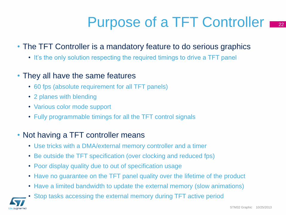
• The TFT Controller is a mandatory feature to do serious graphics
• It’s the only solution respecting the required timings to drive a TFT panel
• They all have the same features
• 60 fps (absolute requirement for all TFT panels)
• 2 planes with blending
• Various color mode support
• Fully programmable timings for all the TFT control signals
• Not having a TFT controller means
• Use tricks with a DMA/external memory controller and a timer
• Be outside the TFT specification (over clocking and reduced fps)
• Poor display quality due to out of specification usage
• Have no guarantee on the TFT panel quality over the lifetime of the product
• Have a limited bandwidth to update the external memory (slow animations)
• Stop tasks accessing the external memory during TFT active period
10/25/2013 STM32 Graphic
22

Benefit of a TFT Controller 23
10/25/2013 STM32 Graphic
Bus Matrix
TFT
Controller Cortex-M4
Internal
Flash
Internal
SRAM
External
Memory
Controller
DMA2D
Dedicated interface : In spec with the TFT panel timings & 60fps
Dedicated interface : Maximum speed & bandwidth
Mix of several memories (Flash, SRAM & SDRAM)

LCD-TFT controller implementation details
• New AHB bus Master on the bus matrix
• Flexible programming display parameters
• Display control signals
• Flexible color format
• Multi-Layer Support
• Windowing
• Blending
• Flexible programmable parameters for each layer (2 layers max)
• Onchip memory or External memory can be used as Frame buffer
24

LCD-TFT architecture 25
AH
B M
as
ter
Inte
rfac
e
Layer1
LCD_G[7:0]
LCD_B[7:0]
FIFO
16x32b
Layer2
FIFO
16x32b
AH
B B
us M
atr
ix
AP
B I
nte
rfac
e
Configuration
registers
Synchoronous
Timings
Generation,
Blending
Dithering
LCD_CLK
LCD_HSYNC
LCD_VSYNC
LCD_DE
LCD_R[7:0]
LC
D P
an
el

LCD-TFT Signals
26
LCD-TFT Signals Description
LCD_CLK Clock output
LCD_HSYNC Horizontal Synchronization
LCD_VSYNC Vertical Synchronization
LCD_DE Data Enable
LCD_R[7:0] 8-Bits Red data
LCD_G[7:0] 8-Bits Green data
LCD_B[7:0] 8-Bits Blue data

Main Features - (1/2)
• 24-bit RGB Parallel Pixel Output; 8 bits-per-pixel ( RGB888)
• AHB 32-Bit master with burst access up to 16 words to any system
memory
• Dedicated FIFO per Layer (depth of 16 word)
• Programmable timings to adapt to targeted display panel.
• HSYNC pulse , VSYNC pulse , VBP, HBP, VFP, HFP
• Programmable Polarity for
• HSYNC, VSYNC, Data Enable
• Pixel clock
• Up to 8 programmable color format per layer
• Supports only TFT ( no STN)
27

Main Features - (2/2)
• Programmable display Size
• Supports QVGA, QWVGA and VGA
• Programmable Background color
• 24-bit RGB, applied when a layer is disabled.
• Multi-Layer Support with blending ( Supports up to 2 layers)
• Dithering* (2-bits per color channel (2,2,2 for RGB))
• *Combination of adjacent pixels to simulate the desired shade
• New programmed values can be loaded immediately at run time or
during Vertical blanking
• 2 Interrupts generated on 4 event Flags
28

Layer Programmable Parameters (1/2)
• Window position
• Window Size
• Pixel Format
• Up to 8 programmable pixel format : ARGB8888 , RGB888, RGB565, ARGB1555,
ARGB4444, L8, A88, A44)
29
POS_X
PO
S_Y
WIDTH
HE
IGH
T
LAYER
Active Display AREA
Layer Programmable Parameters (2/2)
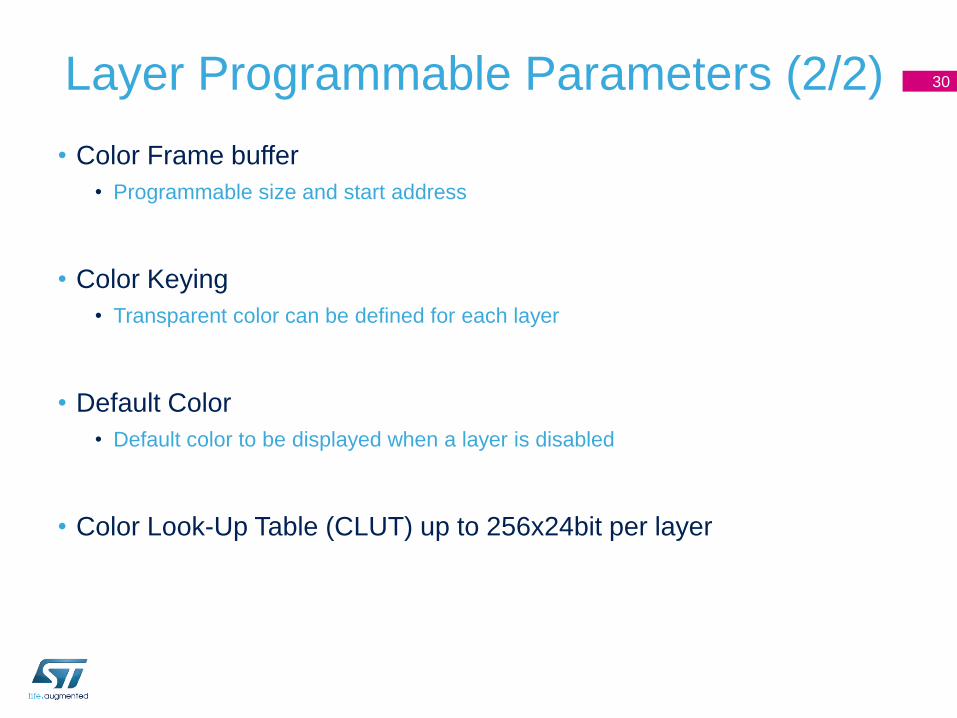
• Color Frame buffer
• Programmable size and start address
• Color Keying
• Transparent color can be defined for each layer
• Default Color
• Default color to be displayed when a layer is disabled
• Color Look-Up Table (CLUT) up to 256x24bit per layer
30
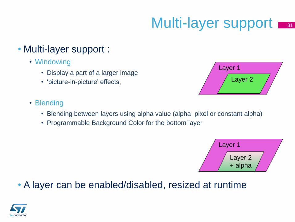
Multi-layer support
• Multi-layer support :
• Windowing
• Display a part of a larger image
• ‘picture-in-picture’ effects,
• Blending
• Blending between layers using alpha value (alpha pixel or constant alpha)
• Programmable Background Color for the bottom layer
• A layer can be enabled/disabled, resized at runtime
31
Layer 1
Layer 2
Layer 1
Layer 2
+ alpha

Graphic Acceleration
10/25/2013 Presentation Title
32

Introduction
• With the integration of LCD TFT controllers, graphical data generation
is consuming a lot of CPU
• To offload the CPU of raw data copy, a special DMA is needed to be
able to copy a part of a graphic content into another part of a graphic
content. Such an IP is usually called DMA 2D
• In addition to raw data copy, additional functionality can be added
such as image format conversion or image blending (image mixing
with some transparency).
33

Purpose of a Graphic Accelerator
• Independently from the mandatory refresh rate of the TFT panel
(60fps) the graphic content must be created in the frame buffer as fast
as possible
• The speed of the content creation can be translated in animation fps
• Have a TFT controller driving the display at 60fps means stable image and best
color rendering but does NOT mean fluent animations
• Fluency of animation or animation fps is directly linked with the graphical library, the
CPU performance and hardware graphic acceleration
• On MPUs graphic acceleration means Open GL / Open GL ES which
is far from the MCU world
• ST has developed a proprietary graphic accelerator in relationship
with MCU graphical library vendor to accelerate the most used low
level functions
• Direct management at graphical library low-level drivers
• Transparent migration from non accelerated product to accelerated product
• Best in class performances with CPU offload 10/25/2013 Presentation Title

Benefits
• Offload CPU from graphical data manipulation
• Master on the AHB bus matrix
• Speed up graphical content creation
• Perform rectangle to rectangle copy automatically
• Handled by low level drivers of the graphical library
• Option for image format conversion
• Option for image composition (blending of two sources)
• Speed up frame buffer updates
• Can update frame buffer without CPU
35

Typical data flow 36
BUS MATRIX
ARM
Cortex-M4
Core
DMA TFT
Controller
RAM FMC
DMA-2D
Flash APB
Creation of an object in a memory device by the DMA2D
Update of the frame buffer in the external RAM by the DMA2D
TFT controller data flow

Accelerated Features (1/2) 37
10/25/2013 Presentation Title
Feature Renesas NXP Freescale Microchip STM32
Rectangle filling (solid color) Partial
(with DMA)
Partial
(with GPDMA)
Yes
(with DMA) Yes Yes
Rectangle copy Partial
(with DMA)
Partial
(with GPDMA)
Yes
(with DMA) Yes Yes
Rectangle copy with Pixel Format Conversion No No No No Yes
Image composition (blending of 2 sources) No No No No Yes
• Some of the competitors can use their system DMA to accelerate few
features but none of them can do more than simple data copy
• DMA2D is totally independent from system DMA and has been designed
for graphical operations
• Thanks to its integrated pixel format converter and blender it accelerates
the most CPU consuming tasks

Accelerated Features (2/2)
• AHB bus master with burst access to any system memory
• Programmable rectangle size and rectangle address in the memory
• Programmable data format (from 4-bit indirect up to 32-bit direct)
• Dedicated memory for color lookup table (CLUT)
• Programmable address destination and format
• Optional image format conversion from direct or indirect color mode to
direct color mode
• Optional blending machine with programmable transparency factor
and/or with native transparency channel between to independent
image input to the destination image.
38
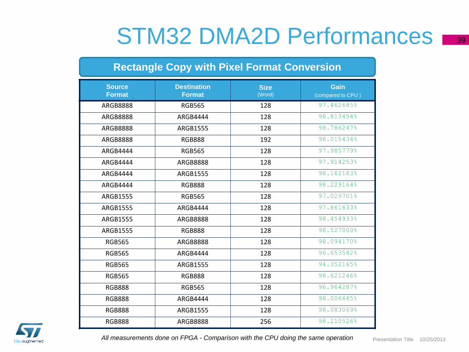
STM32 DMA2D Performances 39
10/25/2013 Presentation Title
Source
Format
Destination
Format Size
(Word)
Gain
(compared to CPU )
ARGB8888 RGB565 128 97.462685%
ARGB8888 ARGB4444 128 98.813454%
ARGB8888 ARGB1555 128 98.786247%
ARGB8888 RGB888 192 98.015434%
ARGB4444 RGB565 128 97.985779%
ARGB4444 ARGB8888 128 97.914253%
ARGB4444 ARGB1555 128 98.162163%
ARGB4444 RGB888 128 98.229164%
ARGB1555 RGB565 128 97.029701%
ARGB1555 ARGB4444 128 97.861633%
ARGB1555 ARGB8888 128 98.454933%
ARGB1555 RGB888 128 98.527000%
RGB565 ARGB8888 128 98.094170%
RGB565 ARGB4444 128 96.653542%
RGB565 ARGB1555 128 94.352165%
RGB565 RGB888 128 98.621246%
RGB888 RGB565 128 96.964287%
RGB888 ARGB4444 128 98.006645%
RGB888 ARGB1555 128 98.083069%
RGB888 ARGB8888 256 98.210526%
Rectangle Copy with Pixel Format Conversion
All measurements done on FPGA - Comparison with the CPU doing the same operation

DMA2D
Integration with Graphic Library 40
10/25/2013 Presentation Title
Cortex-M4
Segger emWin
Application
Cortex-M4
Segger emWin
Application
• DMA2D integration is transparent for the application
• The low-level drivers of the graphical stack are upgraded to directly use
DMA2D for data transfer, pixel format conversion and blending
• CPU load is decreased and graphical operations are faster

Implementation examples and
resources requirements
10/25/2013 STM32 Graphic
41

Single Chip MCU
• Internal Flash up to 2MB
• Internal SRAM up to 256KB
• Frame buffer in internal SRAM
• 16-bit QVGA (~150 KB)
• 8-bit WQVGA (~130 KB)
•Package LQFP 100pin
42
10/25/2013 STM32 Graphic
Bus Matrix
TFT
Controller Cortex-M4
Internal
Flash
Internal
SRAM
External
Memory
Controller
DMA2D
16-bit QVGA, 8-bit WQVGA
STM32F42x
Cost saving +
Graphic Acceleration
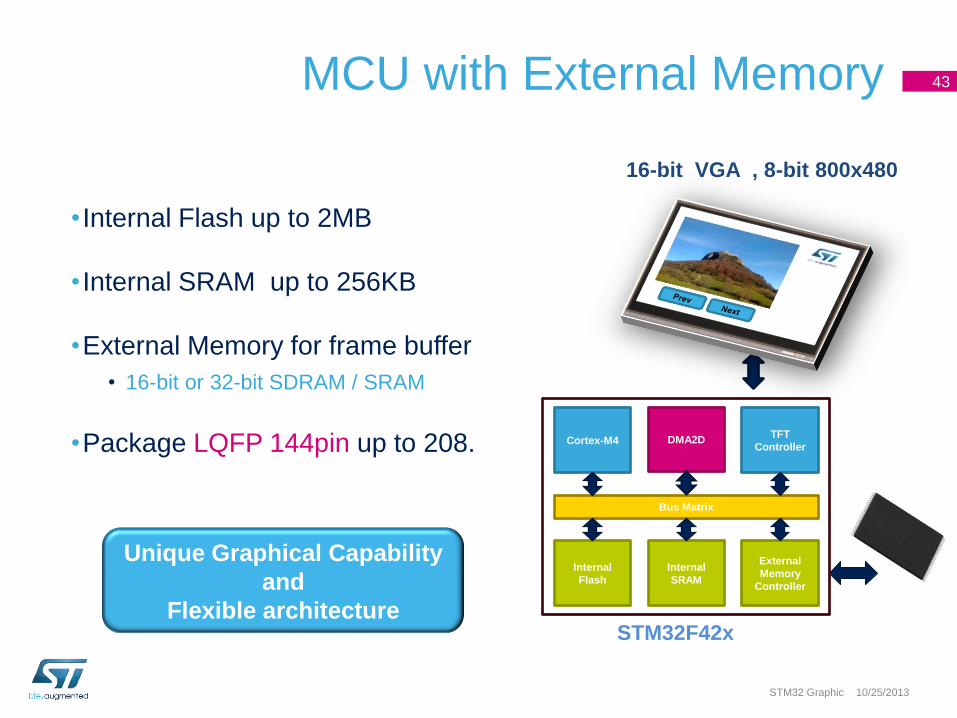
MCU with External Memory
• Internal Flash up to 2MB
• Internal SRAM up to 256KB
•External Memory for frame buffer
• 16-bit or 32-bit SDRAM / SRAM
•Package LQFP 144pin up to 208.
43
10/25/2013 STM32 Graphic
16-bit VGA , 8-bit 800x480
Bus Matrix
TFT
Controller Cortex-M4
Internal
Flash
Internal
SRAM
External
Memory
Controller
DMA2D
STM32F42x
Unique Graphical Capability
and
Flexible architecture

Frame buffer size & bandwidth (1/2)
Variant Display Size Color Depth Frame Buffer Bandwidth STM32F42x
package
High-end
7” Color TFT
800x480
(30MHz Pclk)
24-bit
(16.7M color) 1125kBytes 90MBytes/s
BGA176 /
LQFP176
16-bit
(262k color) 750kBytes 60MBytes/s
LQFP144/
BGA176 /
LQFP176
8-bit palletized
(256 / 16.7M color) 375kBytes 30MBytes/s
BGA176 /
LQFP176
Mid-range
2.5” Color TFT
400x240
(7.5MHz Pclk)
24-bit
(16.7M color) 281.25kBytes 22.5MBytes/s
BGA176 /
LQFP176
16-bit
(262k color) 187.5kBytes 15MBytes/s
LQFP144/
BGA176 /
LQFP176
Low-end
2.5” Mono
400x240
(7.5MHz Pclk)
96kBytes 93.75kBytes 7.5MBytes/s
LQFP100/
BGA176 /
LQFP176
VGA 640x480
(25MHz Pclk)
16-bit
(262k color) 600kBytes 50MBytes/s
BGA176 /
LQFP176
WQVGA 480x272
(9.5MHz Pclk)
24-bit
(16.7M color) 382.5kBytes 28.5MBytes/s
BGA176 /
LQFP176
Dedicated Graphic RAM needed 10/25/2013 STM32 Graphic
44

Frame buffer size & bandwidth (2/2) STM32 Graphic
Variant Display Size Color Depth Frame Buffer Bandwidth STM32F42x
package
WQVGA 480x272
(9.5MHz Pclk)
8-bit palletized
(256 / 16.7M color)
127.5KBytes
30MBytes/s
LQFP100/
LQFP144/
BGA176 /
LQFP176
QVGA
5.7” Color TFT
320x240
(6.4 MHz Pclk)
16-bit
(262k color) 150kBytes 12.8MBytes/s
LQFP100/
LQFP144/
BGA176 /
LQFP176
8-bit palletized
(256 / 16.7M color) 75kBytes 6.4MBytes/s
LQFP100/
LQFP144/
BGA176 /
LQFP176
10/25/2013
45

Variant - High-End
• STM32F4-2MB + External Memory
• 16-bit VGA , 8-bit WVGA
• 16-bit or 32-bit SDRAM / SRAM
• Package: LQFP144, LQFP176/ BGA176 or LQFP208/BGA216
10/25/2013
Bus Matrix
TFT
Controller Cortex-M4
Internal
Flash
Internal
SRAM
External
Memory
Controller
DMA2D
STM32F42x STM32 Graphic
46

Variant - Mid-range
10/25/2013
• STM32F4-2MB + External Memory for frame buffer
• 24-bit WQVGA
• Needs between 400~600kBytes of RAM for graphics
• Package : LQFP144, LQFP176/BGA176 or LQFP208/BGA216
Bus Matrix
TFT
Controller Cortex-M4
Internal
Flash
Internal
SRAM
External
Memory
Controller
DMA2D
STM32F42x STM32 Graphic
47

Variant - Low-end – Option1
10/25/2013
• STM32F4-2MB + Internal Memory for frame buffer
• 16-bit QVGA, 8-bit WQVGA
• Mid-Range option without external RAM.
• Package : LQFP100 /LQFP144
Bus Matrix
TFT
Controller Cortex-M4
Internal
Flash
Internal
SRAM
External
Memory
Controller
DMA2D
STM32F42x STM32 Graphic
48

Variant - Low-end – Option2
• STM32F1/4x + TFT with embedded controller & GRAM
• Package : LQFP100 /LQFP144
Bus Matrix
Cortex-M
Internal
Flash
Internal
SRAM
External
Memory
Controller
10/25/2013 STM32 Graphic
49
DMA2D TFT
Controller
DMA2D and TFT controller available on STM32F4+2MB

Which package to use depending on the
variant targeted?
10/25/2013
Variant TFT Controller + External
Frame Buffer
External Memory Interface
SDRAM STM32F42x package
Hig-End Yes
16-bit LQFP144/
BGA176 / LQFP176
32-bit
LQFP208/BGA216
Mid-End Yes
16-bit LQFP144/
BGA176 / LQFP176
32-bit LQFP208/BGA216
Low-End No No LQFP100
SDRAM devices example: • MT48LC4M16A2P-7E : 64Mb
• MT48LC16M16A2P-7E : 256Mb
STM32 Graphic
50
SDRAM Controller
First Technical Slides
NEW
Benefits
• Grant more RAM resources for user application
• Accessible by all AHB masters
• Dedicated Read Data Cache
• Code execution from SDRAM
52

SDRAM main features (1/4)
• Up to 512MB continues memory range split into two banks, can be seen as a single
device.
53
SDRAM Bank1
256MB (4x16MBx32-bit)
256MB (4x16MBx32-bit)
SDRAM Bank2
FMC SDRAM
Up to 512MB
Independent chip select
Independent configuration
Easy to use
0xC000 0000
0xDFFF FFFF

SDRAM main features (2/4)
• Fully programmable SDRAM interface:
• Configurable SDRAM clock speed :
• Half speed (HCLK /2),
• One-third speed (HCLK /3)
• Timing parameters for different SDRAM devices requirements
• CAS latency of 1,2,3
• Memory data bus width : 8-bit, 16-bit and 32-bit
• Up to 4 internal banks with configurable Row and Column sizes :
• up to 13-bits Address Row,
• up to 11-bits Address Column.
54

SDRAM main features (3/4)
• Optimized initialization sequence:
• The initialization command sequence can be executed simultaneously for the two banks.
Initialization time can be divided by 2.
• Remap of SDRAM Space
• Option1: Remap at adress 0x0
• Option2: SDRAM space swap with NAND Bank3 and PCCard
• Energy-saving: two low power modes are supported:
• Self-refresh Mode
• Power-down Mode
55
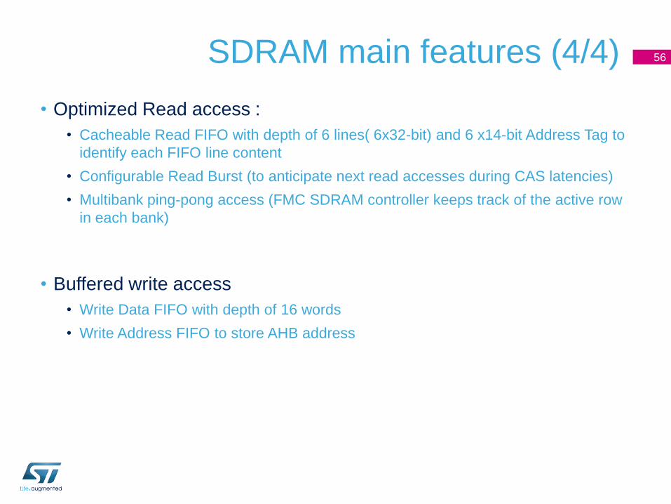
SDRAM main features (4/4)
• Optimized Read access :
• Cacheable Read FIFO with depth of 6 lines( 6x32-bit) and 6 x14-bit Address Tag to
identify each FIFO line content
• Configurable Read Burst (to anticipate next read accesses during CAS latencies)
• Multibank ping-pong access (FMC SDRAM controller keeps track of the active row
in each bank)
• Buffered write access
• Write Data FIFO with depth of 16 words
• Write Address FIFO to store AHB address
56

Read Data Cache access (1/2) 57
AHB Master Read request at @0x00
Data_0 at @0x00
@0x04 Data_1
@0x08 Data_2
Anticipated read
during CAS latency
FMC SDRAM Controller
6 lines
FIFO
Read FIFO Addr. TAG
SDRAM
device
(CAS = 3)
Request response
AHB Master
request

Read Data Cache access (2/2) 58
AHB Master Read request at @0x04
Data_1 at @0x04
@0x04 Data_1
@0x08 Data_2
FMC SDRAM Controller
6 lines
FIFO
Address TAG available in Read
FIFO
Read FIFO Addr. TAG
SDRAM
device
(CAS = 2)
Request response
AHB Master
request

Application example
• Memory-intensive applications
• Graphical application (e.g Multi-frame display)
• Multimedia application
• Download/run programs to/from external SDRAM
59

Linux like application (µClinux) 60
Applications
µClinux OS
Hardware (STM32 + SDRAM)

Ability to store large amounts of raw data
61
FMC
DMA
DCMI
Camera
Ethernet
DMA
Data streaming from
high speed peripherals

Crypto/Hash

Cryptographic processor (CRYP)

64
Definitions
• Plaintext is the original text/values to be encrypted; the original message.
• Encryption is the process used to convert plaintext into a form that is not readable without knowledge of the rules and key to decrypt.
• Decryption is the process used to convert from an encrypted form back to plaintext, using a key.
• A key is the value string used for both encryption and decryption.
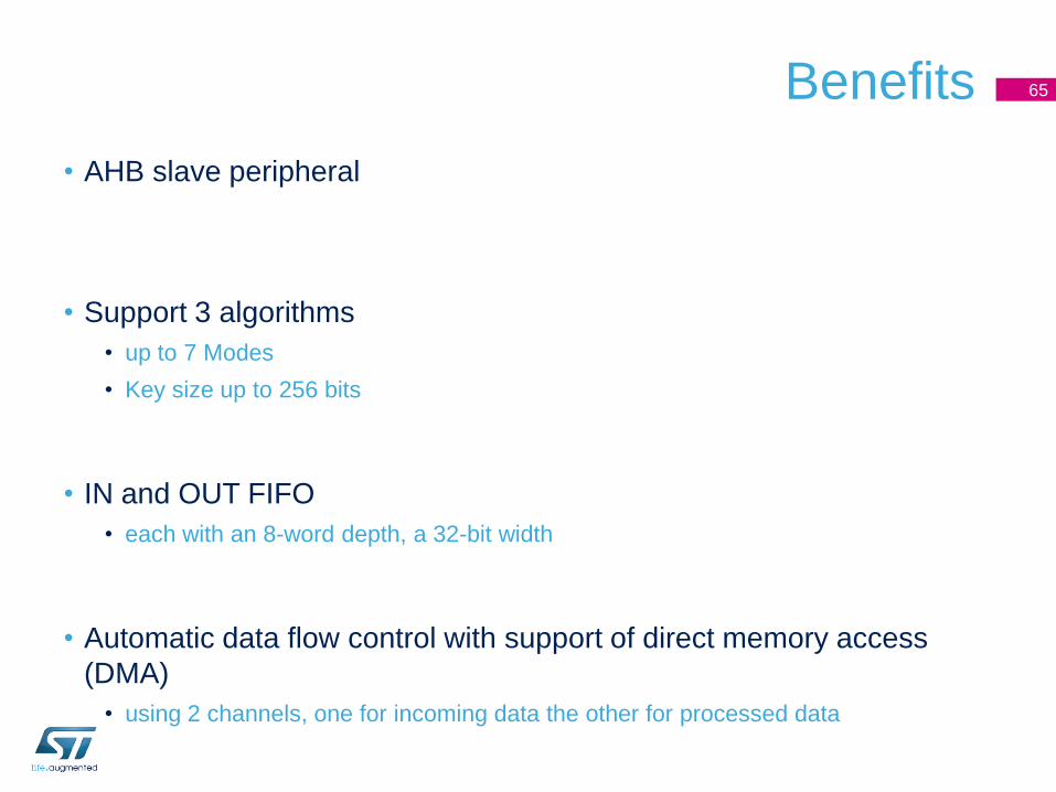
Benefits
• AHB slave peripheral
• Support 3 algorithms
• up to 7 Modes
• Key size up to 256 bits
• IN and OUT FIFO
• each with an 8-word depth, a 32-bit width
• Automatic data flow control with support of direct memory access
(DMA)
• using 2 channels, one for incoming data the other for processed data
65
66
CRYP algorithms principle AES : Advanced Encryption Standard
DES : Data Encryption Standard
TDES : Triple Data Encryption Standard
Sender
Clear
Data
Encrypted
Data Cipher
Symmetric
key
Receiver
Clear
Data
Encrypted
Data DeCipher
Symmetric
key

67
Encryption/ Decryption Modes
Electronic code book(ECB),
Cipher block chaining(CBC) and
Counter(CTR) modes.
GCM: AES Galois/Counter Mode
CCM: Combined Cipher Machine
Two other Modes are dberived form the new modes:
GMAC: Galois Message Authentication Code
CMAC: Cipher Message Authentication Code
allows encryption and
authentication
allows
authentication only
Allows encryption only .

68
CRYP algorithms overview
AES DES TDES
Key sizes 128, 192 or 256 bits 64* bits
* 8 parity bits
192***, 128** or 64* bits * 8 parity bits : Keying option 1
** 16 parity bits: Keying option 2
***24 parity bits: Keying option 3
Block sizes 128 bits 64 bits 64 bits
Time to process
one block
14 HCLK cycle for key = 128bits
16 HCLK cycle for key = 192bits
18 HCLK cycle for key = 256bits
16 HCLK cycles 48 HCLK cycles
Type block cipher block cipher block cipher
Structure Substitution-permutation
network Feistel network Feistel network
First published 1998 1977 (standardized
on January 1979) 1998 (ANS X9.52)

69
CRYP Block Diagram
Key: 128-, 192- and 256-bit
Key: 64-bit
Key: 64-, 128- and 192-bit
TDES
AES
DES
CRYPTO Processor
Inp
ut
FIF
O
Ou
tpu
t F
IFO
Data
sw
ap
pin
g
Data
sw
ap
pin
g
ECB CBC CTR DMA request
for incoming
data transfer
DMA request
for outgoing
data transfer
ECB CBC
ECB CBC
GCM CCM
New Encryption/ Decryption Modes
Interruption Routine

Hash processor (HASH)

Definitions • A cryptographic hash function is the transformation of a message
into message digest with usually shorter fixed-length value that
depend of Hash algorithm applied.
Message
(data to be encoded)
arbitrary block of data
fixed-size bit string
Digest Hash function
71
MD5: message digest size is 128bits
SHA-1: message digest size is 160 bits
SHA-224: message digest size is 224 bits
SHA-256: message digest size is 256bits
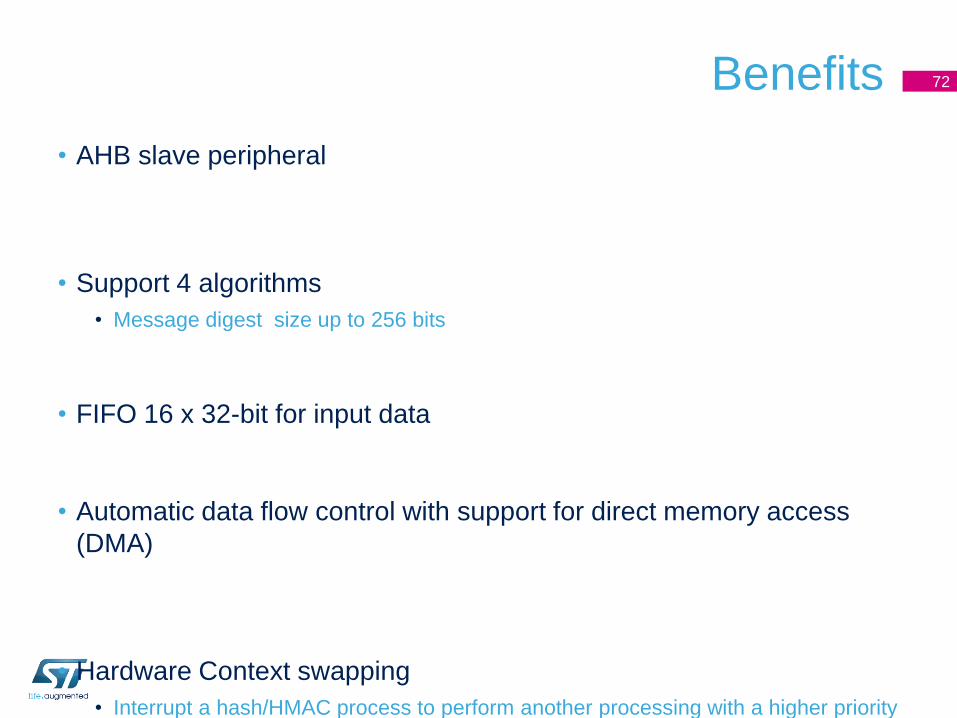
Benefits
• AHB slave peripheral
• Support 4 algorithms
• Message digest size up to 256 bits
• FIFO 16 x 32-bit for input data
• Automatic data flow control with support for direct memory access
(DMA)
• Hardware Context swapping
• Interrupt a hash/HMAC process to perform another processing with a higher priority
72

HASH Block Diagram
MD5 SHA-1
HASH
HASH Processor
Inp
ut
FIF
O
Data
sw
ap
pin
g
DMA request
HMAC
Message
Digest
H0..H7
8x32bit 16 x
32b
it
73
SHA-224 SHA-256
Interruption routine
New Hash algorithms

HMAC operation • The HMAC algorithm is used for message authentication, by irreversibly
binding the message being processed to a key chosen by the user.
• For HMAC specifications, refer to “HMAC: keyed-hashing for message authentication, H. Krawczyk, M. Bellare, R. Canetti, February 1997.
• Basically, the algorithm consists of two nested hash operations:
pad
key
Concat
0x5C
concat
message
HASH HMAC Concat
HASH
0x36
74

SAI - Serial Audio Interface
First Technical Slides
NEW

SAI Introduction
76
The SAI interface (Serial Audio Interface) is a
new peripheral supporting a wide set of audio
protocols thanks to its flexible architecture

SAI benefits
• Modular architecture many stereo or mono audio applications may be
targeted:
• I2S standards (SAI= 2xI2S half duplex or 1xI2S full duplex),
• LSB or MSB-justified,
• PCM with “DSP” mode support
• TDM (Time Division Multiplex) Allows multiple connections (DACs, Bluetooth
chip…) over the bus
• AC’97
• SPDIF output
77

SAI Features
Two independent audio sub-blocks which can be
Transmitter and/or receiver
Master or slave
Synchronous or asynchronous mode between the audio sub-blocks
Clock generator for each audio block to target independent audio frequency
sampling
8-word integrated FIFOs for each audio sub-block.
Data size configurable : 8-bit, 10-bit, 16-bit, 20-bit, 24-bit, 32-bit
DMA interface with 2 dedicated channels to handle the access to the dedicated
Up to 16 slots available with configurable size and with the possibility to select
which ones are actives in the audio frame.
Mute mode.
Stereo/Mono audio frame capability.
78

WS_B SCK_B SD_B MCLK_B
SAI Top Level Architecture 79
WS_A SCK_A SD_A MCLK_A
FIFO
8x32b
Clo
ck
ge
ne
rato
r fo
r
Ma
ste
r c
on
fig
ura
tio
n
BLOC A
BLOC B
Clock1
Clock2
CKin
PLL
SysCK
FIFO
8x32b
STM32F4xx
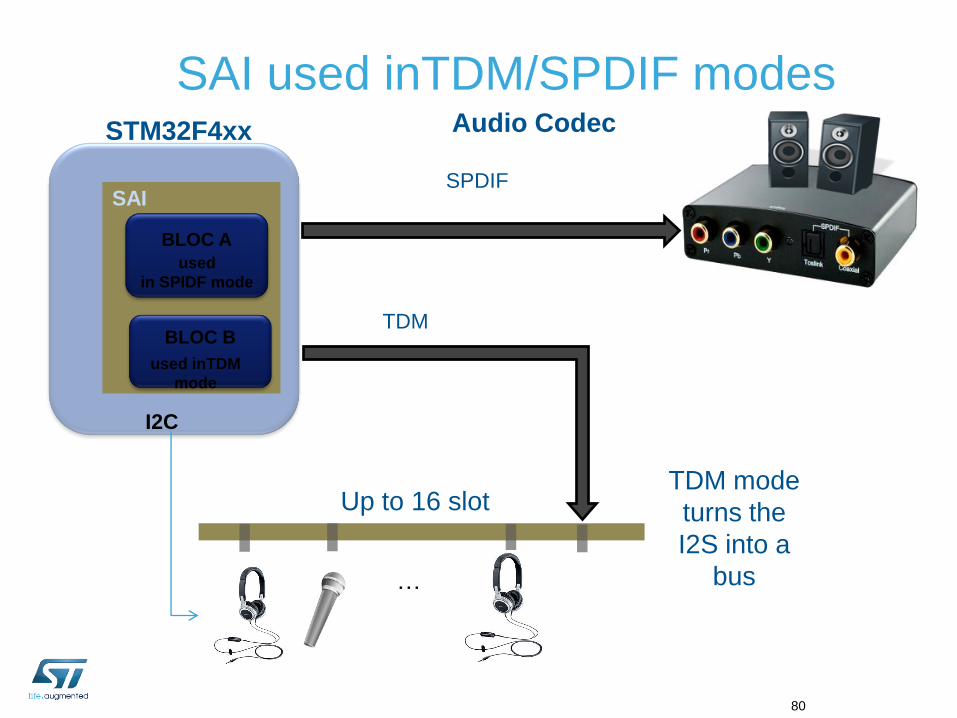
SAI used inTDM/SPDIF modes
80
…
Up to 16 slot
BLOC A
BLOC B
used inTDM
mode
used
in SPIDF mode
Audio Codec STM32F4xx
SAI
I2C
TDM mode
turns the
I2S into a
bus
SPDIF
TDM

SAI used in I2S Full-Duplex mode
CK
SDIn
WS
MCLK
I2C controls *
Audio Codec
An
alo
g In
terf
ac
e
Dig
ita
l In
terf
ac
e
STM32F4xx
CK
SDout
WS
MCLK
SDout SDIn
81
+
I2S
SAI


![Modular Connected [2MB]](https://img.pdfslide.net/doc/110x75/58a2f86c1a28ab8e608c1e28/modular-connected-2mb.jpg)