Embed Size (px)
Citation preview

April 2006 Rev 1 1/27
AN2317Application Note
STPM01 Programmable, Single-PhaseEnergy Metering IC External Circuits
IntroductionThe STPM01 is implemented in an advanced 0.35µm BCD6 technology. It is designed for active, reactive, and apparent energy measurement, including Root Mean Square (VRMS and I RMS), instantaneous, and harmonic voltage and current.
This application note describes the STPM01 external circuits which are comprised of:
● a crystal oscillator,
● a power supply circuit,
● a voltage sensing circuit, and
● two current sensing circuits.
Note: This document should be used in conjunction with the STPM01 datasheet.
www.st.com

Contents AN2317 - Application
2/27
Contents
1 External Circuit Design . . . . . . . . . . . . . . . . . . . . . . . . . . . . . . . . . . . . . . . 4
1.1 Current Sensing Circuit . . . . . . . . . . . . . . . . . . . . . . . . . . . . . . . . . . . . . . . 6
1.1.1 Primary Current Sensing . . . . . . . . . . . . . . . . . . . . . . . . . . . . . . . . . . . . . 6
1.1.2 Secondary current sensing . . . . . . . . . . . . . . . . . . . . . . . . . . . . . . . . . . . 9
1.2 Anti-aliasing Filter . . . . . . . . . . . . . . . . . . . . . . . . . . . . . . . . . . . . . . . . . . . 11
1.3 Voltage Sensing Circuit . . . . . . . . . . . . . . . . . . . . . . . . . . . . . . . . . . . . . . 15
1.4 Crosstalk Cancellation Network . . . . . . . . . . . . . . . . . . . . . . . . . . . . . . . . 17
1.5 Capacitive Power Supply Circuit . . . . . . . . . . . . . . . . . . . . . . . . . . . . . . . 18
1.5.1 Varistor . . . . . . . . . . . . . . . . . . . . . . . . . . . . . . . . . . . . . . . . . . . . . . . . . . 18
1.5.2 Capacitive Power Supply . . . . . . . . . . . . . . . . . . . . . . . . . . . . . . . . . . . . 19
1.5.3 EMC Filter . . . . . . . . . . . . . . . . . . . . . . . . . . . . . . . . . . . . . . . . . . . . . . . 22
1.6 Clock Generation . . . . . . . . . . . . . . . . . . . . . . . . . . . . . . . . . . . . . . . . . . . 24
2 Revision History . . . . . . . . . . . . . . . . . . . . . . . . . . . . . . . . . . . . . . . . . . . 26

AN2317 - Application List of Figures
3/27
List of Figures
Figure 1. STPM01 External Circuit Schematics . . . . . . . . . . . . . . . . . . . . . . . . . . . . . . . . . . . . . . . . . . 5Figure 2. Primary Current Sensing Circuit . . . . . . . . . . . . . . . . . . . . . . . . . . . . . . . . . . . . . . . . . . . . . . 6Figure 3. Current Sense Transformer-to-Power Line Connections . . . . . . . . . . . . . . . . . . . . . . . . . . . 8Figure 4. Shunt Module-to-Power Line Connections . . . . . . . . . . . . . . . . . . . . . . . . . . . . . . . . . . . . . 10Figure 5. Anti-aliasing Filter . . . . . . . . . . . . . . . . . . . . . . . . . . . . . . . . . . . . . . . . . . . . . . . . . . . . . . . . 11Figure 6. Anti-aliasing Effect . . . . . . . . . . . . . . . . . . . . . . . . . . . . . . . . . . . . . . . . . . . . . . . . . . . . . . . 11Figure 7. Anti-aliasing Filter Magnitude Response . . . . . . . . . . . . . . . . . . . . . . . . . . . . . . . . . . . . . . 14Figure 8. Anti-aliasing Filter Phase Response . . . . . . . . . . . . . . . . . . . . . . . . . . . . . . . . . . . . . . . . . . 14Figure 9. Voltage Sensing Circuit . . . . . . . . . . . . . . . . . . . . . . . . . . . . . . . . . . . . . . . . . . . . . . . . . . . 15Figure 10. Crosstalk Network. . . . . . . . . . . . . . . . . . . . . . . . . . . . . . . . . . . . . . . . . . . . . . . . . . . . . . . . 17Figure 11. Capacitive power supply (with EMC Filter) . . . . . . . . . . . . . . . . . . . . . . . . . . . . . . . . . . . . . 18Figure 12. Capacitive Power Supply . . . . . . . . . . . . . . . . . . . . . . . . . . . . . . . . . . . . . . . . . . . . . . . . . . 19Figure 13. Internal RC Recommended Connections . . . . . . . . . . . . . . . . . . . . . . . . . . . . . . . . . . . . . . 24Figure 14. Quartz Recommended Connections. . . . . . . . . . . . . . . . . . . . . . . . . . . . . . . . . . . . . . . . . . 24Figure 15. External Clock Source Recommended Connections . . . . . . . . . . . . . . . . . . . . . . . . . . . . . 25

External Circuit Design AN2317 - Application
4/27
1 External Circuit Design
Figure 1 on page 5 shows an implementation example of the STPM01 in a simple Stepper Counter Connector design. The main external circuits include:
● a Current Sensing Circuit,
● an Anti-aliasing Filter on page 11,
● a Voltage Sensing Circuit on page 15,
● a Capacitive Power Supply Circuit on page 18, and
● a Clock Generation on page 24 (RC oscillator, quartz, or external clock).

AN2317 - Application External Circuit Design
5/27
Figure 1. STPM01 External Circuit Schematics
10
9
7
8
6
5
4
2
1
20
9
7
5
3
1
11
12
13
14
16
17
15
3
18
19
10
8
6
4
2
IIP2
IIN2
VIP
VIN
CLKIN
CLKOUT
SYN
SCS
SCL
SDA
IIN1
IIP1
VOIP
VDDA
VCC
VSS
VDD
MOP
MON
LED
1 2
1 2 1 2 1 2
1 2
2
1
2
1
2
1
1 2
4 1
2
1
12
1
1
2
1
2
1
2
1
2
2
1
2
1
2
12 1
2 1
1
1
2
1
2
1
2
1
2
11
31 23
1
2
2 2
1
12 12 12 12
2
2 2 1
2
1
1 1 2
VDD
VDD
PIG08 10-2V
C5
C4
R5
E46
22/X
503
C6
1MY
C7
1MY
30.1
R
R1
1.0k
R13
2M
R2
TR1
1.0k
1MY
C8
10N
R20
U1STPM01E
2.4K
R19
2.4K
R18
2.4K
R17
2.4K1.
0N
1.0N
1.0N C3
C2
D1
D6
SR
D 2
00m
cdD
10
DIF
60
D12
5.6V
D11
DIF60
D7
SR
D 2
00m
cd
D8
SR
D 2
00m
cd
D9
SR
D 2
00m
cd
1N41
48
D2
1N4148
D3
1N4148
D4
1N4148
D5
1N4148
VDDA
VDD
SBGSDASCLSCSSYN
VDDA
C12
15P
C13
15P
C16
1MY
C17
10N
C18
10N
C19
10N
R23
47K
R15
1M
Y1
4194.304kHz
R21
Q3
BC
8578
Q4BC8578
W5VODNIK
W6VODNIK33
.0R
R22 1K
1 2C11
4.7my
C20
220NC1
470N
1 2C10
10N
1 2R14
2M
1
1
W3VODNIK
F
N
W4VODNIK
L6
L3
220MYH
220MYH
1
1
W1VODNIK
W2VODNIK
1 2 1 2
1 2
4 1
2
1
R6
E46
22/X
503
30.1
R
R4
1.0k
R3
TR2
1.0k
C9
10N
1 2
1
1
2
1
2
1
2 1
2
1
2
1
2
2 1 2 1 2
1 2
1 2
R8
261K
R24
82R
1 2R9
261K
1 2R10
261K
1 2R7
475R
1 2R11
150K
1 2R12
2.21k
C15
+
1000
M
C14
1.0NV4
510V
AI12296
CAPACITIVE POWER SUPPLY
VOLTAGE SENSING
ANTI-ALIASING FILTER
CRYSTAL OR RTCOSCILLATOR
CURRENT SENSING

External Circuit Design AN2317 - Application
6/27
1.1 Current Sensing CircuitThe STPM01 has two external current sensing circuits (see Figure 1 on page 5):
1. Primary channel, and
2. Secondary channel.
1.1.1 Primary Current Sensing
The primary channel uses a current transformer to couple the mains current (see Figure 2).
The Burden resistor is used to produce a voltage between VIN1 and VIP1. The Low-pass filter (LPF) is used to filter out the high frequency interference and has little influence on the voltage drop between VIN1 and VIP1.
Figure 2. Primary Current Sensing Circuit
2 1 2
1 2
1
2
1
R25
6.8R
R1
1.0k
R2I2
VIN1
VIP1
U0
+
–
Burden Resistor LPFI1
1.0k
C9
10N
2
1
R23 1R
AI12297

AN2317 - Application External Circuit Design
7/27
Primary current sensing is calculated as follows:
Equation 1
Equation 2
Assuming I1PEAK, the calculation will proceed as:
Equation 3
Equation 4
Equation 5
The maximum differential input voltage between VIN1 and VIP1 is dependent on the Programmable Gain Amplifier (PGA) selection. For the purposes of this application, use 8x as the gain value, then U0PEAK = 0.15V.
Equation 6
Equation 7
Equation 8
Equation 9
I2N1
N2------- I1⋅=
U0 UA I2R23 R25⋅R23 R25+--------------------------------⋅
N1N2-------- I1
R23 R25⋅R23 R25+--------------------------------⋅ ⋅==≈
I1PEAK
I2PEAK------------------
N2
N1-------= 2000
1-------------=
I2PEAKI1PEAK
2000------------------ 3mA==
U0PEAK UAPEAK I2PEAK
R23 R25⋅R23 R25+--------------------------⋅ 2.6mV===
UAPEAK U0PEAK 0.15V==
I2PEAK UAPEAK
R23 R25+
R23 R25⋅--------------------------⋅ 172mA==
I1PEAK 2000I2PEAK 344A==
I1RMS
I1PEAK
2------------------ 243A==

External Circuit Design AN2317 - Application
8/27
The primary current sensing circuit can be connected to mains as follows (see Figure 3):
1. The hot line voltage wire must be connected to pin F of the module.
Normally, this wire is also connected to the hot line current wire. However, during production or to verify phases, this wire may be connected to some other line voltage source.
2. The neutral line voltage wire must be connected to pin N of the module.
This wire is also connected to the neutral line current wire.
3. The hot line current wire must be placed through the current transformer TR1 hole (becoming the hot load wire).
Use insulated 4mm2 copper wire.
4. The neutral line current wire must be placed through the current transformer TR2 hole.
Use insulated 4mm2 copper wire.
Figure 3. Current Sense Transformer-to-Power Line Connections
AI12298
Neutral Load
Hot Load
Neutral Line
Hot Line
P1
W6
Comp side
TR2 TR1
*
F N
W5

AN2317 - Application External Circuit Design
9/27
1.1.2 Secondary current sensing
The secondary channel uses shunt resistor structure (see Figure 4). The 420µW shunt resistor is used to maximize the use of the dynamic range of the current sensing circuit. However, there are some important considerations when selecting a shunt structure for energy metering applications.
● The power dissipation in the shunt must be minimized.
The maximum rated current for this design element is 20A, so the maximum power dissipated in the shunt is calculated as follows:
● The higher power dissipation may make it difficult to manage the thermal issues.
Although the shunt is manufactured from manganin material, which is an alloy with a low thermal resistance, an apparent error may occur when it reaches a high temperature.
● The shunt should be able to resist the shortage of the phase circuit.
This reduces the shunt resistance is much as possible.
The design values used are:
– Mains voltage = 220VRMS,
– Ib = 2A, and
– Shunt resistance = 420µΩ.
The remaining design elements calculated from these values are as follows:
– Voltage across shunt:
– Mains power dissipation:
– Error:
20A( )2420μΩ 168mW=×
2A 420μΩ 0.00084V=×
220V 2A 0.44kW=×
1.68 103–× 0.44 10
3–× 100percent 0.0004percent=×⁄

External Circuit Design AN2317 - Application
10/27
The secondary current sensing circuit can be connected to the mains as shown in Figure 4:
1. The hot line voltage wire must be connected to pin N of the module.
Normally, this wire is also connected to the hot line current wire. However, during production or to verify phases, this wire may be connected to some other line voltage source.
2. The neutral line voltage wire must be connected to pin F of the module.
This wire is also connected to the neutral line current wire, which passes by the module.
3. The hot line current wire must be connected to the Shunt pole which is close to pin N of the module.
Use insulated 4mm2 copper wire.
4. The hot load current wire must be connected to the Shunt pole which is close to the edge of the module.
Use insulated 4mm2 copper wire.
Figure 4. Shunt Module-to-Power Line Connections
AI12299
Hot Load
Neutral
Hot Line
P1
W6
Comp side
Shunt
*
F N
W5LEDNLCTPRDIR

AN2317 - Application External Circuit Design
11/27
1.2 Anti-aliasing FilterThe anti-aliasing filter (Figure 5) is a low-pass filter. It reduces high frequency levels which may cause distortion due to the sampling (aliasing) that occurs before the analog inputs of an analog-to-digital converter (ADC) are introduced into the application (see Figure 6). Filtering is easily implemented with a resistor-capacitor (RC) single-pole circuit which obtains an attenuation of –20dB/dec.
Figure 5. Anti-aliasing Filter
Figure 6. Anti-aliasing Effect
R
R
UO
UI
C
C
AI12900
0 2 450 900
Frequency - kHz
ImageFrequencies
AI12901

External Circuit Design AN2317 - Application
12/27
The anti-aliasing filter magnitude and phase response can be calculated as follows:
Equation 10
Note: The cutoff frequency is expressed as:
So Equation 10 can be changed to:
Equation 11
Equation 12
The phase is expressed as:
Equation 13
In the module:
R = 2 • 103KΩ and
C = 10nF, so then
AuUO
UI
--------
1jωc---------
R 1jωc---------+
-------------------- 11 jωRC+-------------------------= = =
fp1
2πτ--------- 1
2πRC----------------= =
Au1
1 jffp----⋅+
-------------------- 1
1 jffp----⋅+
--------------------= =
Au1
1ffp----⎝ ⎠⎛ ⎞ 2
+
----------------------=
ϕ arc– ffp----tan=
fp1
2πRC---------------- 7961.8Hz= =

AN2317 - Application External Circuit Design
13/27
According to Equation 12 and Equation 13 on page 12, the filter’s magnitude and phase response can be seen in Figure 7 and Figure 8 on page 14.
● When f = 50Hz:
Equation 14
and
Equation 15
● When f = 60Hz:
Equation 16
and
Equation 17
Assume that the current lags the voltage by a phase angle, δ. After an anti-aliasing filter, a phase error (ϕ) is introduced into the STPM01. The power factor (PF) error is calculated as:
Equation 18
When,
δ = –60° (PF = –0.5), and
f = 50Hz,
according to Equation 14, a phase error, ϕ = –0.35° has occurred:
Equation 19
This indicates that even a small phase error will translate into a significant measurement error at a low power factor. Thus correct phase matching is required in this situation.
ϕ 0.35°–=
Au 1≈
ϕ 0.43°–=
Au 1≈
errorPFδcos δ ϕ+( )cos–
δcos----------------------------------------------- 100percent⋅=
errorPF60– °( )cos 60°– 0.35°–( )cos–
60– °( )cos---------------------------------------------------------------------------------- 100percent 1percent=⋅=

External Circuit Design AN2317 - Application
14/27
Figure 7. Anti-aliasing Filter Magnitude Response
Figure 8. Anti-aliasing Filter Phase Response
Frequency (Hz)1000 10000 100000 100000010010
–60
–40
–20
AI12902
0
Dec
ibel
s (d
B)
–100
AI12903
–40
–20
0
–80
–60
1000 10000 100000 100000010010Frequency (Hz)
Deg
rees
(°)

AN2317 - Application External Circuit Design
15/27
1.3 Voltage Sensing CircuitThe STPM01 normally uses a resistor divider as voltage input channel (see Figure 9). The 783kΩ resistor is separated into three 261kΩ, in-series resistors (see Figure 1 on page 5), which ensure that a high voltage transient will not bypass the resistor. These three resistors also reduce the potential across the resistors, thereby decreasing the possibility of arcing.
The following resistors are used as the resistor divider when the mains voltage is present:
● R‘ = 783KΩ, and
● R5=475Ω.
C11 and (R19+ R15) create a filter which prevents Electromagnetic Interference (EMI) created by the circuit from migrating onto the Line or Neutral busses (see Equation 20 through Equation 24 on page 16).
Figure 9. Voltage Sensing Circuit
R1942.2k
R'
783k
R'V1
V2
L21m
Z2Z1
783k
C1122n
R15100
R5475
R6475
AI12904

External Circuit Design AN2317 - Application
16/27
Equation 20
Equation 21
Equation 22
Equation 23
Z1 has little influence on the U0, thus:
Equation 24
Note: For a specific U0, choose an appropriate combination of resistors (R5 and R’) to get that particular U0 value.
Z1 R19 R15+( ) 42.3KΩ= =
Z2R5 R6+( ) Z1⋅R5 R6 Z1+ +------------------------------------ 930Ω= =
U1 U2–
Z2
2------
2R ′ Z2+---------------------- Vmains
Vmains 110 2V U1 0.046V=,=
Vmains 220 2V U1 0.092V=,=⎩⎪⎨⎪⎧
=⋅= =
U0 U1 U2–
Z2
2------
R′Z2
2-------+
------------------- VmainsVmains 110 2V U0 0.092V=,=
Vmains 220 2V U0 0.185V=,=⎩⎪⎨⎪⎧
=⋅= =
U0
R5
R′ R5+-------------------≈

AN2317 - Application External Circuit Design
17/27
1.4 Crosstalk Cancellation NetworkThe voltage front end handles voltages of considerable amplitude, which makes it a potential source of noise. Disturbances are readily emitted into current measurement circuitry where it will interfere with the actual signal to be measured. Typically, this shows as a non-linear error at small signal amplitudes and non-unity power factors.
At unity power factor, voltage and current signals are in phase and crosstalk between voltage and current channels merely appears as a gain error, which can be calibrated. When voltage and current are not in phase, crosstalk will have a non-linear effect on the measurements, which cannot be calibrated.
Crosstalk is minimized by means of good PCB planning and the proper use of filter components in the crosstalk network. Recommended filter components are shown in Figure 10. The network subtracts a signal proportional to the voltage input from the current input. This prevents crosstalking within the STPM01. The signal subtraction is calculated in Equation 25 and Equation 26.
Equation 25
Equation 26
Note: This network must be applied to every STPM01 design, from the voltage channel to each current channel.
Figure 10. Crosstalk Network
VR15R15
R19 R15+----------------------------- VVCI
R15R19----------- VVCI⋅≅⋅=
VCCIR1
R21 R1+------------------------- VR15
R1R21----------- VR15⋅≅⋅ R1
R21----------- R15
R19----------- VVCI 1.18e
6–VVCI≅⋅ ⋅= =
R1942.2k
–
+
VVCIVoltage
ChannelInput
VCCICurrentChannelInput
+
–
R15100
R11k
R21
2M
AI12908

External Circuit Design AN2317 - Application
18/27
1.5 Capacitive Power Supply CircuitThe capacitive power supply circuit is shown in Figure 10 and includes:
● a varistor,
● the capacitive power supply, and
● the Electromagnetic Compatibility (EMC) filter.
Figure 11. Capacitive power supply (with EMC Filter)
1.5.1 Varistor
The varistor is a surge protection device that is connected directly across the AC input. When a power surge or voltage spike exceeding a specified voltage (varistor voltage) is sensed, the varistor's resistance rapidly decreases, creating an instant shunt path for the overvoltage, thereby saving the sensitive control panel components. The varistor and the line fuse are subject to damage or weakened because the shunt path creates a short circuit.
An essential point of varistor selection is that the varistor can handle the peak pulse current, which is 110% of the maximum current at which the varistor voltage does not change. If the peak pulse current rating is insufficient, then the varistor may be damaged. The main voltage is 220VRMS, and sometimes the maximum will reach 265VRMS.Thus, an MOKS K10*300V varistor is chosen for this application.
VDD
TransientProtection
CurrentLimiter
VoltageDividerFilter 1 Filter 2
GND
C11n
D35.1V
RV1510V
D2DIF60
D1
DIF60LINE
NEUTRAL
AI12909
1
2
R1
82R
L1220m
L2220m
C31000m
C2
470n

AN2317 - Application External Circuit Design
19/27
1.5.2 Capacitive Power Supply
There are several ways to convert AC voltage into the DC voltage required by STPM01. Traditionally, this is done with a transformer and rectifier circuit. There is also switching power supply solution. However, these two solutions are expensive and take up a considerable amount of PCB space.
To provide a low-cost, alternative solution, a transformerless power supply can be used (see Figure 12).
Figure 12. Capacitive Power Supply
VDD
UIN
IIN
GND
D35.1V
D2DIF60
D1
DIF60LINE
NEUTRAL
AI12914
1
2
R1
82R
C31000m
C2
470n

External Circuit Design AN2317 - Application
20/27
The input current (IIN) is limited by R1 and the capacitive reactance of C2 (see Equation 28 and Equation 29), and is expressed as:
Equation 27
where,
XC2 = C2 reactance.
Note: R1 is used to limit inrush current, but it dissipates power.
By adding a low-cost half-wave rectifier, current is allowed to be supplied by the source during the positive half, where,
● VINRMS = RMS voltage of the half-wave AC waveform, and is expressed as follows:
Equation 28
where,
VPEAK = mains peak voltage (i.e. United States = 115V/60Hz and Europe = 220V/50Hz), and
VZ = the voltage drop across D1 and D3.
● XC2 = Capacitor reactance, and is expressed as:
Equation 29
By substituting the values expressed in Equation 27 with those in Equation 28 and Equation 29, the results are as follows:
Equation 30
Assuming that the voltage drop across each diode is 0.7V, then the total voltage drop is expressed as:
Equation 31
IINVIN RMS( )XC2 R1+-------------------------=
VIN RMS( )12---
VPEAK VZ–
2-------------------------------⋅=
XC21
2π fC2----------------=
IINVPEAK VZ–
2 2 XC2 R1+( )----------------------------------------
2Vmains VZ–
2 2 XC2 R1+( )----------------------------------------= =
VZ VD1 VD3 5 0.7 2 6.4V=⋅+=+=

AN2317 - Application External Circuit Design
21/27
When these application parameters are considered:
Vmains = 220VAC,
f = 50Hz, and
VZ = 6.4V (see Equation 31), the calculated IIN would be:
Equation 32
Selecting components in the circuit is a critical consideration. As a general rule, components should be sized at twice the maximum power calculated for each device.
For example, by using the IIN value in Equation 32 and VDD = 5V to choose an appropriate Zener diode, the results required to make the selection are expressed as follows:
Equation 33
and
Equation 34
Thus, a ZMM SOD 80*5.1V G Zener Diode is used.
IIN 15.7mA=
VDD IIN2
R1 0.02W=⋅=
PD3 VD3 IIN 5.1 0.0157 0.08W=⋅=⋅=
External Circuit Design AN2317 - Application
22/27
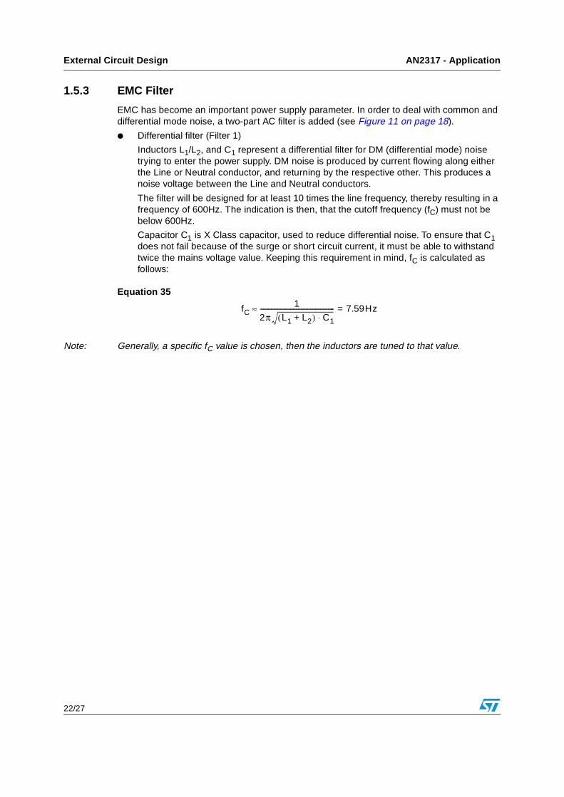
1.5.3 EMC Filter
EMC has become an important power supply parameter. In order to deal with common and differential mode noise, a two-part AC filter is added (see Figure 11 on page 18).
● Differential filter (Filter 1)
Inductors L1/L2, and C1 represent a differential filter for DM (differential mode) noise trying to enter the power supply. DM noise is produced by current flowing along either the Line or Neutral conductor, and returning by the respective other. This produces a noise voltage between the Line and Neutral conductors.
The filter will be designed for at least 10 times the line frequency, thereby resulting in a frequency of 600Hz. The indication is then, that the cutoff frequency (fC) must not be below 600Hz.
Capacitor C1 is X Class capacitor, used to reduce differential noise. To ensure that C1 does not fail because of the surge or short circuit current, it must be able to withstand twice the mains voltage value. Keeping this requirement in mind, fC is calculated as follows:
Equation 35
Note: Generally, a specific fC value is chosen, then the inductors are tuned to that value.
fC1
2π L1 L2+( ) C1⋅----------------------------------------------- 7.59Hz=≈

AN2317 - Application External Circuit Design
23/27
● Capacitor filter (C3, Filter 2)
Capacitor C3 is used as a filter. Considering load RL, the size of C3 must satisfy the requirements expressed in Equation 36:
Equation 36
In fact, considering that the charge stored in the capacitor is:
Equation 37
where,
IL = the load current, and
T = the AC sine wave period, and
the output ripple voltage is expressed as:
Equation 38
then the capacitor C value can be calculated by using a fixed voltage ripple value:
Equation 39
then, fixing our ripple to ΔV=200mV we can calculate C value accordingly.
For the purposes of this application, C is calculated as follows:
Equation 40
The STPM01 power supply (VCC) configuration range is from 3.3V to 6V. While it seems to be enough to change the D3 diode (see Equation 34) from the previously selected ZMM SOD 80*5.1V G Zener Diode, if the output current is too high, then the C2 value must be reduced.
Note: Usually it is not necessary to use resistor R1 in the circuit.
RLC 15 25∼( )T=
ILT Q=
ΔV QC----=
ΔVILT
C--------=
C 10mA200mV 50Hz⋅-------------------------------------- 1000μF= =

External Circuit Design AN2317 - Application
24/27
1.6 Clock GenerationAll of the STPM01 internal timing is based on the CLKOUT oscillation signal. This signal can be generated in three different ways:
● RC (see Figure 13)
This oscillator mode can be selected using the RC configuration bit. If RC = 1, then the STPM01 will run using the RC oscillator. A resistor connected between CLKIN and Ground will set the RC current.
Note: For 4MHz operation, the suggested settling resistor is 12k.
● Quartz (see Figure 14)
The oscillator will work with an external crystal.
Figure 13. Internal RC Recommended Connections
Figure 14. Quartz Recommended Connections
VSS
12k
CLKIN CLKOUT
AI12915
VSS
1M
4194MHz15pF15pF
CLKIN CLKOUT
AI12916

AN2317 - Application External Circuit Design
25/27
● External Clock (see Figure 15)
The clock generator is powered from analog supply, and is responsible for two tasks:
a) to retard the turning on of some of the function blocks after Power-on Reset (POR) in order to help smooth start the external power supply circuitry and keep all major loads off of the circuit, and
b) to provide all necessary clocks for the analog and digital parts. Two nominal frequency ranges are expected,(1) from 4.000MHz to 4.194MHz, or (2) from 8.000MHz to 8.192MHz.
Figure 15. External Clock Source Recommended Connections
VSS
–
CLKIN CLKOUT
AI12917

Revision History AN2317 - Application
26/27
2 Revision History
Table 1. Document revision history
Date Revision Changes
14-Apr-2006 1 Initial release.

AN2317 - Application
27/27
Please Read Carefully:
Information in this document is provided solely in connection with ST products. STMicroelectronics NV and its subsidiaries (“ST”) reserve theright to make changes, corrections, modifications or improvements, to this document, and the products and services described herein at anytime, without notice.
All ST products are sold pursuant to ST’s terms and conditions of sale.
Purchasers are solely responsible for the choice, selection and use of the ST products and services described herein, and ST assumes noliability whatsoever relating to the choice, selection or use of the ST products and services described herein.
No license, express or implied, by estoppel or otherwise, to any intellectual property rights is granted under this document. If any part of thisdocument refers to any third party products or services it shall not be deemed a license grant by ST for the use of such third party productsor services, or any intellectual property contained therein or considered as a warranty covering the use in any manner whatsoever of suchthird party products or services or any intellectual property contained therein.
UNLESS OTHERWISE SET FORTH IN ST’S TERMS AND CONDITIONS OF SALE ST DISCLAIMS ANY EXPRESS OR IMPLIEDWARRANTY WITH RESPECT TO THE USE AND/OR SALE OF ST PRODUCTS INCLUDING WITHOUT LIMITATION IMPLIEDWARRANTIES OF MERCHANTABILITY, FITNESS FOR A PARTICULAR PURPOSE (AND THEIR EQUIVALENTS UNDER THE LAWSOF ANY JURISDICTION), OR INFRINGEMENT OF ANY PATENT, COPYRIGHT OR OTHER INTELLECTUAL PROPERTY RIGHT.
UNLESS EXPRESSLY APPROVED IN WRITING BY AN AUTHORIZE REPRESENTATIVE OF ST, ST PRODUCTS ARE NOT DESIGNED,AUTHORIZED OR WARRANTED FOR USE IN MILITARY, AIR CRAFT, SPACE, LIFE SAVING, OR LIFE SUSTAINING APPLICATIONS,NOR IN PRODUCTS OR SYSTEMS, WHERE FAILURE OR MALFUNCTION MAY RESULT IN PERSONAL INJURY, DEATH, ORSEVERE PROPERTY OR ENVIRONMENTAL DAMAGE.
Resale of ST products with provisions different from the statements and/or technical features set forth in this document shall immediately voidany warranty granted by ST for the ST product or service described herein and shall not create or extend in any manner whatsoever, anyliability of ST.
ST and the ST logo are trademarks or registered trademarks of ST in various countries.
Information in this document supersedes and replaces all information previously supplied.
The ST logo is a registered trademark of STMicroelectronics. All other names are the property of their respective owners.
© 2006 STMicroelectronics - All rights reserved
STMicroelectronics group of companies
Australia - Belgium - Brazil - Canada - China - Czech Republic - Finland - France - Germany - Hong Kong - India - Israel - Italy - Japan - Malaysia - Malta - Morocco - Singapore - Spain - Sweden - Switzerland - United Kingdom - United States of America
www.st.com