Embed Size (px)
Citation preview
Strain and Charge Co-Mediated Magnetoelectric Coupling in Thin Film Multiferroic Heterostructures
A Thesis Presented by
Xinjun Wang To
The Department of Electrical and Computer Engineering
in partial fulfillment of the requirements for the
degree of
Master of Science in the
field of
Electrical Engineering
Northeastern University
Boston, Massachusetts
October, 2014
1
Acknowledgments
I would like to thank my advisor Professor Nian-Xiang Sun, for his
support and patient guidance on my research career. His creativity,
sensitivity and enthusiasm to research inspired me. I wish I can achieve
further research goals with his guidance in the pursuit of my doctoral
degree.
I would like to thank Professor Yongming Liu and Professor Marvin
Onabajo for being on my committee. Their advices to my thesis are
invaluable.
I would like to thank my colleagues Dr. Satoru Emori, Dr. Zhongqiang
Hu, Dr. Zhiguang Wang, Dr. Ziyao Zhou, Yuan Gao, Tianxiang Nan,
Whyder Lin, Xie Li etc. for their help and suggestion to my research.
Finally, I would like to show my great gratitude to my family for their
unconditional love and meticulous support on my life.
2
Contents
List of Figures .................................................................................................................... 5
Chapter 1. Introduction to artificial multiferroic heterostructure and ferroelectricity .. 11
1.1 Multiferroic and magnetoelectric materials .......................................................................... 11
1.2 Electric field control of magnetism in magnetoelectric composite ................................................... 15
1.2.1. Strain-mediated magnetoelectric effect ............................................................. 15
1.2.2. Charge-mediated magnetoelectric effect ........................................................... 19
1.2.3. Exchange-bias mediated magnetoelectric effect ................................................ 21
1.2.4. Strain and charge co-mediated magnetoelectric coupling ................................. 22
Chapter 2: Fabrication and Characterization ................................................................ 24
2.1. Metallic magnetic thin film fabrication: physical vapor deposition system (PVD) .................... 24
2.2. Ferroelectric characterization .......................................................................................................... 27
2.3. Static magnetic property characterization: vibration sample magnetometer (VSM) .................. 28
2.4 Introduction to Electron Paramagnetic Resonance (EPR) .............................................................. 29
Chapter 3. Voltage Control of Magnetism in FeGaB/ PIN-PMN-PT Heterostructures 32
3.1. Introduction ....................................................................................................................................... 32
3.2 Experiment ......................................................................................................................................... 33
3.3 Results and discussion ....................................................................................................................... 34
3.4. Conclusion ......................................................................................................................................... 43
3
Chapter 4. E-tuning of FMR in ultrathin NiFe/PLZT heterostructures .......................... 44
4.1 Introduction ........................................................................................................................................ 44
4.2 Experiment ......................................................................................................................................... 47
4.3 Results and Discussion ...................................................................................................................... 48
4.4 Conclusion .......................................................................................................................................... 57
Chapter 5. Low temperature fabricated multiferroics heterostructure ........................... 58
5.1. Introduction ....................................................................................................................................... 58
5.2. Experiment ........................................................................................................................................ 59
5.3. Results and discussions ..................................................................................................................... 59
5.4 Conclusion .......................................................................................................................................... 72
Chapter. 6 Conclusion and future plan ........................................................................... 73
6.1. Conclusion ......................................................................................................................................... 73
6.2. Future Plan ....................................................................................................................................... 74
6.2.1. Co-existence of strain and charge mediated magnetoelectric coupling for non- volatile control of magnetism ........................................................................... 74
6.2.2. Power Efficient Tunable Inductors for RFIC .................................................... 75
Reference ......................................................................................................................... 77
4
List of Figures
Figure 1.1 (a) Relationship between multiferroic and magnetoelectric materials. Illustrates
the requirements to achieve both in a material (b) Schematic illustrating different types of
coupling present in materials. Much attention has been given to materials where electric
and magnetic order is coupled. These materials are known as magnetoelectric
materials……………………………………………………………………………………………………………………………………….10
Figure 1.2 Electric field dependence of the in-plane field-sweep FMR spectra of the
FeGaB/PZN-PT multiferroic heterostructure measured at ca. 9.6 GHz………………………..16
Fig 1.3 (a) FMR fields of NiFe/Cu/PMN-PT(011) and (b) NiFe/PMN-PT(011) upon applying different
electric fields with the bias magnetic field applied along the in-plane [0–11] direction. Insets show
schematic of NiFe/PMN-PT heterostructure (up) with strain and surface charge at the interface and
NiFe/Cu/PMN-PT heterostructure with only strain at the interface(down)…………………………………….23
Figure 2.1 Schematic of Magnetron sputtering…………………………………………………………………26
Figure 2.2 Radient Precision LC ferroelectric test system………………………………………………..28
Figure 2.3 The LakeShore 7407 VSM………………………………………………………………………………29
Figure 2.4 the schematic of measured theory………………………………………………………………….30
Figure 2.5 EPR measure system…………………………………………………………………………………….31
Fig.3.1 Polarization and piezoelectric strain of (011) oriented PIN-PMN-PT as a function of
electric field, where the electric coercive field was found at ±6.7 kV/cm……………………….36
Fig. 3.2 (a) Magnetic hysteresis loops of FeGaB/PIN-PMN-PT heterostructures measured at
5

various electric field; (b) Magnetization ratio at a low magnetic bias field (i.e., 5 Oe) as a
function of E-field…………………………………………………………………………………38
Fig. 3.2 (a) Magnetic hysteresis loops of FeGaB/PIN-PMN-PT heterostructures measured at
various electric field; (b) Magnetization ratio at a low magnetic bias field (i.e., 5 Oe) as a
function of E-field.…………………………………………………………………………………..39
Fig.3. 4(a) FMR spectra of FeGaB/PIN-PMN-PT at various E-field with external magnetic
fields along [01-1] direction; (b) effective magnetic field as a function of E-field for [100] and
[01-1] directions……………………………………………………………………………………40
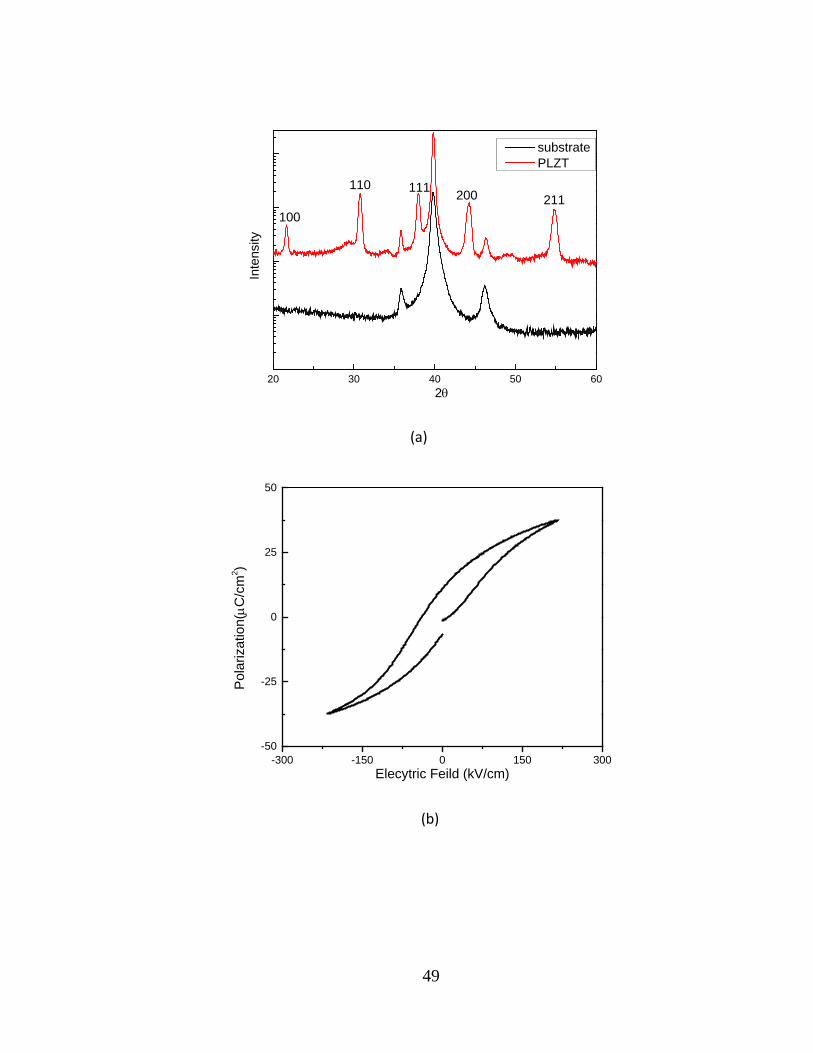
Fig 4.1 (a) X-ray diffraction pattern of the RF sputtered STO/Pt multilayer on Si substrate; (b)
P-E hysteresis loops PLZT films; (c) AFM image of PLZT surface with calibrated roughness of
1.5nm……………………………………………………………………………………………….50
Fig. 4.2. (a) Schematic of the sample used for a voltage-induced FMR field change. A schematic
of multilayer structure of Cu/NiFe/PLZT/Pt/Si. The magnetic field was applied perpendicular to
the film plane for FMR measurements; (b) voltage dependence of the in-plane field-sweep FMR
spectra of the NiFe/PLZT multiferroic heterostructure measured at 9.5 GHz. The zero cross
part was enlarged to demonstrate a clear ME coupling shift at bottom left inset………………52
Figure 4.3 (a) FMR of NiFe with different thickness (b) the relative between the thickness of
NiFe and effective field…………………………………………………………………………………..54
Figure 4.4 (a) FMR of NiFe with 1.5nm thickness by applying voltage from -15V to 15V; (b)
Relative between PLZT polarization and magnetic field changes; (c) FMR of NiFe with 1.5nm
6
thickness by applying voltage from -7V to 7V; (d) Relative between PLZT polarization and
magnetic field changes……………………………………………………………………………56
Figure 5.1(a) XRD pattern of NiZn ferrite thin film pH(P)=4.6, pH(O)=9.6, precursor
concentration of 10ML; (b) SEM image of NiZn ferrite thin film, pH(P)=4.6, pH(O)=9.6,
precursor concentration of 10ML; (c) Grain size of NiZn ferrite film dependence of growth
conditions; (d) AFM image of NiZn ferrite thin film, pH(P)=4.6, pH(O)=9.6, precursor
concentration of 10ML…………………………………………………………………………………………….63
Figure 5.2 (a) M-H loops of varying pH(P) at fixed pH(O) and precursor concentration; (b) M-
H loops of varying pH(O) at fixed pH(P) and precursor concentration; (c) M-H loops of varying
precursor concentration at fixed pH(P) and pH(O); (d) Hc, Mr, Magnetization at 100Oe
dependence of pH(P); (e) Hc, Mr, Magnetization at 100Oe dependence of pH(O); (f) Hc, Mr,
Magnetization at 100Oe dependence of precursor concentration………………………………66
Figure 5.3 (a) FMR spectrums of varying pH(P) at fixed pH(O) and precursor concentration;
(b) FMR spectrums of varying pH(O) at fixed pH(P) and precursor concentration; (c) FMR
spectrums of varying precursor concentration at fixed pH(P) and pH(O); (d) FMR linewidth
dependence of pH(P), pH(O) and precursor concentration……………………………………..71
Figure 5.4 (a) Permeability spectrum of NiZn thin film with pH(P)=4.6, pH(O)=9.6 and
precursor concentration of 10ML; (b) Permeability at 0.5 GHz of varying pH(P), pH(O) and
precursor concentration; (c) Resistivity of NiZn films at varying pH(P), pH(O) and precursor
concentration
…………………………………………………………………………………………………………..70
7
Abstract
Recently, more and more researching has been focused on multiferroic materials and
devices due to the demonstrated strong magnetoelectric coupling in new multiferroic
materials, artificial multiferroic heterostructures and devices with unique
functionalities and superior performance characteristics. This has resulted in
opportunities for us to achieve compact, fast, energy efficient and voltage tunable
spintronic devices. Traditionally, i n magnetic materials based magnetic random access
memories (MRAM) devices, magnetization is used to store the binary information.
Since the high coercivity of the ferromagnetic media requires high magnetic fields for
switching the magnetic states, so it needs large amount of energy.
A spin torque technique that is used in Modern MRAM information writing processes
minimizes the large energy for generating a magnetic field by passing through a spin-
polarized current directly to the magnets. However, this two methods still consumes a lot
of energy because of the large current or current density requirement to toggle the
magnetic bits. Many papers reports that spin is controlled by the electrical field which
supplies new opportunities for power efficient voltage control of magnetization in
spintronic devices for magnetoeletric random use for memories (MERAM) with ultra-low
energy consumption. However, state of the art multiferroic materials still make it chatting
to realize non-volatile 180 magnetization reversal, which is desired in realizing MERAM.
8
In a strain-mediated multiferroic system, the typical modification of the magnetism
of ferromagnetic phase as a function of bipolar electric field shows a “butterfly” like
behavior. This is due to the linear piezoelectricity of ferroelectric phase which has a
“butterfly” like piezostrain as a function of electric field curve resulting from
ferroelectric domain wall switching. Compared with charge-mediated
multiferroic, the strain-mediated multiferroic system needs much higher
voltage than charge-mediated, because of the thickness of ferroelectric is
different. In a strain-mediated multiferroic system, the substrate is bulk
materials and in a charge-mediated multiferroic system, the substrate is a
thin film on dielectric material.
In this work, we study the equivalence of direct and converse
magnetoelectric effects. The resonant direct and converse magnetoelectric (ME)
effects have been investigated experimentally. For a strain-mediated multiferroic system,
we use PIN-PMN-PT, PMN-PT as the substrate. LFO, YIG, FeGaB are used as the
magnetic thin film to study the tubability. This linear piezoelectric effect in converse
magnetoelectric coupling would lead to “butter-fly” like magnetization vs. electric field
curve which leads to a “volatile” behavior in magnetic memory system. In a charge-
mediated system, we use NiFe/PLZT/Si to study the tunability. The frequency responses
of direct and converse magnetoelectric effects were measured under the same electric and 9
magnetic bias conditions. In this study, VSM and FMR are studies in different situation.
Furthermore, we studied the low temperature fabricated multiferroic heterostructure, to
find out the best solution to get the thin film by spin spray. Different PH and temperature
are used. VSM and FMR were employed to measure properties of thin film. XRD and
SEM were used to analyse the composition and surface.
10
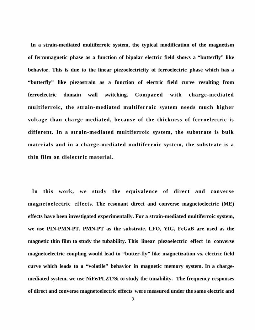
Chapter 1. Introduction to artificial multiferroic heterostructure and ferroelectricity
1.1 Multiferroic and magnetoelectric materials
Recently, more and more research has found on multiferroic materials because
of its large potential for applications in novel electronic devices1-8. Multiferroic materials are
the group of at least two ferroic properties in one system, with the ferroic properties including
ferroelectric, (anti-) ferromagnetism and ferroelastic. Strong magnetoelectric coupling could
be induced due to the strong coupling interaction between two ferroic orders9. As shown in
Figure 1.1 (a) multiferroic materials require two or all three of the properties
ferroelectricity, ferromagnetism, and ferroelasticity occur in the same phase10
.
There are two different kinds of magnetoelectric coupling. O n e i s called driect
magnetoelectric coupling, the other is called converse magnetoelectric coupling. For the direct
magnetoelectric coupling, there is an appearance of an electric polarization upon the
application of a magnetic field. In this case, the magnetic field applied on the multiferroic
material is capable of modifying the electric polarization of that material. Also, an electric
potential or a voltage output can be induced by the applied alternating magnetic field which
may lead to high resolution magnetic field sensor applications11-15
. Symmetrically, the
converse magnetoelectric response is the existence of magnetization upon the application of
11
electric field. This means the modification of magnetic property by an electric field which
provides great opportunities in the voltage control of spintronics, reconfigurable electronics
and tunable microwave devices with ultra-low energy consumption16-21.
Figure 1.1 (a) Relationship between multiferroic and magnetoelectric materials.
Illustrates the requirements to achieve both in a material (b) Schematic illustrating
different types of coupling present in materials. Much attention has been given to
materials where electric and magnetic order is coupled. These materials are known as
magnetoelectric materials10
.
From the materials point of view, the multiferroic materials can be classified to single-
phase and artificial composite multiferroics or magnetoelectrics. The multiferroic effect
has been observed as an intrinsic effect in some natural material systems such as BiFeO3
and some rare earth manganates6, 22-24. However, the single-phase multiferroic materials
which have low Curie temperature or weak magnetoelectric coupling coefficient may 12
be impractical to real device applications25,26. On the other hand, the artificial multiferroic
or magnetoelectric composites formed by combing ferroelectric and ferromagnetic phases
show strong ME coupling with several orders of magnitude higher ME coupling
coefficients compared to single phase multiferroics8. The strong ME coupling realized
in multiferroic materials enables effective energy conversion between electric and
magnetic fields, and has led to many different multiferroic devices from magnetic
sensors, voltage tunable RF/microwave signal processing devices, spintronics, etc.
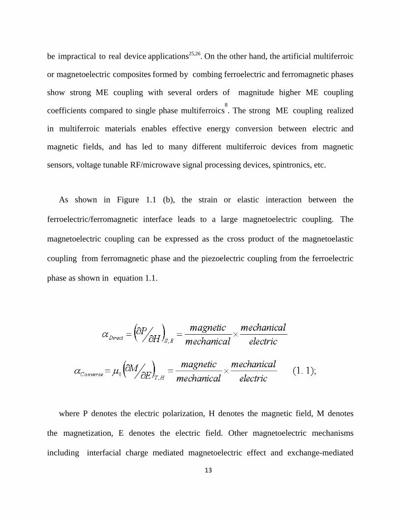
As shown in Figure 1.1 (b), the strain or elastic interaction between the
ferroelectric/ferromagnetic interface leads to a large magnetoelectric coupling. The
magnetoelectric coupling can be expressed as the cross product of the magnetoelastic
coupling from ferromagnetic phase and the piezoelectric coupling from the ferroelectric
phase as shown in equation 1.1.
where P denotes the electric polarization, H denotes the magnetic field, M denotes
the magnetization, E denotes the electric field. Other magnetoelectric mechanisms
including interfacial charge mediated magnetoelectric effect and exchange-mediated
13
magnetoelectric coupling also show great capability in modifying the magnetism by
electric field. In multiferroic composites, both ferromagnetic and ferroelectric phases can
be selected separately to meet the devices design principles. For example, high quality
microwave ferrite/ferroelectric heterostructures have been demonstrated for tunable
RF/microwave devices19,27; ultra-thin magnetic thin film/dielectric thin film utilizing the
charge-mediated magnetoelectric effect has been realized for voltage controlled magnetic
tunnel junction.28-30
14
1.2 Electric field control of magnetism in magnetoelectric composite
1.2.1. Strain-mediated magnetoelectric effect Strain-mediated magnetoelectric coupling is one of the main approaches for the electric field
control of magnetism8. Due to the converse piezoelectric effect from the ferroelectric phase,
an external strain can be generated. That strain transfers to the ferromagnetic phase through
the interface, which finally modifies the magnetism of ferromagnetic phase due to the
magnetoelastic coupling. Strain mediated magnetoelectric (ME) coupling in layered
ferromagnetic/ferroelectric heterostructures provides great opportunities in realizing novel
multiferroic devices such as magnetoelectric random access memories (MERAMs)31-33
.
Through phase field simulations, Hu and coworkers demonstrated a new approach towards
voltage- controlled magnetic random access memory (MRAM) through strain mediated
magnetoelectric coupling in magnetic tunneling junction on a ferroelectric layer
heterostructure32
. Strain mediated magnetoelectric coupling can lead to a 90ᵒ rotation of the
in-plane magnetization of the free layer in the magnetic tunneling junctions. Simulation
results show that these voltage- controlled MRAM devices have ultra-low writing energy
(less than 0.16 fJ per bit), room temperature operation, high storage density, good thermal
stability and fast writing speed. This mechanism has been achieved in the 1-3 type
ferromagnetic BFO and ferroelectric CFO vertical heterostructure film34
. The CFO
nanopillars are embedded into the BFO film with an intimate lattice coupling between this 15
two ferroic phases in nanoscale. The magnetoelectric coupling was evidently proved by the
MFM images, where the magnetic property of CFO was altered by the applied electric field
on the BFO film.
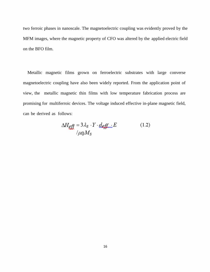
Metallic magnetic films grown on ferroelectric substrates with large converse
magnetoelectric coupling have also been widely reported. From the application point of
view, the metallic magnetic thin films with low temperature fabrication process are
promising for multiferroic devices. The voltage induced effective in-plane magnetic field,
can be derived as follows:
16
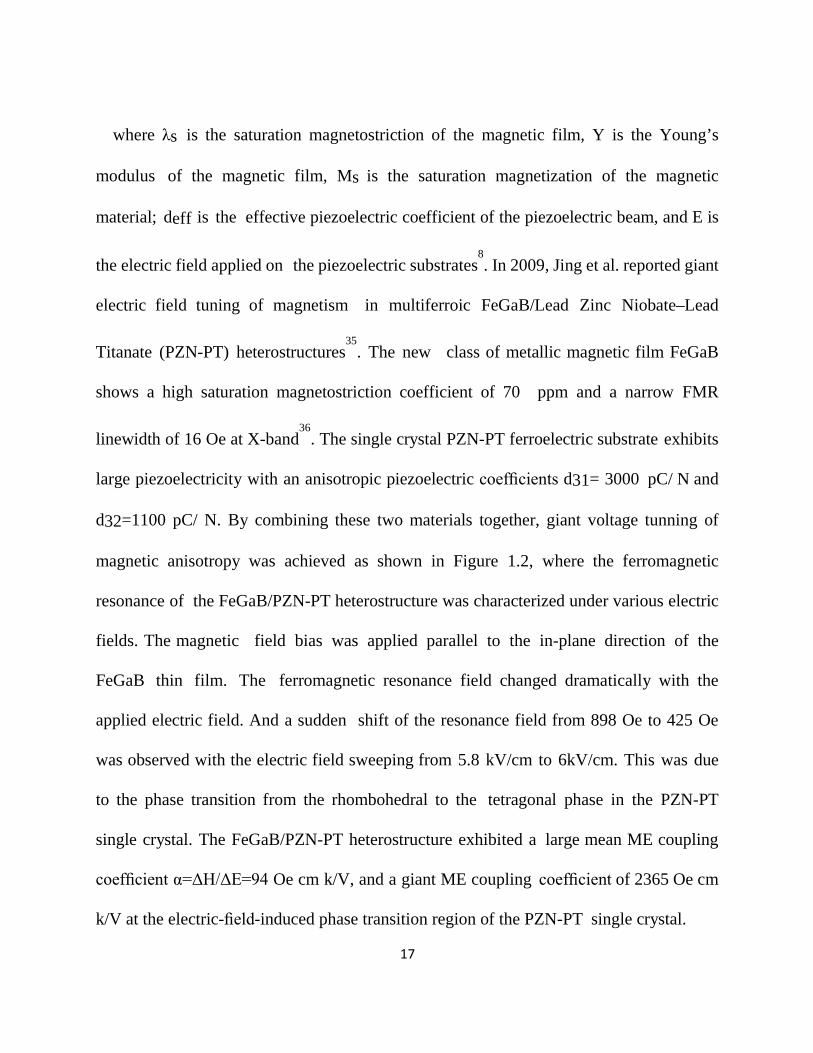
where λs is the saturation magnetostriction of the magnetic film, Y is the Young’s
modulus of the magnetic film, Ms is the saturation magnetization of the magnetic
material; deff is the effective piezoelectric coefficient of the piezoelectric beam, and E is
the electric field applied on the piezoelectric substrates8. In 2009, Jing et al. reported giant
electric field tuning of magnetism in multiferroic FeGaB/Lead Zinc Niobate–Lead
Titanate (PZN-PT) heterostructures35
. The new class of metallic magnetic film FeGaB
shows a high saturation magnetostriction coefficient of 70 ppm and a narrow FMR
linewidth of 16 Oe at X-band36
. The single crystal PZN-PT ferroelectric substrate exhibits
large piezoelectricity with an anisotropic piezoelectric coefficients d31= 3000 pC/ N and
d32=1100 pC/ N. By combining these two materials together, giant voltage tunning of
magnetic anisotropy was achieved as shown in Figure 1.2, where the ferromagnetic
resonance of the FeGaB/PZN-PT heterostructure was characterized under various electric
fields. The magnetic field bias was applied parallel to the in-plane direction of the
FeGaB thin film. The ferromagnetic resonance field changed dramatically with the
applied electric field. And a sudden shift of the resonance field from 898 Oe to 425 Oe
was observed with the electric field sweeping from 5.8 kV/cm to 6kV/cm. This was due
to the phase transition from the rhombohedral to the tetragonal phase in the PZN-PT
single crystal. The FeGaB/PZN-PT heterostructure exhibited a large mean ME coupling
coefficient α=ΔH/ΔE=94 Oe cm k/V, and a giant ME coupling coefficient of 2365 Oe cm
k/V at the electric-field-induced phase transition region of the PZN-PT single crystal.
17
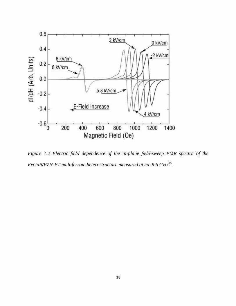
Figure 1.2 Electric field dependence of the in-plane field-sweep FMR spectra of the
FeGaB/PZN-PT multiferroic heterostructure measured at ca. 9.6 GHz35.
18
1.2.2. Charge-mediated magnetoelectric effect
The charge mediated magnetoelectric effect was first reported by Weisheit et al.
describing that the magnetocrystalline anisotropy of ultra-thin iron-platinum and iron-
palladium magnetic layer can be reversibly controlled by electric field in an
electrolyte37. The screening charge provided by liquid electrolyte modified the intrinsic
magnetic properties. This direct way of voltage control of magnetism offers an
opportunity for electric field induced resistance change in magnetic tunnel junctions,
the core portion of MRAM devices. Maruyama et al29. also reported the change of
magnetic anisotropy in a Fe(001)/MgO(001) junction. By applying an electric field to
dielectric MgO layer, the surface magnetic anisotropies in 3d ferromagnetic metal/noble
metal interfaces were changed by the electron filling of 3d orbitals. From this origin,
they showed a 40% change in the magnetic anisotropy by comparably small electric field
which could lead to varies application in low power spintronic devices38-40.
In previous research, researchers found the charge mediated ME coupling strength
is highly dependent on magnetic film thickness. For example, ME coupling strength
of Fe/MgO heterostructure measured by Kerr hysteresis looper was significantly
dependent on Fe film thickness, where the maximum magnetic surface anisotropy
change was obtained at spin reorientation Fe thickness41. In Co20Fe80/MgO
heterostructure, magnetic surface anisotropy change decreased rapidly as Co20Fe80 film
thicknesses were larger than 0.5nm.28 Nevertheless, the mechanism causes charge
19
mediated ME coupling strength dependence on magnetic film thickness is still not clear.
To optimize the charge mediated ME coupling tunability in real applications, recently,
Zhou and Nan et al. studied the voltage dependent ferromagnetic resonance (FMR) in
Ni0.81Fe0.19 (NiFe)/SrTiO3 (STO) magnetic/dielectric thin film heterostructures to
quantitatively determine the thickness dependence of charge mediated magnetoelectric
coupling42. Voltage induced FMR field change was carried out through charge effect
induced magnetic surface anisotropy change. Large voltage induced FMR field shift of 65
Oe and magnetic surface anisotropy change of 5.6 kJ/m3 were obtained in NiFe/STO
heterostructures. The voltage induced magnetic surface anisotropy showed a strong
dependence on the thickness of the magnetic thin films, which was discussed based on the
thin film growth model at the low thickness side, and on the charge screening effect at large
thickness side. The thickness- dependent surface charge-mediated ME coupling has
been studied in bi-layered NiFe/STO thin film heterostructures with varied thicknesses
of the NiFe layer from 0.7 to 1.5 nm. High ME coupling induced FMR field shift of 65 Oe
was obtained and measured by ESR system, corresponding to large voltage tunable
effective magnetic anisotropy of 5.6 kJ/m3 and surface anisotropy of 6.7 μJ/m2. This
investigation established a significant progress for magnetic/dielectric heterostructure’s
application in novel interfacial charge mediated magnetoelectric devices29,43,44.
20
1.2.3. Exchange-bias mediated magnetoelectric effect
The exchange bias-mediated magnetoelecric effect, in most casea, involvea a anti-
ferromagnetic layer has been exploited for electric field control of magnet property in
ferromagnetic film6,10. The single phase multiferroic materials Cr2O3 and YMnO3 have
first been studied for achieving the electric field control of exchange bias, however, which were observed in very low temperature25,45,46. Then the room temperature
multiferroic BFO which propose anti-ferromagnetic and ferroelectric properties attracted
increasingly research interest. In the ferromagnetic (CoFe, CoFeB)/BFO heterostructrure,
the magnetization of the ferromagnetic can be modified by electric field induced
ferroelectric polarization and the anti-ferromagnetic order of BFO layer through the
ferroelectric-antiferromagnetic coupling24,47,48. E-field control of magnetism, like
magnetoresistance, magnetic anisotropy and magnetization, in a ferromagnetic layer
exchange coupled to BFO layer has been most recently reported. Heron et al. discovered
a nonvolatile, room temperature magnetization reversal determined by an electric field in
a CoFe/BFO multiferroic heterostructure47.
21
1.2.4. Strain and charge co-mediated magnetoelectric coupling
Strain and charge co-mediated magnetoelectric coupling are expected in ultra-thin
ferromagnetic/ferroelectric multiferroic heterostructures, which could lead to significantly
enhanced magnetoelectric coupling. The quantification of the coexistence of strain and
surface charge mediated magnetoelectric coupling was demonstrated by Nan’s work.113
From Nan’s work, ultra-thin Ni0.79Fe0.21 was deposited by PVD on PMN-PT(011) interface
to get the strain and surface charge mediated magnetoelectric coupling. To study the only
strain ME coupling, Ni0.79Fe0.21/Cu/ PMN-PT was used. The NiFe/PMN-PT heterostructure
showed a very high voltage induced effective magnetic field change of 375 Oe (Fig 1.3(a))
enhanced by the surface charge on the PMN-PT interface. Without the enhancement of the
charge-mediated magnetoelectric effect by inserting a Cu layer at the PMN-PT interface, the
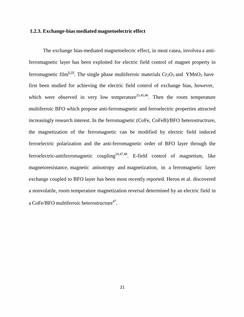
electric field modification of effective magnetic field was 202 Oe(Fig 1.3(b)).
22
Fig 1.3 (a) FMR fields of NiFe/Cu/PMN-PT(011) and (b) NiFe/PMN-PT(011) upon applying different
electric fields with the bias magnetic field applied along the in-plane [0–11] direction. Insets show
schematic of NiFe/PMN-PT heterostructure (up) with strain and surface charge at the interface
and NiFe/Cu/PMN-PT heterostructure with only strain at the interface(down).113
23
Chapter 2: Fabrication and Characterization
In this chapter, the fabrication and characterization of the multiferroic
heterostructures are presented. The physical vapor deposition which is the main thin film
deposition method in this work is introduced in detail. The characterization methods is
categorized in ferroelectric polarization measurement, static magnetic property
measurement, high frequency ferromagnetic resonance measurement and magnetoelctric
coefficient measurement.
2.1. Metallic magnetic thin film fabrication: physical vapor deposition system (PVD)
PVD is a variety of vacuum deposition methods used to deposit thin films by the
condensation of a vaporized form of the desired film material onto various work piece
surfaces. The coating method involves purely physical processes such as high
temperature vacuum evaporation with subsequent condensation, or plasma sputter
bombardment rather than involving a chemical reaction at the surface to be coated as in
chemical vapor deposition (CVD). PVD coatings are sometimes harder and more
corrosion resistant than coatings applied by the electroplating process. Most coatings
have high temperature and good impact strength, excellent abrasion resistance and are so
durable that protective topcoats are almost never necessary.
24
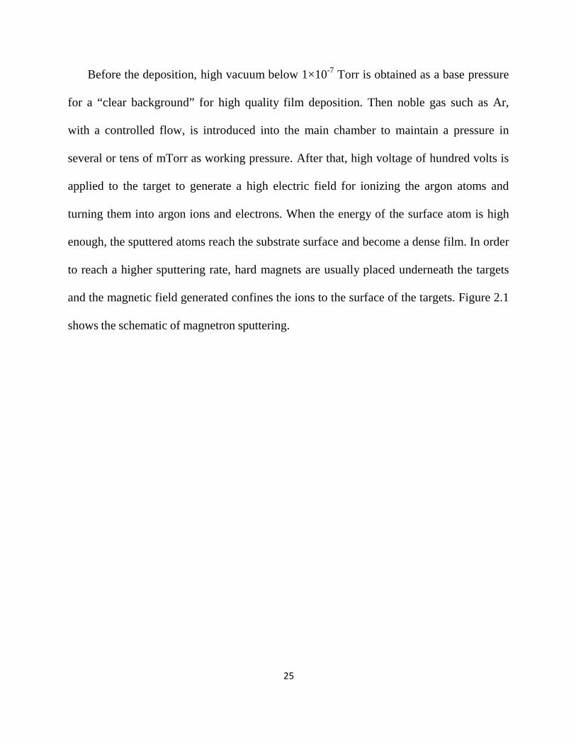
Before the deposition, high vacuum below 1×10⁻⁷ Torr is obtained as a base pressure
for a “clear background” for high quality film deposition. Then noble gas such as Ar,
with a controlled flow, is introduced into the main chamber to maintain a pressure in
several or tens of mTorr as working pressure. After that, high voltage of hundred volts is
applied to the target to generate a high electric field for ionizing the argon atoms and
turning them into argon ions and electrons. When the energy of the surface atom is high
enough, the sputtered atoms reach the substrate surface and become a dense film. In order
to reach a higher sputtering rate, hard magnets are usually placed underneath the targets
and the magnetic field generated confines the ions to the surface of the targets. Figure 2.1
shows the schematic of magnetron sputtering.
25
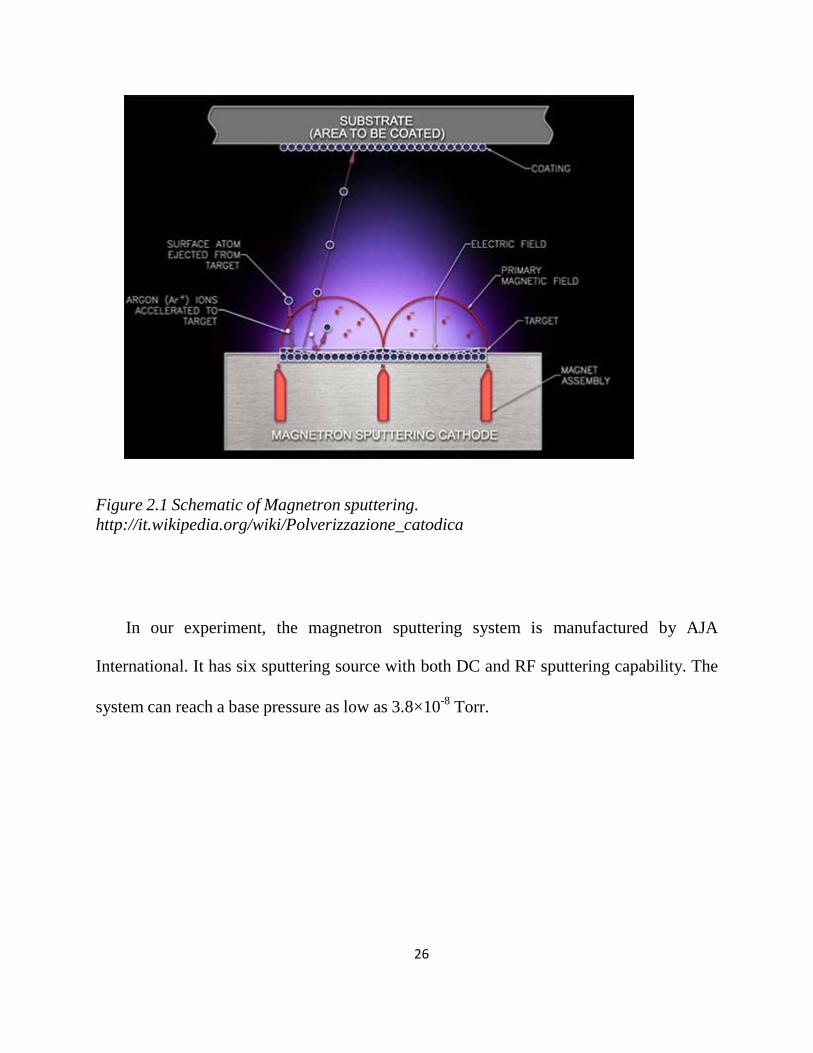
Figure 2.1 Schematic of Magnetron sputtering. http://it.wikipedia.org/wiki/Polverizzazione_catodica
In our experiment, the magnetron sputtering system is manufactured by AJA
International. It has six sputtering source with both DC and RF sputtering capability. The
system can reach a base pressure as low as 3.8×10⁻⁸ Torr.
26
2.2. Ferroelectric characterization
In order to measure the electric polarization of ferroelectric substrates, the Radient
Precision LC ferroelectric test system is used. This is very important in our experiments
since electric coercive field, remnant polarization and etc. of ferroelectric materials are
critical parameters for reaching non-volatile switching of magnetism. Considering the
thickness (~500um) and electric field (~10 kV/cm) needed in the experiments, up to 600
V is required. For that requirement, a high voltage interface and a high voltage amplifier
with a gain of 1000 are also connected to the ferroelectric test system to generate large
electric fields. Figure 2.2 shows the Radient Precision LC ferroelectric test system.
27
Figure 2.2 Radient Precision LC ferroelectric test system.
2.3. Static magnetic property characterization: vibration sample magnetometer (VSM)
In this experiments, the vibrating sample magnetometer (VSM) is used to measure the
DC/low frequency magnetic properties of magnetic materials. A VSM system consists of
a vibration stage, a pick-up coils and electromagnets. The sample is loaded on the
vibration stage that vibrates at certain frequency, and then the pick-up coils are used to
detect the change of the magnetic flux. Due to the Faraday’s law, the magnetization in
different bias magnetic field generated by the electromagnets can be obtained by the
28
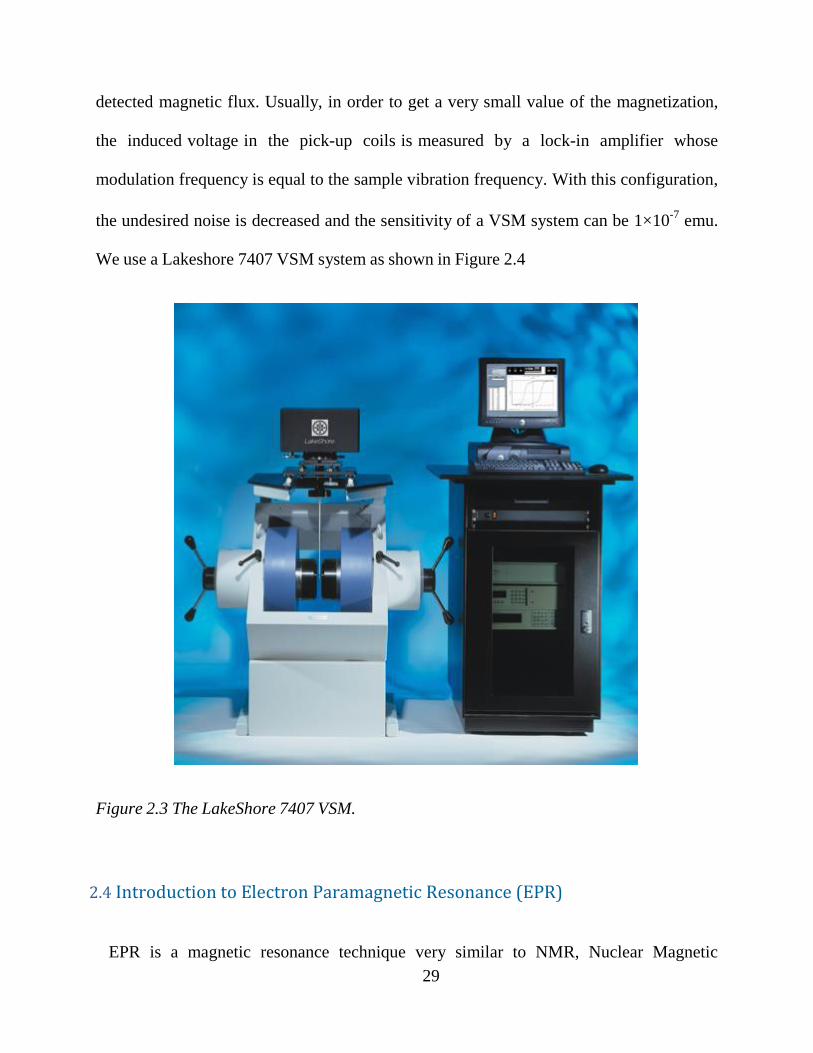
detected magnetic flux. Usually, in order to get a very small value of the magnetization,
the induced voltage in the pick-up coils is measured by a lock-in amplifier whose
modulation frequency is equal to the sample vibration frequency. With this configuration,
the undesired noise is decreased and the sensitivity of a VSM system can be 1×10⁻⁷ emu.
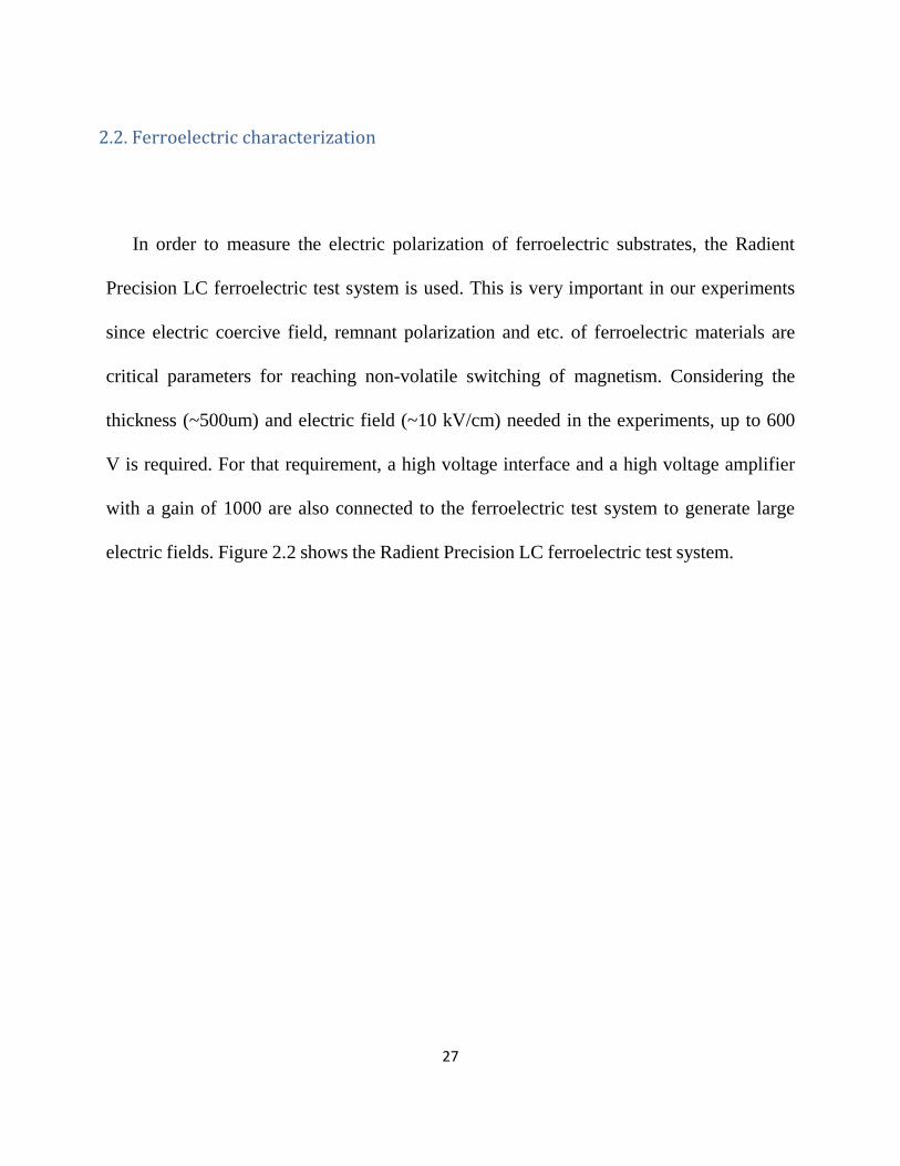
We use a Lakeshore 7407 VSM system as shown in Figure 2.4
Figure 2.3 The LakeShore 7407 VSM.
2.4 Introduction to Electron Paramagnetic Resonance (EPR)
EPR is a magnetic resonance technique very similar to NMR, Nuclear Magnetic 29
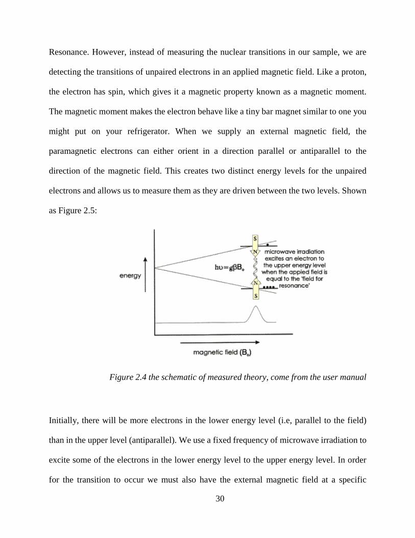
Resonance. However, instead of measuring the nuclear transitions in our sample, we are
detecting the transitions of unpaired electrons in an applied magnetic field. Like a proton,
the electron has spin, which gives it a magnetic property known as a magnetic moment.
The magnetic moment makes the electron behave like a tiny bar magnet similar to one you
might put on your refrigerator. When we supply an external magnetic field, the
paramagnetic electrons can either orient in a direction parallel or antiparallel to the
direction of the magnetic field. This creates two distinct energy levels for the unpaired
electrons and allows us to measure them as they are driven between the two levels. Shown
as Figure 2.5:
Figure 2.4 the schematic of measured theory, come from the user manual
Initially, there will be more electrons in the lower energy level (i.e, parallel to the field)
than in the upper level (antiparallel). We use a fixed frequency of microwave irradiation to
excite some of the electrons in the lower energy level to the upper energy level. In order
for the transition to occur we must also have the external magnetic field at a specific
30
strength, such that the energy level separation between the lower and upper states is exactly
matched by our microwave frequency. In order to achieve this condition, we sweep the
external magnet's field while exposing the sample to a fixed frequency of microwave
irradiation. The condition where the magnetic field and the microwave frequency are "just
right" to produce an EPR resonance (or absorption) is known as the resonance condition
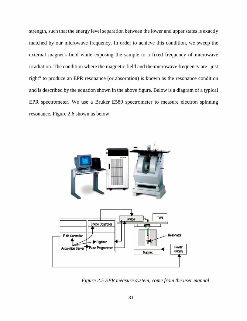
and is described by the equation shown in the above figure. Below is a diagram of a typical
EPR spectrometer. We use a Bruker E580 spectrometer to measure electron spinning
resonance, Figure 2.6 shown as below,
Figure 2.5 EPR measure system, come from the user manual
31
Chapter 3. Voltage Control of Magnetism in FeGaB/ PIN-PMN-PT Heterostructures 3.1. Introduction
Multiferroic composites with combined ferromagnetic (FM) and ferroelectric (FE)
phases have attracted extensive attention due to their strong magnetoelectric (ME) coupling
at room temperature.3-8 Specifically in magnetic-piezoelectric heterostructures, an electric
field E applied to the piezoelectric layer produces a mechanical deformation that couples
to the magnetic layer, and thus induces a change in the magnetization, ferromagnetic
resonance field, ferromagnetic resonance frequency, or magnetic permeability.49-51 This
converse ME coupling leads to effective E-field control of magnetism such as E-field
tunable magnetic hysteresis loops, E-field tunable permeability, and E-field control of
ferromagnetic resonance (FMR), which exhibits promising applications in tunable radio
frequency (RF) microwave devices, multiple-state memories, spintronics, and magnetic
field sensors.49-51
Recently, giant E-field-induced FMR tunability has been demonstrated in multiferroic
composites using relaxor-based lead magnesium niobate–lead titanate (PMN-PT) and lead
zinc niobate–lead titanate (PZN-PT) single crystals with high piezoelectric coefficients.8-
10 Unlike conventional devices where magnetic fields are used for FMR tuning, the E-field
tuning process is fast, and power efficient as the biasing voltages applied on single crystals
involve minimal currents. Therefore, these magnetic-piezoelectric heterostructures show
great potential for the next-generation of compact, lightweight, and energy-efficient RF 32
microwave devices. However, the E-field tunable range has been limited by the electric
coercive field. For example, the largest tunability is typically achieved between -2 and 6
kV/cm for multiferroic composites based on PMN-PT and PZN-PT due to low coercive
field (~2 kV/cm).9-10 Under high electric field, the devices are susceptible to failure from
corona breakdown induced by bias fields. Moreover, the low temperature stability of
rhombohedral phase with TRT ~75–95 °C would lead to undesirable changes in
performance with temperature.
To expand the operating conditions and enhance stability of piezo-crystal-based
multiferroic composites, in this work, ternary single crystals lead indium niobate–lead
magnesium niobate–lead titanate (PIN-PMN-PT) are used to fabricate novel FeGaB/PIN-
PMN-PT heterostructures. Large E-field tuning of FMR is demonstrated in these
heterostructures, comparable to that of the composites based on PMN-PT and PZN-PT.
With higher coercive field and TRT >120 °C for PIN-PMN-PT,11-15 multiferroic
FeGaB/PIN-PMN-PT heterostructures can be potential candidates for high-power tunable
RF/microwave devices with wider temperature operational range.
3.2 Experiment
Multiferroic composites FeGaB/PIN-PMN-PT were prepared by co-sputtering of
Fe80Ga20 and B targets onto (011)-poled PIN-PMN-PT substrates with a base pressure
below 1 × 10⁻⁷ Torr at room temperature. The thickness of FeGaB film is determined to
be 50 nm by fitting X-ray reflectivity (XRR). 5 nm Cu was then sputtered on top of FeGaB 33
as a capping layer. The ferroelectric property of PIN-PMN-PT was measured by the
Radiant Ferroelectric characterization system. The strain vs E curve was measured using a
photonic sensor by sweeping the sinusoidal electric field. The ferromagnetic resonance
(FMR) spectra were measured using an X-band electron spin resonance (ESR)
spectrometer in field sweeping mode with a microwave frequency of 9.5 GHz and a power
of -20 dBm. In the FMR field angular dependence measurements, the samples were taped
on the sample holder with a precise angle rotator. The magnetic hysteresis loops were
measured using a vibrating sample magnetometer (VSM, Lakeshore 7400). During the
VSM and FMR measurements, DC electric fields were applied through the thickness
direction of PIN-PMN-PT, which was coated with Au on the back as an electrode.
3.3 Results and discussion
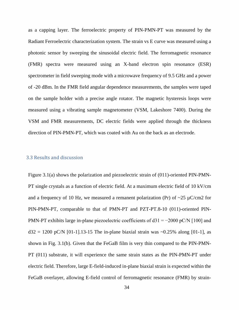
Figure 3.1(a) shows the polarization and piezoelectric strain of (011)-oriented PIN-PMN-
PT single crystals as a function of electric field. At a maximum electric field of 10 kV/cm
and a frequency of 10 Hz, we measured a remanent polarization (Pr) of ~25 µC/cm2 for
PIN-PMN-PT, comparable to that of PMN-PT and PZT-PT.8-10 (011)-oriented PIN-
PMN-PT exhibits large in-plane piezoelectric coefficients of d31 = −2000 pC/N [100] and
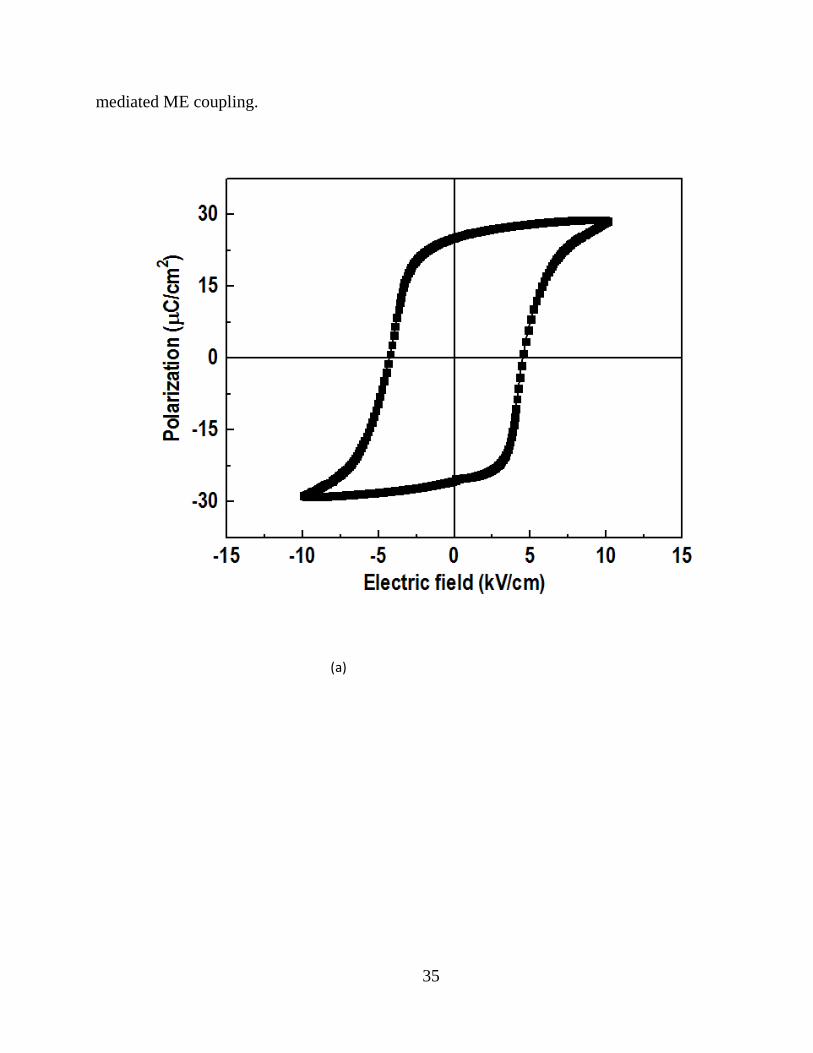
d32 = 1200 pC/N [01-1].13-15 The in-plane biaxial strain was ~0.25% along [01-1], as
shown in Fig. 3.1(b). Given that the FeGaB film is very thin compared to the PIN-PMN-
PT (011) substrate, it will experience the same strain states as the PIN-PMN-PT under
electric field. Therefore, large E-field-induced in-plane biaxial strain is expected within the
FeGaB overlayer, allowing E-field control of ferromagnetic resonance (FMR) by strain-
34
mediated ME coupling.
(a)
35
(b)
Fig.3.1 Polarization and piezoelectric strain of (011) oriented PIN-PMN-PT as a function
of electric field, where the electric coercive field was found at ±6.7 kV/cm
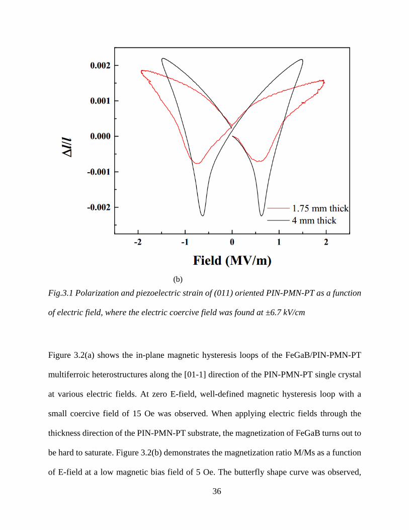
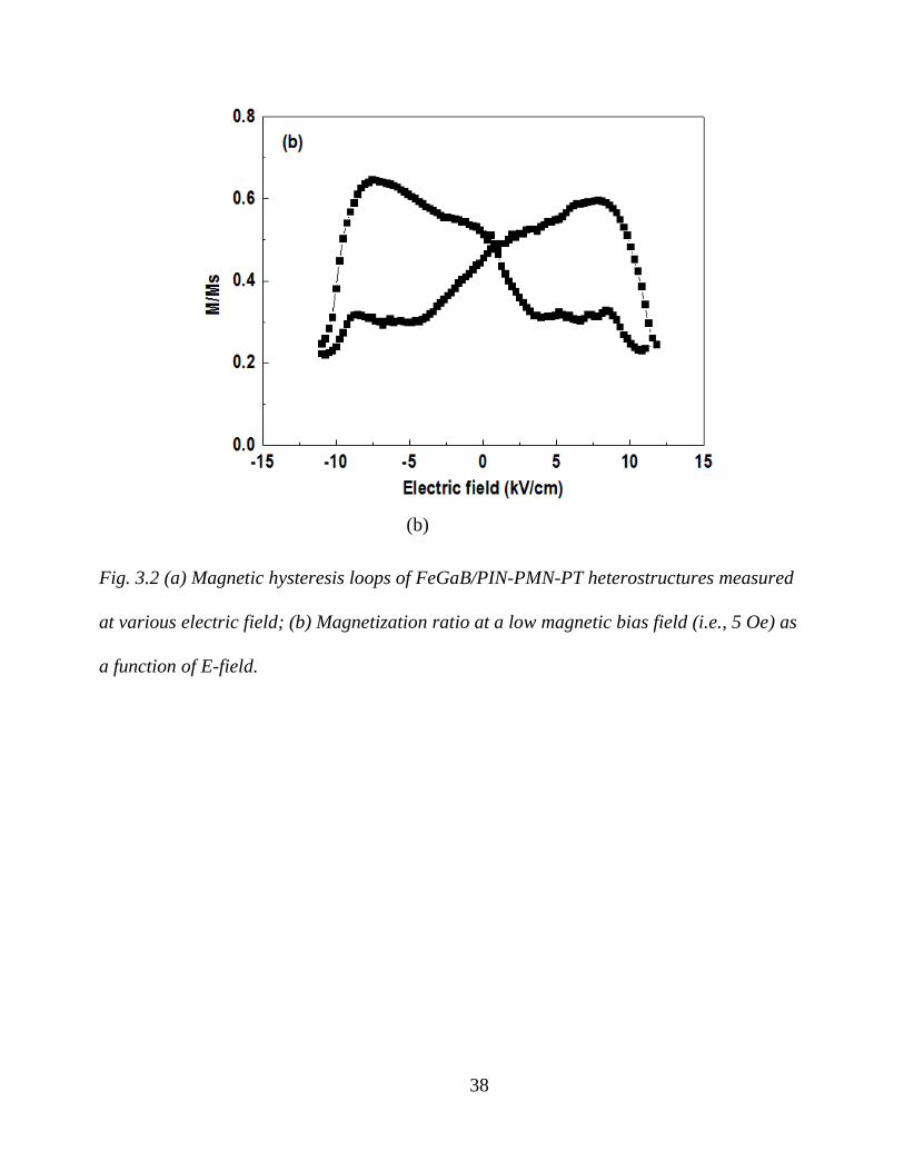
Figure 3.2(a) shows the in-plane magnetic hysteresis loops of the FeGaB/PIN-PMN-PT
multiferroic heterostructures along the [01-1] direction of the PIN-PMN-PT single crystal
at various electric fields. At zero E-field, well-defined magnetic hysteresis loop with a
small coercive field of 15 Oe was observed. When applying electric fields through the
thickness direction of the PIN-PMN-PT substrate, the magnetization of FeGaB turns out to
be hard to saturate. Figure 3.2(b) demonstrates the magnetization ratio M/Ms as a function
of E-field at a low magnetic bias field of 5 Oe. The butterfly shape curve was observed,
36
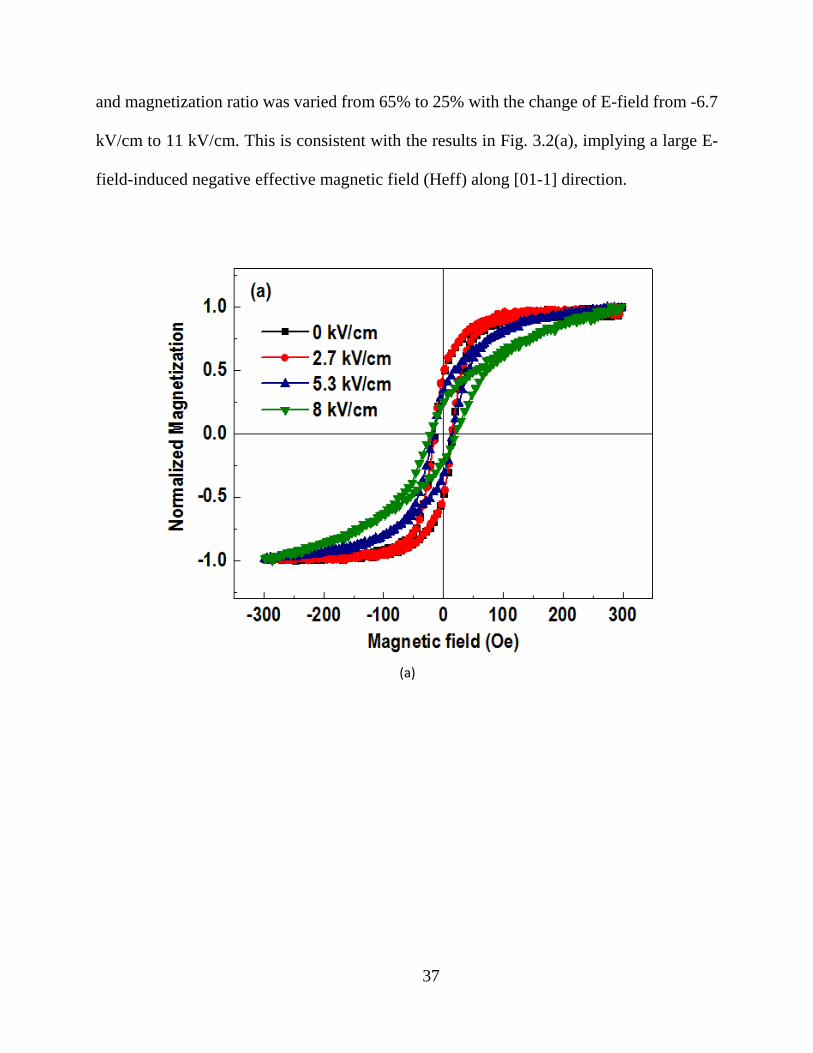
and magnetization ratio was varied from 65% to 25% with the change of E-field from -6.7
kV/cm to 11 kV/cm. This is consistent with the results in Fig. 3.2(a), implying a large E-
field-induced negative effective magnetic field (Heff) along [01-1] direction.
(a)
37
(b)
Fig. 3.2 (a) Magnetic hysteresis loops of FeGaB/PIN-PMN-PT heterostructures measured
at various electric field; (b) Magnetization ratio at a low magnetic bias field (i.e., 5 Oe) as
a function of E-field.
38
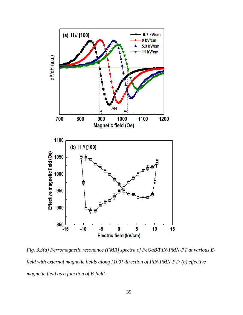
Fig. 3.3(a) Ferromagnetic resonance (FMR) spectra of FeGaB/PIN-PMN-PT at various E-
field with external magnetic fields along [100] direction of PIN-PMN-PT; (b) effective
magnetic field as a function of E-field.
39
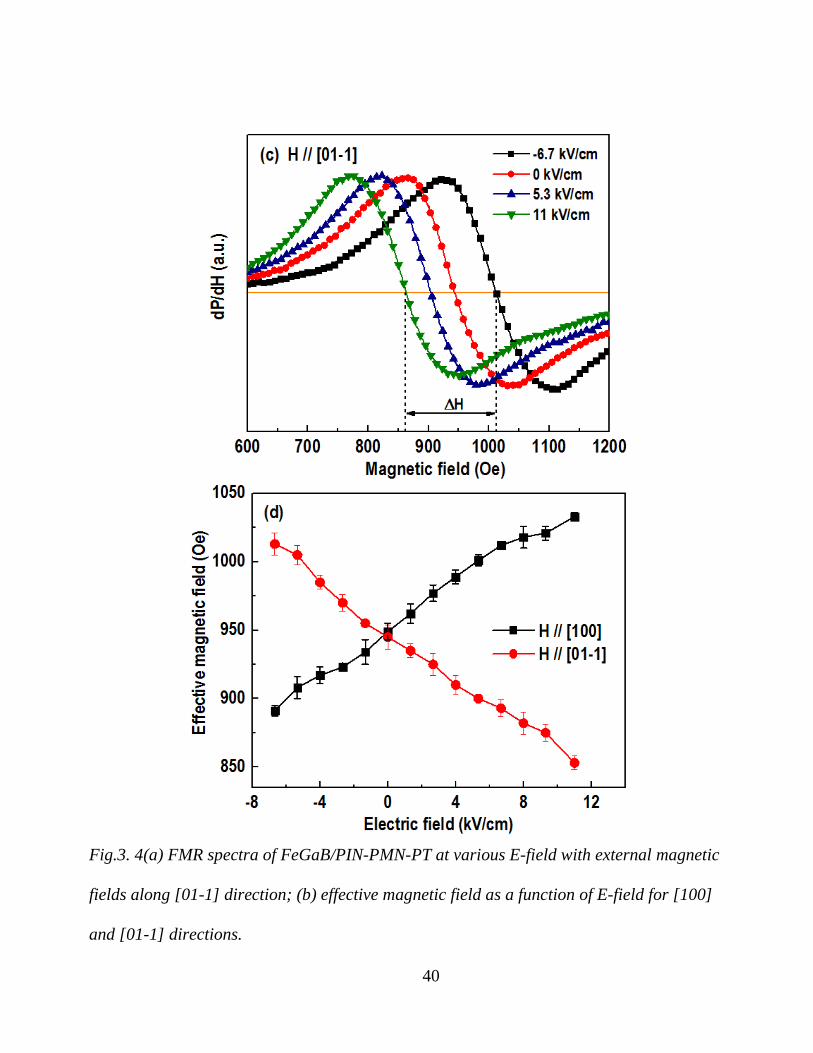
Fig.3. 4(a) FMR spectra of FeGaB/PIN-PMN-PT at various E-field with external magnetic
fields along [01-1] direction; (b) effective magnetic field as a function of E-field for [100]
and [01-1] directions.
40
The field-sweep ferromagnetic resonance (FMR) spectra of the FeGaB/PIN-PMN-PT
multiferroic composites under different electric fields are shown in Fig.3. 3(a). A microwave
cavity operating at TE102 mode and X-band (9.5 GHz) was used to perform FMR
measurements of the ferromagnetic/piezoelectric multiferroic. The external bias magnetic
field was applied in the FeGaB film plane along the PIN-PMN-PT [100] (Fig. 3.3(a)) or
[01–1] directions (Fig. 3.4(a)), with the microwave RF field in-plane and perpendicular to
the DC bias field. Clearly, strong microwave ME interaction was observed in FeGaB/PIN-
PMN-PT, which resulted in a high tunable FMR field range from 891 Oe to 1033 Oe when
the electric fields across the PIN-PMN-PT thickness were changed from -6.7 kVcm to 11
kVcm. In FeGaB/PIN-PMN-PT heterostructures, the screening charges induced by
ferroelectric polarization may exist at the interface of FeGaB and PIN-PMN-PT. However,
for FeGaB with a thickness of 50 nm, the interfacial charge mediated ME coupling is
negligible. Thus pure strain mediated magnetoelectric coupling was controlled by the
electric field applied on the PIN-PMN-PT due to the piezoelectric effect. As expected, a
butterfly-like curve of the FMR effective magnetic field (Heff) as a function of electric field
was observed, as shown in Fig. 3.3(b), having a maximum Heff tunability of 142 Oe. The
effective magnetic field as a function of E-field shares a similar shape with that of the
piezoelectric strain of PIN-PMN-PT which has a sudden jump at the electric coercive field
of > 6.7 kV/cm. The links between the Heff -E and σ-E curves demonstrate the control of the
effective magnetic field by E-field via strain mediated mechanism.
According to Kittel equation, the in-plane FMR frequency can be expressed as: 41
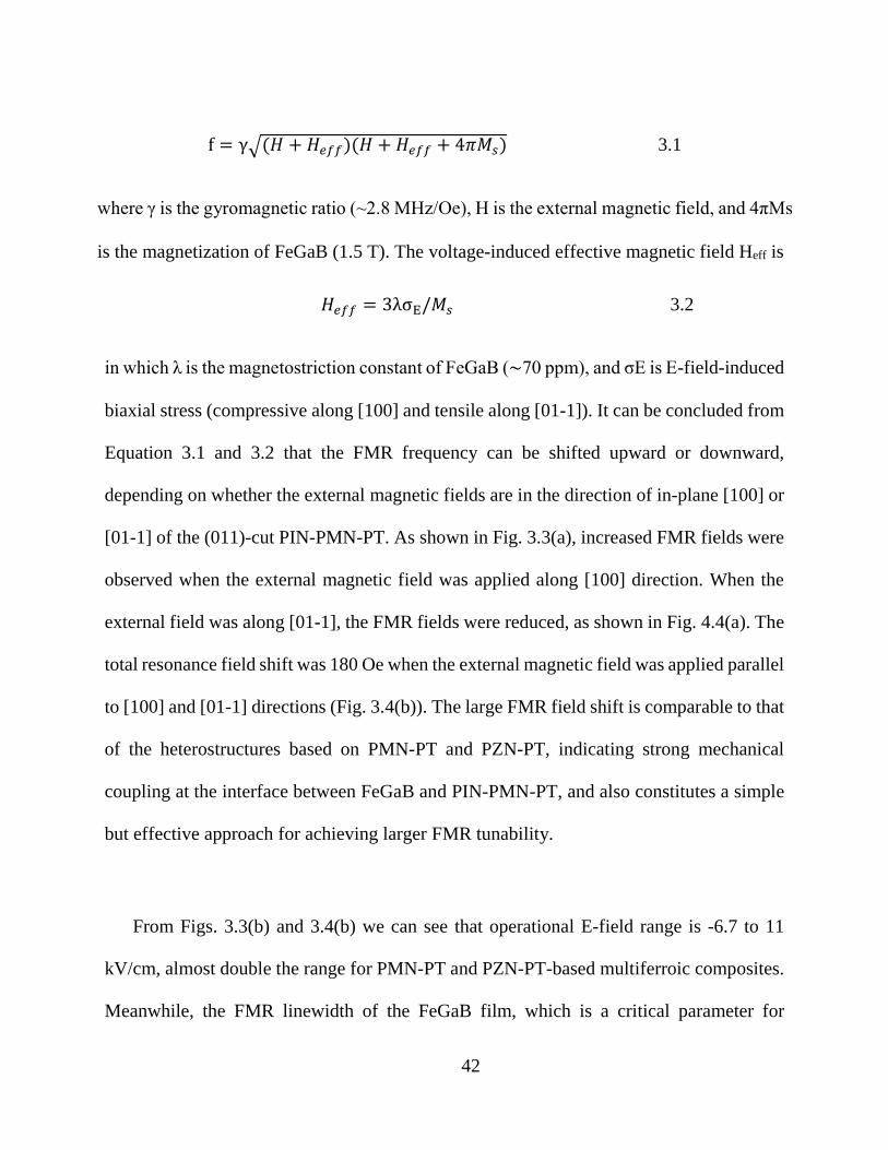
f = γ�(𝐻𝐻 + 𝐻𝐻𝑒𝑒𝑒𝑒𝑒𝑒)(𝐻𝐻 + 𝐻𝐻𝑒𝑒𝑒𝑒𝑒𝑒 + 4𝜋𝜋𝑀𝑀𝑠𝑠) 3.1
where γ is the gyromagnetic ratio (~2.8 MHz/Oe), H is the external magnetic field, and 4πMs
is the magnetization of FeGaB (1.5 T). The voltage-induced effective magnetic field Heff is
𝐻𝐻𝑒𝑒𝑒𝑒𝑒𝑒 = 3λσE/𝑀𝑀𝑠𝑠 3.2
in which λ is the magnetostriction constant of FeGaB (∼70 ppm), and σE is E-field-induced
biaxial stress (compressive along [100] and tensile along [01-1]). It can be concluded from
Equation 3.1 and 3.2 that the FMR frequency can be shifted upward or downward,
depending on whether the external magnetic fields are in the direction of in-plane [100] or
[01-1] of the (011)-cut PIN-PMN-PT. As shown in Fig. 3.3(a), increased FMR fields were
observed when the external magnetic field was applied along [100] direction. When the
external field was along [01-1], the FMR fields were reduced, as shown in Fig. 4.4(a). The
total resonance field shift was 180 Oe when the external magnetic field was applied parallel
to [100] and [01-1] directions (Fig. 3.4(b)). The large FMR field shift is comparable to that
of the heterostructures based on PMN-PT and PZN-PT, indicating strong mechanical
coupling at the interface between FeGaB and PIN-PMN-PT, and also constitutes a simple
but effective approach for achieving larger FMR tunability.
From Figs. 3.3(b) and 3.4(b) we can see that operational E-field range is -6.7 to 11
kV/cm, almost double the range for PMN-PT and PZN-PT-based multiferroic composites.
Meanwhile, the FMR linewidth of the FeGaB film, which is a critical parameter for
42
microwave magnetic materials, stays under 120±20Oe at different electric fields. The ratio
between the total tunable magnetic field and the FMR linewidth is as high as 150%,
indicating an excellent figure of merit for tunable microwave devices.
3.4. Conclusion In summary, we have demonstrated large FMR tunability through E-field induced, strain
mediated ME coupling in FeGaB/PIN-PMN-PT multiferroic composites. A large effective
magnetic anisotropy field change of 180 Oe was obtained, comparable to that of the
composites based on PMN-PT and PZN-PT. operational E-field range is -6.7 to 11 kV/cm,
almost double the range for PMN-PT and PZN-PT-based multiferroic composites. With a
high phase transition temperature TRT >120 °C for PIN-PMN-PT, FeGaB/PIN-PMN-PT
heterostructures have great potential for high-power tunable RF/microwave device
application with wider temperature operational range.
43
Chapter 4. E-tuning of FMR in ultrathin NiFe/PLZT heterostructures 4.1 Introduction
Strong magnetoelectric coupling has been recently dem- onstrated in different
magnetic/ferroelectric and magnetic/di- electric thin film heterostructures, which enables
power efficient voltage control of magnetism and magnetic manipulation of electric
polarization, and has gained much interest in the recent decade. Magnetoelectric spintronics
and tunable RF/microwave applications have been demonstrated 51-56, including voltage
tunable resonators,57 magnetic field sensors,58 tunable inductors,9 and tunable fil- ters.60’61
Strain-mediated magnetoelectric coupling has been investigated in both ferromagnetic (FM)
thin film/ferroelec- tric (FE) slab heterostructures61–65 and in FM/FE66,67 thin film
heterostructures. Thin film heterostructures have the advantage of requiring a relatively
lower tuning voltages (<rv30 V) compared to magnetoelectric heterostructures with thick
FE slabs which need high tuning voltages of up to 400–600 V. However, the strain mediated
magnetoelectric coupling was significantly reduced in thin film hetero- structures by
substrate clamping effect.66,67
Other magnetoelectric coupling mechanisms in thin film magnetoelectric
heterostructures were reported, in which ME coupling was not limited by substrate
clamping effect, such as interfacial spin-polarized charge-mediated magnetoelectric
coupling in magnetic/ferroelectric68-76 or magnetic/dielectric77-81 thin film heterostructures,
interfacial exchange coupling in magnetic/multiferroic thin film heterostructures82-87
44
Charge-mediated magnetoelectric coupling leads to a voltage controllable interface
magnetic anisotropy at the magnetic/dielectric or magnetic/ferroelectric interface, which is
directly related to the spin polarized charge at the interface. Surface charge induced
magnetic surface anisotropy change in Fe/BaTiO3 heterostructure was estimated
through density-functional calculations; giant magnetoelectric coupling behavior was
experimentally demonstrated in Fe/MgO heterostructures. Other magnetic/ferroelectric
multiferroics heterostructure, such as, La0.8Sr0.2MnO3/PbZr 0.2 Ti0.8 O3, was studied and
large ME coupling coefficient of 0.8 x 10⁻³ Oe cm V-1 was obtained. Spin-polarized
charge mediate ME coupling was also predicted in magnetic/dielectric heterostructure like,
SrRuO3/SrTiO3, theoretically and was realized experimentally in Fe/MgO and CoFe/MgO
heterostructures. Combined voltage controlled charge-mediated magnetoelectric coupling
and strain-mediated magnetoelectric coupling were also reported in Ni/Pb(Zr0.52Ti0.48)O3
(PZT)25 and Ni/BaTiO3 (BTO)26 heterostructures. Further, pure interfacial charge effect
was systematically investigated in very thin FM film (<1 nm) on dielectric layer (MgO).77–
81 Large voltage tunable effective magnetic anisotropy change up to 20 kJ/m3 was
achieved in Fe/MgO thin film heterostructures.
In the previous research, people found that the charge mediated ME coupling strength
is highly dependent on magnetic film thickness.27,28 For instance, ME coupling strength of
Fe/MgO heterostructure measured by Kerr hysteresis loop was significantly dependent on
Fe film thickness, where the maximum magnetic surface anisotropy change was obtained
at spin reorientation Fe thickness. In Co20Fe80/MgO heterostructure, magnetic surface
45
anisotropy change decreased rapidly as Co20Fe80 film thicknesses were larger than 0.5 nm.
Nevertheless, the mechanism causing charge mediated ME coupling strength dependence
on magnetic film thickness is still not clear. To obtain more understanding of the charge
mediated ME coupling tunability, Zhou et al has reported the tunability of charge mediated
ME coupling on Ni0.81 Fe0.19(NiFe)/STO dielectric thin film. The FMR field shift is 65Oe.
However, there is not polarization-electric field loop for STO thin film, that means there is
no residual electric charge at zero voltage.
To optimize the charge mediated ME coupling tunability in real applications and study
the Voltage Impulse Induced Bistable Magnetization Switching, we studied the voltage
dependent ferromagnetic resonance (FMR) in Ni0.81Fe0.19 (NiFe)/ Pb(Zr0.52Ti0.48)O3
(PZT)) magnetic/dielectric thin film heterostructures to quantitatively determine the
thickness dependence of charge mediated magnetoelectric coupling. Voltage induced
FMR field change was carried out through charge effect induced magnetic surface
anisotropy change. Large voltage induced FMR field shift of 72 Oe and magnetic surface
anisotropy change of 5.6 kJ/m3 were obtained in NiFe/PLZT heterostructures. The voltage
induced magnetic surface anisotropy showed a strong dependence on the thickness of the
magnetic thin films, which was discussed based on the thin film growth model at the low
thickness side and on the charge screening effect at large thickness side. This precise
quantification and further understanding of the magnetoelectric coupling in mag-
netic/dielectric thin film heterostructures pave the way toward their applications in compact,
fast, energy efficient in voltage tunable RF/microwave devices and spintronics.
46
4.2 Experiment
Multilayer dielectric/magnetic thin film heterostructures Ti (20 nm)/Pt (20 nm)/
Pb(Zr0.52Ti0.48)O3 (PZT, 350 nm)/Ni0.81Fe0.19 (01nm–2.8 nm)/Cu (3 nm) with different
NiFe layer thicknesses were deposited by magnetron sputtering system on Si(111) substrate
(0.5 mm). PLZT precursor solutions (0.5 M) with various Zr/Ti ratios (Zr/Ti=52/48) were
prepared by a modified 2-methoxyethanol synthesis route. In the solutions, 8 mol%
lanthanum was added to enhance the relaxor behavior and insulating property. The starting
chemicals were lead acetate trihydrate, lanthanum nitrate hexahydrate, zirconium propoxide,
and titanium isopropoxide. Excess lead (20 mol%) was used to compensate for the lead loss
during the high temperature crystallization. Detailed solution synthesis conditions can be
found in our prior report. The PLZT films were grown by spin coating the solution on PtSi
substrates at 3000 rpm for 30 s. Each layer was pyrolyzed at 450 oC for 10 min before being
annealed at 650 oC for 5 min. An additional annealing at 650 oC for 5 min was applied after
every three layers of coating. A final crystallization anneal was performed at 650 oC for 15
min. The thickness of the PLZT films with six layers of coating was ≈690 nm, resulting in a
per-coating thickness of ≈115 nm. Platinum top electrodes with a diameter of 250 μm and a
thickness of 100 nm were deposited on the prepared samples through a shadow mask by
electron-beam evaporation. The NiFe Films of a 200um x 200um were sputtered onto the
PZT films at room temperature. 3nm Cu was deposited on each NiFe layer as the capping
layer. X-ray diffraction (XRD) system with Cu Ka radiation was used to measure the chemical
47
lattice structure of the NiFe/PLZT multiferroic structure. Atomic Force Microscope (AFM)
was used to measured PLZT surface. The magneticproperties were characterized using
Electron Paramagnetic Resonance (EPR) system at X-band (9.56GHz) and magneto-optocal
Kerr effect (MOKE) magnetometer, respectively. Polarization vs applied voltage (P-V) loop
of PLZT was taken by the radiance ferroelectric system. There was a small DC voltage was
perpendicularly applied across the PLZT film between the upper NiFe film and bottom Pt
electrodes. Fig 4.2(a) shows the measurement apparatus. All these measurements were
measured at room temperature.
4.3 Results and Discussion X-ray diffraction (XRD) patterns of the PLZT films are shown in Figure 4.1(a). All the
diffraction patterns show only well-crystallized polycrystalline perovskite phases, together
with Si substrate, and can be well indexed by a pseudocubic structure. No other phases were
detected, suggesting that neither pyrochlore phases nor interfacial reactions affected the
structure. Figure 3.1(a) shows the polarization and piezoelectric strain of PLZT thin film as
a function of electric field. At a maximum electric field of 300 kV/cm and a frequency of 10
Hz, we measured a remanent polarization (Pr) of ~25 µC/cm2 for PLZT. The surface of
48
20 30 40 50 60
211200111110
Inte
nsity
2θ
substrate PLZT
100
(a)
-300 -150 0 150 300-50
-25
0
25
50
Pol
ariz
atio
n(µC
/cm
2 )
Elecytric Feild (kV/cm)
(b)
49
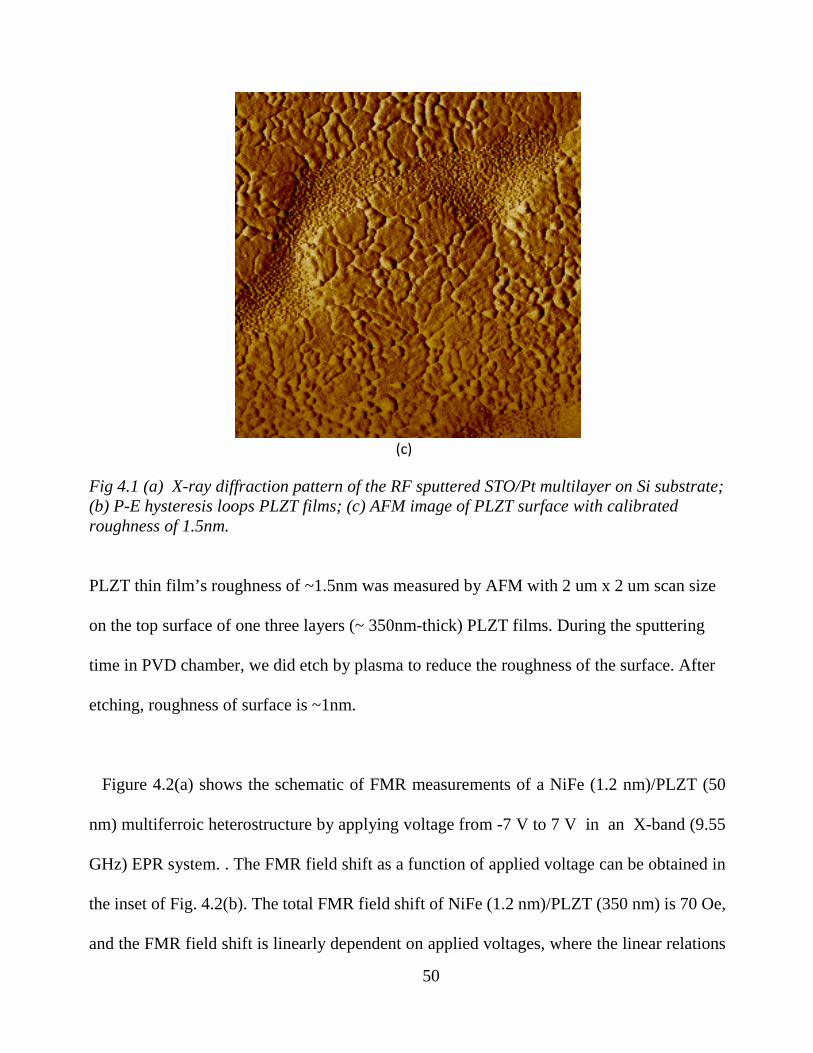
(c) Fig 4.1 (a) X-ray diffraction pattern of the RF sputtered STO/Pt multilayer on Si substrate; (b) P-E hysteresis loops PLZT films; (c) AFM image of PLZT surface with calibrated roughness of 1.5nm. PLZT thin film’s roughness of ~1.5nm was measured by AFM with 2 um x 2 um scan size
on the top surface of one three layers (~ 350nm-thick) PLZT films. During the sputtering
time in PVD chamber, we did etch by plasma to reduce the roughness of the surface. After
etching, roughness of surface is ~1nm.
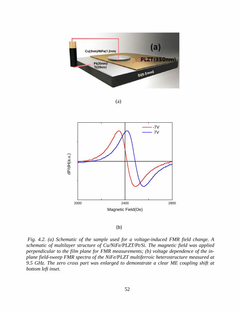
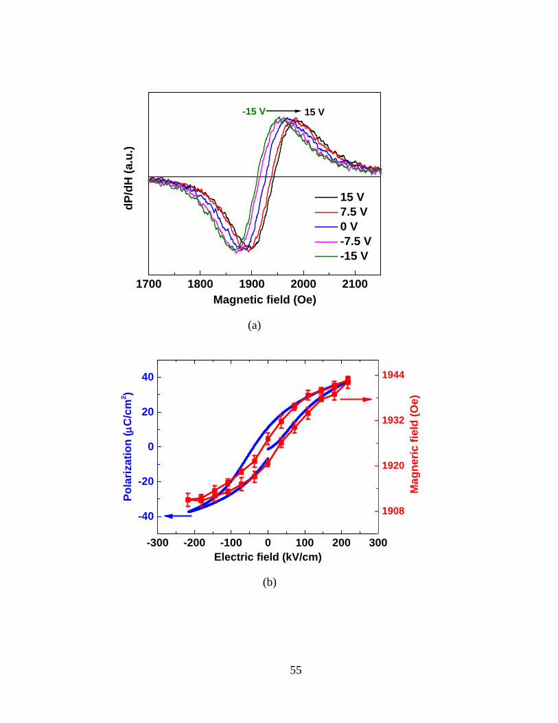
Figure 4.2(a) shows the schematic of FMR measurements of a NiFe (1.2 nm)/PLZT (50
nm) multiferroic heterostructure by applying voltage from -7 V to 7 V in an X-band (9.55
GHz) EPR system. . The FMR field shift as a function of applied voltage can be obtained in
the inset of Fig. 4.2(b). The total FMR field shift of NiFe (1.2 nm)/PLZT (350 nm) is 70 Oe,
and the FMR field shift is linearly dependent on applied voltages, where the linear relations
50
between interfacial charge mediated magnetoelectric coupling strength and applied voltage
are also observed in previously reports. From Zhou et al reports that an angle-independent
isotropic FMR field shift around 60 Oe was observed, consistent with a surface charge
induced out-of-plane magnetic surface anisotropy change. The total perpendicular magnetic
energy of NiFe thin film can be expressed as 27-31:
Eperpd= - ½ µ0Ms2 d + Ks,NiFe/Cu + Ks,NiFe/PLZT + ∆Ks(V) 4.1
Where Eperp, Ms, µ0, and d are perpendicular anisotropy energy, saturation magnetization,
permeability of free space, and magnetic film thickness, respectively. Surface anisotropy
between NiFe/Cu and NiFe/PLZT interface are Ks,NiFe/Cu and Ks,NiFe/PLZT, respectively, and
∆Ks(V) is the charge induced magnetic surface anisotropy change. Figure 4.2 (a) shows the
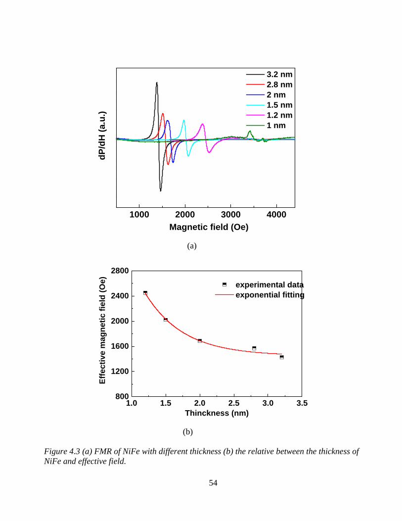
FMR of NiFe with different thickness. That was demonstrated the perpendicular magnetic
energy and corresponding FMR field increases monotonically as the NiFe thickness d
decreases. The total energy of NiFe film can be expressed as
Etotal = -H*M – 2πMs2 + (Ks,NiFe/Cu + Ks,NiFe/PLZT + ∆Ks(V))/d. 4.2
51
(a)
2000 2400 2800
-7V 7V
dP/d
H(a
.u.)
Magnetic Field(Oe)
(b)
Fig. 4.2. (a) Schematic of the sample used for a voltage-induced FMR field change. A schematic of multilayer structure of Cu/NiFe/PLZT/Pt/Si. The magnetic field was applied perpendicular to the film plane for FMR measurements; (b) voltage dependence of the in-plane field-sweep FMR spectra of the NiFe/PLZT multiferroic heterostructure measured at 9.5 GHz. The zero cross part was enlarged to demonstrate a clear ME coupling shift at bottom left inset.
52
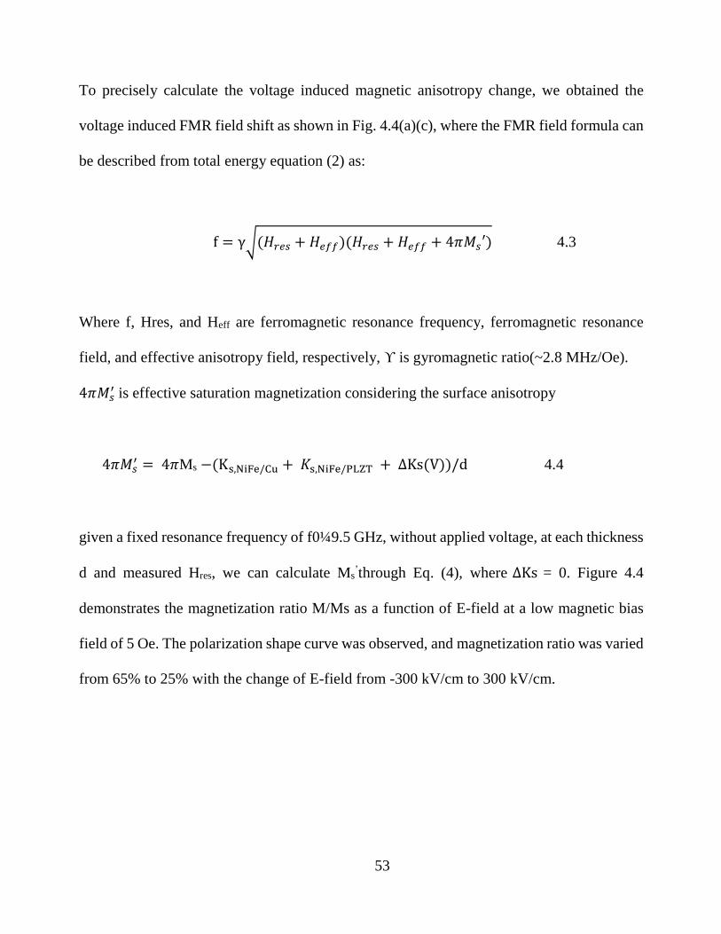
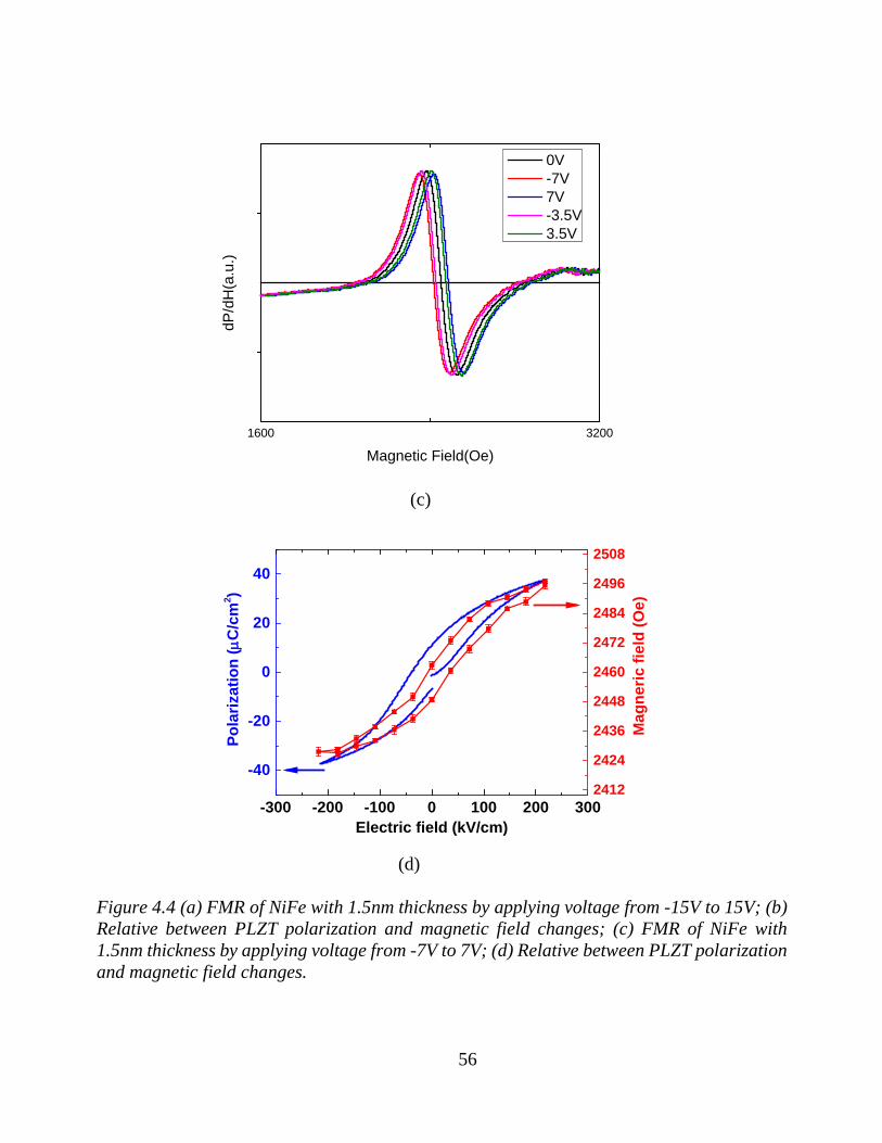
To precisely calculate the voltage induced magnetic anisotropy change, we obtained the
voltage induced FMR field shift as shown in Fig. 4.4(a)(c), where the FMR field formula can
be described from total energy equation (2) as:
f = γ�(𝐻𝐻𝑟𝑟𝑒𝑒𝑠𝑠 + 𝐻𝐻𝑒𝑒𝑒𝑒𝑒𝑒)(𝐻𝐻𝑟𝑟𝑒𝑒𝑠𝑠 + 𝐻𝐻𝑒𝑒𝑒𝑒𝑒𝑒 + 4𝜋𝜋𝑀𝑀𝑠𝑠′) 4.3
Where f, Hres, and Heff are ferromagnetic resonance frequency, ferromagnetic resonance
field, and effective anisotropy field, respectively, ϒ is gyromagnetic ratio(~2.8 MHz/Oe).
4𝜋𝜋𝑀𝑀𝑠𝑠′ is effective saturation magnetization considering the surface anisotropy
4𝜋𝜋𝑀𝑀𝑠𝑠′ = 4𝜋𝜋Ms −(Ks,NiFe/Cu + 𝐾𝐾s,NiFe/PLZT + ∆Ks(V))/d 4.4
given a fixed resonance frequency of f0¼9.5 GHz, without applied voltage, at each thickness
d and measured Hres, we can calculate Ms’through Eq. (4), where ∆Ks = 0. Figure 4.4
demonstrates the magnetization ratio M/Ms as a function of E-field at a low magnetic bias
field of 5 Oe. The polarization shape curve was observed, and magnetization ratio was varied
from 65% to 25% with the change of E-field from -300 kV/cm to 300 kV/cm.
53
1000 2000 3000 4000
dP/d
H (a
.u.)
Magnetic field (Oe)
3.2 nm 2.8 nm 2 nm 1.5 nm 1.2 nm 1 nm
(a)
1.0 1.5 2.0 2.5 3.0 3.5800
1200
1600
2000
2400
2800
Effe
ctiv
e m
agne
tic fi
eld
(Oe)
Thinckness (nm)
experimental data exponential fitting
(b) Figure 4.3 (a) FMR of NiFe with different thickness (b) the relative between the thickness of NiFe and effective field.
54
1700 1800 1900 2000 2100
15 V
15 V 7.5 V 0 V -7.5 V -15 V
dP/d
H (a
.u.)
Magnetic field (Oe)
-15 V
(a)
-300 -200 -100 0 100 200 300
-40
-20
0
20
40
Electric field (kV/cm)
Pola
rizat
ion
(µC
/cm
2 )
1908
1920
1932
1944
Mag
neric
fiel
d (O
e)
(b)
55
1600 3200
dP/d
H(a
.u.)
Magnetic Field(Oe)
0V -7V 7V -3.5V 3.5V
(c)
-300 -200 -100 0 100 200 300
-40
-20
0
20
40
Electric field (kV/cm)
Pola
rizat
ion
(µC
/cm
2 )
2412
2424
2436
2448
2460
2472
2484
2496
2508
Mag
neric
fiel
d (O
e)
(d) Figure 4.4 (a) FMR of NiFe with 1.5nm thickness by applying voltage from -15V to 15V; (b) Relative between PLZT polarization and magnetic field changes; (c) FMR of NiFe with 1.5nm thickness by applying voltage from -7V to 7V; (d) Relative between PLZT polarization and magnetic field changes.
56
4.4 Conclusion In summary, we have demonstrated large FMR tunability through E-field induced, charge
mediated ME coupling in NiFe/PLZT multiferroic composites. A large effective magnetic
anisotropy field change of 70 Oe was obtained, comparable to that of the composites based
on STO and MgO operational E-field range is -300 to 300 kV/cm. With a large tunability for
PLZT, NiFe/PLZT heterostructures have great potential for high-power tunable
RF/microwave device application with wider temperature operational range.
57
Chapter 5. Low temperature fabricated multiferroics heterostructure 5.1. Introduction
Soft magnetic material operated at high frequency range have attracted much attention in
RF/microwave and telecommunication industries.89,90 Ferrite materials with high
permeability and high resistivity at high frequency are one of most widely used material in
RF/microwave applications. Especially, thin film ferrite material gives a better performance
in microwave properties due to strong demagnetization factor related to its unique
geometry.91 Several traditional fabrication method, such as, sputtering, pulse laser deposition
(PLD), molecular beam epitaxy (MBE), exist for ferrites thin film deposition. Nevertheless,
all these methods are costly and require high growth temperature (>600 oC), which limit the
real application of these methods in industry. The spin spray method, however, can provide
spinel ferrites thin films at low temperature(<100 oC) with low cost and high deposition rate,
which is compatible with substrates like plastic, organic material, RFIC and MMIC, etc.91-95
Spin spray deposited ferrite thin films established excellent microwave properties at GHz
frequency under self-bias condition, and increased Snoek limit by about 1 order of magnitude
than their bulk counterpart.90, 97, 98 Spin spray deposited NiZn spinel ferrite thin film is great
candidate for high frequency applications regarding its high permeability, resistivity and
saturation magnetization and has been used in different GHz range microwave devices like,
antennas and filters.99-101, 103 In our experiment, we reports Ni0.27Zn0.1Fe2.63O4 thin films,
around 0.7 μm thickness, deposited by spin spray method by varying growth condition, for
instance, the pH value of precursor and oxidizer, the concentration of precursor, have high
58
permeability in GHz range, low magnetic loss and high self-bias FMR frequency.
5.2. Experiment
Ni0.27Zn0.1Fe2.63O4 thin films were manufactured by spin spray process on 0.2 mm
thickness commercial glass substrates.91 1 L oxidation solution containing 2 mM NaNO2 and
17.5 mM CH3COONa varying pH value from 8 to 12 and 1 L precursor solution mixed of
NiCl2, ZnCl2, FeCl2 by varying pH value of 2 to 5 were sprayed at 90oC temperature spinning
heated plate simultaneously.1-3 The growth rate was approximately 40 nm/min, see detailed
description of the spin spray deposition process.91, 94 Microstructure and composition
characterization of the NiZn ferrite films were studied by x-ray diffraction (XRD) with a Cu
Ka source (λ=1.541 Å), scanning electron microscope (SEM) and atomic force microscope
(AFM). The magnetization vs applied magnetic field loops were measured using a vibrating
sample magnetometer (VSM), with an external magnetic field applied in the plane of thin
film. The complex permeability spectrums of the films were taken using a broad band
measurement technique using a coplanar waveguide network analyzer with a bandwidth from
0.5 to 5 GHz range.102
5.3. Results and discussions
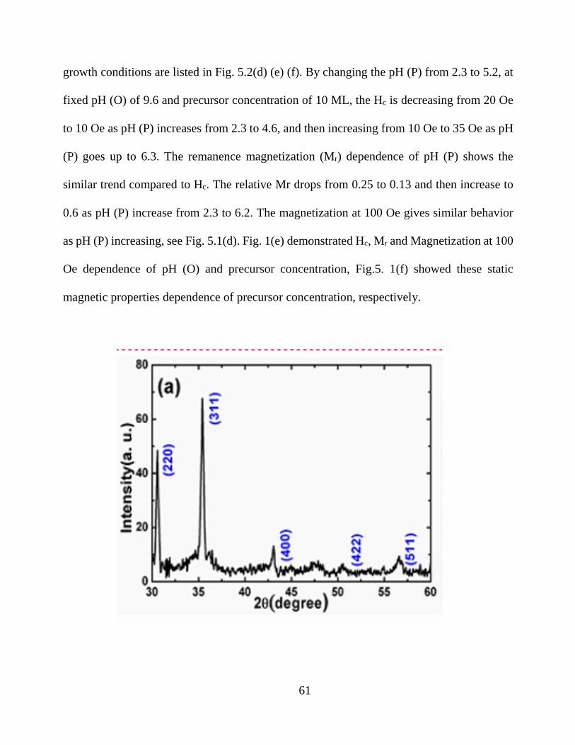
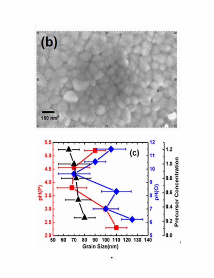
A typical spinel ferrite XRD pattern is given in Fig. 51(a), showing a pure polycrystalline
phase of Ni0.27Zn0.1Fe2.63O4 thin film. The composition of NiZn ferrite film has large
permeability compared with others.3The growth condition here, of this NiZn ferrite film, is
59
pH of precursor 4.5, pH of oxidizer 9.8, 10 ML precursor concentration. Fig. 5.1(b) shows
SEM images of NiZn ferrite of same growth condition; tightly packed atoms structure with
grain size of ~70 nm is confirmed. The roughness of this NiZn ferrite film is around 50 nm
with zero stress patterns (cracks) and growth defects present on the surface of the NiZn films.
By varying the growth conditions, like pH value of precursor and oxidizer, precursor
concentration, the grain size is changing, as given by Fig. 5.1(c). Red line gives the grain
size, with error bar of ~10 nm, dependence of pH value of precursor (pH (P)), fixing the pH
of oxidizer (pH (O)) as 9.6 and precursor concentration of 10 ML. Largest grain size of 110
nm was obtained at pH (P) = 2.2 and at pH (P) = 3.8, the smallest grain size is achieved as
68 nm. The blue line shows the grain size varying by pH (O) with fixed pH (P) = 4.6 and
precursor concentration of 10 ML. The grain size is relatively large, 125nm at pH (O) = 6.2,
105 nm at pH (O)=11.6, however, small of 70 nm at pH (O)=9.6. At last, the precursor
concentration(10 ML as 1, Y axis of precursor concentration, from 0.25 to 1.2, indicates the
proportion compared to 10 ML, for instance, 1.2 means precursor concentration of 12 ML)
have little influence to the grain size, as shown in Fig. 1(c). Figure 5.1(d) shows the atom
force microscopy (AFM) image of NiZn ferrite thin film, same growth condition with SEM
image sample.
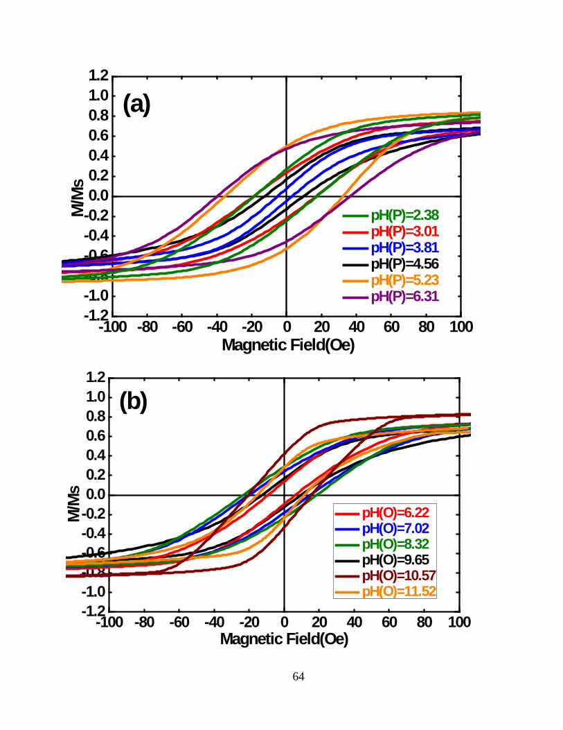
The M-H loops of NiZn ferrite films made under varying growth conditions is examined by
VSM, see Fig. 5.2. As demonstrated, the M-H loops of varying pH (P), pH (O) and precursor
concentration is showed in Fig. 5.2(a), (b), (c). Coercivity field (Hc), Remanence
Magnetization (Mr) and Magnetization at applied magnetic field of 100 Oe dependence of
60
growth conditions are listed in Fig. 5.2(d) (e) (f). By changing the pH (P) from 2.3 to 5.2, at
fixed pH (O) of 9.6 and precursor concentration of 10 ML, the Hc is decreasing from 20 Oe
to 10 Oe as pH (P) increases from 2.3 to 4.6, and then increasing from 10 Oe to 35 Oe as pH
(P) goes up to 6.3. The remanence magnetization (Mr) dependence of pH (P) shows the
similar trend compared to Hc. The relative Mr drops from 0.25 to 0.13 and then increase to
0.6 as pH (P) increase from 2.3 to 6.2. The magnetization at 100 Oe gives similar behavior
as pH (P) increasing, see Fig. 5.1(d). Fig. 1(e) demonstrated Hc, Mr and Magnetization at 100
Oe dependence of pH (O) and precursor concentration, Fig.5. 1(f) showed these static
magnetic properties dependence of precursor concentration, respectively.
61
62
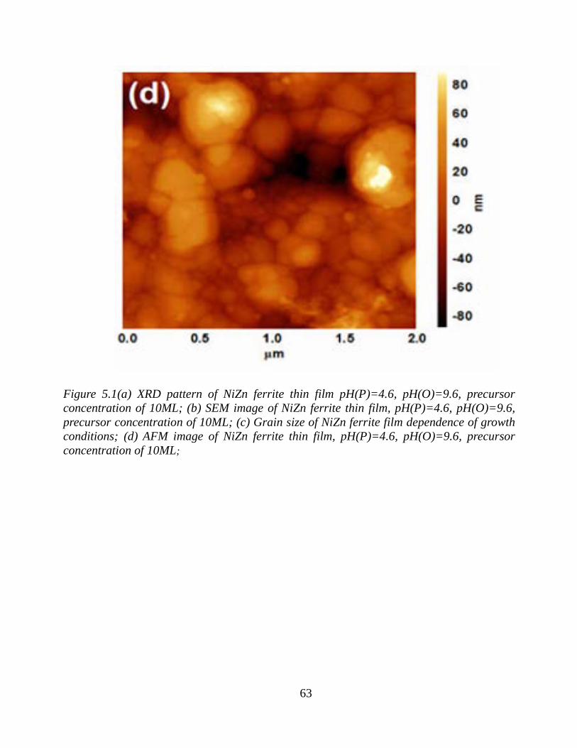
Figure 5.1(a) XRD pattern of NiZn ferrite thin film pH(P)=4.6, pH(O)=9.6, precursor concentration of 10ML; (b) SEM image of NiZn ferrite thin film, pH(P)=4.6, pH(O)=9.6, precursor concentration of 10ML; (c) Grain size of NiZn ferrite film dependence of growth conditions; (d) AFM image of NiZn ferrite thin film, pH(P)=4.6, pH(O)=9.6, precursor concentration of 10ML;
63
-100 -80 -60 -40 -20 0 20 40 60 80 100-1.2-1.0-0.8-0.6-0.4-0.20.00.20.40.60.81.01.2
pH(P)=2.38 pH(P)=3.01 pH(P)=3.81 pH(P)=4.56 pH(P)=5.23 pH(P)=6.31
M/M
s
Magnetic Field(Oe)
(a)
-100 -80 -60 -40 -20 0 20 40 60 80 100-1.2-1.0-0.8-0.6-0.4-0.20.00.20.40.60.81.01.2
(b)
M/M
s
Magnetic Field(Oe)
pH(O)=6.22 pH(O)=7.02 pH(O)=8.32 pH(O)=9.65 pH(O)=10.57 pH(O)=11.52
64
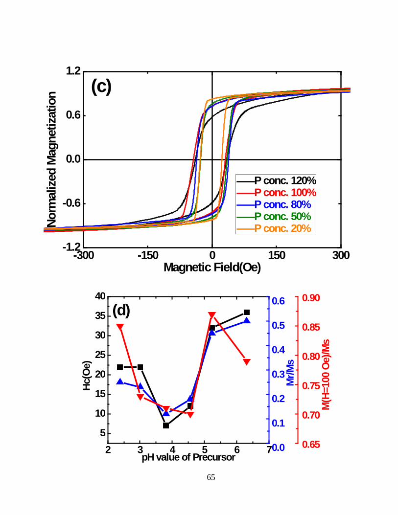
-300 -150 0 150 300-1.2
-0.6
0.0
0.6
1.2
No
rmal
ized
Mag
netiz
atio
n
Magnetic Field(Oe)
P conc. 120%P conc. 100%P conc. 80%P conc. 50%P conc. 20%
(c)
2 3 4 5 6 7
5
10
15
20
25
30
35
40
Hc(O
e)
pH value of Precursor0.0
0.1
0.2
0.3
0.4
0.5
0.6 M
r/Ms
0.65
0.70
0.75
0.80
0.85
0.90
M(H
=100
Oe)
/Ms
(d)
65

6 7 8 9 10 11 128
10
12
14
16
18
20
Hc(O
e)
pH value of Oxidizer
(e)
0.1
0.2
0.3
0.4
0.5
Mr/M
s
0.680.700.720.740.760.780.800.820.84
M(H
=100
Oe)
0.2 0.4 0.6 0.8 1.0 1.220
25
30
35
40
H c(O
e)
Precursor Concentration
0.5
0.6
0.7
0.8
0.9
1.0 M
r/Ms
(f)
0.0
0.2
0.4
0.6
0.8
1.0
M(H
=100
Oe)
/Ms
Figure 5.2 (a) M-H loops of varying pH(P) at fixed pH(O) and precursor concentration; (b) M-H loops of varying pH(O) at fixed pH(P) and precursor concentration; (c) M-H loops of varying precursor concentration at fixed pH(P) and pH(O); (d) Hc, Mr, Magnetization at 100Oe dependence of pH(P); (e) Hc, Mr, Magnetization at 100Oe dependence of pH(O); (f) Hc, Mr, Magnetization at 100Oe dependence of precursor concentration;
66
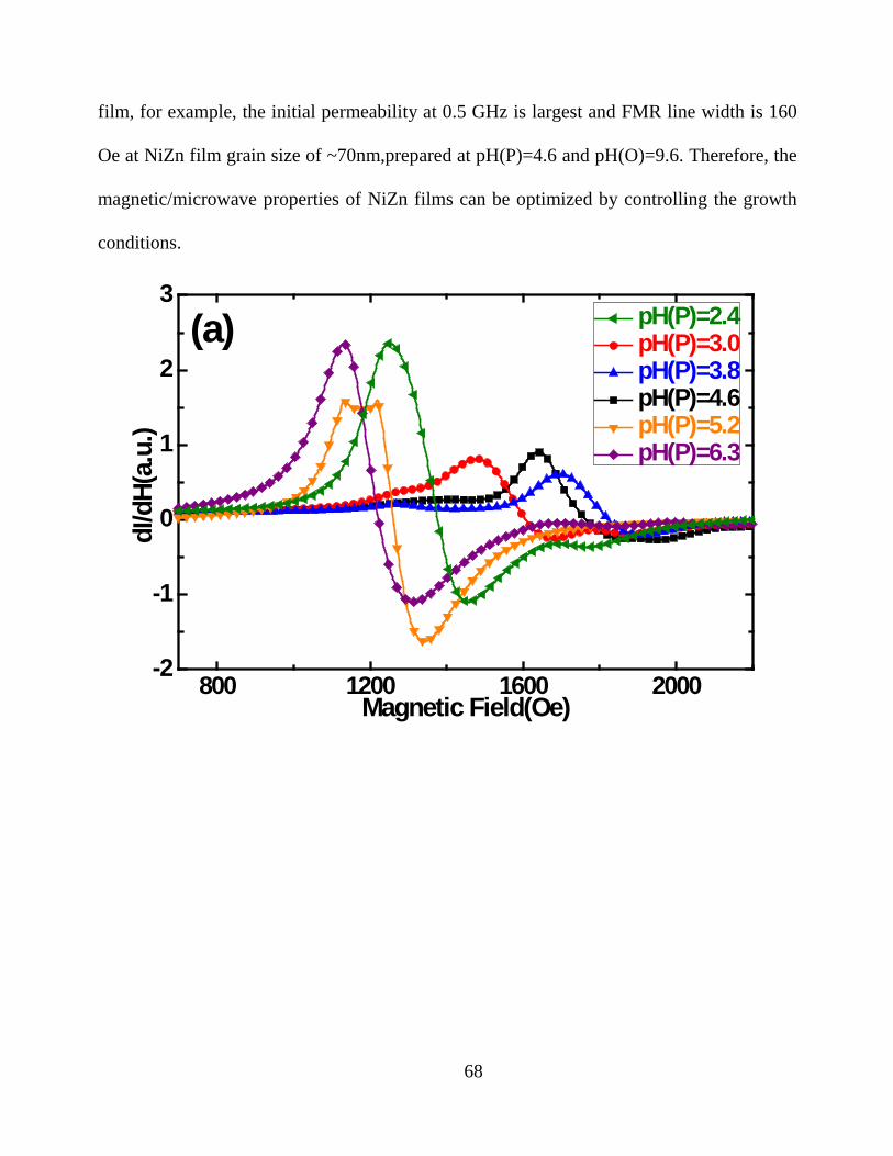
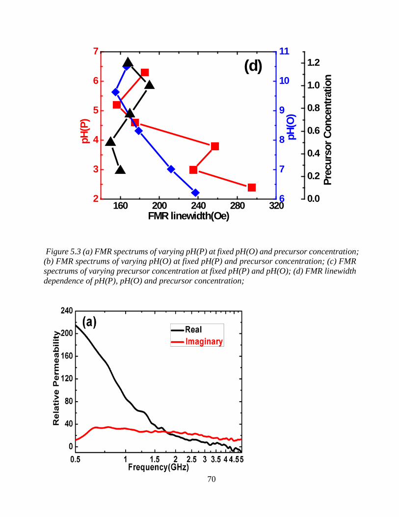
The FMR spectrums of NiZn film prepared by varying growth condition was investigated
on Fig. 5.3(a)(b)(c). The linewidth of FMR spectrum are listed in Fig. 5.3(d), varying with
growth conditions. The minimum FMR linewidth of 160 Oe is obtained at pH (P) = 4.6 and
pH (O)=9.6, which is important to RF/microwave application devices. Nevertheless, the
FMR linewidth changed little with varying concentration. Fig. 5.4(a) represents the
permeability spectra of NiZn ferrite film fabricated at pH (P) =4 .6, pH (O)=9.6 and precursor
concentration of 10ML. Large initial real permeability μr’>200 was achieved at 0.5 GHz,
μr’>80 at 1 GHz(~80 times larger than bulk NiZn ferrite)3 and with low loss tanδm
(μr”/μr’)<0.03 at 3-5GHz range. In Fig. 5.4(b), the initial permeability at 0.5 GHz dependence
of growth condition is studied, the NiZn ferrite film with maximum μr’ is obtained at pH (P)
=4.6, pH (O) =9.6, and precursor concentration of 10ML. The highest initial permeability is
optimized by varying growth condition, and further the highest resistivity is also obtained at
pH (P) =4.6, pH (O) =9.6, giving the good RF/microwave property in real devices. In our
experiment, static magnetic properties, Hc, Mr, and dynamic magnetic properties, FMR
linewidth, permeability, are changing as growth condition significantly. The reason may be
by adjusting the pH value of growth solution, the grain size of NiZn films can be easily
manipulated, therefore, tuning the static/dynamic magnetic properties. As shown in Fig.
5.1(c), the grain size d is decreasing from d>100 nm to ~70 nm as pH (P) increasing from 2.3
to 4.6, pH (O) increasing from 6.2 to 9.6. After pH (P), pH (O) increased to 6.2, 11.5
correspondingly, the grain size d increase to d>100 nm again. Grain size of NiZn films is
independent with precursor concentration basically; see Fig. 5.1(c). The trends of grain size
dependence of growth condition are similar to these magnetic/microwave property of NiZn
67
film, for example, the initial permeability at 0.5 GHz is largest and FMR line width is 160
Oe at NiZn film grain size of ~70nm,prepared at pH(P)=4.6 and pH(O)=9.6. Therefore, the
magnetic/microwave properties of NiZn films can be optimized by controlling the growth
conditions.
800 1200 1600 2000-2
-1
0
1
2
3
dI/d
H(a.
u.)
Magnetic Field(Oe)
pH(P)=2.4 pH(P)=3.0 pH(P)=3.8 pH(P)=4.6 pH(P)=5.2 pH(P)=6.3
(a)
68
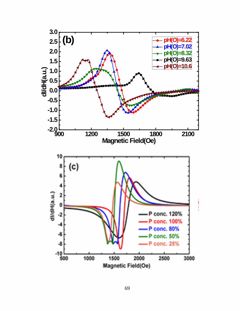
900 1200 1500 1800 2100-2.0-1.5-1.0-0.50.00.51.01.52.02.53.0
dI/d
H(a.
u.)
Magnetic Field(Oe)
pH(O)=6.22 pH(O)=7.02 pH(O)=8.32 pH(O)=9.63 pH(O)=10.6
(b)
69
160 200 240 280 3202
3
4
5
6
7
pH(P
)
FMR linewidth(Oe)6
7
8
9
10
11
pH(
O)
(d)
0.0
0.2
0.4
0.6
0.8
1.0
1.2
Pre
curs
or C
once
ntra
tion
Figure 5.3 (a) FMR spectrums of varying pH(P) at fixed pH(O) and precursor concentration; (b) FMR spectrums of varying pH(O) at fixed pH(P) and precursor concentration; (c) FMR spectrums of varying precursor concentration at fixed pH(P) and pH(O); (d) FMR linewidth dependence of pH(P), pH(O) and precursor concentration;
70
Figure 5.4 (a) Permeability spectrum of NiZn thin film with pH(P)=4.6, pH(O)=9.6 and precursor concentration of 10ML; (b) Permeability at 0.5 GHz of varying pH(P), pH(O) and precursor concentration; (c) Resistivity of NiZn films at varying pH(P), pH(O) and precursor concentration;
71
5.4 Conclusion
Controlling the growth condition of spin spray deposited NiZn ferrite thin film, the
microstructure of NiZn thin film can be achieved; therefore, the magnetic/microwave
properties of NiZn films can be optimized to fit the requirement of RF/microwave devices.
The real permeability of >200 at 0.5 GHz and loss of <0.03 at 3-5 GHz with FMR linewidth
of 160 Oe was realized. These properties are very useful for EMI suppression and also
applicable to RF/microwave devices like antennas, inductors in the GHz range.
72
Chapter. 6 Conclusion and future work 6.1. Conclusion In summary, we have demonstrated large FMR tunability through E-field induced, strain
mediated ME coupling in FeGaB/PIN-PMN-PT multiferroic composites. A large effective
magnetic anisotropy field change of 180 Oe was obtained, comparable to that of the
composites based on PMN-PT and PZN-PT. operational E-field range is -6.7 to 11 kV/cm,
almost double the range for PMN-PT and PZN-PT-based multiferroic composites. With a
high phase transition temperature TRT >120 °C for PIN-PMN-PT, FeGaB/PIN-PMN-PT
heterostructures have great potential for high-power tunable RF/microwave device
application with wider temperature operational range. Moreover, charge mediated ME
coupling in NiFe/PLZT multiferroic composites. A large effective magnetic anisotropy field
change of 70 Oe was obtained, comparable to that of the composites based on STO and MgO
operational E-field range is -300 to 300 kV/cm. With a large tunability for PLZT, NiFe/PLZT
heterostructures have great potential for high-power tunable RF/microwave device
application with wider temperature operational range.
More work was performed with multiferroics heterostructure fabricated with low temperature
controlling the growth condition of spin spray deposited NiZn ferrite thin film, the
microstructure of NiZn thin film can be achieved; therefore, the magnetic/microwave
properties of NiZn films can be optimized to fit the requirement of RF/microwave devices.
73
The real permeability of >200 at 0.5 GHz and loss of <0.03 at 3-5 GHz with FMR linewidth
of 160 Oe was realized. These properties are very useful for EMI suppression and also
applicable to RF/microwave devices like antennas, inductors in the GHz range.
6.2. Future Plan
6.2.1. Co-existence of strain and charge mediated magnetoelectric coupling for non-
volatile control of magnetism
Strong magnetoelectric coupling has been demonstrated in magnetic/dielectric or
magnetic/ferroelectric thin film heterostructures through a voltage controllable magnetic
surface anisotropy mediated by spin polarized charge.28,37-39,74-76 Combined strain-
mediated and charge-mediated magnetoelectric coupling is expected in ultra-thin
magnetic film/ferroelectric slabs, which has the potential for achieving even stronger
magnetoelectric coupling. For example, a multiferroic heterostructure with a magnetic
semiconductor, 4nm La0.8Sr0.2MnO3, on PZT produced a hysteretic-like M-E curve at 100
K due to a charge mediated magnetoelectric coupling; while a characteristic strain- mediated piezoelectric “butterfly” like M-E curve was observed in a heterostructure with50
nm La0.7Sr0.3MnO3 on PMN-PT. Shu et al. reported a thickness-dependent M-E
behavior in Ni/BTO multiferroic heterostructures through the voltage controlled
magneto-optical Kerr signal, where the charge-mediated magnetic surface anisotropy
increasingly dominates over the magnetoelastic anisotropy when decreasing the thickness of
Ni thin film down to 5 nm41. It is however difficult to separate the strain mediated
74
magnetic coupling from the charge mediated
magnetic coupling in such ultra-thin magnetic films on ferroelectric substrates. This is
due to the weak magnetic signal that results from the ultra-thin film; and there has been
no report of the precise measurements of the strain and charge co-mediated magnetoelectric
coupling.
By distinguishing the strain and surface charge magnetoelectric effect strength, the
hysteretic loop like M-E curve, in which the voltage controlled switch of the
magnetization corresponds to the switch of the ferroelectric polarization may be obtained.
The co-existence of strain and charge mediated magnetoelectric coupling in ultra-thin
magnetic/ferroelectric heterostructures could lead to non-volatile magnetoelectric devices
with significantly enhanced magnetoelectric coupling.
6.2.2. Power Efficient Tunable Inductors for RFIC
Strong magnetoelectric (ME) coupling has been demonstrated in
magnetostrictive/piezoelectric magnetoelectric heterostructures, which has enabled
different novel magnetoelectric devices, including magnetoelectric sensors, spintronics,
voltage tunable microwave magnetoelectric devices, etc. Exciting progress has been made
recently on power efficient tunable inductors, which have very high quality factor and
inductance with large tunability of inductance based on magnetic control of electrical
polarization in magnetic/piezoelectric magnetoelectric heterostructures. MEMS tunable
inductors were reported104-112. Tunable inductors are classified into two main groups:
75

discrete type and continuous type. Each of these groups is itself classified into other types
based on tuning mechanism, actuation mechanism and so on. The discrete type tunable
inductors are those whose inductance changes digitally employing series-parallel inductors
concept, magnetic coupling coefficient concept, and CPW lines concept. The continuous
type tunable inductors work based on continuously inductance changing and categorized
into different types such as core properties changing concept, mutual inductance based
inductors, store magnetic energy based inductors, and so on. Some properties of tunable
inductors such as quality factor, tuning range, actuation voltage, etc. are investigated. Large
tuning range are very difficult to reach. I propose that, by using magnetioelectric coupling,
the tuning of inductor can be easily to control by applying electrical field.
76
References
1 Fiebig, M. Revival of the magnetoelectric effect. Journal of Physics D: Applied
Physics 38, R123-R152, (2005).
2 Bibes, M. & Barthelemy, A. Multiferroics: Towards a magnetoelectric memory.
Nature materials 7, 425-426, (2008).
3 Nan, C. W., Bichurin, M. I., Dong, S. X., Viehland, D. & Srinivasan, G. Multiferroic
magnetoelectric composites: Historical perspective, status, and future directions. Journal of
Applied Physics 103, 2836410 (2008).
4 Ma, J., Hu, J., Li, Z. & Nan, C. W. Recent progress in multiferroic magnetoelectric
composites: from bulk to thin films. Adv Mater 23, 1062-1087, (2011).
5 Spaldin, N. A., Cheong, S. W. & Ramesh, R. Multiferroics: Past, present, and future.
Physics Today 63, 38-43 (2010).
6 Ramesh, R. & Spaldin, N. A. Multiferroics: progress and prospects in thin films.
Nature materials 6, 21-29, (2007).
7 Vaz, C. A. Electric field control of magnetism in multiferroic heterostructures. Journal
of physics. Condensed matter : an Institute of Physics journal 24, 333201, (2012).
8 Sun, N. X. & Srinivasan, G. Voltage Control of Magnetism in Multiferroic
Heterostructures and Devices. Spin 02, 1240004, (2012).
9 Ma, J., Hu, J. M., Li, Z. & Nan, C. W. Recent Progress in Multiferroic Magnetoelectric
Composites: from Bulk to Thin Films. Advanced Materials 23, 1062-1087, (2011).
10 Martin, L. W. et al. Multiferroics and magnetoelectrics: thin films and nanostructures.
77
Journal of Physics: Condensed Matter 20, 434220, (2008).
11 Dong, S., Cheng, J., Li, J. F. & Viehland, D. Enhanced magnetoelectric effects in
laminate composites of Terfenol-D/Pb(Zr,Ti)O3 under resonant drive. Applied Physics
Letters 83, 4812, (2003).
12 Dong, S., Li, J. F., Viehland, D., Cheng, J. & Cross, L. E. A strong magnetoelectric
voltage gain effect in magnetostrictive-piezoelectric composite. Applied Physics Letters 85,
3534, (2004).
13 Dong, S., Zhai, J., Li, J. & Viehland, D. Small dc magnetic field response of
magnetoelectric laminate composites. Applied Physics Letters 88, 082907, (2006).
14 Greve, H., Woltermann, E., Quenzer, H.-J., Wagner, B. & Quandt, E. Giant
magnetoelectric coefficients in (FeCoSiB-AlN thin film composites. Applied Physics Letters
96, 182501, (2010).
15 Marauska, S. et al. MEMS magnetic field sensor based on magnetoelectric
composites. Journal of Micromechanics and Microengineering 22, 065024, (2012).
16 Lou, J. et al. in 2009 Ieee/Mtt-S International Microwave Symposium, Vols 1-3 IEEE
MTT-S International Microwave Symposium 33-36 (Ieee, 2009).
17 Liu, M. et al. Voltage tuning of ferromagnetic resonance with bistable magnetization
switching in energy-efficient magnetoelectric composites. Adv Mater 25, 1435-1439, (2013).
18 Semenov, A. A. et al. Ferrite-ferroelectric layered structures for electrically and
magnetically tunable microwave resonators. Applied Physics Letters 88, 033503, (2006).
19 Fetisov, Y. K. & Srinivasan, G. Electric field tuning characteristics of a ferrite-
piezoelectric microwave resonator. Applied Physics Letters 88, 2191950 (2006).
78
20 Liu, M., Lou, J., Li, S. D. & Sun, N. X. E-Field Control of Exchange Bias and
Deterministic Magnetization Switching in AFM/FM/FE Multiferroic Heterostructures.
Advanced Functional Materials 21, 2593-2598, (2011).
21 Zhai, J. Y. et al. Tunable magnetoelectric resonance devices. Journal of Physics D:
Applied Physics 42, 122001, (2009).
22 Wang, J. et al. Epitaxial BiFeO3 multiferroic thin film heterostructures. Science
299, 1719-1722, (2003).
23 Martin, L. W. et al. Nanoscale control of exchange bias with BiFeO3 thin films.
Nano letters 8, 2050-2055 (2008).
24 Chu, Y. H. et al. Electric-field control of local ferromagnetism using a magnetoelectric
multiferroic. Nature materials 7, 478-482, (2008).
25 Lim, S. H. et al. Exchange bias in thin-film (Co/Pt)3/Cr2O3 multilayers. Journal of
Magnetism and Magnetic Materials 321, 1955-1958, (2009).
26 Prellier, W., Singh, M. P. & Murugavel, P. The single-phase multiferroic oxides: from
bulk to thin film. Journal of Physics: Condensed Matter 17, R803-R832, (2005).
27 Das, J., Song, Y. Y., Mo, N., Krivosik, P. & Patton, C. E. Electric-Field-Tunable Low
Loss Multiferroic Ferrimagnetic-Ferroelectric Heterostructures. Advanced Materials 21,
2045-2049, (2009).
28 Shiota, Y. et al. Quantitative Evaluation of Voltage-Induced Magnetic Anisotropy
Change by Magnetoresistance Measurement. Applied Physics Express 4, 043005, (2011).
29 Maruyama, T. et al. Large voltage-induced magnetic anisotropy change in a few
atomic layers of iron. Nature nanotechnology 4, 158-161, (2009).
79
30 Tulapurkar, A. A. et al. Spin-torque diode effect in magnetic tunnel junctions.
Nature 438, 339-342, (2005).
31 Hu, J.-M. & Nan, C. W. Electric-field-induced magnetic easy-axis reorientation in
ferromagnetic/ferroelectric layered heterostructures. Physical Review B 80, 224416 (2009).
32 Hu, J.-M., Li, Z., Chen, L.-Q. & Nan, C.-W. High-density magnetoresistive random
access memory operating at ultralow voltage at room temperature. Nature communications
2, 553, (2011).
33 Hu, J.-M., Li, Z., Chen, L.-Q. & Nan, C.-W. Design of a Voltage-Controlled
Magnetic Random Access Memory Based on Anisotropic Magnetoresistance in a Single
Magnetic Layer. Advanced Materials 24, 2869-2873, (2012).
34 Zheng, H. et al. Multiferroic BaTiO3-CoFe2O4 Nanostructures. Science 303, 661-
663, (2004).
35 Lou, J., Liu, M., Reed, D., Ren, Y. H. & Sun, N. X. Giant Electric Field Tuning of
Magnetism in Novel Multiferroic FeGaB/Lead Zinc Niobate-Lead Titanate (PZN- PT)
Heterostructures. Advanced Materials 21, 4711 (2009).
36 Lou, J. et al. Soft magnetism, magnetostriction, and microwave properties of FeGaB
thin films. Applied Physics Letters 91, 2804123 (2007).
37 Weisheit, M. et al. Electric field-induced modification of magnetism in thin-film
ferromagnets. Science 315, 349-351, (2007).
38 Duan, C.-G. et al. Surface Magnetoelectric Effect in Ferromagnetic Metal Films.
Physical Review Letters 101, 137201 (2008).
39 Duan, C.-G., Jaswal, S. & Tsymbal, E. Predicted Magnetoelectric Effect in Fe/BaTiO3
80
Multilayers: Ferroelectric Control of Magnetism. Physical Review Letters 97, (2006).
40 Duan, C.-G. et al. Tailoring magnetic anisotropy at the ferromagnetic/ferroelectric
interface. Applied Physics Letters 92, 122905, (2008).
41 Shu, L. et al. Thickness-dependent voltage-modulated magnetism in multiferroic
heterostructures. Applied Physics Letters 100, 022405-022404 (2012).
42 Zhou, Z. et al. Quantifying thickness-dependent charge mediated magnetoelectric
coupling in magnetic/dielectric thin film heterostructures. Applied Physics Letters 103,
232906, (2013).
43 Garcia, V. et al. Ferroelectric control of spin polarization. Science 327, 1106-1110,
(2010).
44 Meng, H. et al. Electric field effects in low resistance CoFeB-MgO magnetic tunnel
junctions with perpendicular anisotropy. Applied Physics Letters 100, 122405, (2012).
45 Prokhnenko, O. et al. Enhanced Ferroelectric Polarization by Induced Dy Spin Order
in Multiferroic DyMnO3. Physical Review Letters 98, 98.057206 (2007).
46 He, X. et al. Robust isothermal electric control of exchange bias at room temperature.
Nature materials 9, 579-585, (2010).
47 He, Q. et al. Electrically controllable spontaneous magnetism in nanoscale mixed
phase multiferroics. Nature communications 2, 225, (2011).
48 Zhao, T. et al. Electrical control of antiferromagnetic domains in multiferroic BiFeO3
films at room temperature. Nature materials 5, 823-829, (2006).
49. G. Subramanyam, M. W. Cole, N. X. Sun, T. S. Kalkur, N. M. Sbrockey, G. S. Tompa,
X. Guo, C. Chen, S. P. Alpay, G. A. Rossetti, K. Dayal, L.-Q. Chen and D. G. Schlom,
81
Journal of Applied Physics 114 (19), 191301 (2013).
50. N. X. Sun and G. Srinivasan, Spin 02 (03), 1240004 (2012).
51. M. Liu and N. X. Sun, Philosophical Transactions of the Royal Society A: Mathematical,
Physical and Engineering Sciences 372 (2009), 20120439-20120439 (2014).
52. W. Eerenstein, N. D. Mathur, and J. F. Scott, Nature 442, 759 (2006).
53.C. W. Nan, M. I. Bichurin, S. X. Dong, D. Viehland, and G. Srinivasan, J. Appl. Phys.
103, 031101 (2008).
54. C. A. F. Vaz, J. Hoffman, C. H. Ahn, and R. Ramesh, Adv. Mater. 22, 2900–2918
(2010).
55. L. W. Martin, S. P. Crane, Y. H. Chu, M. B. Holcomb, M. Gajek, M. Huijben, C. H.
Yang, N. Balke, and R. Ramesh, J. Phys.: Condens. Matter 20, 434220 (2008).
57. N. X. Sun and G. Srinivasan, Spine 2, 1240004 (2012).
58. Y. K. Fetisov and G. Srinivasana, Appl. Phys. Lett. 88, 143503 (2006). 7T. X. Nan, Y.
Hui, M. Rinaldi, and N. X. Sun, Sci. Rep. 3, 1985 (2013). 8M. Bibes and A. Barthelemy,
Nature Mater. 7, 425–426 (2008).
59. X. Yang, J. Wu, S. Beguhn, T. Nan, Y. Gao, Z. Zhou, and N. X. Sun, IEEE Microw.
Wirel. Compon. Lett. 23, 184 (2013).
60. X. Yang, Y. Gao, J. Wu, S. Beguhn, T. Nan, Z. Zhou, M. Liu, and N. X. Sun, IEEE Trans.
Magn. 49, 5485 (2013).
61. S. Li, M. Liu, W. Shao, J. Xu, S. Chen, Z. Zhou, T. Nan, N. X. Sun, and J. G. Duh, J.
Appl. Phys. 113, 17C727 (2013).
62. Z. Zhou, S. Beguhn, J. Lou, S. Rand, M. Li, X. Yang, S. D. Li, M. Liu,
82
and N. X. Sun, J. Appl. Phys. 111, 103915 (2012).
63. T. X. Nan, Z. Zhou, J. Lou, M. Liu, X. Yang, Y. Gao, S. Rand, and N. X. Sun, Appl.
Phys. Lett. 100, 132409 (2012).
64. M. Liu, Z. Zhou, T. X. Nan, B. M. Howe, G. J. Brown, and N. X. Sun,
Adv. Mater. 25, 1435 (2013).
65. M. Liu, S. D. Li, Z. Zhou, S. Beguhn, J. Lou, F. Xu, T. J. Lu, and N. X. Sun, J. Appl.
Phys. 112, 063917 (2012)
66. M. Li, Z. Zhou, M. Liu, J. Lou, D. E. Oates, G. F. Dionne, M. L. Wang, and N. X. Sun,
J. Phys. D: Appl. Phys. 46, 275001 (2013)
67. H. Greve, E. Woltermann, H. J. Quenzer, B. Wagner, and E. Quandt, Appl. Phys. Lett.
96, 182501 (2010)
68. P. Zhao, Z. L. Zhao, D. Hunter, R. Suchoski, C. Gao, S. Mathews, M. Wuttig, and I.
Takeuchi, Appl. Phys. Lett. 94, 243507 (2009).
69. C. G. Duan, J. P. Velev, R. F. Sabirianov, Z. Q. Zhu, J. H. Chu, S. S.
Jaswal, and E. Y. Tsymbal, Phys. Rev. Lett. 101, 137201 (2008).
70. C. G. Duan, S. S. Jaswal, and E. Y. Tsymbal, Phys. Rev. Lett. 97, 047201 (2006)
71. M. K. Niranjan, C. G. Duan, S. S. Jaswal, and E. Y. Tsymbal, Appl. Phys. Lett. 96,
222504 (2010).
72. J. M. Rondinelli, M. Stengel, and N. A. Spaldin, Nat. Nanotechnol. 3, 46–50 (2008)
73. H. J. A. Molegraaf, J. Hoffman, C. A. F. Vaz, S. Gariglio, D. van der Marel, C. H. Ahn,
and J. M. Triscone, Adv. Mater. 21, 3470 (2009).
74. C. A. F. Vaz, J. Hoffman, Y. Segal, J. W. Reiner, R. D. Grober, Z. Zhang, C. H. Ahn,
83
and F. J. Walker, Phys. Rev. Lett. 104, 127202 (2010).
75. Z. Li, J. M. Hu, L. Shu, Y. Gao, Y. Shen, Y. H. Lin, and C. W. Nan, J. Appl. Phys. 111,
033918 (2012).
76. L. Shu, Z. Li, J. Ma, Y. Gao, L. Gu, Y. Shen, Y. H. Lin, and C. W. Nan, Appl. Phys. Lett.
100, 022405 (2012).
77. T. Maruyama, Y. Shiota, T. Nozaki, K. Ohta, N. Toda, M. Mizuguchi, A. A. Tulapurkar,
T. Shinjo, M. Shiraishi, S. Mizukami, Y. Ando, and Y. Suzuki, Nat. Nanotechnol. 04, 158
(2009).
78. Y. Shiota, T. Maruyama, T. Nozaki, T. Shinjo, M. Shiraishi, and Y.Suzuki, Appl.
Phys. Express 2, 063001 (2009).
79. S. S. Ha, N. H. Kim, S. Lee, C. Y. You, Y. Shiota, T. Maruyama, T. Nozaki, and Y.
Suzuki, Appl. Phys. Lett. 96, 142512 (2010).
80. U. Bauer, M. Przybylski, J. Kirschner, and G. S. D. Beach, Nano Lett. 12, 1437–1442
(2012).
82. Y. Shiota, S. Murakami, F. Bonell, T. Nozaki, T. Shinjo, and Y. Suzuki, Appl. Phys.
Express 4, 043005 (2011).
83. J. T. Heron, M. Trassin, K. Ashraf, M. Gajek, Q. He, S. Y. Yang, D. E. Nikonov, Y. H.
Chu, S. Salahuddin, and R. Ramesh, Phys. Rev. Lett. 107, 217202 (2011).
84. T. Zhao, A. Scholl, F. Zavaliche, K. Lee, M. Barry, A. Doran, M. P. Cruz, Y. H. Chu, C.
Ederer, N. A. Spaldin, R. R. Das, D. M. Kim, S. H. Baek, C. B. Eom, and R. Ramesh, Nature
Mater. 5, 823–829 (2006).
85. Y. H. Chu, Q. Zhan, L. W. Martin, M. P. Cruz, P. L. Yang, G. W. Pabst, F. Zavaliche, S.
84
Y. Yang, J. X. Zhang, L. Q. Chen, D. G. Schlom, I. N. Lin, T. B. Wu, and R. Ramesh, Adv.
Mater. 18, 2307–2311 (2006).
86. Y.-Hao Chu, Q. He, C.-Ho Yang, P. Yu, L. W. Martin, P. Shafer, and R. Ramesh, Nano
Lett. 9(4), 1726–1730 (2009).
87. S. H. Baek, H. W. Jang, C. M. Folkman, Y. L. Li, B. Winchester, J. X. Zhang, Q. He, Y.
H. Chu, C. T. Nelson, M. S. Rzchowski, X. Q. Pan, R. Ramesh, L. Q. Chen, and C. B. Eomm,
Nature Mater. 9, 309 (2010).
88. S. M. Wu, S. A. Cybart, P. Yu, M. D. Rossell, J. X. Zhang, R. Ramesh, and R. C. Dynes,
Nature Mater. 9, 756 (2010).
89. C. M. Fu, H. S. Hsu, Y. C. Chao, N. Matsushita, and M. Abe, J. Appl. Phys. 93, 7127
(2003)
90. N. Matsushita, T. Nakamura, and M. Abe, IEEE Trans. Magn. 38, 3111 (2002)
91. O. Obi, M. Liu, J. Lou, S. Stoute, X. Xing, N. X. Sun, J. Warzywoda, A. Sacco, D. E.
Oates, and G. F. Dionne, J. Appl. Phys. 109, 07E527 (2011)
92. M. Abe and Y. Tamaura, Jpn. J. Appl. Phys. 22, L511 (1983)
93. M. Liu, O. Obi, J. Lou, Y. Chen, Z. Cai, S. Stoute, M. Espanol, M. Lew, X. Situ, K. S.
Ziemer, V. G. Harris, and N. X. Sun, Adv. Funct. Mater. 19, 1826 (2009)
94. M. Liu, O. Obi, J. Lou, St. Stoute, J. Y. Huang, Z. Cai, K. S. Ziemer, and N. X. Sun,
Appl. Phys. Lett. 92, 152504 (2008)
95. K. Kondo, S. Yoshida, H. Ono, and M. Abe, J. Appl. Phys. 101, 09M502 (2007)
95. Y. Shimada, N. Matsushita, M. Abe, K. Kondo, T. Chiba, and S. Yoshida, J. Magn. Magn.
Mater. 278, 256 (2004)
85
97. G. M. Yang, X. Xing, A. Daigle, M. Liu, O. Obi, J. W. Wang, K. Naishadham, and N. X.
Sun, IEEE Trans. Magn. 44, 3091 (2008)
98. G. M. Yang, X. Xing, A. Daigle, O. Obi, M. Liu, J. Lou, S. Stoute, K. Naishadham, and
Nian X. Sun, IEEE Trans. Antennas Propag. 58, 648 (2010).
99. G. M. Yang, A. Shrabstein, X. Xing, O. Obi, S. Stoute, M. Liu, J. Lou, and N. X. Sun,
IEEE Trans. Magn. 45, 4191 (2009).
100. N. Matsushita, T. Nakamura, and M. Abe, J. Appl. Phys. 93, 7133 (2003).
101. Y. Ding, T. J. Klemmer, and T. M. Crawford, J. Appl. Phys., 96, 2969 (2004).
102. A. Fujiwara, M. Tada, T. Nakamura, and M. Abe, J. Magn. Magn. Mater. 320, L67
(2008).
103. Liu Chao , Anjali Sharma , Mohammed N. Afsar , Fellow, IEEE, Ogheneyunume Obi ,
Ziyao Zhou , and Nian Sun, IEEE TRANSACTIONS ON MAGNETICS, VOL. 48, NO.
11, NOVEMBER 2012
104. Dong-Ming Fang ,Hai-Xia Zhang, Norman C. Tien “A review of the tunable
microinductors”.
105. Mir Majid Teymoori and Jaber Merrikhi Ahangarkolaei “Mems Tunable Inductors: A
Survey” Australian Journal of Basic and Applied Sciences, 5(12): 1868-1878, 2011.
106. Mina Rais-Zadeh, Paul A. Kohl, and Farrokh Ayazi, “MEMS Switched Tunable
Inductors” JOURNAL OF MICROELECTROMECHANICAL SYSTEMS, VOL. 17, NO.
1, FEBRUARY 2008.
107. Marina Vroubel, Yan Zhuang, Behzad Rejaei, and Joachim N. Burghartz “Integrated
Tunable Magnetic RF Inductor” IEEE ELECTRON DEVICE LETTERS, VOL. 25, NO. 12,
86
DECEMBER 2004.
108. J. Lou, D. Reed, M. Liu, and N. X. Sun.”Electrostaticallay tunable magnetoelectric
inductor with large inductance tunability”. APPLIED PHYSICS LETTERS 94, 112508
(2009)
109. Kenichi Okada, Hirotaka Sugawara, Hiroyuki Ito, Kazuhisa Itoi, Masakazu Sato,
Hiroshi Abe, Tatsuya Ito, and Kazuya Masu. ” On-Chip High-Q Variable Inductor Using
Wafer-Level Chip-Scale Package Technology”, IEEE TRANSACTIONS ON ELECTRON
DEVICES, VOL. 53, NO. 9, SEPTEMBER 2006.
110. V. M. LUBECKE, B. BARBER, E.CHAN, D. LOPEZ, AND P. GAMMEL, “SELF-
ASSEMBLING MEMS VARIABLE AND FIXED RF INDUCTORS”.
111. N. X. Sun and G. Srinivasan, “Voltage Control of Magnetism in Multiferroic
Heterostructures and Devices,” Spin, Vol. 2, No. 3, 1240004 (46 pages), 2012
112. G. M. Rebeiz, K. Entesari, I. C. Reines, S. J. Park, M. A. El-Tanani, A. Grichener, and
A. R. Brown, “Tuning in to RF MEMS,” IEEE Microwave Magzine, Vol. 10, Issue. 6, pp.
55-72, 2009
113. Tianxiang Nan, Ziyao Zhou, Ming Liu, Xi Yang, Yuan Gao, and Nian X. Sun,
"Quantification of strain and charge co-mediated magnetoelectric coupling on ultra-thin
Permalloy/PMN-PT interface", Scientific Reports, 4, 3688 (2014).
87