Embed Size (px)
Citation preview
ORIGINAL PAPER Open Access
Structure and electrical properties of sputteredTiO2/ZrO2 bilayer composite dielectrics uponannealing in nitrogenMing Dong1, Hao Wang2*, Cong Ye2*, Liangping Shen2, Yi Wang2, Jieqiong Zhang2 and Yun Ye2
Abstract
The high-k dielectric TiO2/ZrO2 bilayer composite film was prepared on a Si substrate by radio frequencymagnetron sputtering and post annealing in N2 at various temperatures in the range of 573 K to 973 K.Transmission electron microscopy observation revealed that the bilayer film fully mixed together and had goodinterfacial property at 773 K. Metal-oxide-semiconductor capacitors with high-k gate dielectric TiO2/ZrO2/p-Si werefabricated using Pt as the top gate electrode and as the bottom side electrode. The largest property permittivity of46.1 and a very low leakage current density of 3.35 × 10⁻⁵ A/cm2 were achieved for the sample of TiO2/ZrO2/Siafter annealing at 773 K.
IntroductionHigh dielectric constant [high-k] materials have beenresearched for a few years in material science and havebeen applied firstly in Intel’s 45 nm MOSFET in 2007.Nowadays, for the demand of the next generationdevices for sub-22 nm technology nodes, expect thathigh-k materials such as HfO2, ZrO2, Ta2O5, and rareearth oxides are extensively researched, and binary oxi-des of high-k materials become more attractive and areexpected to be utilized in the future ultra large scaleintegrated circuit [1-8]. Among them, ZrO2 has a rela-tively high permittivity, large band gap, and good ther-mal and chemical stabilities. TiO2 is a high-k materialwith a very high permittivity of about 80 [9]. In order toimprove the permittivity of ZrO2, the feasible way is tofabricate ZrO2-TiO2 composite films. Meanwhile, as acomposite thin film, the addition of TiO2 can improvethe crystallization temperature [10,11]. As ZrO2-TiO2
binary oxides, a nanolaminate structure which can tailorthe electrical properties of dielectric stacks has manyapplications such as MIM diodes, storage capacitors,non-volatile memories, and transparent thin film transis-tors; thus, the nanolaminated ZrO2-TiO2 high dielectricconstant thin film is worth studying
Concerning high-k stacks on silicon, the interface hasan important role to influence the device. Normally, it isoften thought that TiO2 is easier to react with the Sisubstrate which may deteriorate the property of thedevice, and thus, TiO2/ZrO2/Si stacks may have betterelectrical characterization [12-14]. In the present work,metal-oxide-semiconductor [MOS] capacitors with high-k gate dielectric TiO2/ZrO2/p-Si were fabricated usingPt as the top gate electrode and as the bottom side elec-trode. The structure and electrical property of the TiO2/ZrO2/Si stack are studied.
Experimental detailsZrO2 and TiO2 thin films were grown onto p-type (100)Si (P~1015 cm-3) to fabricate TiO2/ZrO2/Si stacks byradio frequency magnetron sputtering at room tempera-ture. Pure ZrO2 (99.999%) and TiO2 (99.999%) ceramictargets (50 mm in diameter) were used as the sputteringtargets. The sputtering power of ZrO2 and TiO2 are 60W and 30 W, respectively. Pure argon (99.999%) with30 cm3/min flow rate controlled by a mass flow control-ler was used as sputtering gas, and the base pressure ofthe vacuum chamber is about 3 × 10⁻⁵ Pa. Sputteringwas carried out at a pressure of 0.3 Pa. As for thedeposited TiO2/ZrO2/Si stacks, post annealing of 573 K,773 K, and 973 K in N2 for 30 min was performed.The structural characteristics of the films were investi-
gated by X-ray diffraction [XRD] (Bruker D8, Bruker,
* Correspondence: [email protected]; [email protected] of Physics and Electronic Technology, Hubei University, Wuhan,430062, ChinaFull list of author information is available at the end of the article
Dong et al. Nanoscale Research Letters 2012, 7:31http://www.nanoscalereslett.com/content/7/1/31
© 2012 Dong et al; licensee Springer. This is an Open Access article distributed under the terms of the Creative Commons AttributionLicense (http://creativecommons.org/licenses/by/2.0), which permits unrestricted use, distribution, and reproduction in any medium,provided the original work is properly cited.
Billerica, MA, USA) and transmission electron micro-scopy [TEM] (FEI Tecnai G20, FEI Co., Hillsboro, OR,USA). Film thickness was determined by an ex situphase-modulated spectroscopic ellipsometry [SE] (ModelJobin Yvon, HORIBA Jobin Yvon Inc., Edison, NJ, USA)over the spectral range of 1.5 to 6.5 eV at an angle ofincidence of 70°. For the purpose of exploring electricalproperties, a Pt/TiO2/ZrO2/p-Si MOS capacitor was fab-ricated by sputtering a Pt top electrode with an area of1.96 × 10-7 m2 through a shadow mask. The back sideof the wafer was HF-cleaned, and the Pt thin film wasdeposited. The MOS capacitors were electrically charac-terized using a Radiant Precision Premier (RadiantTechnologies Inc., Albuquerque, NM, USA) tester sys-tem to obtain current-voltage [I-V] curves. Capacitance-voltage [C-V] measurements were performed by a preci-sion LCR meter (Agilent 4294A; Agilent TechnologiesInc., Santa Clara, CA, USA).
Results and discussionThe chemical composition of the TiO2/ZrO2/Si film canbe measured by XRF, and all samples have nearly thesame atomic Ti content of 21%, which indicates that theannealing process did not change the composition. Con-cerning the Ti content in the TiO2-ZrO2 binary system,the optimal content of about 21% has been verified inour previous work [10].Spectroscopic ellipsometry was employed to measure
the film thickness. The Tauc-Lorentz model which isespecially suitable for an amorphous material wasadopted to characterize the dielectric function of theTiO2/ZrO2 bilayer composite film [15-17]. In order toget the best fitting of SE data, different models werebuilt due to the structure change of the TiO2/ZrO2
bilayer composite film. For the as-deposited thin film, adouble layer optical model was built on Si (100) sub-strate, i.e., ZrO2 layer (L1) and TiO2 layer (L2), while forthe annealed one, only one layer of the ZrO2-TiO2
composite thin film was built. Lastly, we can obtain thethickness of the as-deposited thin film with a ZrO2 layer(L1) of 27.639 ± 0.521 nm and TiO2 layer (L2) of 10.077± 0.627 nm. For the sample annealed at 773 K, the totalthickness is 28.149 ± 1.102 nm. This result indicatesthat annealing makes the film denser and decreases thethickness.The detailed structure of the TiO2/ZrO2/Si film was
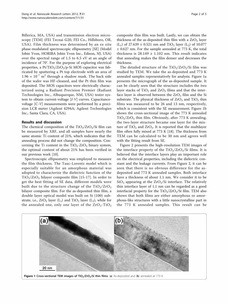
studied by TEM. We take the as-deposited and 773 Kannealed samples representatively for analysis. Figure 1apresents the micrograph of the as-deposited sample. Itcan be clearly seen that the structure includes the twolayer stacks of TiO2 and ZrO2 films and that the inter-face layer is observed between the ZrO2 film and the Sisubstrate. The physical thickness of ZrO2 and TiO2 thinfilms was measured to be 26 and 13 nm, respectively,which is consistent with the SE measurement. Figure 1bshows the cross-sectional image of the 773 K annealedTiO2/ZrO2 thin film. Obviously, after 773 K annealing,the two-layer structure became one layer for the mix-ture of TiO2 and ZrO2. It is reported that the multilayerfilm often fully mixed at 773 K [18]. The thickness fromTEM can be calculated to be 30 nm and agrees wellwith the fitting result from SE.Figure 2 presents the high-resolution TEM images of
the interface property of the TiO2/ZrO2/Si films. It isbelieved that the interface layers play an important roleon the electrical properties, including the dielectric con-stant and the leakage currents. From Figure 2, it can beseen that there is no obvious difference for the as-deposited and 773 K annealed samples. Both interfacehave a thickness of about 1.1 nm. We consider it to beSiO2 appearing at the ZrO2/Si interface. The relativelythin interface layer of 1.1 nm can be regarded as a goodinterfacial property for the TiO2/ZrO2/Si film. TEM alsoshows that both films are either amorphous or amor-phous-like structures with a little nanocrystalline part inthe 773 K annealed samples. This result can be
Figure 1 Cross-sectional TEM images of TiO2/ZrO2/Si thin films. (a) As-deposited and (b) annealed at 773 K.
Dong et al. Nanoscale Research Letters 2012, 7:31http://www.nanoscalereslett.com/content/7/1/31
Page 2 of 5
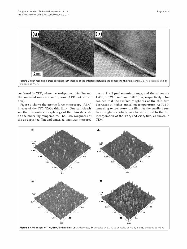
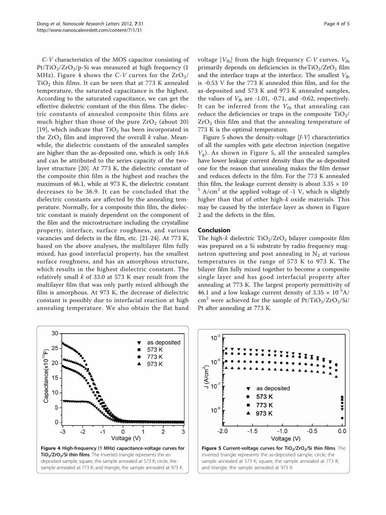
confirmed by XRD, where the as-deposited thin film andthe annealed ones are amorphous (XRD not shownhere).Figure 3 shows the atomic force microscopy [AFM]
images of the TiO2/ZrO2 thin films. One can clearlysee that the surface morphology of the films dependson the annealing temperature. The RMS roughness ofthe as-deposited film and annealed ones was measured
over a 2 × 2 μm2 scanning range, and the values are1.430, 1.529, 0.625 and 0.826 nm, respectively. Onecan see that the surface roughness of the thin filmdecreases at higher annealing temperature. At 773 Kannealing temperature, the film has the smallest sur-face roughness, which may be attributed to the fullincorporation of the TiO2 and ZrO2 film, as shown inTEM.
Figure 2 High-resolution cross-sectional TEM images of the interface between the composite thin films and Si. (a) As-deposited and (b)annealed at 773 K.
Figure 3 AFM images of TiO2/ZrO2/Si thin films. (a) As-deposited, (b) annealed at 573 K, (c) annealed at 773 K, and (d) annealed at 973 K.
Dong et al. Nanoscale Research Letters 2012, 7:31http://www.nanoscalereslett.com/content/7/1/31
Page 3 of 5
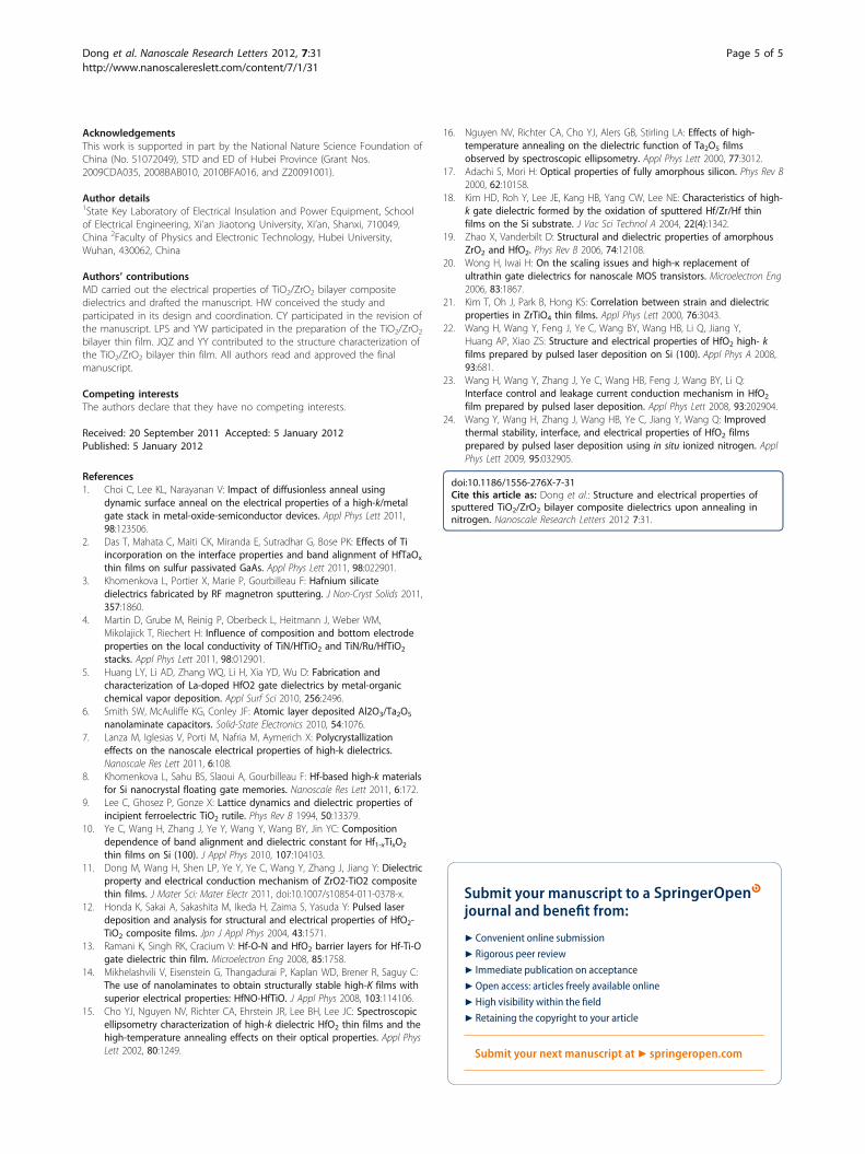
C-V characteristics of the MOS capacitor consisting ofPt/TiO2/ZrO2/p-Si was measured at high frequency (1MHz). Figure 4 shows the C-V curves for the ZrO2/TiO2 thin films. It can be seen that at 773 K annealedtemperature, the saturated capacitance is the highest.According to the saturated capacitance, we can get theeffective dielectric constant of the thin films. The dielec-tric constants of annealed composite thin films aremuch higher than those of the pure ZrO2 (about 20)[19], which indicate that TiO2 has been incorporated inthe ZrO2 film and improved the overall k value. Mean-while, the dielectric constants of the annealed samplesare higher than the as-deposited one, which is only 16.6and can be attributed to the series capacity of the two-layer structure [20]. At 773 K, the dielectric constant ofthe composite thin film is the highest and reaches themaximum of 46.1, while at 973 K, the dielectric constantdecreases to be 36.9. It can be concluded that thedielectric constants are affected by the annealing tem-perature. Normally, for a composite thin film, the dielec-tric constant is mainly dependent on the component ofthe film and the microstructure including the crystallineproperty, interface, surface roughness, and variousvacancies and defects in the film, etc. [21-24]. At 773 K,based on the above analyses, the multilayer film fullymixed, has good interfacial property, has the smallestsurface roughness, and has an amorphous structure,which results in the highest dielectric constant. Therelatively small k of 33.0 at 573 K may result from themultilayer film that was only partly mixed although thefilm is amorphous. At 973 K, the decrease of dielectricconstant is possibly due to interfacial reaction at highannealing temperature. We also obtain the flat band
voltage [Vfb] from the high frequency C-V curves. Vfb
primarily depends on deficiencies in theTiO2/ZrO2 filmand the interface traps at the interface. The smallest Vfb
is -0.53 V for the 773 K annealed thin film, and for theas-deposited and 573 K and 973 K annealed samples,the values of Vfb are -1.01, -0.71, and -0.62, respectively.It can be inferred from the Vfb that annealing canreduce the deficiencies or traps in the composite TiO2/ZrO2 thin film and that the annealing temperature of773 K is the optimal temperature.Figure 5 shows the density-voltage [J-V] characteristics
of all the samples with gate electron injection (negativeVg). As shown in Figure 5, all the annealed sampleshave lower leakage current density than the as-depositedone for the reason that annealing makes the film denserand reduces defects in the film. For the 773 K annealedthin film, the leakage current density is about 3.35 × 10⁻⁵ A/cm2 at the applied voltage of -1 V, which is slightlyhigher than that of other high-k oxide materials. Thismay be caused by the interface layer as shown in Figure2 and the defects in the film.
ConclusionThe high-k dielectric TiO2/ZrO2 bilayer composite filmwas prepared on a Si substrate by radio frequency mag-netron sputtering and post annealing in N2 at varioustemperatures in the range of 573 K to 973 K. Thebilayer film fully mixed together to become a compositesingle layer and has good interfacial property afterannealing at 773 K. The largest property permittivity of46.1 and a low leakage current density of 3.35 × 10⁻⁵A/cm2 were achieved for the sample of Pt/TiO2/ZrO2/Si/Pt after annealing at 773 K.
Figure 4 High-frequency (1 MHz) capacitance-voltage curves forTiO2/ZrO2/Si thin films. The inverted triangle represents the as-deposited sample; square, the sample annealed at 573 K; circle, thesample annealed at 773 K; and triangle, the sample annealed at 973 K.
Figure 5 Current-voltage curves for TiO2/ZrO2/Si thin films. Theinverted triangle represents the as-deposited sample; circle, thesample annealed at 573 K; square, the sample annealed at 773 K;and triangle, the sample annealed at 973 K.
Dong et al. Nanoscale Research Letters 2012, 7:31http://www.nanoscalereslett.com/content/7/1/31
Page 4 of 5
AcknowledgementsThis work is supported in part by the National Nature Science Foundation ofChina (No. 51072049), STD and ED of Hubei Province (Grant Nos.2009CDA035, 2008BAB010, 2010BFA016, and Z20091001).
Author details1State Key Laboratory of Electrical Insulation and Power Equipment, Schoolof Electrical Engineering, Xi’an Jiaotong University, Xi’an, Shanxi, 710049,China 2Faculty of Physics and Electronic Technology, Hubei University,Wuhan, 430062, China
Authors’ contributionsMD carried out the electrical properties of TiO2/ZrO2 bilayer compositedielectrics and drafted the manuscript. HW conceived the study andparticipated in its design and coordination. CY participated in the revision ofthe manuscript. LPS and YW participated in the preparation of the TiO2/ZrO2bilayer thin film. JQZ and YY contributed to the structure characterization ofthe TiO2/ZrO2 bilayer thin film. All authors read and approved the finalmanuscript.
Competing interestsThe authors declare that they have no competing interests.
Received: 20 September 2011 Accepted: 5 January 2012Published: 5 January 2012
References1. Choi C, Lee KL, Narayanan V: Impact of diffusionless anneal using
dynamic surface anneal on the electrical properties of a high-k/metalgate stack in metal-oxide-semiconductor devices. Appl Phys Lett 2011,98:123506.
2. Das T, Mahata C, Maiti CK, Miranda E, Sutradhar G, Bose PK: Effects of Tiincorporation on the interface properties and band alignment of HfTaOx
thin films on sulfur passivated GaAs. Appl Phys Lett 2011, 98:022901.3. Khomenkova L, Portier X, Marie P, Gourbilleau F: Hafnium silicate
dielectrics fabricated by RF magnetron sputtering. J Non-Cryst Solids 2011,357:1860.
4. Martin D, Grube M, Reinig P, Oberbeck L, Heitmann J, Weber WM,Mikolajick T, Riechert H: Influence of composition and bottom electrodeproperties on the local conductivity of TiN/HfTiO2 and TiN/Ru/HfTiO2
stacks. Appl Phys Lett 2011, 98:012901.5. Huang LY, Li AD, Zhang WQ, Li H, Xia YD, Wu D: Fabrication and
characterization of La-doped HfO2 gate dielectrics by metal-organicchemical vapor deposition. Appl Surf Sci 2010, 256:2496.
6. Smith SW, McAuliffe KG, Conley JF: Atomic layer deposited Al2O3/Ta2O5
nanolaminate capacitors. Solid-State Electronics 2010, 54:1076.7. Lanza M, Iglesias V, Porti M, Nafria M, Aymerich X: Polycrystallization
effects on the nanoscale electrical properties of high-k dielectrics.Nanoscale Res Lett 2011, 6:108.
8. Khomenkova L, Sahu BS, Slaoui A, Gourbilleau F: Hf-based high-k materialsfor Si nanocrystal floating gate memories. Nanoscale Res Lett 2011, 6:172.
9. Lee C, Ghosez P, Gonze X: Lattice dynamics and dielectric properties ofincipient ferroelectric TiO2 rutile. Phys Rev B 1994, 50:13379.
10. Ye C, Wang H, Zhang J, Ye Y, Wang Y, Wang BY, Jin YC: Compositiondependence of band alignment and dielectric constant for Hf1-xTixO2
thin films on Si (100). J Appl Phys 2010, 107:104103.11. Dong M, Wang H, Shen LP, Ye Y, Ye C, Wang Y, Zhang J, Jiang Y: Dielectric
property and electrical conduction mechanism of ZrO2-TiO2 compositethin films. J Mater Sci: Mater Electr 2011, doi:10.1007/s10854-011-0378-x.
12. Honda K, Sakai A, Sakashita M, Ikeda H, Zaima S, Yasuda Y: Pulsed laserdeposition and analysis for structural and electrical properties of HfO2-TiO2 composite films. Jpn J Appl Phys 2004, 43:1571.
13. Ramani K, Singh RK, Cracium V: Hf-O-N and HfO2 barrier layers for Hf-Ti-Ogate dielectric thin film. Microelectron Eng 2008, 85:1758.
14. Mikhelashvili V, Eisenstein G, Thangadurai P, Kaplan WD, Brener R, Saguy C:The use of nanolaminates to obtain structurally stable high-K films withsuperior electrical properties: HfNO-HfTiO. J Appl Phys 2008, 103:114106.
15. Cho YJ, Nguyen NV, Richter CA, Ehrstein JR, Lee BH, Lee JC: Spectroscopicellipsometry characterization of high-k dielectric HfO2 thin films and thehigh-temperature annealing effects on their optical properties. Appl PhysLett 2002, 80:1249.
16. Nguyen NV, Richter CA, Cho YJ, Alers GB, Stirling LA: Effects of high-temperature annealing on the dielectric function of Ta2O5 filmsobserved by spectroscopic ellipsometry. Appl Phys Lett 2000, 77:3012.
17. Adachi S, Mori H: Optical properties of fully amorphous silicon. Phys Rev B2000, 62:10158.
18. Kim HD, Roh Y, Lee JE, Kang HB, Yang CW, Lee NE: Characteristics of high-k gate dielectric formed by the oxidation of sputtered Hf/Zr/Hf thinfilms on the Si substrate. J Vac Sci Technol A 2004, 22(4):1342.
19. Zhao X, Vanderbilt D: Structural and dielectric properties of amorphousZrO2 and HfO2. Phys Rev B 2006, 74:12108.
20. Wong H, Iwai H: On the scaling issues and high-κ replacement ofultrathin gate dielectrics for nanoscale MOS transistors. Microelectron Eng2006, 83:1867.
21. Kim T, Oh J, Park B, Hong KS: Correlation between strain and dielectricproperties in ZrTiO4 thin films. Appl Phys Lett 2000, 76:3043.
22. Wang H, Wang Y, Feng J, Ye C, Wang BY, Wang HB, Li Q, Jiang Y,Huang AP, Xiao ZS: Structure and electrical properties of HfO2 high- kfilms prepared by pulsed laser deposition on Si (100). Appl Phys A 2008,93:681.
23. Wang H, Wang Y, Zhang J, Ye C, Wang HB, Feng J, Wang BY, Li Q:Interface control and leakage current conduction mechanism in HfO2
film prepared by pulsed laser deposition. Appl Phys Lett 2008, 93:202904.24. Wang Y, Wang H, Zhang J, Wang HB, Ye C, Jiang Y, Wang Q: Improved
thermal stability, interface, and electrical properties of HfO2 filmsprepared by pulsed laser deposition using in situ ionized nitrogen. ApplPhys Lett 2009, 95:032905.
doi:10.1186/1556-276X-7-31Cite this article as: Dong et al.: Structure and electrical properties ofsputtered TiO2/ZrO2 bilayer composite dielectrics upon annealing innitrogen. Nanoscale Research Letters 2012 7:31.
Submit your manuscript to a journal and benefi t from:
7 Convenient online submission
7 Rigorous peer review
7 Immediate publication on acceptance
7 Open access: articles freely available online
7 High visibility within the fi eld
7 Retaining the copyright to your article
Submit your next manuscript at 7 springeropen.com
Dong et al. Nanoscale Research Letters 2012, 7:31http://www.nanoscalereslett.com/content/7/1/31
Page 5 of 5