Embed Size (px)
Citation preview
Linköping Studies in Science and Technology Dissertation No. 1103
Studies of Materials and Interfaces
for Organic Electronics
Slawomir Braun
Department of Physics, Chemistry and Biology
Linköping University, SE-581 83 Linköping, Sweden

ISSN: 0345-7524
ISBN: 978-91-85831-94-4
Printed by UniTryck, Linköping, Sweden, 2007
Abstract
Organic electronics is a rapidly evolving field with vast number of applications
having high potential for commercial success. Although a great progress has been made,
many organic electronic applications: organic light-emitting diodes (OLEDs), organic
field-effect transistors (OFETs), organic solar cells, etc; still require further optimization
to fulfill the requirements for successful commercialization. For many applications,
available at this time organic materials do not provide satisfactory performance and
stability, which hinders the possibility of a large-scale production. Therefore, the key
ingredient needed for a successful improvement in performance and stability of organic
electronic devices is in-depth knowledge of physical and chemical properties of
molecular and polymeric materials. Since many applications encompass several thin
film layers made of organics, and often also inorganic materials, the understanding of
both organic-organic and hybrid interfaces is yet another important issue necessary for
the successful development of organic electronics.
The research presented in this thesis is based mainly on photoelectron
spectroscopy, which is an experimental technique especially suited to study both
surfaces and interfaces of materials. In the thesis, the properties of one of the most
successful polymeric materials, poly(3,4-ethylenedioxythiophene), often abbreviated as
PEDOT, have been extensively studied. The research was done in close cooperation
with an industrial partner – AGFA Gevaert, Belgium. The study was focused on the
exploration of the intrinsic properties of the material, such as stability, morphology and
conductivity. In addition, however, a possibility of alternation of these properties was
also explored. This thesis reports also about investigations of the properties of various
organic-organic and hybrid interfaces. The energy level alignment at such interfaces
plays important role in charge injection and performance of the thin film organic-based
devices. The conditions for different energy level alignment regimes at the various
interfaces have been studied. The studies on interfaces were performed in close
collaboration with the R&D division of DuPont Corporation, USA. This work led to the
significant advances in understanding of the interface energetics and properties of
industry-relevant organic materials, as represented not only by published scientific
papers, but also patent applications.


Sammanfattning
Organisk elektronik är ett snabbt växande område med många produkter med stora
möjligheter för kommersiell framgång. Trots stora framsteg krävs fortsatt optimering
för att uppnå de krav som finns för en framgångsrik kommersiallisering. För många
tillämpningar t.ex. organiska lysdioder, organiska fälteffekttransistor, organiska sol-
celler, osv uppvisar de material som finns tillgängliga idag varken tillräcklig prestanda
eller stabilitet, vilket förhindrar möjligheterna för storskalig produktion. Fördjupad
kunskap om fysiska och kemiska egenskaper av de molekulära och polymera materialen
är därför av stor vikt för att förbättra både prestanda och stabilitet inom organiska
elektronik. Eftesom många applikationer omfattar flera tunna lager av både organiska
och inorganiska material så är förståelsen av gränsnitten både mellan de organiska
materialen och mellan organiska och inorganiska material ett område där kunskap är av
stor vikt för framgångsrik utveckling av organisk elektronik.
Forskningen som presenteras i denna avhandling baseras till stor del på
fotoelektronspektroskopi, som är en teknik som särskilt lämpar sig för studier av både
ytor och gränssnitt mellan material. I den här avhandlingen har egenskaperna hos ett av
de mest framgångsrika polymera materialen, poly(3,4-ethylenedioxythiophene),
vanligtvis förkortat som PEDOT, blivit utförligt undersökta. Arbetet utfördes i nära
samarbete med en industriell partner – AGFA Gevaert, Belgien. Studien fokuserades på
att undersöka materialets inre egenskaper såsom stabilitet, morfologi samt
ledningsförmåga. Dessutom studerades möjligheterna till förändring av dessa
egenskaper. Avhandlingen innehåller också studier av gränssnitt mellan olika organiska
material samt gränssnitt mellan organiska och inorganiska material. Upplinjeringen av
elektronernas energinivåer vid sådana gränssnitt spelar en viktig roll vid
laddningsinjektion och prestanda hos de organiska komponenterna. Vilkoren för olika
fall av upplinjering av energinivåer har studerats hos ett antal olika gränssnitt. Studierna
av dessa gränssnitt har skett i nära samarbete med forskningsavdelningen på DuPont
Corporation, USA. Arbete ledde till stora framsteg i förståelsen för de
energiförhållanden som råder vid gränssnitten samt för de egenskaper hos organiska
material som är relevanta för industrin, vilket framgår inte bara av de publiserade
vetenskapliga artiklarna utan även av patent ansökningarna.

Preface
This thesis includes some of the research results that I have achieved
in the Surface Physics and Chemistry group at the Department of Physics, Biology and
Chemistry, Linköping University, Sweden.
The large part of the thesis is based on the projects which were carried in close
cooperation with industrial partners: Agfa-Gevaert N.V. (Mortsel, Belgium) and E. I.
DuPont de Nemours and Co., Inc., Dupont Displays, (research stations in Santa Barbara,
CA and Wilmington, DE, USA).
The projects can be divided in three parts: First – DOTCON project, mainly
focused on the study related to the properties of polymer blend: PEDOT-PSS, and was
carried out in close cooperation with AGFA Gevaert. The results from this project are
included in papers I and II in this thesis. The second project involved study on the other
PEDOT-related materials in a collaboration with Dupont Displays’ research station in
Santa Barbara. The materials studied are used in buffer layers in prototype polymer
light-emitting diodes PLEDs. The third project was focused on the issues related to the
energy level alignment at the interfaces relevant for organic light-emitting diodes
(OLEDs). Some of the results obtained are summarized in paper III. The topic of
interfacial energetics is further discussed in paper IV and paper V.


Acknowledgments
I would like to express my sincere thanks to:
� My supervisor Professor William R. Salaneck, for giving me opportunity to
work in the field of organic electronics, for his help and support expressed in
many ways, countless real-life stories, and most of all for his always positive
attitude.
� Dr. Xavier Crispin for help and discussions during DOTCON project.
� Dr. Ying Wang from Dupont Displays.
� All the members of Surface Physics and Chemistry group (present and former)
for help, the nice atmosphere and the conversations during coffee breaks.
� E. I. DuPont de Nemours and Co., Inc., USA, for financial support.
� My mother, father and sister: for everything they have done for me.
� My mother, father and sister – in law, for all the help and always warm welcome
in Poland and Germany.
� Friends that I have met in Linköping.
And last but definitely not least the great thanks to my dear wife Dagmara.


Papers included in the thesis:
• Light Induced Damage in Poly(3,4-ethylenedioxythiophene) and its Derivatives Studied by Photoelectron Spectroscopy
S. Marciniak*, X. Crispin, K. Uvdal, M. Trzcinski, J. Birgerson, L. Groenendaal, F. Louwet, and W. R. Salaneck
Synthetic Metals 141 (2004) 67-73
Author’s contribution:
Most of the experimental work and all of the data analysis. Wrote the first draft and responsible for the iterative process to the final version.
• Conductivity, Morphology, Interfacial Chemistry, and Stability of Poly(3,4- ethylene dioxythiophene)–Poly(styrene sulfonate): A Photoelectron Spectroscopy Study
X. Crispin, S. Marciniak*,
W. Osikowicz,
G. Zotti,
A. W. Denier Van Der Gon,
F. Louwet, M. Fahlman, L. Groenendaal,
F. De Schryver,
W. R. Salaneck
Journal of Polymer Science: Part B: Polymer Physics, 41(2003) 2561-2583
Author’s contribution:
Most of the experimental work and data analysis concerning: secondary doping, interfacial chemistry and light-induced degradation of PEDOT-C14, PEDOT-PSS and PSS. Took part in the process of writing.
• Energy level alignment regimes at hybrid organic–organic and inorganic–organic interfaces
S. Braun, W. Osikowicz, Y. Wang and W. R. Salaneck
Organic Electronics 8 (2007) 14-20
Author’s contribution:
All the experimental work and data analysis. Wrote the first draft and responsible for the iterative process to the final version.
*Name before marriage

• Fermi level pinning at interfaces with tetrafluorotetracyano-quinodimethane (F4-TCNQ): The role of integer charge transfer states.
S. Braun and W. R. Salaneck
Chemical Physics Letters 438 (2007) 259
Author’s contribution:
All the experimental work, theoretical work and data analysis. Wrote the first draft and responsible for the iterative process to the final version.
• Energy level alignment of organic interfaces under reversal of deposition sequence – the role of Fermi level pinning
S. Braun, M. P. de Jong, and W. R. Salaneck
submitted
Author’s contribution:
All the experimental work and data analysis. Wrote the first draft and responsible for the iterative process to the final version.

Related papers, not included in the thesis:
• Y. Wang1, W. R. Salaneck2, S. Braun2 US patent application No. 11/475407 - “Hole injection electrode” 1 E. I. DuPont de Nemours and Co., Inc., Dupont Displays, P.O. Box 80356, Experimental Station, Wilmington, Delaware 19880-0356 U.S.A. 2 Linköping University, Linköping, Sweden.
• Che-H-Hsu1, S. Marciniak*2, M. Fahlman2, W. R. Salaneck2 International patent application - WO/2005/090434 - “Water dispersible polydioxythiophenes with polymeric acid colloids and a water-miscible organic liquid”
1 E. I. DuPont de Nemours and Co., Inc., Dupont Displays, Santa Barbara, CA 93117, U.S.A. 2 Linköping University, Linköping, Sweden.
• Ultraviolet light–ozone treatment of poly(3,4-ethylenedioxy-thiophene)-based
materials resulting in increased work functions. C. Tengstedt, A. Kanciurzewska, M. P. de Jong, S. Braun, W. R. Salaneck and M. Fahlman, Thin Solid Films, 515 (2006) 2085.
• Structure and mechanical properties of arc evaporated Ti-Al-O-N thin films. J. Sjölen, L. Karlsson, S. Braun, R. Murdey, A. Hörling and L. Hultman, Surf. Coat. Tech., 201 (2007) 6392.
• Energetics at Au top and bottom contacts on conjugated polymers.
W. Osikowicz, M. P. de Jong, S. Braun, C. Tengstedt, M. Fahlman and W. R. Salaneck, Appl. Phys. Lett. 88 (2006) 193504.
• Enhancement of Iridium-based organic light-emitting diodes by spatial doping of the hole transport layer. Y. Wang, W. Gao, S. Braun, W. R. Salaneck, F. Amy, C. Chan and A. Kahn, Appl. Phys. Lett. 87 (2005) 193501.
• Poly(3,4-ethylene dioxythiophen)- and Polyaniline- Poly(perfluoroethylene-sulfonic acid) a photoelectron spectroscopy study. C. Tengstedt, S. Braun, W. R. Salaneck and M. Fahlman, submitted
• Solution-processed, highly-oriented nanocolumns of functionalized porphyrins with extended electronic states. R. Friedlein, F. von Kieseritzky, S.Braun, Ch. Linde, W. Osikowicz, J. Hellberg, W. R. Salaneck, Chem. Commun. 15 (2005) 1974.
• Surface-induced vertical alignment of self-assembled supramolecular columns of large polycyclic aromatic hydrocarbons and porphyrins. R. Friedlein, X. Crispin, W. Osikowicz, S. Braun, M. P. de Jong, C. D. Simpson, M. D. Watson, F. von Kieseritzky, P. Samorí, S. K. M. Jönsson, M. Fahlman, F. Jäckel, J. P. Rabe, J. Hellberg, K. Müllen, W. R. Salaneck, Synth. Met. 147 (2004) 79.
• Core excitations of napthalene: Vibrational structure versus chemiacal shifts. Minkov, F. Gel’mukhanov, R. Friedlein, W. Osikowicz, C. Suess, G. Örhwall, S. L. Sorensen, S. Braun, R. Murday, W. R. Salaneck, H. Ågren, J. Chem. Phys. 121 (2004) 5733.
• Stability of indium tin oxide/polymer interfaces. Crispin, X. Crispin, A.; de Jong, M.P.; Marciniak,* S.; Osikowicz, W.; Jonsson, S.; Fahlman, M.; Kugler, T.; van Ijzendoorn, L.J.; de Voigt, M.J.A.; Salaneck, W.R. Mater. Res. Soc. Symposium Proceedings, Vol.747 (2003) 315.
• Electronic structure of highly ordered films of self-assembled graphitic nanocolumns. R. Friedlein, X Crispin, C. D. Simpson, M.D. Warson, F. Jäckel, W. Osikowicz, S. Marciniak*, M. P. de Jong, P. Samori, S. K. M. Jönsson, M. Fahlman, K. Mullen, J. P. Rabe, and W. R. Salaneck. Phys. Rev. B 68 (2003) 195414.
*Name before marriage
1
Content
1. Introduction 3
2. Organic materials 7
2.1 Background 7 2.2 The electronic structure of some conjugated polymers 10 2.3 Charge carriers: solitons, polarons, bipolarons 12 2.4 Doping of organic materials 14 2.5 Poly(3,4-ethylenedioxythiophene) – PEDOT 16
3. Interfaces in organic electronics 19
3.1 An example of organic electronic device: organic light-emitting diode (OLED) 20
3.2 Operational principles of OLEDs 21 3.3 The role of interfaces for charge injection 24
4. Quantum chemical calculations 27
5. Experimental technique 29
5.1 Background information 30 5.2 The theory of photoelectron emission 33 5.3 XPS – core level spectroscopy 35 5.4 UPS – spectroscopy of valence levels 36 5.5 The reference level 38
6. Experimental Equipment 41
7. References 43
Paper I 51
Paper II 69
Paper III 111
Paper IV 127
Paper V 139

2

3
11
Introduction
Organic electronics is now a rapidly evolving research field with vast number of
applications having high potential for commercial success. Research in this field is
conducted on a largely multidisciplinary level, involving: theoretical physics and
chemistry, synthetic chemistry, various material and device characterization methods,
device engineering. In order to fulfill the demand for the expertise necessary to
appropriately address the organic electronics-related scientific topics, the research
projects are often conducted in co-operations between various research groups. Since
organic electronics has a potential to provide substantial revenues in the near future,
electronic and chemical industries also show increasing interest in this field. As an
outcome of this interest a significant research effort is also undertaken by industrial
research and development (R&D) laboratories. It is worth noting that a significant part
of this thesis is based on the research conducted with close collaboration with the
industrial partners.
For the development of new organic electronic applications and improvement of
performance of the already existing prototype devices, materials with desired properties
play an instrumental role. They are the key ingredients, which provide competing
functionalities (e.g. flexibility, lightweight) to the electronic devices. One of the most
advantageous features, associated however mostly with soluble organic materials, is
their good processing ability. The various organic-based devices can be made by

4
printing methods, e.g. inkjet, roll-to-roll, which simplifies and speeds up the production
process. Consequently, it also greatly lowers the manufacturing costs, which are often
regarded as the deciding factors for successful commercialization of the devices.
Some of the developed organic materials already exhibit properties enabling
their use in the electronic devices. Though for many applications, available at this time
materials, do not provide satisfactory device performance and operational stability.
Nowadays these shortcomings definitely hinder the progress in commercialization of
organic-based electronic devices. For the sustainable development of organic electronics
in-depth knowledge and understanding of physical and chemical properties of organic
materials is necessary. One of the biggest drawbacks of organics is its tendency for
alternation of properties not only during operation of devices but even under ambient
conditions (often referred to as ageing). This in-turn constitutes a significant problem
that limits both shelf and operational lifetime of the devices. In this thesis, papers: I and
II contain research results related to the stability of organic materials. Since many
organic electronic applications encompass several thin film layers made of organics, and
often also inorganic materials, the understanding of interfaces is another important issue
for the development of organic electronics. The energy level alignment at various
organic-organic and hybrid interfaces has been studied in papers: III, IV and V.
Research presented in this thesis is based predominantly on photoelectron
spectroscopy. This material characterization technique is a very fruitful method for
studying physical and chemical properties of organic materials. The possibility of high-
resolution x-ray photoelectron spectroscopy (XPS) and ultraviolet photoelectron
spectroscopy (UPS) measurements allow for studying electronic and chemical
properties of the materials.1-5 Since photoelectron spectroscopy is a surface sensitive
technique, physical and chemical interactions at surfaces and interfaces can be studied
in details. Ultraviolet photoelectron spectroscopy is also very useful for studies of
interfaces since it enables direct probing of the occupied valence electronic levels as
well as vacuum level shifts upon forming the interface.
The thesis comprises of an introductory part, which is expected to provide a
short description of the concepts involved in the presented papers. In the chapter 2 the
basic information concerning conjugated organic materials is given. Since the first two
papers included in the thesis, relate to the properties of the conjugated polymer

5
poly(3,4-ethylenedioxythiophene) (PEDOT), some background information related to
this polymer is included in the chapter 2. In chapter 3, a general description of interfaces
and their role for operational conditions in organic electronic devices, is presented. The
next chapter contains short description of quantum chemical calculations of electronic
structures. Some theoretical aspects of photoelectron spectroscopy are included in
chapter 5. Chapter 6 presents the equipment on which experimental work has been
performed. In the next part of the thesis the scientific publications are presented.

6
7
22
Organic materials
2.1 Background
The discovery of the dramatic increase in electrical conductivity, upon doping
of semiconducting polymers, established the foundation to the field of organic
electronics.6,7 Since then, the doped conjugated polymers, as well as molecules, have
been extensively studied in the context of their possible application in organic electronic
devices. Organic materials found they way in many applications like: light-emitting
diodes,27 transistors,15 photovoltaic devices,8 photo-detectors,9 polymer-based
memories,10,11 chemical vapor sensors,12 etc. Hence, to a large extend the prospects for a
new organic electronic industry has been the driving force for the research and
engineering efforts concerning this class of materials for already many years. It should
be realized that organic materials provide a combination of properties that are not found
for inorganics. This combination includes lightweight, flexibility, relatively easy
processing as well as controllable in a wide range electrical conductivity. Though there
exist significant drawbacks that must be overcome in order to make devices that fulfill
commercial requirements. The development of new molecules and polymers has
enabled continuous progress of the knowledge in the field. The number of possible
applications has grown as materials with desired properties became available.
8
Organic materials are composed mainly of carbon atoms. Other low atomic number
atoms, like: oxygen, sulfur, are also common building elements. The electronic
configuration of carbon atom allows it to form different hybridized orbitals, namely sp,
sp2 and sp3, as the chemical bonding configuration. The electronic configuration of
carbon atom consists of 2 electrons in core 1s level denoted as 1s2 and 4 valence
electrons residing in 2s and 2p levels, which can be denoted as 2s2 and 2p2, respectively.
In order to explain electronic configuration in different compounds involving carbon,
the concept of hybridized orbitals is used. Hybridized orbitals are assumed to be
mixtures of atomic orbitals. The wave functions of the s and p atomic orbitals combine
to form a new set of equivalent hybrid orbitals. New orbitals are linear combinations of
atomic orbitals and the reason they form is to minimize the total energy of the formed
compound.13 When one s orbital mixes with three p orbitals it yields four sp3 type
hybrid orbitals. Each of them consists of two lobes of different size. Four larger lobes
are oriented towards the corners of a tetrahedron at angles of 109.5º. When carbon
atoms are bonded in such a scheme each of them has four neighbors. This configuration
can be found in diamond. Another type of hybridization is the one that involves only
one s and two p atomic orbitals. The three hybrids are span in the plane and are oriented
at angles of 120º to one another and contain one electron each. The remaining electron
resides in unhybridized p orbital oriented perpendicular to the plane of sp2 orbitals. This
type of hybridization will be discussed in more details in the context of conjugated
polymers. Here, for completeness the remaining sp configuration will be presented. In
that case only one s and one p electrons form hybrid orbital. The remaining two p
electrons are unhybridized and reside in orbitals oriented at 90º to the sp hybrids. Such
hybridization scheme accounts for linear geometries.
When two atoms are bond through hybridized orbitals, two different types of
bond exist, depending on their alignment with respect to the bonding direction. Sigma
bonds, denoted as σ, are symmetrical about the axis joining the two nuclei. This type of
bond allows for rotation of atoms along the bonding direction. Most often such rotation
is prevented by existence of π bonding. This bonding is constructed from electrons in
unhybridized p orbitals and geometrically is perpendicular to the axis joining two
nuclei. Hence, when two carbon atoms are bonded through σ and π bonds, the later
prevent rotation of these two atoms. These two types of bonds differ significantly by
means of their strength. Since the spatial overlap of orbitals is larger for σ type of
bonding than π type, the later is significantly weaker. This invokes consequences for the
9
energy associated with σ or π electronic levels in a molecule (or bands in a polymer).
The general picture in both cases is such that σ states are always lower in energy than π
states (and vice versa for the occupied states).
The existence of a single, double or triple bonds corresponds directly to the type of
hybridization occurring when a molecule or polymer is formed. Another consequence of
different hybridization schemes is the geometry of a compound.
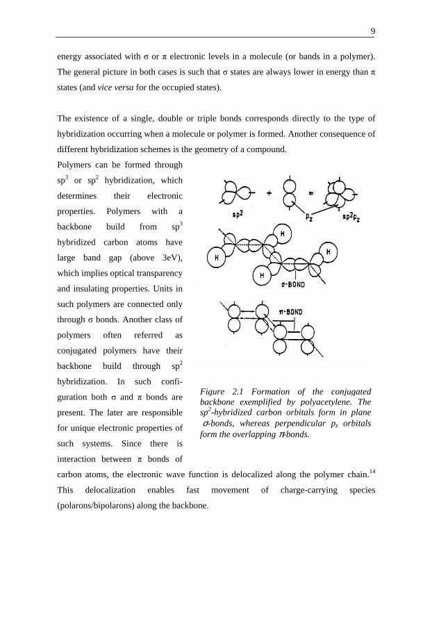
Polymers can be formed through
sp3 or sp2 hybridization, which
determines their electronic
properties. Polymers with a
backbone build from sp3
hybridized carbon atoms have
large band gap (above 3eV),
which implies optical transparency
and insulating properties. Units in
such polymers are connected only
through σ bonds. Another class of
polymers often referred as
conjugated polymers have their
backbone build through sp2
hybridization. In such confi-
guration both σ and π bonds are
present. The later are responsible
for unique electronic properties of
such systems. Since there is
interaction between π bonds of
carbon atoms, the electronic wave function is delocalized along the polymer chain.14
This delocalization enables fast movement of charge-carrying species
(polarons/bipolarons) along the backbone.
Figure 2.1 Formation of the conjugated backbone exemplified by polyacetylene. The sp2-hybridized carbon orbitals form in plane σ-bonds, whereas perpendicular pz orbitals form the overlapping π-bonds.
10
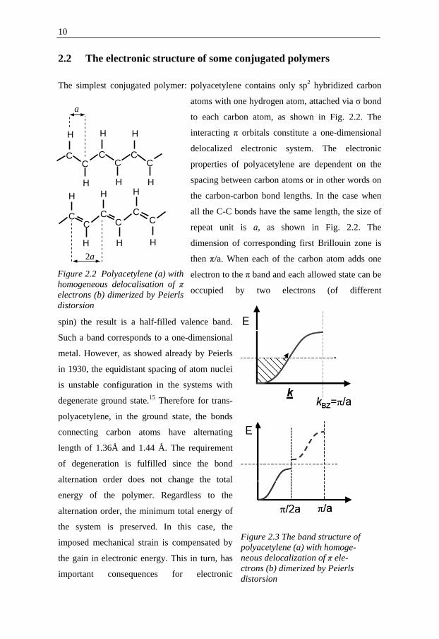
2.2 The electronic structure of some conjugated polymers
The simplest conjugated polymer: polyacetylene contains only sp2 hybridized carbon
atoms with one hydrogen atom, attached via σ bond
to each carbon atom, as shown in Fig. 2.2. The
interacting π orbitals constitute a one-dimensional
delocalized electronic system. The electronic
properties of polyacetylene are dependent on the
spacing between carbon atoms or in other words on
the carbon-carbon bond lengths. In the case when
all the C-C bonds have the same length, the size of
repeat unit is a, as shown in Fig. 2.2. The
dimension of corresponding first Brillouin zone is
then π/a. When each of the carbon atom adds one
electron to the π band and each allowed state can be
occupied by two electrons (of different
spin) the result is a half-filled valence band.
Such a band corresponds to a one-dimensional
metal. However, as showed already by Peierls
in 1930, the equidistant spacing of atom nuclei
is unstable configuration in the systems with
degenerate ground state.15 Therefore for trans-
polyacetylene, in the ground state, the bonds
connecting carbon atoms have alternating
length of 1.36Å and 1.44 Å. The requirement
of degeneration is fulfilled since the bond
alternation order does not change the total
energy of the polymer. Regardless to the
alternation order, the minimum total energy of
the system is preserved. In this case, the
imposed mechanical strain is compensated by
the gain in electronic energy. This in turn, has
important consequences for electronic
Figure 2.3 The band structure of polyacetylene (a) with homoge-neous delocalization of π ele-ctrons (b) dimerized by Peierls distorsion
C
H
C
H
C
H
C
H
C
H
C
H
Figure 2.2 Polyacetylene (a) with homogeneous delocalisation of π electrons (b) dimerized by Peierls distorsion
C
H
C
H
C
H
C
H
C
H
C
H
a
2a
11
properties of the polymer. Even though the length of the bonds differs only by 0.08 Å,
the electronic properties are changed dramatically.16 Due to the bond alternation, the
repeat unit along the dimerized chain doubles the size. Since the dimension of the
Brillouin zone is inverse distance of the unit cell, the first Brillouin zone moves into the
position of π/2a (Fig. 2.3). Consequently, the zone edge of the dimerized chain meets
the band structure just at the Fermi energy. The energetic gap opens up at the Fermi
level, which is manifested by semiconducting properties of trans polyacetylene.17,18
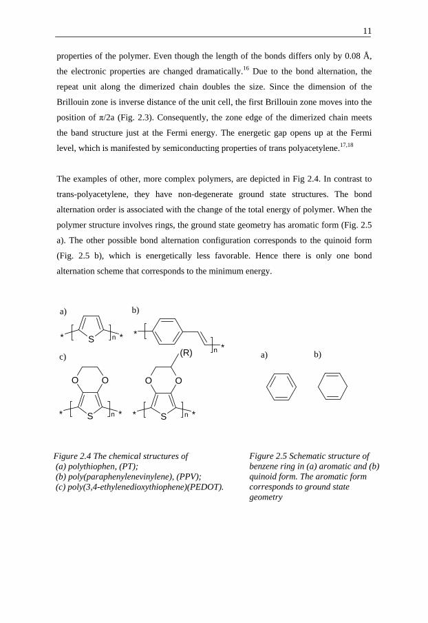
The examples of other, more complex polymers, are depicted in Fig 2.4. In contrast to
trans-polyacetylene, they have non-degenerate ground state structures. The bond
alternation order is associated with the change of the total energy of polymer. When the
polymer structure involves rings, the ground state geometry has aromatic form (Fig. 2.5
a). The other possible bond alternation configuration corresponds to the quinoid form
(Fig. 2.5 b), which is energetically less favorable. Hence there is only one bond
alternation scheme that corresponds to the minimum energy.
Figure 2.5 Schematic structure of benzene ring in (a) aromatic and (b) quinoid form. The aromatic form corresponds to ground state geometry
S
OO
* *n
S* *n
S
OO
* *n
*
*
n
(R)
a) b)
c) a) b)
Figure 2.4 The chemical structures of (a) polythiophen, (PT); (b) poly(paraphenylenevinylene), (PPV); (c) poly(3,4-ethylenedioxythiophene)(PEDOT).

12
2.3 Charge carriers: solitons, polarons, bipolarons
The bond alternation scheme in any conjugated polymer can be locally (several
units) distorted. Such distortion perturbs the electronic structure so that new available
states are created. These states appear in the previously forbidden energy gap, therefore
their presence changes properties of the material. The short description of possible new
states will be now presented.
As mentioned in the previous paragraph, polymers may have degenerate or non-
degenerate ground state geometry. In the first case, the local bond alternation disruption
may be introduced and leads to a new state called soliton. Interestingly the new state has
no charge but has a spin. The charge can be added or withdrawn from such a state,
which leads to positively or negatively, charged solitons.
Since the neutral soliton has a spin, addition or extraction of an electron cancels the net
spin. In the case of negatively charged solitons the resulting electronic structure of
polymer includes half-filled states (bands) at Fermi level. Therefore presence of these
states invokes electrical conductivity increase of the polymer. The soliton states may be
induced by absorption of light, or by "doping", when charge-exchange process occurs
between the polymer chain and a dopant (e.g. atom, molecule). From the chemical point
of view such doped system can be viewed as salt.19
The majority of conjugated polymers have non-degenerate ground state.
Therefore, in such systems, formation of soliton would convert the polymer geometry to
a more quinoid like structure. This, in turn, would raise the total energy, since there is
S0
S+
S-
VB
CB
VB
CB
VB
CB
S0
S+
S-
Figure 2.6 Schematic representation of solitons in trans-acetylene.
13
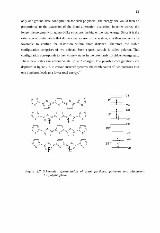
only one ground state configuration for such polymers. The energy rise would then be
proportional to the extension of the bond alternation distortion. In other words, the
longer the polymer with quinoid-like structure, the higher the total energy. Since it is the
extension of perturbation that defines energy rise of the system, it is then energetically
favorable to confine the distortion within short distance. Therefore the stable
configuration comprises of two defects. Such a quasi-particle is called polaron. This
configuration corresponds to the two new states in the previously forbidden energy gap.
These new states can accommodate up to 2 charges. The possible configurations are
depicted in figure 2.7. In certain material systems, the combination of two polarons into
one bipolaron leads to a lower total energy.20
Figure 2.7 Schematic representation of quasi particles: polarons and bipolarons for polythiophene.
VB
CB P+
VB
CB BP++
VB
CB P-
VB
CB BP--
S
S
S
SS
S
S
S
SS
S
S
S
SS
S
S
S
SS
14
2.4 Doping of organic materials
In the ground state, conjugated polymers are semiconductors with the band gap
mostly confined within 1-3.5eV range. However, as it was discussed in the previous
paragraph, the change in bond alternation scheme influences the electronic structure so
that new states (polarons or bipolaron) are created. In the presence of electric field,
these charge carriers can move along the polymer backbone since there is conjugation
of π orbitals. The distortion of bond alternation can be imposed by addition or extraction
of charge often called - doping. When the doping level is sufficiently high, the
electronic structure evolves to that of a metal.6 Consequently, the modification of the
physical properties (conductivity, optical response) of a doped material is observed.
There are various methods which allow for doping of organic materials:
• charge-transfer redox chemistry – chemical doping
• electrochemical doping
• photo-doping
• interfacial doping
The first type of doping involves oxidation (p-type doping), or reduction (n-type
doping) by interaction of polymer chain with atomic or molecular charge donors (or
acceptors). Upon interaction the new states are created in polymer chain while the
dopant maintains charge neutrality thus acting as counter ion. The chemical doping can
be maintained both on molecular or polymeric systems, and is rather efficient though
difficult to control. The later issue is strongly related to the fact that amount of dopant
introduced in the material often does not correspond to the achieved doping ratio.
Chemical doping was the mechanism involved in the discovery of conducting polymers.
Performed on trans-polyacetylene yielded metallic material with conductivity close to
that of copper.21
In electrochemical doping the polymer is reduced or oxidized by the redox
charge, provided by electrode. Results presented in paper I and II in this thesis involves
PEDOT samples prepared by this method. The role of electrolyte is to compensate the
electronic charge. Practically, doping at any level can be achieved by controlling the
15
voltage and time of the reaction. When the system is at electrochemical equilibrium, the
doping level is determined by voltage between the conducting polymer and the counter
electrode. For some materials this process can be reversed. Since doping is associated
with change of conductivity or sometimes other properties, this can be utilized in a
practical way. This property makes such materials promising for applications like
electrochromic windows,22,23 transistors, 24 etc.
So far, the types of doping discussed provide changes in a polymer that are
relatively stable in time. In these cases the induced electrical conductivity is permanent
as long as the charge carriers are not chemically compensated or removed by undoping.
In the case of photo-doping the induced effect can be transient and exists only until the
excitations decay back to the ground state. Similarly, the interfacial-doping rely on the
applied voltage. It is worth noting that the doping can be performed not only on
polymers but also on small molecules. The doping can be realized via charge exchange
with “guest” molecules or with atoms like Na or Li and leads to the new electrical
properties of a molecular layer.25-28 In paper IV, the doping with sodium atoms of
vacuum deposited molecular films of tetrafluoro-tetracyanoquinodimethane (F4-
TCNQ) was performed. The studies have revealed that the doping significantly alters
the electronic structure of the molecules. Moreover, it was shown that the observed
doped-induced changes are reminiscent of the interfacial states observed for a
submonolayer deposited on Aluminum oxide substrate.
There is also a certain type of doping that significantly increases conductivity of
polymeric films but is not associated with a process of charge exchange. Such a doping
is called: secondary doping and relates to the inclusion of an inert substance that
enhances conductivity of already (primarily) doped system. Such a substance, usually
organic solvent, introduces various changes to the polymeric system: changes in a chain
conformation, changes in the interaction strength between the polymer and counterions
or changes in morphology. The inclusion of a secondary dopant may also promote better
chain stacking which in turn enables better charge hopping between polymer chains.
Consequently, a better pathway for charges to travel in the polymeric film (via inter-
chain hopping) is available.
16
2.5 Poly(3,4-ethylenedioxythiophene) (PEDOT) – a conjugated polymer
Conjugated polymer - PEDOT has a unique combination of properties which
makes it extremely attractive for organic electronics applications.29 It is utilized in
organic-based optoelectronic devices: as a charge injecting layer in light-emitting
devices;30,31 as a component in electrochromic displays22 and even as electrodes in field-
effect transistors32 and photovoltaic cells.33
PEDOT is an intrinsically insoluble polymer, which can be chemically or
electrochemically doped (doping processes are discussed in paragraph 2.4). Doping
transforms PEDOT from an opaque insulator to a quasi-transparent material with high
electrical conductivity.34,35
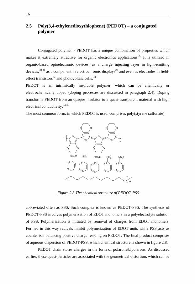
The most common form, in which PEDOT is used, comprises poly(styrene sulfonate)
abbreviated often as PSS. Such complex is known as PEDOT-PSS. The synthesis of
PEDOT-PSS involves polymerization of EDOT monomers in a polyelectrolyte solution
of PSS. Polymerization is initiated by removal of charges from EDOT monomers.
Formed in this way radicals inhibit polymerization of EDOT units while PSS acts as
counter ion balancing positive charge residing on PEDOT. The final product comprises
of aqueous dispersion of PEDOT-PSS, which chemical structure is shown in figure 2.8.
PEDOT chain stores charges in the form of polarons/bipolarons. As discussed
earlier, these quasi-particles are associated with the geometrical distortion, which can be
S
OO
S
OO
S
OO
*S
OO
*n
+
**
SO3SO3 SO3H SO3HSO3H - -
n
Figure 2.8 The chemical structure of PEDOT-PSS
17
delocalized over several monomer units. The charges are balanced by presence of SO3-
groups of PSS. Films formed from PEDOT-PSS dispersion have conductivity of about
0.01-0.05 [S/cm]. The substantial increase in conductivity of the films can be achieved
through the process called: secondary doping. (in paper II, a three orders of magnitude
increase of conductivity is reported as the effect of secondary doping). The mechanism
of the secondary doping is discussed in chapter 2.4.
The distinct property of PEDOT-PSS is its ability to form aqueous dispersion.
This is possible because of the long chains of polystyrene sulfonates. In the form of
dispersion this polymeric complex is ideal for making thin conducting films by spin
coating. This method of film preparation enables large-scale and low-cost production of
the devices.
PEDOT-PSS has also been used as a buffer layer in organic-light emitting
diodes (OLEDs) sandwiched between inorganic electrode indium tin oxide (ITO) and an
active layer of an electroluminescent polymer or a layer of evaporated small-molecules.
The presence of PEDOT-PSS smoothes rough surface of ITO and increases the work
function of the electrode. Interfacial chemistry between PEDOT-PSS and ITO is
important in the context of device operational stability and lifetime. This issue is of the
main focus in paper II. PEDOT-PSS films have intrinsically high work function of
about 5.2eV that facilitates good conditions for hole injection.26 Thanks to the recent
achievements in development of this material it is also possible to obtain PEDOT-based
films with different work functions.36 The exceptionally high work function (up to 6.1
eV), can be obtained from the other PEDOT-based system: PEDOT-PFESA [or
poly(3,4-ethylenedioxythiophene) poly(per- fluoroethylene sulfonic acid)]. The work
function of PEDOT-PFESA films can be tuned by exposure to UV radiation or by a
chemical modification of the dispersion. Both methods however, alter conductivity of
the films.37 A dispersion of PEDOT-PFESA has been used to prepare high work
function films in order to study energy-level alignment with various molecular materials
(see papers: III, IV and V).

18
19
33
Interfaces in organic electronics
In this chapter the motivation for studying the interfaces relevant for organic
electronics is described. In the further part, the example of an organic device: organic
light-emitting diode (OLED) is given. Finally the role of interfaces in organic-based
devices like OLEDs is discussed.
Since applications like organic light-emitting diodes (OLED), organic field-
effect transistors (OFET) or photovoltaic cells, encompass several thin film layers, the
understanding of interfaces is a central issue for the further development of these
devices. The particularly important seems to be the electronic level alignment at the
interfaces of various organic materials. The importance of this topic is related to the fact
that the interfacial energetics sets the condition for the injection of charges in a device,
which has a profound influence on the device operational characteristics, i.e. current-
voltage characteristic. Interfaces have been studied by various research groups and a
great progress in their understanding has been made.5,26,38-60 However, despite all these
efforts, the energetics of organic-organic and hybrid interfaces is still not completely
understood. The attempt of finding a model that would be capable to predict the energy
level alignment of broad range of interfaces has been made by Vázquez and co-workers.
A model of energy level alignment at the “atomically clean” metal–organic and
organic–organic interfaces was proposed, where the interfacial electronic structure was
interpreted in terms of induced density of interface states (IDIS).61-63 In the recent
20
studies, however, it was shown that various type of interfaces do not comply with this
model.64-66
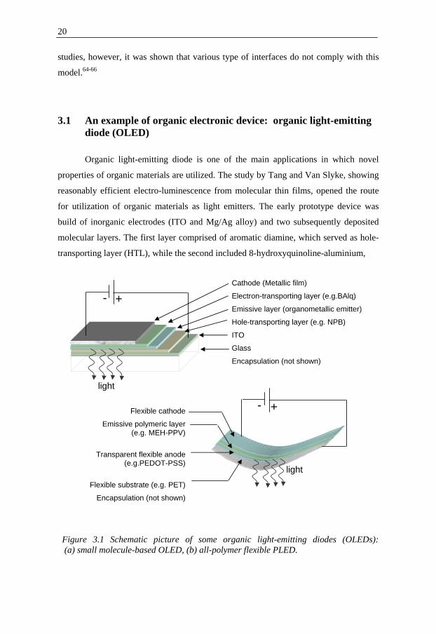
3.1 An example of organic electronic device: organic light-emitting diode (OLED)
Organic light-emitting diode is one of the main applications in which novel
properties of organic materials are utilized. The study by Tang and Van Slyke, showing
reasonably efficient electro-luminescence from molecular thin films, opened the route
for utilization of organic materials as light emitters. The early prototype device was
build of inorganic electrodes (ITO and Mg/Ag alloy) and two subsequently deposited
molecular layers. The first layer comprised of aromatic diamine, which served as hole-
transporting layer (HTL), while the second included 8-hydroxyquinoline-aluminium,
+ - Cathode (Metallic film)
Electron-transporting layer (e.g.BAlq)
Emissive layer (organometallic emitter)
Hole-transporting layer (e.g. NPB)
ITO
Glass
Encapsulation (not shown)
Flexible cathode
Emissive polymeric layer (e.g. MEH-PPV)
Transparent flexible anode (e.g.PEDOT-PSS)
Flexible substrate (e.g. PET)
Encapsulation (not shown)
light
light
+ -
Figure 3.1 Schematic picture of some organic light-emitting diodes (OLEDs): (a) small molecule-based OLED, (b) all-polymer flexible PLED.
21
which was the emissive layer.67,68 The discovery led to extensive research devoted to the
improvement of OLEDs operational conditions and performance.69 The simple structure
of the early OLEDs has gradually evolved to the multi-layered devices as shown in
figure 3.1.70,71 The incorporation of the HTL and electron-transporting layers (ETL)
provides balancing of charges entering the emissive layer.72
The possibility of using polymers as an electroluminescent material in a diode
has been reported by the group of Prof. R. H. Friend from University of Cambridge.
Electroluminescence from conjugated polymers was first reported in 1990, using
poly(p-phenylene vinylene), PPV, as the single semiconductor layer inserted between
metallic electrodes. PPV has an energy gap of about 2.5 eV, and produces yellow-green
luminescence.73 After this discovery many other polymers like polyfluorenes (PFO) and
polyspiro materials have been synthesized and utilized as emitters.74-76 Unlike small
molecules, polymers can be processed by wet chemistry methods like spin coating or
ink jet printing. The common configuration for polymer-based diodes is very similar to
those comprising small molecules. ITO is used as transparent anode,77-79 which allows
the light generated within the diode to leave the device. Then the layer of
electroluminescent polymer is deposited followed by deposition of top electrode. The
later is obtained by thermal evaporation of a low work function metal or a metallic
alloy.
The apparent advantage of polymer light-emitting diodes (PLEDs) is the
possibility of fast and cheap manufacturing. Some of the polymers are soluble in water
or organic solvents, which enables convenient preparation of thin layers by spin coating.
In contrast, organic layers in small molecule-based devices are prepared at least under
high vacuum conditions. Therefore the process is more expensive and time consuming
with respect to their polymer-based counter parts. Substitution of inorganic electrodes
into flexible and conducting polymer layers (e.g., PEDOT-PSS) gives opportunity for
all-polymer flexible devices.80 Such devices can be utilized in applications were
flexibility and large surface is desired.
22
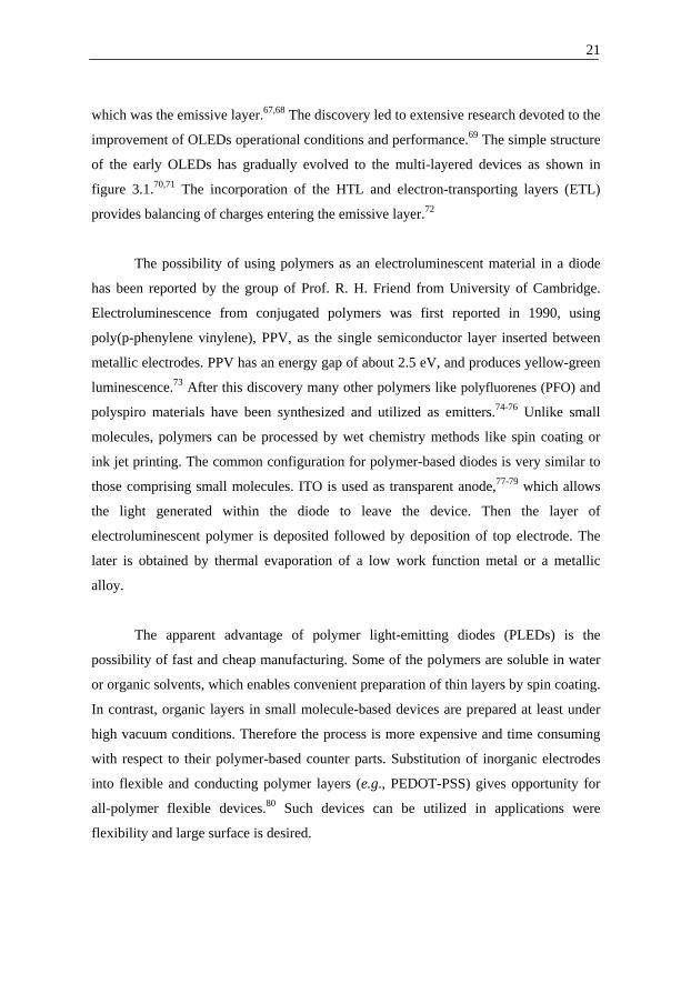
3.2 Operational principles of OLEDs
In OLED devices, light is produced through the process of electroluminescence.
In this process excitons (hole–electron pairs or oppositely charged pairs of polarons) are
formed within emissive layer. In order to form excitons positive and negative charges
must be injected into electroluminescent layer in the device. Charge supply is
maintained either directly by the electrodes or what is more often the case, through the
hole- and electron- transporting layers. The injected charges migrate and form excitons
via coulombic interaction. De-excitation occurs through recombination process, which
may be radiative or not, depending on spin configuration. In an emissive layer
comprising of entirely fluorescent material, according to spin statistics, only the
minority of states formed are singlets (25%) while the rest have triplet character. Since
only singlets may decay radiatively, the internal quantum efficiency of the
recombination process is dramatically reduced with respect to the total number of
created excitonic pairs. In small-molecules based OLEDs, significant increase in
efficiency was achieved by biasing singlet-triplet statistics. This can be done by using
so-called triplet emitters. In such molecules singlet and triplet states are mixed through
strong spin-orbit coupling induced by a heavy atom. Such molecules are referred as
organo-metallic molecules since they include atoms like Ir or Pt.81-83 The presence of
heavy atoms influences electronic properties of the molecules in such way that the
excited states are not entirely of singlet or triplet character. In organo-metallic
compounds the time scale for (forbidden) triplet de-excitation is much shorter that in
fluorescent dyes and leads to
emissive decay. Recently, research
effort is also focused on biasing
spin statistics in polymers. 84,85
The extraction of photons
produced is also important issue
since upon de-excitation, photons
propagate in every direction from
the recombination site. Therefore,
only some of them propagate in the
direction of a semi-transparent
electrode comprised of e.g. glass
EF
EvF
Emissive Layer
cathode HTL
ETL
vacuum level
EF
-
+
anode hv
Figure 3.2 Schematic picture of energy levels in an OLED.
23
and ITO, and escape from the device.
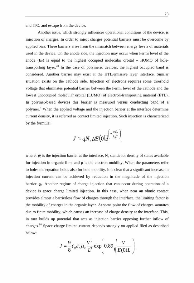
Another issue, which strongly influences operational conditions of the device, is
injection of charges. In order to inject charges potential barriers must be overcome by
applied bias. These barriers arise from the mismatch between energy levels of materials
used in the device. On the anode side, the injection may occur when Fermi level of the
anode (EF) is equal to the highest occupied molecular orbital – HOMO of hole-
transporting layer.38 In the case of polymeric devices, the highest occupied band is
considered. Another barrier may exist at the HTL/emissive layer interface. Similar
situation exists on the cathode side. Injection of electrons requires some threshold
voltage that eliminates potential barrier between the Fermi level of the cathode and the
lowest unoccupied molecular orbital (LUMO) of electron-transporting material (ETL).
In polymer-based devices this barrier is measured versus conducting band of a
polymer.4 When the applied voltage and the injection barrier at the interface determine
current density, it is referred as contact limited injection. Such injection is characterized
by the formula:
( )
−
≈ Tk
q
eB
b
eEqNJφ
µ 0 ,
where: φb is the injection barrier at the interface, Ne stands for density of states available
for injection in organic film, and µ is the electron mobility. When the parameters refer
to holes the equation holds also for hole mobility. It is clear that a significant increase in
injection current can be achieved by reduction in the magnitude of the injection
barrier φb. Another regime of charge injection that can occur during operation of a
device is space charge limited injection. In this case, when near an ohmic contact
provides almost a barrierless flow of charges through the interface, the limiting factor is
the mobility of charges in the organic layer. At some point the flow of charges saturates
due to finite mobility, which causes an increase of charge density at the interface. This,
in turn builds up potential that acts as injection barrier opposing further inflow of
charges.86 Space-charge-limited current depends strongly on applied filed as described
below:
=
LE
V
L
VJ r )0(
89.0exp8
93
2
00 µεε .

24
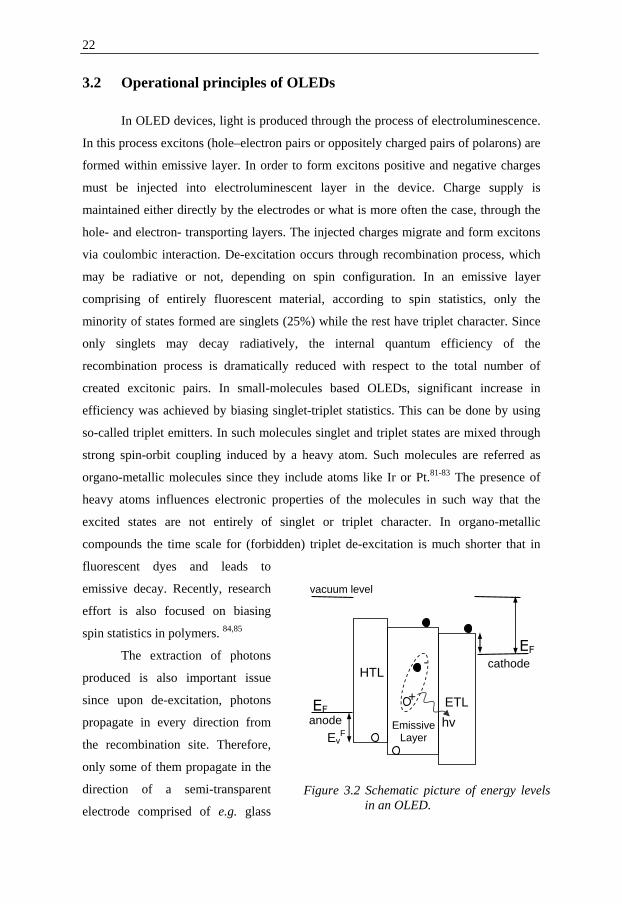
3.3 The role of interfaces for charge injection
As can be deduced from Fig. 3.2 the electronic level alignment at the interfaces
sets the conditions for the injection of charges in a device like e.g. OLED. Often, in
organic diodes there are electronic level misalignments at the interfaces, which lead to
the contact-limited injection regime. There are mainly two reasons for this situation.
First of them is the mismatch between work function of the electrode and ionization
potential (electron affinity) of the material in organic film, as shown in figure 3.3.
Another is the presence of additional barriers between organic layers e.g. HTL and
active layer.
In both cases presented in figure 3.3, a common vacuum level is assumed. The position
of Fermi level versus vacuum level is given by the work function φs of anode (cathode).
Work function can be easily obtained by photoelectron spectroscopy as well as the
threshold ionization potential (IP) of a molecule. In this way the hole-injection barrier
can be estimated. In the case of electron injection barrier information of un-occupied
states is needed, which can be provided by inverse photoemission spectroscopy. On this
example, one can deduce that in order to obtain possibly barrier-less injection across the
interface, the magnitude of the work function of an electrode should be (if possible)
equal IP of organic material (or EA in the case electron injection). However, as shown
by Seki et al. this simple picture often does not hold.38
Figure 3.3 The schematic picture showing the energy level alignment at the interface of an electrode and organic layer. In these cases vacuum level alignment is assumed.
HOMO
φs
EF
EA
EvF
LUMO
EVAC
IP
anode
LUMO
HOMO
φs
EF
EA
ECF
EVAC
cathode
25
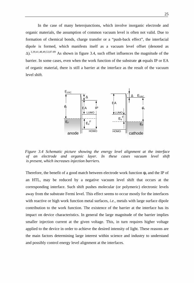
In the case of many heterojunctions, which involve inorganic electrode and
organic materials, the assumption of common vacuum level is often not valid. Due to
formation of chemical bonds, charge transfer or a “push-back effect”, the interfacial
dipole is formed, which manifests itself as a vacuum level offset (denoted as
∆).3,39,41,48,49,53,87-89 As shown in figure 3.4, such offset influences the magnitude of the
barrier. In some cases, even when the work function of the substrate φs equals IP or EA
of organic material, there is still a barrier at the interface as the result of the vacuum
level shift.
Therefore, the benefit of a good match between electrode work function φS and the IP of
an HTL, may be reduced by a negative vacuum level shift that occurs at the
corresponding interface. Such shift pushes molecular (or polymeric) electronic levels
away from the substrate Fermi level. This effect seems to occur mostly for the interfaces
with reactive or high work function metal surfaces, i.e., metals with large surface dipole
contribution to the work function. The existence of the barrier at the interface has its
impact on device characteristics. In general the large magnitude of the barrier implies
smaller injection current at the given voltage. This, in turn requires higher voltage
applied to the device in order to achieve the desired intensity of light. These reasons are
the main factors determining large interest within science and industry to understand
and possibly control energy level alignment at the interfaces.
Figure 3.4 Schematic picture showing the energy level alignment at the interface of an electrode and organic layer. In these cases vacuum level shift is present, which increases injection barriers.
HOMO
EA
EvF
∆
LUMO
IP φs
EF
EVAC
HOMO
φs
EF
EA
EvF
LUMO
EVAC ∆
anode cathode
26
There are several different approaches to engineer an interface of desired properties.
First of all for anode side of the device, the electrode used is almost always ITO, which
has relatively high work function but still lower than IP of the most of the HTLs.40
Therefore various HTLs materials have been studied in order to provide the best match
between energy levels.72 On the other hand, by the modification of the surface of ITO,
the work function can be significantly increased.42,90-95 In paper III, it is shown however,
that the hole-injection barriers can be reduced by increasing the work function of a
substrate only to certain point. As the work function of the substrate exceeds the energy
of integer charge transfer state (ICTS), the interfacial dipole is formed. The magnitude
of the dipole scales linearly with φs, while at the same time the barriers for hole-
injection remain constant. Any further increase in φs has little (if any) effect on the
charge injection barrier, but results instead in an interfacial dipole layer. The
conclusions presented in paper III are based on UPS results obtained on various
molecular semiconductors: CBP (4,4′-N,N′-dicarbazolyl-biphenyl), NPB (N,N′-bis-(1-
naphthyl)-N,N′-diphenyl1-1,1-biphenyl1-4,4-diamine), and m-MTDATA (4,4,4″-tris[3-
methyl-phenyl(phenyl)amino]-triphenylamine). The observed alignment regimes find
correspondence to the charge injection characteristics.96 The nature of ICTS is further
studied in paper IV with the aid of photoelectron spectroscopy. In order to interpret the
experimental data the theoretical calculations have been also performed. In paper V,
photoelectron studies of multi-layered systems comprising of two organic materials and
the substrate are reported. One of the important conclusions is that the alignment of
energy levels depends on the equilibration of the chemical potential throughout the
entire layer stack, while any specific electronic coupling between the individual layers
is of lesser importance. The results presented show also that the equality of interface
energetics under reversal of deposition sequence is not always a valid assumption.
These findings should be helpful in designing of multilayer structures in organic-based
charge injection/extraction devices (e.g. OLEDs).

27
44
Quantum chemical calculations
In this chapter a very brief description of Density Functional Theory (DFT) is
given. The quantum chemical calculations, based on DFT, have been performed for the
sake of interpretation of photoelectron spectra in paper IV.
4.1 Density Functional Theory (DFT)
Calculations based on Density Functional Theory can provide in-depth
information about electronic and chemical structure of an organic system.97 The theory
focuses on electron density ρ(r) as the most important quantity from which the ground
state wavefunction and the expectation value of any electronic property of the system
can be obtained. DFT is based on Hohenberg-Kohn theorems,98 which say that: (i) there
is a correspondence between the ground state electron density and the ground state
wavefunction of a many-particle system; (ii) the ground state electronic density
minimizes the total energy of the system. The DFT became really useful for
computational chemistry when Kohn and Sham introduced the formalism incorporating
orbitals.99
The important feature of DFT method is that it incorporates electron correlation effects:
(i) coulombic correlation, which is associated with the coulombic repulsion force
28
HOMO-1
HOMO
LUMO
NC
F F
F F
CN
CN
NC
Figure 4.2 (a) Chemical structure of tetrafluoro-tetracyanoquinodimethane (F4-TCNQ), (b) a visualization of electronic orbitals based on DFT calculations.
between electrons and (ii) exchange correlation, which is related to the Fermionic nature
of electrons and originates from Pauli exclusion principle. The DFT concepts can be
also extended to the time-dependent description of an electronic system, which is useful
in the study of various excitation processes.
4.2 Theoretical results versus photoelectron spectra
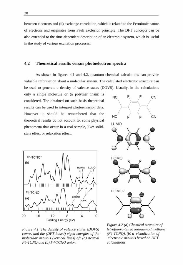
As shown in figures 4.1 and 4.2, quantum chemical calculations can provide
valuable information about a molecular system. The calculated electronic structure can
be used to generate a density of valence states (DOVS). Usually, in the calculations
only a single molecule or (a polymer chain) is
considered. The obtained on such basis theoretical
results can be used to interpret photoemission data.
However it should be remembered that the
theoretical results do not account for some physical
phenomena that occur in a real sample, like: solid-
state effect or relaxation effect.
Figure 4.1 The density of valence states (DOVS) curves and the (DFT-based) eigen-energies of the molecular orbitals (vertical lines) of: (a) neutral F4-TCNQ and (b) F4-TCNQ anion.
20 16 12 8 4 0
F4-TCNQ-
F4-TCNQ
Binding Energy (eV)
HOMO LUMO
HOMO α, β
LUMO α, β
(a)
(b)
29
55
Experimental technique
Photoelectron spectroscopy is one of the most powerful experimental techniques
used in the studies of materials. As the name already suggests, this technique is based
on photoelectric effect observed by Hertz in 1887 and then theoretically explained by
Einstein in 1905. Since the first observation of the core level lines, the technique has
evolved together with development of instrumentation and advances in science. During
1960s a high-resolution spectrometer has been developed by Kai Siegbahn and co-
workers.100 Since then, the details of electron binding energy could be studied with the
aid of well-resolved spectra. This achievement has led to the new application of
photoelectron spectroscopy: chemical analysis, often called ESCA (Electron
Spectroscopy for Chemical Analysis). Due to the good resolution of photoemission
spectra the technique can provide wide range of useful information not only concerning
atomic composition of the samples but also their physical and chemical properties. Over
the years, the scope of the photoelectron studies has significantly broadened. Many
different scientific topics have been studied, to mention a few: electronic structure of
organic molecular materials in solid and gas phase, surfaces and interfaces of thin
molecular and polymeric films, polymer blends, doped molecular and polymeric
systems, adsorbates and many more. 1,2,51,101-113
30
5.1 Background information
Photoionization occurs upon interaction of light (photons) with electrons. In this
process the law of conservation energy imposes conditions that govern generation of
photoelectrons. The magnitude of kinetic energy of the electrons that are ejected from
the sample upon photoionization process, carries information about studied sample e.g.
atoms, molecules, polymers, etc. In order to extract this information the kinetic energy
distribution of photoelectrons is acquired in the form of spectrum. The kinetic energy of
emitted electrons is dependent on photon energy and the energy change induced in the
system (e.g. atom, molecule). This relation has the form as follows:
hν + EG = EK + E+*, (5.1.1)
where: hν is the photon energy, EG stands for the total energy of the neutral atom
(molecule) in its ground state, EK accounts for the kinetic energy of the photoelectron
and E+* is the total energy of the ionized specie (atom, molecule) that is left after
electron emission.
In the equation 5.1.1, two parameters describe the energetic states of the system namely
EG and E+. The first relates to the state before the photionization event while the second
corresponds to the final state of the system that is without electron. Consequently the
difference between these two quantities directly relates to the energy “consumed” to
photoionize the system. This energy is often denoted as the binding energy of an
electron:
EB = E+ - EG. (5.1.2)
Hence the equation 5.1.2 can be written in the form as follows:
EB = hν - EK. (5.1.3)
When the incident photon energy is known, the binding energy of a certain
photoelectron can be obtained by measuring its kinetic energy. The spectrum
representing the kinetic energy distribution of the photoelectrons is measured, which is
31
complete information obtained in photoelectron spectroscopy. For a given energy of
photons, the lower binding energy of the electron in the system the higher kinetic
energy has this electron upon photoionization. For a particular excitation energy (photon
energy) a photoelectron spectrum can be referred either to the kinetic or binding energy
of electrons.
The obtained photoemission spectrum is correlated to the distribution of the final states
of the system, e.g. molecule, polymer. Various final states are possible and derive from
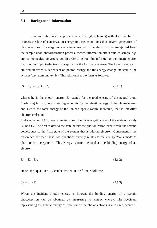
the electronic structure of an atom, molecule, polymer etc. In figure 5.1 the final states
configurations are schematically shown.
Case (a) corresponds to the photoionization of the least bound electron. The lowest
photon energy, which is sufficient for this process to occur, is referred as the on-set
ionization energy. In the case (b), an electron from a deeper level, hence having larger
binding energy, is ejected. So far discussed cases correspond to the final states
represented by a single hole created in the direct photoelectron emission. However,
more complicated scenarios are possible and give contribution observed in
photoelectron spectra as well. In shake-up processes (c), photoionization is
(d) (b)
Figure 5.1 A schematic representation of various final states created in a system upon photoionization.
on-set ionizatio
E0 E+ E+
unoccupied levels
occupied valence levels
core-level ionization
ground state
shake-off
E+*
shake-up
E+*
core levels
(a) (c)
32
accompanied by promotion of another electron to a previously unoccupied electronic
level. To satisfy energy conservation rule, the kinetic energy of the photoelectron
escaping from the sample is reduced by ∆E*:
EK = hν - EB - ∆E*. (5.1.4)
In shake-up the final state constitutes of core-hole and excited electron in valence level.
Photoionization can lead also to promotion of another electron to the continuum of
unbound states. Such a process is called shake-off (d) and corresponds to a doubly
ionized system as the final state.
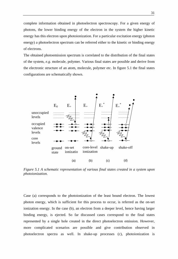
The features observed in the photoelectron spectrum (figure 5.2) correspond to the
previously discussed final states. The most intense peaks originate from photoelectrons
corresponding to the final state with a single core hole only. The small peak observed on
the lower kinetic energy side of C2 derives from shake-up. The shake-off process
contributes to the background observed on the lower kinetic energy side of the main
line. The probability of additional electronic excitation that leads to shake-up or shake-
Binding Energy (eV)
C2-∆E*
C2
C1
kinetic energy measured (eV) (photoelectron spectrum)
∆E*
C2 C1
core levels
valence levels
V1V2V3
V1V2V3
empty levels
Figure 5.2 The schematic picture of the photoelectron spectra and its correspondence to the electronic structure.
33
off depends on the electronic structure of an investigated system. Nevertheless the most
probable final state is a single hole final state, which gives the strongest contribution to
PES spectrum. Apart of shake-off, there are other contributions that lead to the observed
background. After an electron is emitted upon excitation from electromagnetic field of
incoming photon, it propagates in the solid. On its way to the surface it can experience
inelastic and elastic scattering. This, in turn, leads to the decrease in the initial kinetic
energy. The probability of scattering rises as photoelectron path to the surface increases.
As a result of scattering an emitted photoelectron may never approach the surface and
its kinetic energy may be totally dissipated. This implies certain limitations to the
photoelectron technique.114
The mean free path of electrons propagating in the sample determines the depth
from which photoelectrons can escape from the sample undisturbed. The inelastic
scattering leads to the so-called secondary electrons, which either contribute to the
spectrum in the form of background or are not detected since they remain in the sample.
The mean free path in a solid sample depends on the kinetic energy of photoelectrons.
Since the kinetic energy of the emitted electrons depends on the excitation energy, the
probing depth also varies significantly for different excitation energies. Even for high
kinetic energy electrons (Ek>1keV) the mean free path does not exceeds 100Å, which
makes photoelectron spectroscopy a very surface sensitive method.
5.2 The theory of photoelectron emission
The photoelectron emission in a solid sample is often considered as a three-step
process. First step includes the interaction between photon and a bound electron, which
leads to photoexcitation of the electron. This process is followed by perturbed
(dissipation of kinetic energy) or unperturbed propagation of electron in the solid.
Relevant to this work, however, are only electrons traveling towards the surface, since
they take part in the final step, which is penetration through the surface into the vacuum.
Photoexcitation can be described by transition probability σ. For a perturbation ∆, the
transition probability σ between initial states is characterized by the wave function ψi
and final states f with the wave function ψf, is given by Fermi’s Golden Rule:

34
( )ωδπσ hh
−−∆∝ if EEif22
. (5.2.1)
The operator ∆ can be expressed in terms of the vector potential A and the momentum
operator p through the formula:
pA omc
e=∆ . (5.2.2)
In the simplest picture, the assumption of one-electron wavefunction in initial and final
state is made with free electron characterized by kinetic energy EK. The initial-state and
the final-state wavefunctions: ψi(N) and ψf(N), can be expressed as the product of
orbital фk from which the electron is excited and the wavefunction of remaining
electrons is kRi ,ψ :
)1()( ,, −= NCN kRikii ψφψ . (5.2.3)
Similar expression describes the final-state wavefunction:
)1()( ,, −= NCN kRfEkinff ψφψ , (5.2.4)
where in both cases C is the operator that antysymmetrizes the wave functions.
Hence the transition matrix element from equation 5.2.1 is obtained as:
)1(|)1(|||| ,,,, −−= NNrr kRi
kRfkiEkinfif ψψφφψψ . (5.2.5)
Under the assumption that the orbitals are the same before and after the photoionization,
the electron overlap integral would be unity. In such a case the transition matrix element
consists only of one-electron contributions. This approximation neglects however
relaxation effect, which occurs upon release of an electron. The remaining (N-1)
electrons rearrange in order to screen the hole created in photoionization process, which
minimizes the total energy of the system. In order to express the photoemission intensity
I, equations 5.2.1 and 5.2.5, are combined to give the formula:
35
2
,, ,,,,
2
,, )1(|)1(||∑ ∑ −−∝kif nif
kRi
knfkiEkinf NNrI ψψφφ (5.2.6)
( ) ( )( )ωδ h−−−+× NENEE nkinf 0, 1
Photoionization from a particular orbital k gives rise to the line in kinetic energy
photoelectron spectrum. If there is more than one possible final state it is manifested by
set of satellites according to the probability distribution of these states.114
5.3 XPS - core level spectroscopy
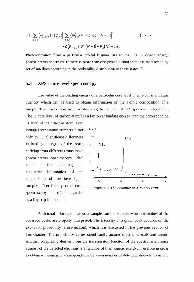
The value of the binding energy of a particular core level in an atom is a unique
quantity which can be used to obtain information of the atomic composition of a
sample. This can be visualized by observing the example of XPS spectrum in figure 5.3
The 1s core level of carbon atom has a far lower binding energy than the corresponding
1s level of the nitrogen atom, even
though their atomic numbers differ
only by 1. Significant differences
in binding energies of the peaks
deriving from different atoms make
photoelectron spectroscopy ideal
technique for obtaining the
qualitative information of the
composition of the investigated
sample. Therefore photoelectron
spectroscopy is often regarded
as a finger-print method.
Additional information about a sample can be obtained when intensities of the
observed peaks are properly interpreted. The intensity of a given peak depends on the
excitation probability (cross-section), which was discussed in the previous section of
this chapter. The probability varies significantly among specific orbitals and atoms.
Another complexity derives from the transmission function of the spectrometer, since
number of the detected electrons is a function of their kinetic energy. Therefore in order
to obtain a meaningful correspondence between number of detected photoelectrons and
N1s
C1s
Figure 5.3 The example of XPS spectrum.
36
the actual chemical composition of a sample, the sensitivity factor that provides
appropriate scaling for the photoelectron peaks intensities, are used.
Binding energy of the observed photoelectrons depends also on chemical
environment of their origin atom.115 When an atom is a part of a molecule or polymer,
the binding energy of its particular core level is affected by the density of valence
electrons localized close to the atom. This local density of charge is called “an effective
charge”. Even for the same atoms, an effective electronic charge can be different due to
the different chemical environment. This effect is often pronounced in the photoelectron
spectra and is called a chemical shift. In molecular or polymeric systems, strongly
electronegative atoms withdraw electronic density from the less electronegative ones.
This, in turn is manifested by a change in the effective charge. Therefore the described
effect can be seen as the one that influences the initial state of an atom in terms of its
charge. The simple hypothesis, that the binding energy should be a function of such an
effective charge, has been shown to be a very good model to explain the differences
observed in binding energy of photoelectrons. On the other hand, binding energy of
electron is referred to as the energy difference between the ground and a final state.
Hence the chemical shift can be also discussed in terms of the different conditions for
creation of core hole. Intuitively, the higher electronic charge density on the atom
should correspond to a decrease of the required energy to create a core-hole.
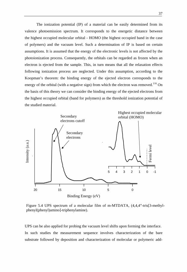
5.4 UPS - spectroscopy of valence levels
In ultra-violet photoelectron spectroscopy (UPS) the often used source of
photons is HeI radiation of energy hv=21.2eV or HeII radiation (hv=40.8eV). These
photon energies allow for mapping out the valence electronic states of a molecular or
polymeric sample. The UPS spectra can provide valuable information not only about
details of the electronic structure of the studied material but also about its work
function φ, and also the ionization potential (IP).
Work function is a very important parameter, which determines the minimum
energy necessary to remove an electron from the material. When the energy of photons
hv is known (for HeI source - 21.2eV), the work function can be obtained from the
measured energy of the secondary electron cutoff (Ecutoff) (see Fig. 5.4). The simple
formula for obtaining work function has a form as follows: φ = hv - Ecutoff .
37
.
5 4 3 2 1 0 -1
The ionization potential (IP) of a material can be easily determined from its
valence photoemission spectrum. It corresponds to the energetic distance between
the highest occupied molecular orbital - HOMO (the highest occupied band in the case
of polymers) and the vacuum level. Such a determination of IP is based on certain
assumptions. It is assumed that the energy of the electronic levels is not affected by the
photoionization process. Consequently, the orbitals can be regarded as frozen when an
electron is ejected from the sample. This, in turn means that all the relaxation effects
following ionization process are neglected. Under this assumption, according to the
Koopman’s theorem: the binding energy of the ejected electron corresponds to the
energy of the orbital (with a negative sign) from which the electron was removed.116 On
the basis of this theory we can consider the binding energy of the ejected electrons from
the highest occupied orbital (band for polymers) as the threshold ionization potential of
the studied material.
UPS can be also applied for probing the vacuum level shifts upon forming the interface.
In such studies the measurement sequence involves characterization of the bare
substrate followed by deposition and characterization of molecular or polymeric add-
.
20 15 10 5 0
Binding Energy (eV)
Secondary electrons
Secondary electrons cutoff
Highest occupied molecular orbital (HOMO)
Inte
nsity
(a.
u.)
Fer
mi l
evel
Figure 5.4 UPS spectrum of a molecular film of m-MTDATA, (4,4,4″-tris[3-methyl-phenyl(phenyl)amino]-triphenylamine).
38
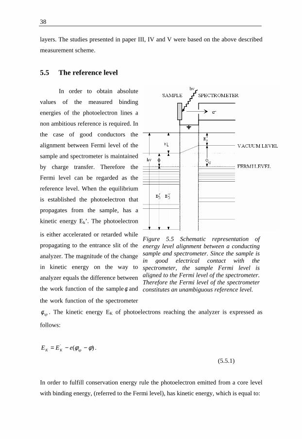
layers. The studies presented in paper III, IV and V were based on the above described
measurement scheme.
5.5 The reference level
In order to obtain absolute
values of the measured binding
energies of the photoelectron lines a
non ambitious reference is required. In
the case of good conductors the
alignment between Fermi level of the
sample and spectrometer is maintained
by charge transfer. Therefore the
Fermi level can be regarded as the
reference level. When the equilibrium
is established the photoelectron that
propagates from the sample, has a
kinetic energy Ek’. The photoelectron
is either accelerated or retarded while
propagating to the entrance slit of the
analyzer. The magnitude of the change
in kinetic energy on the way to
analyzer equals the difference between
the work function of the sampleφ and
the work function of the spectrometer
spφ . The kinetic energy EK of photoelectrons reaching the analyzer is expressed as
follows:
)(' φφ −−= spKK eEE .
(5.5.1)
In order to fulfill conservation energy rule the photoelectron emitted from a core level
with binding energy, (referred to the Fermi level), has kinetic energy, which is equal to:
Figure 5.5 Schematic representation of energy level alignment between a conducting sample and spectrometer. Since the sample is in good electrical contact with the spectrometer, the sample Fermi level is aligned to the Fermi level of the spectrometer. Therefore the Fermi level of the spectrometer constitutes an unambiguous reference level.
39
FBK EehvE −−= φ' . (5.5.2)
By combining equations (5.5.1) and (5.5.2) the formula for kinetic energy of
photoelectron reaching the analyzer is expressed through the photoelectron’s binding
energy, referred to the Fermi level, as follows:
spFBK eEhvE φ−−= . (5.5.3)
Hence, when the photon energy and the spectrometer work function are known, the
measurement of photoelectrons kinetic energy can be related to the binding energy of
the emitted electrons relative to the Fermi level. The photoelectrons originating from
given core level will always appear in the spectrometer with the same kinetic energy
regardless to the work function of the sample (under assumption that the photon energy
is kept constant).
In the case when the sample is poorly conductive the positive charges created
upon photoionization process cannot be neutralized. In such a case the assumption of
common Fermi level of the sample and the spectrometer is not valid. During the
measurement uncompensated positive charges accumulate in the sample, which is often
referred as charging. In this situation Fermi level of the sample is shifted versus that of
the spectrometer in such a way that the measured binding energy is always higher than
in the case when the charge flow is sufficient to maintain sample neutrality. Enhancing
compensation rate of positive charges might solve the problem of charging. This can be
done by using an external source of electrons, such as an electron flood gun.

40
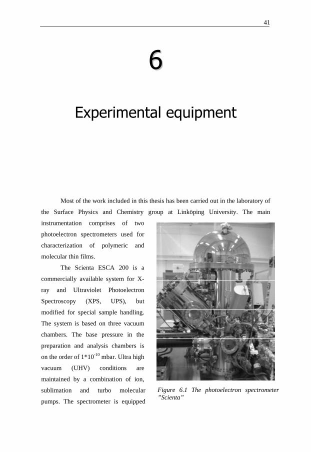
41
66
Experimental equipment
Most of the work included in this thesis has been carried out in the laboratory of
the Surface Physics and Chemistry group at Linköping University. The main
instrumentation comprises of two
photoelectron spectrometers used for
characterization of polymeric and
molecular thin films.
The Scienta ESCA 200 is a
commercially available system for X-
ray and Ultraviolet Photoelectron
Spectroscopy (XPS, UPS), but
modified for special sample handling.
The system is based on three vacuum
chambers. The base pressure in the
preparation and analysis chambers is
on the order of 1*10-10 mbar. Ultra high
vacuum (UHV) conditions are
maintained by a combination of ion,
sublimation and turbo molecular
pumps. The spectrometer is equipped
Figure 6.1 The photoelectron spectrometer ”Scienta”
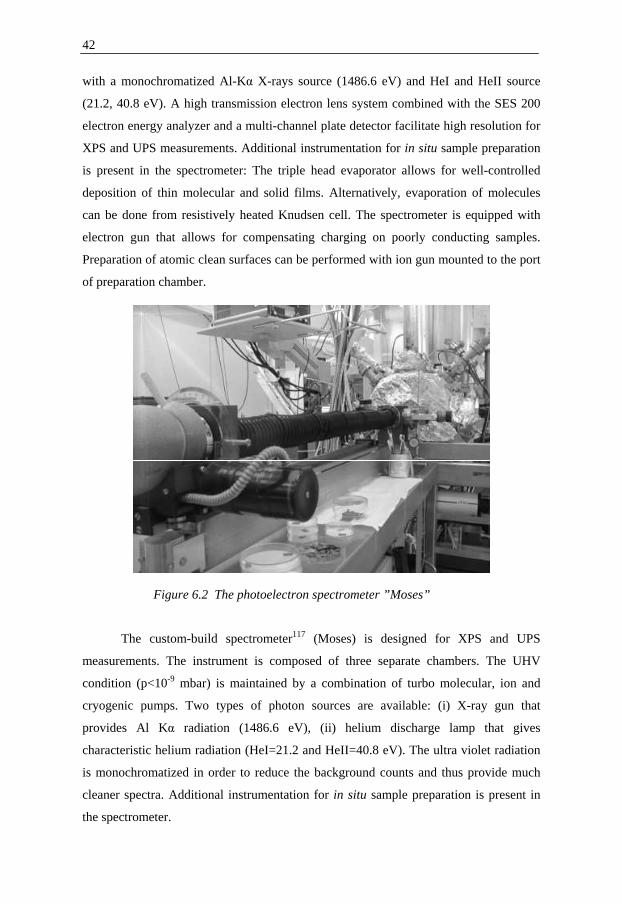
42
with a monochromatized Al-Kα X-rays source (1486.6 eV) and HeI and HeII source
(21.2, 40.8 eV). A high transmission electron lens system combined with the SES 200
electron energy analyzer and a multi-channel plate detector facilitate high resolution for
XPS and UPS measurements. Additional instrumentation for in situ sample preparation
is present in the spectrometer: The triple head evaporator allows for well-controlled
deposition of thin molecular and solid films. Alternatively, evaporation of molecules
can be done from resistively heated Knudsen cell. The spectrometer is equipped with
electron gun that allows for compensating charging on poorly conducting samples.
Preparation of atomic clean surfaces can be performed with ion gun mounted to the port
of preparation chamber.
The custom-build spectrometer117 (Moses) is designed for XPS and UPS
measurements. The instrument is composed of three separate chambers. The UHV
condition (p<10-9 mbar) is maintained by a combination of turbo molecular, ion and
cryogenic pumps. Two types of photon sources are available: (i) X-ray gun that
provides Al Kα radiation (1486.6 eV), (ii) helium discharge lamp that gives
characteristic helium radiation (HeI=21.2 and HeII=40.8 eV). The ultra violet radiation
is monochromatized in order to reduce the background counts and thus provide much
cleaner spectra. Additional instrumentation for in situ sample preparation is present in
the spectrometer.
Figure 6.2 The photoelectron spectrometer ”Moses”

43
77
References
1 W. R. Salaneck, S. Strafström, and J. L. Brédas, Conjugated polymer surfaces
and interfaces: electronic and chemical structure of interfaces for polymer light
emitting devices. (Cambridge Unversity Press, Cambridge, 1996). 2 W. R. Salaneck, R. H. Friend, and J. L. Brédas, Physics Reports 319, 231
(1998). 3 W. R. Salaneck and J. L. Brédas, Adv. Mater. 8, 48 (1996). 4 W. R. Salaneck, K. Seki, A. Kahn, and J.-J. Pireaux, Conjugated polymer and
molecular interfaces: Science and technology for photonic and optoelectronic
applications (Marcel Dekker, New York, 2002). 5 N. Sato and M. Yoshikawa, J. Elec. Spec. Rel. Phen. 78, 387 (1996). 6 H. Shirakawa, E. J. Louis, A. G. MacDiarmid, C. K. Chiang, and A. J. Heeger,
Chem. Comm., 578 (1977). 7 C. K. Chiang, C. R. Fincher, Y. W. Park, A. J. Heeger, H. Shirakawa, E. J.
Louis, S. C. Gau, and A. G. MacDiarmid, Phys. Rev. Lett. 39, 1098 (1977). 8 C. W. Tang, Appl. Phys. Lett. 48, 183 (1986). 9 P. Peumans, V. Bulovic, and S. R. Forrest, Appl. Phys. Lett. 76, 3885 (2000). 10 A. Bandhopadhyay and A. J. Pal, J. Phys. Chem. B 107, 2531 (2003). 11 W. C. Chih, J. Y. Ouyang, J. H. Tseng, and Y. Yang, Adv. Mater. 15, 1440
(2005).

44
12 B. K. Crone, A. Dodabalapur, R. Sarpeshkar, A. Gelperin, H. E. Katz, and Z.
Bao, J. Appl. Phys. 91, 10140 (2002). 13 T. W. G. Solomons and C. B. Fryhle, Organic Chemistry (John Wiley & Sons,
New York, 1998). 14 W. R. Salaneck and J. L. Brédas, Solid State Communications 92, 31-6 (1994). 15 R. E. Peierls, Quantum Theory of Solids (Oxford University Press, London,
1955). 16 C. S. Yannoni and T. C. Clarke, Phys. Rev. Lett. 51, 1191 (1983). 17 W. P. Su, J. R. Schrieffer, and A. J. Heeger, Phys. Rev. Lett. 42, 1698 (1979). 18 W. P. Su, J. R. Schrieffer, and A. J. Heeger, Phys. Rev. B. 22, 2099 (1980). 19 N. Suzuki, M. Ozaki, S. Etemad, A. J. Heeger, and M. G. MacDiarmid, Phys.
Rev. Lett. 45, 1209 (1980). 20 S. Stafström and J. L. Brédas, Phys. Rev. B. 38, 4180 (1988). 21 A. J. Heeger, Angew. Chem. Int. Ed. 40, 2591 (2001). 22 H. W. Heuer, R. Wehrmann, and S. Kirchmeyer; Adv. Func. Mater. 12 (2002)
89. 23 B. Sankaran and J. R. Reynolds; Macromolecules, 30, 2582 (1997). 24 J. Lu, N. J. Pinto, and A. G. MacDiarmid, 92 (2002). 25 J. Blochwitz, Synth. Met. 127, 169 (2002). 26 W. Gao and A. Kahn, Org. Electron. 3, 53(2002). 27 W. Gao, J. Appl. Phys. 94, 359 (2003). 28 W. Gao, J. Phys. Condens. Matter 15, S2757 (2003). 29 L. Groenendaal, F. Jonas, D. Freitag, H. Pielartzik, and J. R. Reynolds, Adv.
Mater. 12, 481 (2000). 30 A. Elschner, F. Bruder, H.-W. Heuer, F. Jonas, A. Karbach, S. Kirchmeyer, S.
Thurn, and R. Wehrmann, Synth. Met. 111-112, 139 (2000). 31 W. H. Kim, A. J. Mäkinen, N. Nikolov, R. Shashidhar, H. Kim, and Z. H.
Kafafi, Appl. Phys. Lett. 80, 3844 (2002). 32 J. Lu, N. J. Pinto, and A. G. MacDiarmid, J. Appl. Phys. 92, 6033 (2002). 33 A. C. Arias, M. Granström, D. S. Thomas, K. Petritsch, and R. H. Friend, Phys.
Rev. B. 60, 1854 (1999). 34 A. N. Aleshin, R. Kiebooms, and A. J. Heeger, Synth. Met. 101, 369 (1999). 35 Bayer, in Eur. Patent (1988), p. 339. 36 N. Koch and A. Vollmer, Appl. Phys. Lett. 89, 162107 (2006).
45
37 C. Tengstedt, A. Kanciurzewska, M. P. d. Jong, S. Braun, W. R. Salaneck, and
M. Fahlman, Thin Solid Films 515, 2085 (2006). 38 K. Seki, E. Ito, and H. Ishii, Synth. Met. 91, 137 (1997). 39 J. Blochwitz, T. Fritz, M. Pfeiffer, K. Leo, D. M. Alloway, P. A. Lee, and N. R.
Armstrong, Org. Elect. 2, 97 (2001). 40 L. Chkoda, Synth. Met. 111, 315 (2000). 41 X. Crispin, V. Geskin, A. Crispin, J. Cornil, R. Lazzaroni, W. R. Salaneck, and
J.-L. Brédas, J. Am. Chem. Soc. 124, 8131(2002). 42 C. Ganzorig, K.-J. Kwak, K. Yagi, and M. Fujihiraa, Appl. Phys. Lett. 79, 272
(2001). 43 W. Gao and A. Kahn, Appl. Phys. Lett. 82, 4815 (2003). 44 I. G. Hill and A. Kahn, J. Appl. Phys. 84, 5583 (1998). 45 I. G. Hill, D. Milliron, J. Schwartz, and A. Kahn, Appl. Surf. Sci. 166, 354
(2000). 46 I. G. Hill, A. Rajagopal, and A. Kahn, J. Appl. Phys. 84, 3236 (1998). 47 I. G. Hill, A. Rajagopal, A. Kahn, and Y. Hu, Appl. Phys. Lett. 73, 662 (1998). 48 H. Ishii, Journal of Luminescence 87, 61 (2000). 49 H. Ishii, K. Sugiyama, E. Ito, and K. Seki, Adv. Mater. 11, 605 (1999). 50 E. Ito, H. Oji, N. Hayashi, H. Ishii, Y. Ouchi, and K. Seki, Appl. Surf. Sci. 175-
176, 407 (2001). 51 A. Kahn, N. Koch, and W. Gao, J. Polym. Sci., Polym. Phys. 41, 2529 (2003). 52 A. Kahn, W. Zeo, W. Gao, H. Vázquez, and F. Flores, Chem. Phys. 325, 129
(2006). 53 S. Kera, Y. Yabuuchi, H. Yamane, H. Setoyama, K. K. Okudaira, A. Kahn, and
N. Ueno, Phys. Rev. B 70, 085304 (2004). 54 N. Koch, S. Duhm, J. P. Rabe, A. Vollmer, and R. L. Johnson, Phys. Rev. Lett.
95, 237601 (2005). 55 N. Koch, A. Kahn, J. Ghijsen, J.-J. Pireaux, J. Schwartz, R. L. Johnson, and A.
Elschner, Appl. Phys. Lett. 82, 70 (2003). 56 R. J. Murdey and W. R. Salaneck, Jpn. J. Appl. Phys 44, 3751 (2005). 57 S. M. Tadayyon, Org. Electron. 5, 157 (2004). 58 G. Heimel, L. Romaner, E. Zojer, and J. L. Brédas, Nano Letters 7, 932 (2007). 59 A. Rajagopal, C. I. Wu, and A. Kahn, J. Appl. Phys. 83, 2649 (1998). 60 A. Rajagopal and A. Kahn, Adv. Mater. 10, 140 (1998).

46
61 H. Vázquez, F. Flores, R. Oszwaldowski, J. Ortega, R. Perez, and A. Kahn,
Appl. Surf. Sci. 234, 107 (2004). 62 H. Vázquez, W. Gao, F. Flores, and A. Kahn, Phys. Rev. B 71, 041306 (2005). 63 H. Vázquez, F. Flores, and A. Kahn, Org. Electron. 8, 241 (2007). 64 C. Tengstedt, W. Osikowicz, W. R. Salaneck, I. D. Parker, C.-H. Hsu, and M.
Fahlman, Appl. Phys. Lett. 88, 053502 (2006). 65 A. Crispin, X. Crispin, M. Fahlman, M. Berggren, and W. R. Salaneck, Appl.
Phys. Lett. 89, 213503 (2006). 66 S. Braun, W. Osikowicz, Y. Wang, and W. R. Salaneck, Org. Electron. 8, 14
(2007). 67 C. W. Tang and S. A. VanSlyke, Appl. Phys. Lett. 51, 913 (1987). 68 C. W. Tang, S. A. VanSlyke, and C. H. Chen, J. Appl. Phys. 65, 3610 (1989). 69 C. Adachi, K. Nagai, and N. Tamoto, Applied Physics Letters 66, 2679-2681
(1995). 70 C. Adachi, S. Tokito, T. Tsutsui, and S. Saito, Jpn. J. Appl. Phys. 27, L269
(1988). 71 C. Adachi, S. Tokito, T. Tsutsui, and S. Saito, Jpn. J. Appl. Phys. 27, L713
(1988). 72 C. Giebeler, H. Antoniadis, D. D. C. Bradley, and Y. Shirota, J. Appl. Phys. 85,
608 (1999). 73 J. H. Burroughes, D. D. C. Bradley, A. R. Brown, R. N. Marks, K. Mackay, R.
H. Friend, P. L. Burns, and A. B. Holmes, Nature 347, 539 (1990). 74 R. H. Friend, R. W. Gymer, A. B. Holmes, J. H. Burroughes, R. N. Marks, C.
Taliani, D. D. C. Bradley, D. A. D. Santos, J. L. Brédas, M. Lögdlund, and W.
R. Salaneck, Nature 397, 121 (1999). 75 M. T. Bernius, M. Inbasekaran, J. O'Brien, and W. Wu, Adv. Mater. 12, 1737
(2000). 76 www.covion.com 77 F. Nuesch, L. J. Rothberg, E. W. Forsythe, Q. T. Le, and Y. Gao, Appl. Phys.
Lett. 74, 880 (1999). 78 R. B. H. Tahar, T. Ban, Y. Ohya, and Y. Takahashi, J. Appl. Phys. 83, 2631
(1998). 79 T. Osada, T. Kugler, P. Broms, and W. R. Salaneck, Synth. Met. 96, 77 (1998).

47
80 G. Gustafsson, Y. Cao, G. M. Treacy, F. Klavetter, and N. Col, Nature 357, 477
(1992). 81 M. A. Baldo, S. Lemansky, P. E. Burrows, M. E. Thompson, and S. R. Forrest,
Appl. Phys. Lett. 76, 4 (1999). 82 M. A. Baldo, D. F. O’Brien, M. E. Thompson, and S. R. Forrest, Phys. Rev. B.
66, 14422 (1999). 83 M. A. Baldo, D. F. O’Brien, Y. You, A. Shoustikov, S. Sibley, M. E. Thompson,
and S. R. Forrest, Nature 395, 151 (1998). 84 A. Kadashchuk, A. Vakhnin, I. Blonski, D. Beljonne, Z. Shuai, J. L. Brédas, V.
I. Arkhipov, P. Heremans, E. V. Emelianova, and H. Bässler, Phys. Rev. Lett.
93, 066803 (2004). 85 D. Beljonne, A. Ye, Z. Shuai, and J. L. Brédas, Adv. Funct. Mater. 14, 684
(2004). 86 P. W. M. Blom and M. C. J. M. Vissenberg, Rep. Mat. Sci.& Eng. 27, 53
(2000). 87 H. Peisert, M. Knupfer, F. Zhang, A. Petr, L. Dunsch, and J. Fink, Surf. Sci.
566-568, 554 (2004). 88 W. Osikowicz, X. Crispin, C. Tengstedt, L. Lindell, T. Kugler, and W. R.
Salaneck, Appl. Phys. Lett. 85, 1616 (2004). 89 A. J. Mäkinen, I. G. Hill, R. Shashidhar, N. Nikolov, and Z. H. Kafafi, Appl.
Phys. Lett. 79, 557 (2001). 90 S. Besbes, A. Ltaief, K. Reybier, L. Ponsonnet, N. Jaffrezic, J. Davenas, and H.
Ben Ouada, Synth. Met. 138, 197 (2003). 91 R. A. Hatton, S. R. Day, M. A. Chesters, and M. R. Willis, Thin Solid Films
394, 292 (2001). 92 P. K. H. Ho, M. Granstroem, R. H. Friend, and N. C. Greenham, Adv. Mat. 10,
769 (1998). 93 X. H. Sun, L. F. Cheng, M. W. Liu, L. S. Liao, N. B. Wong, C. S. Lee, and S. T.
Lee, Chem. Phys. Lett. 370, 425 (2003). 94 K. Sugiyama, H. Ishii, Y. Ouchi, and K. Seki, J. Appl. Phys. 87, 295 (2000). 95 C. C. Wu, C. I. Wu, J. C. Sturm, and A. Kahn, Appl. Phys. Lett. 70, 1348
(1997). 96 S. W. Tsang, S. C. Tse, K. L. Tong, and S. K. So, Org. Electron. 7, 474 (2006).

48
97 F. Jensen, Introduction to computational chemistry (John Wiley & Sons Ltd,
Chichester, 1999). 98 P. Hohenberger and W. Kohn, Phys. Rev. 136, B864 (1964). 99 W. Kohn and L. J. Sham, Phys. Rev. 140, A1133 (1965). 100 K. Siegbahn, ESCA; atomic, molecular and solid state structure studied by
means of electron spectroscopy (Uppsala, Almqvist & Wiksells, 1968). 101 W. R. Salaneck, CRC Critical Reviews in Solid State and Materials Sciences 12,
267 (1985). 102 W. R. Salaneck, Phys. Rev. Lett. 40, 60 (1978). 103 W. R. Salaneck, H. R. Thomas, R. W. Bigelow, C. B. Duke, E. W. Plummer, A.
J. Heeger, and A. G. MacDiarmid, J. Chem. Phys. 72, 3674 (1980). 104 W. R. Salaneck, H. R. Thomas, C. B. Duke, A. Paton, E. W. Plummer, A. J.
Heeger, and A. G. MacDiarmid, J. Chem. Phys. 71, 2044 (1979). 105 W. R. Salaneck, T. Kugler, A. Andersson, P. Bröms, J. Birgerson, and M.
Lögdlund, edited by J. L. Brédas (De Boeck & Larcier, Bruxelles, 1999), p. 43-
59. 106 M. Lögdlund, W. R. Salaneck, F. Meyers, J. L. Brédas, G. Arbuckle, R. H.
Friend, A. B. Holmes, and G. Froyer, Macromolecules 26, 3815 (1993). 107 M. P. d. Jong, R. Friedlein, S. L. Sorensen, G. Öhrwall, W. Osikowicz, M.
Fahlman, and W. R. Salaneck, Phys. Rev. B 72, 035448 (2005). 108 C. B. Duke, N. O. Lipari, W. R. Salaneck, and L. B. Schein, J. Chem. Phys. 63,
1758 (1975). 109 C. B. Duke, A. Paton, W. R. Salaneck, H. R. Thomas, E. W. Plummer, A. J.
Heeger, and A. G. MacDiarmid, Chem. Phys. Lett. 59, 146 (1978). 110 T. Kugler, A. Johansson, I. Dalsegg, U. Gelius, and W. R. Salaneck, Synth. Met.
91, 143 (1997). 111 G. Greczynski, M. Fahlman, W. R. Salaneck, N. Johansson, D. A. d. Santos, and
J. L. Brédas, Thin Solid Films 363, 322 (2000). 112 M. Fahlman, J. L. Brédas, and W. R. Salaneck, Synth. Met. 78(3), 237 (1996). 113 M. Lögdlund, G. Greczynski, A. Crispin, T. Kugler, M. Fahlman, and W. R.
Salaneck, in Conjugated Polymer and Molecular Interfaces: Science and
Technology for Photonic and Optoelectronic Application, edited by W. R.
Salaneck, K. Seki, A. Kahn, and J. J. Pireaux (Marcel Dekker, New York, 2002).

49
114 S. Hüfner, Photoelectron spectroscopy (Springer-Varlag, Berlin Heidelberg,
2003). 115 E. Sokolowski, C. Nordling, and K. Siegbahn, Phys. Rev. 110, 776 (1958). 116 T. A. Koopman, Physica 1, 104 (1933). 117 W. R. Salaneck, R. Bergman, J.-E. Sundgren, A. Rockett, T. Motooka, and J. E.
Greene, Surf. Sci. 198, 461 (1988).