Embed Size (px)
Citation preview
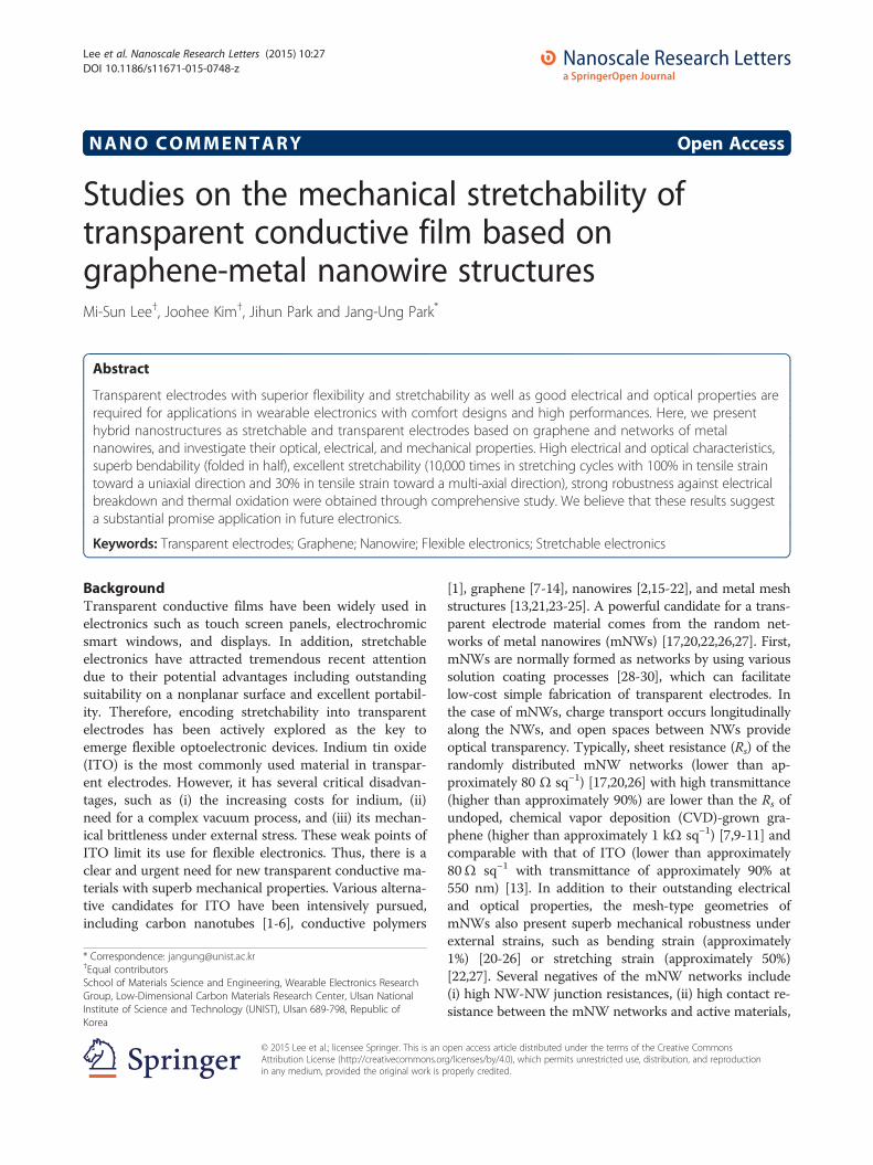
Lee et al. Nanoscale Research Letters (2015) 10:27 DOI 10.1186/s11671-015-0748-z
NANO COMMENTARY Open Access
Studies on the mechanical stretchability oftransparent conductive film based ongraphene-metal nanowire structuresMi-Sun Lee†, Joohee Kim†, Jihun Park and Jang-Ung Park*
Abstract
Transparent electrodes with superior flexibility and stretchability as well as good electrical and optical properties arerequired for applications in wearable electronics with comfort designs and high performances. Here, we presenthybrid nanostructures as stretchable and transparent electrodes based on graphene and networks of metalnanowires, and investigate their optical, electrical, and mechanical properties. High electrical and optical characteristics,superb bendability (folded in half), excellent stretchability (10,000 times in stretching cycles with 100% in tensile straintoward a uniaxial direction and 30% in tensile strain toward a multi-axial direction), strong robustness against electricalbreakdown and thermal oxidation were obtained through comprehensive study. We believe that these results suggesta substantial promise application in future electronics.
Keywords: Transparent electrodes; Graphene; Nanowire; Flexible electronics; Stretchable electronics
BackgroundTransparent conductive films have been widely used inelectronics such as touch screen panels, electrochromicsmart windows, and displays. In addition, stretchableelectronics have attracted tremendous recent attentiondue to their potential advantages including outstandingsuitability on a nonplanar surface and excellent portabil-ity. Therefore, encoding stretchability into transparentelectrodes has been actively explored as the key toemerge flexible optoelectronic devices. Indium tin oxide(ITO) is the most commonly used material in transpar-ent electrodes. However, it has several critical disadvan-tages, such as (i) the increasing costs for indium, (ii)need for a complex vacuum process, and (iii) its mechan-ical brittleness under external stress. These weak points ofITO limit its use for flexible electronics. Thus, there is aclear and urgent need for new transparent conductive ma-terials with superb mechanical properties. Various alterna-tive candidates for ITO have been intensively pursued,including carbon nanotubes [1-6], conductive polymers
* Correspondence: [email protected]†Equal contributorsSchool of Materials Science and Engineering, Wearable Electronics ResearchGroup, Low-Dimensional Carbon Materials Research Center, Ulsan NationalInstitute of Science and Technology (UNIST), Ulsan 689-798, Republic ofKorea
© 2015 Lee et al.; licensee Springer. This is an oAttribution License (http://creativecommons.orin any medium, provided the original work is p
[1], graphene [7-14], nanowires [2,15-22], and metal meshstructures [13,21,23-25]. A powerful candidate for a trans-parent electrode material comes from the random net-works of metal nanowires (mNWs) [17,20,22,26,27]. First,mNWs are normally formed as networks by using varioussolution coating processes [28-30], which can facilitatelow-cost simple fabrication of transparent electrodes. Inthe case of mNWs, charge transport occurs longitudinallyalong the NWs, and open spaces between NWs provideoptical transparency. Typically, sheet resistance (Rs) of therandomly distributed mNW networks (lower than ap-proximately 80 Ω sq−1) [17,20,26] with high transmittance(higher than approximately 90%) are lower than the Rs ofundoped, chemical vapor deposition (CVD)-grown gra-phene (higher than approximately 1 kΩ sq−1) [7,9-11] andcomparable with that of ITO (lower than approximately80Ω sq−1 with transmittance of approximately 90% at550 nm) [13]. In addition to their outstanding electricaland optical properties, the mesh-type geometries ofmNWs also present superb mechanical robustness underexternal strains, such as bending strain (approximately1%) [20-26] or stretching strain (approximately 50%)[22,27]. Several negatives of the mNW networks include(i) high NW-NW junction resistances, (ii) high contact re-sistance between the mNW networks and active materials,
pen access article distributed under the terms of the Creative Commonsg/licenses/by/4.0), which permits unrestricted use, distribution, and reproductionroperly credited.

Lee et al. Nanoscale Research Letters (2015) 10:27 Page 2 of 9
(iii) low breakdown voltages, (iv) poor adhesion of mNWsto flexible and plastic substrates, and (v) oxidation inharsh environments. These factors have limited their inte-gration as transparent electrodes in commercial optoelec-tronic devices [17,18,20-22,27].Another promising alternative to ITO comes in the form
of graphene that can be deformed up to a strain of approxi-mately 4% with negligible cracking [12] as well as absorbingonly approximately 2.3% of visible light [14]. In addition,the theoretical minimum Rs of pristine graphene has beenestimated to be as low as approximately 30 Ω sq−1 [31], butthe experimental Rs of undoped, synthesized graphene byusing various methods [7,8,10,11,32] is substantially higherthan the Rs of ITO. Although chemical doping processes[12,33] can further reduce Rs of the CVD-grown grapheneby increasing carrier density, the instability of the interac-tions between graphene and dopant typically limits thelifetime of this doping effect and leads to a time-variant in-crease of Rs [13].In this paper, we report graphene-mNW hybrid nano-
structures as high-performance, stretchable, and trans-parent electrodes. Especially, we focused on the study ofthe mechanical flexibility of the hybrid film, so variousflexible tests such as bending, folding, and uniaxial andmulti-axial directional stretching tests were performed.These fabricated hybrid structures present superb mech-anical flexibility (folding with bending radius of approxi-mately 3.7 μm) and stretchability (10,000 times in afatigue test with maximum stretching strain of 100% andstretching in tensile strain of 30% toward multi-axialdirection).
Experimental methodsSilver nanowires (AgNWs) with average length of 30 μm±7 μm and average diameter of 20 nm± 5 nm dispersed inethanol (3 mg mL−1) were purchased from Nanopyxis Co.,Ltd (Cheonan, South Korea). The solution was stored at5 °C, and then spin-coated on substrates. The spin coat-ing condition of AgNWs was fixed at 500 rpm for 30 s,except for the density study of AgNWs, which was doneaccording to the spin rates. After spinning the AgNWsuspension on substrates (with or without graphene as atop layer), the samples were annealed at 150 °C for 90 sto evaporate the solvent completely.The synthesis and transfer of graphene were carried
out under the following conditions. A Cu foil (AlfaAesar, item no. 13382; Ward Hill, MA, USA) was loadedonto the center of a quartz CVD reactor under low vac-uum (100 mTorr). Subsequently, the reactor was heatedup to 1,000 °C with introduction of the flow of Ar (200sccm) and H2 (500 sccm). The CVD growth was carriedout under CH4 (12 sccm) and H2 (500 sccm) flows for5 min, and then the reactor was rapidly cooled to roomtemperature under Ar (500 sccm) flow. To transfer the
synthesized graphene, we used a 200-nm-thick poly(me-thyl methacrylate) (Micro Chem Corp. 950 PMMA;Newton, MA, USA) film as a supporting layer which wasspun on the graphene. The Cu foil was dissolved in a di-luted etching solution of FeCl3:HCl:H2O (1:1:20 vol.%)with the PMMA/graphene layer floating on the surface ofthe solution. Subsequently, the sample was rinsed by float-ing it on the surface of deionized water (DI water) andthen the sample was transferred onto the desired sub-strates. In addition, the PMMA supporting layer was re-moved with acetone.We have employed two approaches to assemble the
hybrid structures (i) AgNWs on graphene or (ii) gra-phene on AgNWs: (i) After the CVD synthesis of thegraphene layer, the graphene was transferred onto a tar-get substrate. After spin casting of the AgNW disper-sions onto the graphene surface, this sample wasannealed at 150 °C for 90 s. (ii) AgNW network filmswere coated on substrate, as described above. Then thesynthesized graphene layer was transferred onto thefilms by using PMMA. Subsequently, the supportinglayer was removed with acetone.The graphene-AgNW hybrid electrodes can be photo-
lithographically patterned by using an etch-back process.First, the hybrid films were dry-etched using oxygenplasma (50 W, 60 sccm, 160 s) to remove carbon-basedmaterials. Because the residues of the AgNWs were oxi-dized and disconnected by oxygen plasma exposure, theexposed areas became electrically nonconductive. Subse-quently, these AgNW residues can be completely elimi-nated by using an etching solution of H3PO4:C2H4O2:C6H4NO5SNa:H2O (55:1:4:40 vol.%).The preparation of a 2-μm-thick polyimide substrate for
the bending test was carried out by the following proce-dures. After casting the 200-nm-thick PMMA sacrificiallayer on a bare Si wafer, a polyimide precursor (poly(pyr-omellitic dianhydride-co-4,4′oxydianiline); Aldrich, St.Louis, MO, USA) was subsequently spin-coated at3,000 rpm for 30 s. The thermal curing was processed at250 °C for 6 h. After fabricating graphene-AgNW hybridelectrodes on the prepared polyimide surface, this 2-μm-thick polyimide film together with the hybrid electrodescould be delaminated from the bare Si wafer by elimin-ating the PMMA layer using acetone.For the electrical, optical, and mechanical characteriza-
tion of the prepared samples, a four-point probe methodwas used to measure the Rs using a probe station with aKeithley 4200-SCS semiconductor parametric analyzer(Keithley Instruments Inc, Solon, OH, USA). In addition,the two-point probe method was also used for the Rmeasurements and electrical breakdown test using aKeithley 2425 source meter. Rs can be acquired by calcu-lating it from the measured R by considering the aspectratio of patterns (Rs = R × (Pattern width)/(Pattern length)).

Lee et al. Nanoscale Research Letters (2015) 10:27 Page 3 of 9
Furthermore, the change in R of hybrid films during uni-axial and multi-axial stretching was measured after fixingthe sample on home-built stretching stages.The optical film transmittance was assessed by ultra-
violet–visible near-infrared (UV–vis-NIR) spectroscopy(Cary 5000 UV–vis-NIR, Agilent Technologies Inc,Santa Clara, CA, USA). The transmittance of the sub-strates was excluded in all our data. The optical imageswere taken using an optical microscope (BX 53, Olympus,Tokyo, Japan). The morphologies of the fabricated filmswere characterized using field emission scanning electronmicrocopy (FE-SEM) (S-4800, Hitachi, Seoul, SouthKorea) and atomic force microscope (AFM) (D3100, Veeco,Plainview, NY, USA).
DiscussionElectrical and optical properties of hybrid filmsUnlike the previous reports of related hybrid electrodes[34-36], our approach focused on mNWs with highdensities above the percolation threshold. Here, abovethe percolation threshold means that the formation of atleast one conducting pathway occurred. Moreover, thispercolation threshold can be modulated by size, dimen-sion, and number density of conducting nanomaterials[37-39]. Therefore, the percolating networks of mNWswere integrated into the graphene layer, without consid-erable reduction of transmittance. Here, both independ-ently conducting components of graphene and the mNW
Figure 1 Fabrication of graphene-AgNW hybrid film. (a) A schematic iltop layer and AgNW networks as a bottom layer. (b) A photograph of grap(c) A SEM image of torn graphene as a top layer and AgNW networks as aimage of percolated AgNW networks on graphene layer.
percolating networks allow simultaneous charge transportin the hybrid nanostructures, thereby complementing thedisadvantages of the other component. The transparenthybrid electrodes composed of CVD-grown graphenelayer and AgNW networks were prepared by using spincoating and wet transfer methods as described in the ex-perimental methods [40]. As shown in the schematicimage of Figure 1a, percolation AgNW random networkswere coated on various substrates for purposes, such as Siwafer, glass, and polyethylene terephthalate (PET). Next,CVD-synthesized graphene was transferred onto AgNWrandom networks. Also, nanostructured hybrid films wereformed in reverse order. Figure 1b presents a photographof the fabricated transparent conductive films based ongraphene-AgNW hybrid structures. The AgNW networkswere covered by a polycrystalline graphene layer as dis-played in Figure 1c. Here, we presented the SEM image ofpartially torn graphene in order to differentiate betweenthe AgNW networks and graphene layer. Additionally, thegraphene as a top layer was colored to provide a clear dis-tinction between materials. Also, an AFM image ofgraphene-AgNW hybrid film exhibits the percolatedAgNW networks on the graphene layer, as illustrated inFigure 1d. Lower spin rates lead to smaller standard devia-tions of Rs than higher spin rates (Figure 2). As expected,the Rs values of both films are reduced with decreasingspin coating rates. The transmittance value of the hybridfilms was 2% to 3% less than that of AgNW networks due
lustration of a hybrid structure which was composed of graphene as ahene-AgNW hybrid film fabricated on a PET. The scale bar is 1 cm.bottom layer. The scale bar is 10 μm (right inset: 1 μm). (d) An AFM

Figure 2 Electrical and optical properties of hybrid films. Plotsof the sheet resistances (log scale) and optical transmittance (at thewavelength of 550 nm) of the hybrid and AgNW films according tospin rate of AgNWs.
Lee et al. Nanoscale Research Letters (2015) 10:27 Page 4 of 9
to the absorbance of monolayer graphene (2.3% of vis-ible light) (Figure 2). This outstanding optical transpar-ency of the hybrid films in visible light is comparable tothat of ITO.
Bendability of the hybrid structuresMechanical flexibility is another key factor of transparentelectrodes for next-generation stretchable and wearableelectronics. We achieved ultimate flexibility includingbending and folding capability of the hybrid structures inFigure 3 [40]. For this study, a graphene layer was trans-ferred onto a prepared 2-μm-thick polyimide substrate(see Experimental methods), followed by spin casting ofAgNW dispersions. Figure 3a illustrates a schematic imagefor the bending test of the prepared hybrid electrodes. Aflexible substrate with hybrid films was placed on cylin-drical supports that had a diverse radius of curvature (rc),and this rc can be estimated by measuring the outer diam-eter of the supports. In this manner, the hybrid sampleswere wrapped on different cylinder-shaped objects, suchas a plastic straw and a glass capillary tube. For extremebending, the hybrid films on the substrates were folded in
Figure 3 Flexibility of the graphene-AgNW hybrid nanostructures: be(b) Photos (left) and a SEM image (right) of hybrid film folded in half. Black screlative change in the resistance as a function of bending radius.
half by pressing two pieces of Si wafer together using tapeto attach both ends of the polyimide to the wafer (see lefttwo photographs of Figure 3b). To estimate the rc of thefolded hybrid electrodes, a side view of the preparedsample was characterized by SEM. The resulting SEMimage of the folded part is presented in the right inset ofFigure 3b, and the rc of this folding was calculated about3.7 μm. Figure 3c shows the relative difference in R as afunction of rc. This x-axis can also be re-interpreted as abending-induced strain (ε) [10,12] according to ε = (ts +tf )/2rc, where ts and tf are the thickness of the substrateand film, respectively. Although this folding leads to ap-proximately 27% bending strain, a negligible change in Roccurs for bending to radii of curvatures as small as3.7 μm.
Stretchability of the hybrid structuresIn addition to the extreme folding, the excellent elasti-city of graphene [41] and the mesh structures of AgNWrandom networks [22,27,40,42] enable the hybrid elec-trodes to be mechanically stretchable without loss ofelectrical conductance. In order to improve stretchabil-ity, many researcher groups have studied geometricstructuring such as formation of serpentine or horseshoepatterns, or buckling [43-45]. These strategies can be ap-plied to a wide variety of materials, but these cause theloss of space and nonplanar structures due to tilting orbuckling. In our approach, graphene-AgNWs hybridstructures were used to alleviate aforementioned limita-tions. The stretching characteristics of conducting nano-materials embedded elastomeric substrates have beenrecently investigated [46-48]. For the investigation of thestretchable characteristics of the hybrid structures, apolydimethylsiloxane (PDMS) elastomeric substrate wasused instead of the polyimide. Figure 4a illustrates aphoto of the hybrid structures on PDMS, which is restedon a piece of paper with a logo to demonstrate its goodtransparent properties. For this study, AgNW networkswere formed by using two kinds of methods, and thefirst experiment was carried out using AgNWs embedded
nding and folding. (a) A schematic diagram of the bending process.ale bars are 5 mm and white scale bar is 20 μm. (c) The dependence of

Figure 4 Stretchability of graphene-AgNW-embedded hybrid electrodes. (a) A photo of the hybrid electrode formed on a PDMS substrate.Scale bar is 1 cm. (b) Relative difference in the resistance as a function of tensile strain for hybrid structures embedded in PDMS. The AFMtopographies of hybrid structures on PDMS (c) when releasing, (d) when re-stretching up to 33%, and (e) when re-stretching up to 66% afterstretching up to 100%. (Here, AgNW networks were embedded in PDMS and a graphene layer was transferred onto the AgNW-embedded PDMS).Scale bars are 5 μm.
Lee et al. Nanoscale Research Letters (2015) 10:27 Page 5 of 9
in PDMS, followed by transfer as an as-synthesized gra-phene layer onto the AgNW networks. After clampingone of the prepared samples with two fixtures connectedto the current–voltage measurement system, it wasstretched to specific elongation lengths using a mechanicalapparatus. Firstly, the AgNW-embedded hybrid samplewas tested, and the relative difference in the R under vari-ous tensile strains (σ) was plotted in Figure 4b. Here, thetensile strain is the ratio of extension to original length.This graphene-AgNW (embedded) hybrid electrode canbe stretched up to 100% tensile strain with negligible re-sistance change (Figure 4b), and then it was released. Al-though the local areas of the graphene can be torn by thisstretching, AgNWs bridge gaps of the torn graphene andhence electrons can still pass through the nanowiresacross the cracked graphene. A schematic (bottom inset)and AFM image of fully released hybrid electrode withoutexternal tensile strain (σ = 0%) are exhibited in Figure 4c,and the samples that were re-stretched up to 33% and66% tensile strain are depicted in Figure 4d,e, respectively.As described in Figure 4c, a severely uneven and bucklingsurface was observed when the σ was 0%. When these hy-brid structures on PDMS were stretched again, the wave-length and amplitude of the surface waves increased anddecreased, respectively, as shown in Figure 4d,e. This
buckling structure of the surface is attributed to the fric-tion force between the embedded AgNWs and the PDMSduring repeated stretching and releasing tests [49].As the second form of hybrid sample, the AgNWs film
was formed directly on PDMS using spin coatingfollowed by transfer as an as-synthesized graphene layeronto the AgNW networks. The stretching testing wasalso done to examine the stretchable properties byelongating toward the uniaxial and multi-axial directionfor the graphene-AgNW (spin-coated) hybrid electrode.Here, a multi-axial direction means the centrifugal forcedirection parallel with the plane of a fabricated hybridfilms. The biaxial direction stretching of film has beenreported [43] but that does not mean the centrifugalforce direction stretching. After this hybrid sample wasfixed to a mechanical apparatus, it was stretched towardthe uniaxial direction and its Rs values were measured atspecific stretching strains. Figure 5a shows the relativechange in Rs according to increase of ε, and thisgraphene-AgNW (spin-coated) hybrid electrode can alsobe stretched up to 100% tensile strain without significantchange. To investigate the durability against consecutivestretching and releasing, the Rs of the sample was mea-sured during cyclic stretching tests (10,000 cycles at upto 100% tensile strain with a rate of 2.54 mm s−1) and it

Figure 5 Uniaxial and multi-axial stretchability of the hybridstructures. (a) The relative difference in the resistance of fabricatedhybrid films on PDMS as a function of tensile strain toward uniaxialdirection. (Here, AgNW networks were spin-coated on PDMS and agraphene layer was transferred onto the AgNW-coated PDMS.) (b) Agraph for 10,000 times cyclic fatigue test of the hybrid film. Scale baris 1 cm. (c) Relative change in the sheet resistance of hybridnanostructures on PDMS according to tensile strain toward multi-axialdirection. Scale bar is 1 cm.
Lee et al. Nanoscale Research Letters (2015) 10:27 Page 6 of 9
was almost constant without notable deformation, asplotted in Figure 5b. To confirm its further performanceas a stretchable electrode, we assessed the Rs of ourhybrid sample during stretching toward the multi-axialdirection at up to 30% by using a homemade cylinder-shaped stretching stage, and the relative difference Rs
was recorded at less than 5% (Figure 5c). Here, the max-imum tensile strain was 30% due to the mechanical limi-tation of the stretching equipment. The mechanicalstability of our hybrid nanostructures against bending(including extreme folding) and stretching is superiorcompared to ITO, which can be cracked by applyingbending or tensile strain of approximately 1%.
The effect of pattern size on electrical propertiesThe electrical conductance of the nanostructured filmscan be changed by pattern size, such as via the widthsand lengths of a pattern [40]. For this study, the fabrica-tion process began with the evaporation of metal contactpads of Cr/Au (2/300 nm) onto a 300-nm-thick SiO2 onSi wafer, and then graphene, AgNW networks, and theirhybrid structures were formed on this substrate withmetal pads, respectively. The patterning of the afore-mentioned three materials with various widths andlengths was performed by using photolithography anddry and wet etching processes, followed by measurementand comparison of their R (see Experimental methods).Figure 6a shows an optical microscope image of the pat-terned AgNW random networks with a channel lengthand width of 30 and 70 μm, respectively. The top insetof Figure 6a exhibits a schematic illustration of a devicelayout with patterned AgNW networks as a channel.Figure 6b,c presents SEM images of the AgNW net-works which were unexposed and exposed to oxygenplasma, respectively. Here, it is important to note thatAgNWs remained with slightly modified shapes afteroxygen plasma exposure (red rectangular in Figure 6a,c).To inspect in detail, the magnified SEM image of AgNWnetworks affected from oxygen plasma was used as de-scribed in Figure 6d, and this SEM image presented dis-connected, fattened, and oxidized AgNW residues afterreactive ion etching (RIE). Figure 6e presents the elec-trical conductance of AgNW networks before and afterexposure to oxygen plasma. As expected, the AgNWnetworks were electrically nonconductive after the RIEprocess. From these results, we confirmed that locallynonconductive areas of the AgNW network films can bemade by using photolithographical patterning and a RIEprocess.In addition, the robustness of conductive materials
that can withstand electrical load becomes an importantfeature for next-generation electronics, as devices arehighly integrated and miniaturized. This is because theelectric field is inversely proportional to the length of

Figure 6 Patterning of AgNW networks and breakdown characteristics of the hybrid pattern. (a) An optical microscope image ofpatterned AgNW networks as channel by using dry etching. Top inset of (a) A schematic diagram of a device layout with patterned AgNWnetworks as channel. Scale bar is 30 μm. SEM images of AgNW networks (b) unexposed and (c) exposed to oxygen plasma. Scale bars are 5 μm.(d) A magnified SEM image of disconnected AgNW networks after dry etching process. Scale bar is 500 nm. (e) Comparison of electricalconductance of the AgNWs before and after reactive ion etching. (f) An optical microscopic image of patterned graphene-AgNW hybrid films byusing dry and wet etching process. Scale bar is 10 μm. (g) Optical images of patterned hybrid films with various channel length after electricalbreakdown. Scale bars are 10 μm. (h) I-V characteristics of AgNWs, graphene, and their hybrid channels (channel width: 10 μm, length: 50 μm).The lower graph is the magnification of the upper graph.
Lee et al. Nanoscale Research Letters (2015) 10:27 Page 7 of 9
pattern. To assess and compare the robustness of nano-structured films against electrical loads, patterned sam-ples of graphene, AgNWs, and their hybrid structures aschannels with a width of 10 and 20 μm were preparedon a metal electrode deposited onto a Si wafer (with300-nm-thick SiO2). Figure 6f shows an optical micro-scope image for one of the fabricated devices with thegraphene-AgNW hybrid structures as a channel (bluearea in Figure 6f ) and Cr/Au (2 nm/300 nm) as S/Delectrodes (yellow area in Figure 6f ). Here, the widthand length of hybrid channel are 20 and 50 μm, respect-ively. To compare the condition of channel materials be-fore and after electrical breakdown, we presented theoptical images of prepared devices with the hybrid chan-nel with lengths that varied from 5 to 50 μm after thebreakdown test in Figure 6g. In contrast to Figure 6f, allthe channels with different lengths in Figure 6g weredisconnected at the left end of the channels. In otherwords, the electrical breakdown occurred near one ofthe contact points between the hybrid channel and metalelectrodes. The breakdown phenomena of hybrid struc-tures are opposite to those of graphene where the break-down point is nearly at the center of the channel due toJoule heating and are similar to those of AgNW. To in-spect the electrical breakdown of the three nanomater-ials, the I-V characteristics of graphene, AgNWs, and the
hybrid structures with various channel lengths (L) weremeasured in an ambient condition. As one of the results,the top graph of Figure 6h describes breakdown behav-iors of the three materials, when the length and width ofchannels were at 50 and 10 μm, respectively. In order toclearly distinguish the results between the three kinds ofmaterials, magnified y-axis graphs are presented togetherat the bottom of Figure 6h. The slopes in the I-V curvesindicate electrical conductance, and the narrow patternsize (channel length = 10 μm) caused the relatively highresistance of AgNW networks, compared to the resistanceof the hybrid structures, because only small portions ofthe conductive pathways along the NWs remained insidethe patterns. For all the three cases, currents increase al-most linearly with the applied voltage before their break-down. Based on these results, we compared breakdownbias (Vbreakdown) according to various L of these three dif-ferent materials. In the case of AgNW networks that canbe degraded by electromigration [50], electrical break-down occurs at a relatively low voltage (Vbreakdown < ap-proximately 4 V) for a channel length of approximately≥30 μm (average length of AgNWs) due to the large as-pect ratio of NWs and NW-NW contact resistances. Onthe other hand, the Vbreakdown of graphene is higher thanthat of AgNW networks. This polycrystalline graphenecan be damaged by Joule heating and oxidation at the
Lee et al. Nanoscale Research Letters (2015) 10:27 Page 8 of 9
defect sites [51], and Vbreakdown of graphene also decreaseswhen the channel length falls below the threshold relatedto the grain sizes. In the case of graphene-AgNW hybridnanostructures, the graphene underneath AgNWs cancreate a path to dissipate heat and electrical stress, whichcan make AgNWs sustainable against breakdown at rela-tively high electric bias. Therefore, the hybrid structuresexhibit the highest values of Vbreakdown among the threematerials (graphene, AgNW networks, and the hybrid).Also, the hybrid electrode can flow the highest currentagainst its breakdown due to its low resistance. Thehybridization of the graphene and AgNWs give the hybridstructures strong endurance against electrical load, so thisimproved robustness is another advantage of the hybridelectrode.
ConclusionsThe results presented here demonstrate the superiorcharacteristics of graphene-AgNW hybrid nanostruc-tures as flexible, stretchable, and transparent electrodes.From the fundamental study, we confirmed that thehybridization between AgNWs and CVD synthesizedgraphene could significantly enhance electrical proper-ties such as low Rs with negligible degradation of opticaltransparency and has strong robustness against electricalbreakdown. In the reliability test, the hybrid structurespreserve their outstanding properties against thermaloxidation due to a graphene passivation layer coveringAgNW networks. Furthermore, our hybrid electrodepresents superb mechanical flexibility and stretchabilitysuch as complete folding in half (27% in bending strain),10,000 times in stretching cycles with 100% tensile straintoward the uniaxial direction, and 30% stretching in ten-sile strain toward the multi-axial direction. We believethat the hybridization with two-dimensional and one-dimensional nanomaterials presents a promising strategytoward stretchable, wearable electronics and implantablebiosensor devices.
Competing interestsThe authors declare that they have no competing interests.
Authors’ contributionsMSL and JK designed and performed the experiments, fabricated thedevices, and analyzed the data. JP contributed to the sample preparationsand device data analysis. JUP oversaw all research phases and revised themanuscript. All authors discussed and commented on the manuscript. Allauthors read and approved the final manuscript.
AcknowledgementsThis work was supported by the Ministry of Science, ICT & Future Planningand the Ministry of Trade, Industry and Energy of Korea through BasicScience Research Program of National Research Foundation(2013R1A2A2A01068542), IT R&D program (10041416), Materials OriginalTechnology Program (10041222), Technology Innovation Program (Grant10044410), Convergence Technology Development Program for Bionic Arm(NRF-2014M3C1B2048198), and Pioneer Research Center Program(NRF-2014M3C1A3001208).
Received: 29 November 2014 Accepted: 10 January 2015
References1. Burroughes JH, Bradley DDC, Brown AR, Marks RN, Mackay K, Friend RH, et al.
Light-emitting-diodes based on conjugated polymers. Nature. 1990;347:539–41.2. Yu G, Cao A, Lieber CM. Large-area blown bubble films of aligned
nanowires and carbon nanotubes. Nature Nanotech. 2007;2:372–7.3. Wu Z, Chen Z, Du X, Logan JM, Sippel J, Nikolou M, et al. Transparent,
conductive carbon nanotube films. Science. 2004;305:1273–6.4. Shim BS, Zhu J, Jan E, Critchley KKotov NA. Transparent conductors from
layer-by-layer assembled SWNT films: importance of mechanical propertiesand a new figure of merit. ACS Nano. 2010;4:3725–34.
5. Park J-U, Meitl MA, Hur S-H, Usrey ML, Strano MS, Kenis PJA, et al. In situdeposition and patterning of single-walled carbon nanotubes by laminarflow and controlled flocculation in microfluidic channels. Angew Chem Int Ed.2006;45:581–5.
6. Lee K, Park J, Lee M-S, Kim J, Hyun BG, Kang DJ, et al. In-situ synthesis ofcarbon nanotube-graphite electronic devices and their integrations ontosurfaces of live plants and insects. Nano Lett. 2014;14:2647–54.
7. Kim KS, Zhao Y, Jang H, Lee SY, Kim JM, Kim KS, et al. Large-scale patterngrowth of graphene films for stretchable transparent electrodes. Nature.2009;457:706–10.
8. Emtsev KV, Bostwick A, Horn K, Jobst J, Kellogg GL, Ley L, et al. Towardswafer-size graphene layers by atmospheric pressure graphitization of siliconcarbide. Nature Mater. 2009;8:203–7.
9. Li X, Zhu Y, Cai W, Borysiak M, Han B, Chen D, et al. Transfer of large-areagraphene films for high-performance transparent conductive electrodes.Nano Lett. 2009;9:4359–63.
10. Park J-U, Nam SW, Lee M-S, Lieber CM. Synthesis of monolithic graphene-graphite integrated electronics. Nature Mater. 2012;11:120–5.
11. Li X, Cai W, An J, Kim S, Nah J, Yang D, et al. Large-area synthesis of high-quality and uniform graphene films on copper foils. Science. 2009;324:1312–4.
12. Bae S, Kim H, Lee Y, Xu X, Park J-S, Zheng Y, et al. Roll-to-roll production of30-inch graphene films for transparent electrodes. Nature Nanotech.2010;5:574–8.
13. Zhu Y, Sun Z, Yan Z, Jin Z, Tour JM. Rational design of hybrid graphene filmsfor high-performance transparent electrodes. ACS Nano. 2011;5:6472–9.
14. Nair RR, Blake P, Grigorenko AN, Novoselov KS, Booth TJ, Stauber T, et al. Finestructure constant defines visual transparency of graphene. Science. 2008;320:1308.
15. Wang C, Hu Y, Lieber CM, Sun S. Ultrathin Au nanowires and their transportproperties. J Am Chem Soc. 2008;130:8902–3.
16. Lieber CM. Semiconductor nanowires: a platform for nanoscience andnanotechnology. MRS Bull. 2011;36:1052–63.
17. De S, Coleman JN. The effects of percolation in nanostructured transparentconductors. MRS Bull. 2011;36:774–81.
18. Wu Y, Xiang J, Yang C, Lu W, Lieber CM. Single-crystal metallic nanowiresand metal/semiconductor nanowire heterostructures. Nature. 2004;430:61–5.
19. Wang D, Lieber CM. Inorganic materials: nanocrystals branch out. NatureMater. 2003;2:355–6.
20. Hu L, Kim HS, Lee J-Y, Peumans P, Cui Y. Scalable coating and properties oftransparent, flexible, silver nanowire electrodes. ACS Nano. 2010;4:2955–63.
21. Hu L, Wu H, Cui Y. Metal nanogrids, nanowires, and nanofibers fortransparent electrodes. MRS Bull. 2011;36:760–5.
22. Yang L, Zhang T, Zhou H, Price SC, Wiley BJ, You W. Solution-processedflexible polymer solar cells with silver nanowire electrodes. ACS Appl MaterInter. 2011;3:4075–84.
23. Ahn SH, Guo LJ. Spontaneous formation of periodic nanostructures bylocalized dynamic wrinkling. Nano Lett. 2010;10:4228–34.
24. Catrysse PB, Fan S. Nanopatterned metallic films for use as transparentconductive electrodes in optoelectronic devices. Nano Lett. 2010;10:2944–9.
25. An BW, Hyun BG, Kim S-Y, Kim M, Lee M-S, Lee K, et al. Stretchable andtransparent electrodes using hybrid structures of graphene-metalnanotrough networks with high performances and ultimate uniformity.Nano Lett. 2014;14:6322–8.
26. De S, Higgins TM, Lyons PE, Doherty EM, Nirmalraj PN, Blau WJ, et al. Silvernanowire networks as flexible, transparent, conducting films: extremely highDC to optical conductivity ratios. ACS Nano. 2009;3:1767–74.
27. Hu W, Niu X, Li L, Yun S, Yu Z, Pei Q. Intrinsically stretchable transparentelectrodes based on silver-nanowire-crosslinked-polyacrylate composites.Nanotechnology. 2012;23:344002.

Lee et al. Nanoscale Research Letters (2015) 10:27 Page 9 of 9
28. Gaynor W, Burkhard GF, McGehee MD, Peumans P. Smooth nanowire/polymer composite transparent electrodes. Adv Mater. 2011;23:2905–10.
29. Krantz J, Richter M, Spallek S, Spiecker E, Brabec CJ. Solution-processedmetallic nanowire electrodes as indium tin oxide replacement for thin-filmsolar cells. Adv Funct Mater. 2011;21:4784–7.
30. Choi DY, Kang HW, Sung HJ, Kim SS. Annealing-free, flexible silvernanowire–polymer composite electrodes via a continuous two-step spray-coating method. Nanoscale. 2013;5:977–83.
31. Chen J-H, Jang C, Xiao S, Ishigami M, Fuhrer MS. Intrinsic and extrinsicperformance limits of graphene devices on SiO2. Nature Nanotechnol.2008;3:206–9.
32. Reina A, Jia X, Ho J, Nezich D, Son H, Bulovic V, et al. Large area, few-layergraphene films on arbitrary substrates by chemical vapor deposition. NanoLett. 2009;9:30–5.
33. Kim KK, Reina A, Shi Y, Park H, Li L-J, Lee YH, et al. Enhancing the conductivityof transparent graphene films via doping. Nanotechnology. 2010;21:285205.
34. Jeong C, Nair P, Khan M, Lundstrom M, Alam MA. Prospects for nanowire-doped polycrystalline graphene films for ultratransparent, highly conductiveelectrodes. Nano Lett. 2011;11:5020–5.
35. Kholmanov IN, Stoller MD, Edgeworth J, Lee WH, Li H, Lee J, et al.Nanostructured hybrid transparent conductive films with antibacterialproperties. ACS Nano. 2012;6:5157–63.
36. Kholmanov IN, Magnuson CW, Aliev AE, Li H, Zhang B, Suk JW, et al.Improved electrical conductivity of graphene films integrated with metalnanowires. Nano Lett. 2012;12:5679–83.
37. Bergin SM, Chen Y-H, Rathmell AR, Charbonneau P, Li Z-Y, Wiley BJ. Theeffect of nanowire length and diameter on the properties of transparent,conducting nanowire films. Nanoscale. 2012;4:1996.
38. Mutiso RM, Winey KI. Electrical percolation in quasi-two-dimensional metalnanowire networks for transparent conductors. Phys Rev E. 2013;88:032134.
39. Zezelj M, Stankovic I. From percolating to dense random stick networks:conductivity model investigation. Phys Rev B. 2012;86:134202.
40. Lee M-S, Lee K, Kim S-Y, Lee H, Park J, Choi K-H, et al. High performance,transparent, and stretchable electrodes using graphene-metal nanowirehybrid structures. Nano Lett. 2013;13:2814–21.
41. Lee C, Wei X, Kysar JW, Hone J. Measurement of the elastic properties andintrinsic strength of monolayer graphene. Science. 2008;321:385–8.
42. Kim D-H, Rogers JA. Stretchable electronics: materials strategies and devices.Adv Mater. 2008;20:4887–92.
43. Huang X, Liu Y, Chen K, Shin W-J, Lu C-J, Kong G-W, et al. Stretchable,wireless sensors and functional substrates for epidermal characterization ofsweat. Small. 2014;10:3083–90.
44. Fan JA, Yeo W-H, Su Y, Hattori Y, Lee W, Jung S-Y, et al. Fractal designconcepts for stretchable electronics. Nature Comm. 2014;5:3266.
45. Kim R-H, Kim D-H, Xiao J, Kim BH, Park S-I, Panilaitis B, et al. WaterproofAlInGaP optoelectronics on stretchable substrates with applications inbiomedicine and robotics. Nature Mater. 2010;9:929–37.
46. Im HG, Jung SH, Jin J, Lee D, Lee J, Lee D, et al. Flexible transparentconducting hybrid film using a surface-embedded copper nanowirenetwork: a highly oxidation-resistant copper nanowire electrode for flexibleoptoelectronics. ACS Nano. 2014;8:10973–9.
47. Yan C, Wang J, Wang X, Kang W, Cui M, Foo CY, et al. An intrinsicallystretchable nanowire photodetector with a fully embedded structure. AdvMater. 2014;26:943–50.
48. Tsuyoshi S, Yoshiaki N, Kenji H, Takanori F, Takuzo A, Takao S. A rubberlikestretchable active matrix using elastic conductors. Science. 2008;321:1468.
49. Xu F, Zhu Y. Highly conductive and stretchable silver nanowire conductors.Adv Mater. 2012;24:5117–22.
50. Zhao J, Sun H, Dai S, Wang Y, Zhu J. Electrical breakdown of nanowires.Nano Lett. 2011;11:4647–51.
51. Kang CG, Lee SK, Lee YG, Hwang HJ, Cho C, Lim SK, et al. Enhanced currentdrivability of CVD graphene interconnect in oxygen-deficient environment.IEEE Electron Device Lett. 2011;32:1591–3.
Submit your manuscript to a journal and benefi t from:
7 Convenient online submission
7 Rigorous peer review
7 Immediate publication on acceptance
7 Open access: articles freely available online
7 High visibility within the fi eld
7 Retaining the copyright to your article
Submit your next manuscript at 7 springeropen.com