Embed Size (px)
Citation preview

30 | P a g e
Study of Structural And Mechanical Properties of
Tungsten Carbides, Coatings With Different Cutting
Performance of Multilayer Diamond Coated Silicon
Nitride Inserts in Machining Aluminum−Silicon Alloy
M.Yugandhar1, R.Siva Prasad
2
V.Sitaramireddy3, Dr.B.Prabhakar Kammar
4
1.Associate Professor with HOD & Research scholar in -VTU, Department of Mechanical
Engineering, Newtons institute of science and technology College,Guntur,AP,(India)
2Assistant professor - Department of Mechanical Engineering, Newtons institute of science and
technology College,Guntur,AP,(India)
3.Assistant professor - Department of Mechanical Engineering, Newtons institute of science and
technology College,Guntur,AP,(India)
4.New Horizon Engineering College –Professor in Mechanical Department
ABSTRACT
Hard coatings of tungsten carbides have been obtained by the deposition of tungsten thin layers, on steel
substrates (containing 0.5% to 0.75 wt.carbon), according to the cathodic magnetron sputtering held at
temperature of 650°C. It is established by X-rays diffraction that, in thetemperature range 650-900°C, no
formation of tungsten carbides was observed. However, the annealing at a temperature greater than orequal
to1000°C promotes the reaction between the constituents of the samples (W, Fe, C) and hence the formation of
W2C carbide. No othercompounds were detected. The micro-hardness measured by Vickers tests, increases with
the rise in temperature, particularly from 1000°C.The morphology of the surface samples depends on the
temperature and duration of thermal annealing.Aluminum−silicon (Al−Si) alloy is very difficult to machine and
diamond tools are considered by far the best choice for the machining of these materials. Experimental results in
the machining of the Al−Si alloy with diamond coated inserts are presented.Considering the fact that high
adhesive strength and fine surface morphology play an importance role in the applications of chemical vapour
deposition (CVD) diamond films, multilayer technique combining the hot filament CVD (HFCVD) method is
proposed, by which multilayer diamond-coating on silicon nitride inserts is obtained, microcrystalline diamond
(MCD)/ nanocrystalline diamond (NCD) film. Also, the conventional monolayer NCD and MCD coated inserts
are produced for comparison. The as-deposited diamond films are characterized by field emission scanning
electron microscopy (FE-SEM) and Raman spectrum. All the CVD diamond coated inserts and uncoated insert
endure the aluminum−silicon alloy turning to estimate their cutting performances. Among all the tested inserts,
the MCD/NCD coated insert exhibits the perfect behaviour as tool wear due to its very low flank wear and no
diamond peeling.

31 | P a g e
Keywords: Thin films, RF magnetron sputtering, Coating, tungsten carbides, aluminum−silicon
alloy , multilayer diamond films; silicon nitride; cutting performance .
I. INTRODUCTION
Diamond coated materials possess excellent mechanical and tribological properties, such as high hardness, high
elastic modulus, good wear resistance,good corrosion resistance, low friction coefficient and thermal
conductivity. Currently, the utilization of diamond films deposited by chemical vapor deposition (CVD) method
has been increased in the important market of machining nonferrous materials [1]. It is worth noting that silicon
nitride ceramic is considered an attractive substrate for depositing diamond films due to its low thermal
expansion mismatch to diamond [2], which is useful for the improvement of adhesive strength between diamond
film and substrate, and thus the prolonged lifetime of CVD diamond coated cutting inserts [3,4]. Therefore,
CVD diamond coated silicon nitride inserts have gained considerable interest and are increasingly used for
turning abrasive and hard materials, such as graphite, tungsten carbide, aluminum–silicon alloys and aluminum
matrix composites [5−8]. Many types of diamond coated silicon nitride substrates are designed to examine their
mechanical properties, including cutting performance. ALMEIDA et al [9] employed the hot filament CVD to
deposit microcrystalline and nanocrystalline diamond coated inserts. The experimental results indicate that
thesmoother nanocrystalline coatings can obtain a better workpiece surface roughness than the
microcrystallineones, in turning the electrical discharge machining (EDM) graphite. It was also reported by HU
et al [10,11] thatnanostructured diamond films have a better wear resistance than the micro-structured one.
Therefore,nanostructured diamond film had been considered an outstanding candidate for the machining of
nonferrousmetals [12]. However, the brale tip indentation testing suggests that microcrystalline diamond (MCD)
gradeexhibits the best behavior of adhesion strength due to its crystallinity and superior hardness. In
contrast,nanocrystalline diamond (NCD) coatings show the less effective chemical bonding to the ceramic
substrate dueto the higher degree of sp2 content [13]. Therefore, to achieve the combination of strong adhesive
strength andrefined surface morphology, many investigations on depositing nano-microcrystalline diamond
films on theCo-cemented tungsten carbide (WC−Co) substrate using hot filament CVD (HFCVD) method were
reported inRefs. [14,15]. Such diamond films already prove their adequacy in metal product industry. Compared
with thecemented carbide drawing die, the working lifetime of the diamond-coated drawing die increases by a
factor ofabove 15, and the quality and smoothness of drawn products can be greatly improved [16]. However,
thecutting performance of the nano/microcrystalline diamond coated silicon carbide inserts has less been
investigated, and the interface adhesion and wear endurance against the hardmetal parts are not clear. On the
other hand, there is also lack of literature discussing the performance of multilayer diamond films, althoughtheir
extraordinary wear resistance has been predicted [7].In this work, multilayer diamond films with two layers and
distinct grades of nanocrystalline and micrometric grain sizes are fabricated by the HFCVD technique on silicon
nitride inserts. The corresponding monolayer MCD and NCD films are also grown for comparative purpose. The
as-deposited diamond films are characterized by field emission scanning electron microscopy (FE-SEM) and
Raman spectrum. Their cutting performance is evaluated by turning aluminum−silicon alloy workpieces. the
high temperature springs in equidistance and parallel manner. The substrates were put below the filaments, and
the distance between the filaments and substrates was fixed at about 12 mm. A DC bias was applied

32 | P a g e
betweenstrates so as to enhance thediamond nucleation density. The detailed depositionparameters are listed in
Table 1.In this work, nano-microcrystalline diamond films,namely MCD/NCD coating, were deposited to
evaluatetheir cutting performances. The monolayer MCD andNCD films were also produced for comparison
underconditions A and B, as shown in Table 1, respectively.For depositing MCD/NCD film, a layer of fine-
grainedMCD film was deposited on the silicon nitride substratefirstly under the condition A. Thereafter, the
surface ofas-deposited MCD film was polished with diamond grits(50 μm) and subsequently a layer of NCD
film was deposited on the polished surface under the condition B.Field emission scanning electron microscope
(FE-SEM) was employed to characterize the surface morphology of coatings. The identification of diamond and
graphitic phases was done by Raman spectroscopy at room temperature. Carbides, particularly of the transition
metals, have a number of valuable properties, which make them the most promising materials for use in various
new fields of technology [1]. They are widely used in cutting tools, tools resistant to wear, brasive and hard
coatings [2]. They are also used for catalytic applications, (similar to the noblemetals) [3]. Tungsten carbide is
one of these carbides throughout these years. The coatings of pure tungsten carbide, or alloyed with cobalt or
iron tungsten carbide, exhibit high wear resistance and low friction [4,5].Furthermore, their hardness at high
temperatures is out standing [6]. Tungsten carbide is also highly corrosionresistant in acidic media. Owing to its
high-temperature stability, chemical inertness and good electrical conductivity, tungsten carbide is a promising
thin film diffusion barrier material for the microelectronic devices designed to function at sustained elevated
temperature and in hostile environments [7].The investigation of thin layers for hard coatings or electrical
applications requires the preparation of a homogeneous material. However, tungsten carbide exists indifferent
phases, most important are WC and W2C [8].Although the W2C phase is unstable below 1300°C [8],normally a
mixture of both WC and W2C was found by most of the thin layer techniques like sputtering [9,10] and reactive
sputtering [11,12], chemical vapor deposition (CVD) [13], solid-phase reaction [14] and ion beamsynthesis
[15].In the present work, we have formed thin hard coatings of tungsten carbides. The samples are thin layers of
tungsten deposited by RF magnetron sputtering on steel substrate. The samples were submitted to thermal
annealing in vacuum, at various temperatures (650-1100°C). The formation of tungsten carbides, the evolution
of the microstructure and the morphology of the surface of samples were followed by X-ray diffraction (XRD)
and scanning electron microscopy (SEM). The measurements of micro-hardness were carried out by Vickers
tests.
II. EXPERIMENTAL DETAILS
One series of samples (thin layer of tungsten / steel substrate XC70) are prepared. The thin layers of tungsten(6
μm) are deposited by RF magnetron sputtering in a vacuum 10-7 mbar 650°C.After the deposition process,
samples (W layer &substrate) were submitted to thermal annealing in vacuum,at various temperatures (650-
1100°C) and during different times.
2.1 Multilayer Diamond Coated Silicon Nitride Inserts
The plane silicon nitride inserts with square geometry produced by the reaction-sintered processing route were
used as the substrates for fabricating the multilayer diamond films. Prior to deposition, all substrates were
submitted to the three-step pretreatment to strengthen the adhesive strength between the diamond films and the
substrate: 1) ultrasonically cleaning in distilled water for 30 min to remove binder phases from the surface; 2)
scratching by hard cloth for 30 min in the suspension with 50 μm diamond power; 3)dipping the substrates in
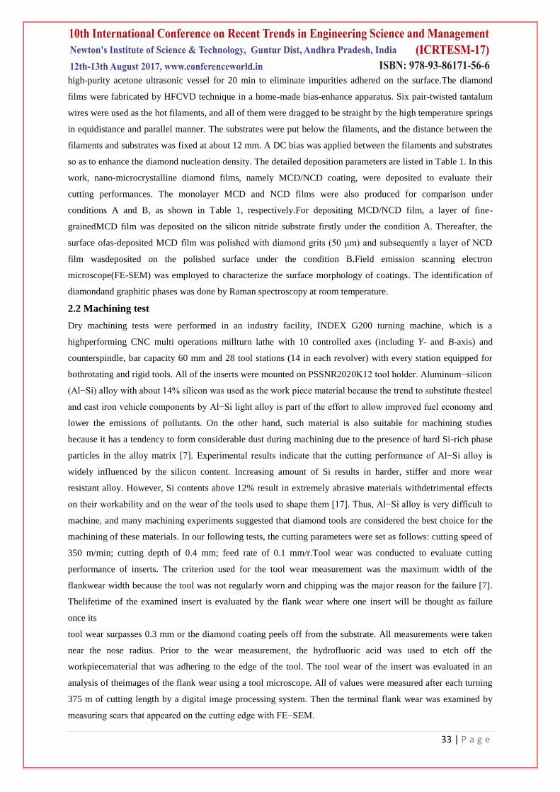
33 | P a g e
high-purity acetone ultrasonic vessel for 20 min to eliminate impurities adhered on the surface.The diamond
films were fabricated by HFCVD technique in a home-made bias-enhance apparatus. Six pair-twisted tantalum
wires were used as the hot filaments, and all of them were dragged to be straight by the high temperature springs
in equidistance and parallel manner. The substrates were put below the filaments, and the distance between the
filaments and substrates was fixed at about 12 mm. A DC bias was applied between the filaments and substrates
so as to enhance the diamond nucleation density. The detailed deposition parameters are listed in Table 1. In this
work, nano-microcrystalline diamond films, namely MCD/NCD coating, were deposited to evaluate their
cutting performances. The monolayer MCD and NCD films were also produced for comparison under
conditions A and B, as shown in Table 1, respectively.For depositing MCD/NCD film, a layer of fine-
grainedMCD film was deposited on the silicon nitride substrate firstly under the condition A. Thereafter, the
surface ofas-deposited MCD film was polished with diamond grits (50 μm) and subsequently a layer of NCD
film wasdeposited on the polished surface under the condition B.Field emission scanning electron
microscope(FE-SEM) was employed to characterize the surface morphology of coatings. The identification of
diamondand graphitic phases was done by Raman spectroscopy at room temperature.
2.2 Machining test
Dry machining tests were performed in an industry facility, INDEX G200 turning machine, which is a
highperforming CNC multi operations millturn lathe with 10 controlled axes (including Y- and B-axis) and
counterspindle, bar capacity 60 mm and 28 tool stations (14 in each revolver) with every station equipped for
bothrotating and rigid tools. All of the inserts were mounted on PSSNR2020K12 tool holder. Aluminum−silicon
(Al−Si) alloy with about 14% silicon was used as the work piece material because the trend to substitute thesteel
and cast iron vehicle components by Al−Si light alloy is part of the effort to allow improved fuel economy and
lower the emissions of pollutants. On the other hand, such material is also suitable for machining studies
because it has a tendency to form considerable dust during machining due to the presence of hard Si-rich phase
particles in the alloy matrix [7]. Experimental results indicate that the cutting performance of Al−Si alloy is
widely influenced by the silicon content. Increasing amount of Si results in harder, stiffer and more wear
resistant alloy. However, Si contents above 12% result in extremely abrasive materials withdetrimental effects
on their workability and on the wear of the tools used to shape them [17]. Thus, Al−Si alloy is very difficult to
machine, and many machining experiments suggested that diamond tools are considered the best choice for the
machining of these materials. In our following tests, the cutting parameters were set as follows: cutting speed of
350 m/min; cutting depth of 0.4 mm; feed rate of 0.1 mm/r.Tool wear was conducted to evaluate cutting
performance of inserts. The criterion used for the tool wear measurement was the maximum width of the
flankwear width because the tool was not regularly worn and chipping was the major reason for the failure [7].
Thelifetime of the examined insert is evaluated by the flank wear where one insert will be thought as failure
once its
tool wear surpasses 0.3 mm or the diamond coating peels off from the substrate. All measurements were taken
near the nose radius. Prior to the wear measurement, the hydrofluoric acid was used to etch off the
workpiecematerial that was adhering to the edge of the tool. The tool wear of the insert was evaluated in an
analysis of theimages of the flank wear using a tool microscope. All of values were measured after each turning
375 m of cutting length by a digital image processing system. Then the terminal flank wear was examined by
measuring scars that appeared on the cutting edge with FE−SEM.

34 | P a g e
Deposition parameters of as- deposited multilayer diamond films
condition Volume
fraction of
acetone /H2/Ar
Pressure /kPa Deposition
temperature /ºc
Filament
temperature /ºc
Bias current /A Duration/h
Condition A
(for MCD
films)
1.6/97.5/0
4-5 800-850 2200±100 3 6
Condition B
(for MCD
films)
3/66/30 1-3 850-900 2200±100 4 5

35 | P a g e
SEM surface images of the samples [W (8μm)/XC85]: before (a)and after annealed during 30 min at 800°C (b),
1000°C (c) and 1100°C (d).
III. RESULTS AND DISCUSSION
3.1 Analysis by X-rays diffraction (XRD)
Figure 1 shows the XRD patterns for the samples. The spectrum of the not-annealed samples shows the
existence of only one phase of W, represented by 3 peaks with 40.6°,73.6° and 115.16°, corresponding to the
plans (110), (211)and (222) respectively. On the other hand the annealing during 30min at 700°C samples does
not make any structural modification compared to the state “not annealed”, where we noted the existence of the
three peaks of W with a texture of the layer according to the direction (222) Fig. 1: XRD spectra of the samples
[W (8μm)/XC85]: before (a) and afterannealed during 30 min at 800°C (b), 1000°C (c) and 1100°C
(d).However, the annealing of 30 min at 1100°C, allows the observation of new peaks with the disappearance of
twopeaks of tungsten W(110) and W(211). These new peaks indicate the formation of two new phases: the
binary phase W2C and ternary Fe3W3C.The annealing of 30 min at a higher temperature, 1100°C,does not
change anything in the composition of samples ,except that it supports the growth of the phases formed
previously (W2C and Fe3W3C).
36 | P a g e
3.2. Study of Surface Morphology
The study of the morphology of the samples by SEM also shows that the surface morphology of samples
angleswith the time and the temperature of annealing. The figure 2 illustrates the images obtained with the
SEM.In the case not-annealed and annealing at 700°C during 30 min (fig. 2.a & b) the surface of the samples is
relatively smooth, but it presents small white particles. After an annealing with 900°C during 30 min (fig. 2.c),
the surface morphology changes with the appearance of the cracks on the surface of the samples W(
8μm)/XC85.The annealing at 1100 ° C for 30 min caused a remarkable increase of the cracks (fig. 2.d). This
may be related to the reaction between the substrate and the thin layers of W
3.3. Micro-Hardness Measurements
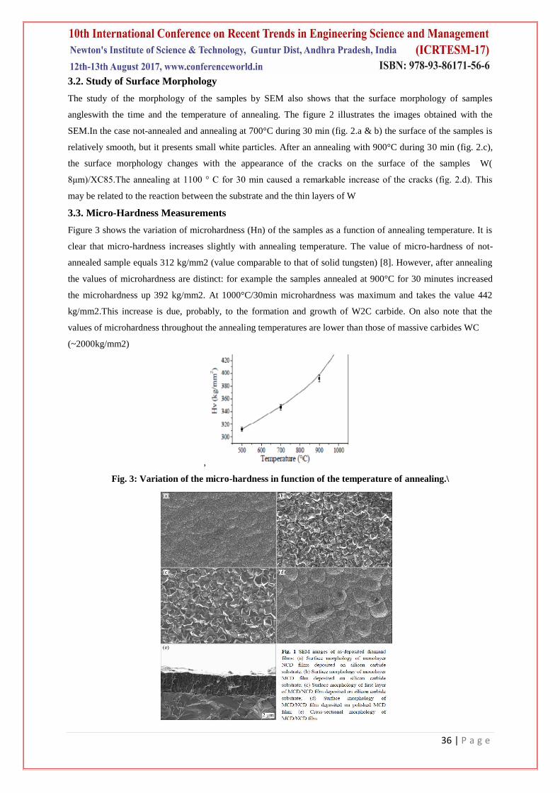
Figure 3 shows the variation of microhardness (Hn) of the samples as a function of annealing temperature. It is
clear that micro-hardness increases slightly with annealing temperature. The value of micro-hardness of not-
annealed sample equals 312 kg/mm2 (value comparable to that of solid tungsten) [8]. However, after annealing
the values of microhardness are distinct: for example the samples annealed at 900°C for 30 minutes increased
the microhardness up 392 kg/mm2. At 1000°C/30min microhardness was maximum and takes the value 442
kg/mm2.This increase is due, probably, to the formation and growth of W2C carbide. On also note that the
values of microhardness throughout the annealing temperatures are lower than those of massive carbides WC
(~2000kg/mm2)
,
Fig. 3: Variation of the micro-hardness in function of the temperature of annealing.\

37 | P a g e
3.1 Characterization of as-Deposited Diamond Films
Figure 1 shows the surface morphologies of as-deposited diamond films. For the monolayer NCD film, the
E−SEM image of its surface (Fig. 1(a)) shows that the substrate is covered by a layer of NCD filmswith
diamond grains in nanometric level. Figure 1(b) shows the surface morphology of the monolayer MCDfilm,
which indicates the typical features of conventional microcrystalline diamond coating with highly facetedgrains
and the columnar structures. For MCD/NCD film,firstly, a layer of MCD film is deposited on the siliconcarbide
insert. This layer of MCD film can facilitate adhesion strength enhancement of deposited multilayerdiamond
films on silicon carbide substrate due to the mechanical interactions between diamond and SiC grainsof
substrate [15]. The surface morphology suggests that the MCD film has a columnar structure, originating from
large diamond grains at the free surface (Fig. 1(c)). These are responsible for the high values of
roughness.Therefore, the as-deposited MCD film was polished with diamond grits in order to produce a flat
surface. Subsequently, a layer of NCD film was deposited on this polished MCD film. Then, the surface
morphology ofas-deposited MCD/NCD film can be seen in Fig. 1(d), which shows that the micron-sized
diamond grains are
completely covered by many nano-sized diamond crystallites. It is clear that MCD and NCD films have avery
distinct kind of structure as grain growth is suppressed by decreasing the atomic H density with theincrement of
partial substitution by Ar, thus increasing the renucleation of diamond [6]. The cross-sectionalSEM image (Fig.
1(e)) indicates a thickness of 12–14 μm for the deposited MCD/NCD film.The quality of as-deposited coatings
was examined by their physical properties by the corresponding Raman signatures. The typical NCD features
present in the Raman spectrum of as-deposited NCD and MCD/NCD films, as presented in Fig. 2. A
significantly broadening peak near 1332 cm−1 can be observed due to the decreasein grain size and phase
purity, which is indicative of sp3diamond. Another peak located at approximately 1560cm−1, which can be
assigned as the G band (1550−1580cm−1) [18,19], is responsible for the contribution fromthe sp2 component.
The presence of scattering intensityat 1560 cm−1 is due to increasing graphite-like sp2bonded components at
the grain boundaries in films. Onthe other hand, the Raman spectrum for the monolayerMCD film shows a sharp
peak located in 1335 cm−1 andno graphitic peaks, which reveals the high purity andexcellent quality of the film.
The shift between the sharppeak and the diamond peak (1332 cm−1) is associatedwith the residual stress of the
MCD film [20].
3.2 Cutting Performance of as-deposited Multilayer
diamond films
Figure 3 shows the flank wear for all the as-deposited diamond coated inserts and uncoated insert as a function
of cutting length. The worn surfaces of uncoated insert, NCD, MCD and MCD/NCD coated inserts are shown in
Figs. 4−7. The corresponding surface morphologies of their cutting edges are also examined by FE−SEM (Fig.
8). The flank wear of the uncoated insert surpasses 0.3 mm after 1875 m of cutting length. An important feature
of the NCD coated insert is the coating peeling during the initial 375 m turning process, as shown in Fig. 5 and
Fig. 8(b). Such phenomena are a result of the higher degree of sp2 content in NCD films because the higher the
graphite content at the interface, the lower the bonding strength to the substrate [21]. It is worth noting that the
MCD crystalline purity is higher compared with NCD grade. In fact, the MCD sample has the smallest non-
diamond phase content and thus its adhesive strength is strengthened. As a result, the MCD film relative to
NCDfilm exhibits a significant enhancement in its cutting performance. Its flank wear shows that MCD

38 | P a g e
coatedinsert can have a life of more than 1500 m of cutting length. However, the failure still occurs after 2250 m
ofcutting length because the diamond coating peels off from the substrate, as shown in Fig. 6(e) and Fig.
8(c).Comparatively, the MCD/NCD coated insert shows a slow increasing tendency in flank wear during
wholeturning process, which suggests that CVD diamond film can protect insert from suffering severe wear due
to itsextremely high hardness and unique wear resistance, and plays a decisive role in prolonging the lifetime of
theinserts. The results show that the MCD/NCD coated insert exhibits very lower flank wear than MCD
coatedinsert and uncoated insert, which may be attributed to the nanocrystalline diamond coating with smooth
surfaceand high wear resistance [6,12]. No coating peeling is NCD film compared with NCD film. On the other
hand,the smoother surface of MCD/NCD film can lead to potential lower friction between the insert and
workpiecematerial, which is beneficial to the chip evacuation and reducing the cutting force. Therefore, the tool
wear ofMCD/NCD coated insert is very low. However, the MCD film has a high surface toughness and thus
increasescutting force. This results in the fact that the MCD coated insert exhibits the coating peeling only after
2250m of cutting length

39 | P a g e
IV. CONCLUSION
According to the results obtained in this study, we can conclude that it is possible to work out hard
tungstencarbide coatings by indirect method consists the coating of a steel substrate, rich in carbon by a layer of
tungsten, then the annealing of together to support the diffusion of carbon and the formation of carbides with
tungsten. The thermal annealing of the samples leads to the formation of the carbide W2C but with a lower
growth rate for the thin layer of thickness 8 μm. The morphology of surface and the micro hardness also
depends on the thicknesses of the thin layers of tungsten. 1) Multilayer diamond films are deposited onsilicon
nitride inserts with a mixture of acetone,hydrogen and argon as the reactant gas by the HFCVDmethod. Double-
layer structure (MCD/NCD) is fabricated initially by the deposition of the rough
microcrystalline diamond layers and then the smooth fine-grained nanocrystalline diamond layers.
Suchmultilayer diamond coatings not only display good adhesion and wear resistant properties, but also

40 | P a g e
havehigh surface smoothness.2) For comparative purpose, the uncoated insert and monolayer NCD and MCD
coated inserts are also adopted in this work. The respective coating structure results in dissimilar cutting
performance in dry turning of Al−Si alloys at 350 m/min of cutting speed, 0.4 mm of cutting depth and 0.1
mm/r of feed. The MCD/NCD coated insert exhibits the prefect behavior as tool wear.
For this coating, the flank wear is very low after turning 3000 m of cutting length and no diamond peeling
occurs. The performance of the monolayer MCD coated insert is slightly inferior due to the high hardness.
Theconventional monolayer NCD film, featured by a cauliflower-like morphology, suffers the coating
peelingfrom its lower adhesion between diamond coating and substrate. 3) Compared with the uncoated inserts,
themultilayer diamond film can protect inserts from suffering severe wear due to its extremely high hardnessand
unique wear resistance, and plays a decisive role in prolonging the lifetime of the inserts.
REFERENCES
[1] R. Koc, S. K. Kodambaka, Journal of the European Ceramic Society20 (2000) 1859.
[2] J. Esteve, E. Martinez, G. Zambrano and P. Prieto, Superficies &Vacio, 9 (1999) 276.
[3] C. Liang1, F. Tian1, Z. Wei1, Q. Xin and Li Can, Nanotechnology,14 (2003) 955.
[4] K.A. Taylor, Thin Solid Films 40 (1977) 189.
[5] E. Eser, R.E. Ogilvie, K.A. Taylor, J. Vac. Sci. Technol. 15(2) (1978)396.
[6] P. Dubcek, N. Radic, O. Milat, S. Bernstorff, Surface and CoatingsTechnology 151/152 (2002) 218.
[7] H.-Y. Yang, X.-A.Zhao, M.-A.Nicolet, Thin Solid Films 158 (1988)45.
[8] H. Romanus, V. Cimalla, J.A. Schaefer, L. Spie, G. Ecke, J. Pezoldt;Thin Solid Films 359 (2000) 146.
[9] G. Keller, R. Erz, I. Barzen, M. Weiler, K. Jung, H. Ehrhardt;Vacuum 41(4/6) (1990)1294.
[10] P. Gouy-Pailler, Y. Pauleau , J. Vac. Sci. Technol. A 11(1) (1993) 96.
[11] N. Radic, B. Grzeta, O. Milat, J. Ivkov, M. Stubicar, Thin Solid Films320 (1998) 192.
[12] P.K. Srivastava, V.D. Vankar, K.L. Chopra, Bull. Mater.Sci. 8(3)(1986) 379.
[13] C. M. Kelly, D. Garg, P.N. Dyer; Thin Solid Films, 219 (1992) 103.
[14] Y. Hatano, M. Takamori, K. Matsuda, S. Ikeno, K. Fujii, K.Watanabe; Journal of Nuclear Materials 307/311 (2002)
1339.

41 | P a g e
[15] H. Weishart, V. Heera, W. Matz, W. Skorupa, Diamond Rel. Mater. 6(1997) 1432.
[16] Pierson, Hugh O., Handbook of Chemical Vapor Deposition (CVD):Principles, Technology, and Applications,
Published in the United States of America by Noyes publications, 1992
[17] Stephen W. H. Yih, Chun T. Wang, “Tungsten: sources, metallurgy,properties, and applications” Plenum Press, New
York ,1979.
[18] KOPF A, FEISTRITZER S, UDIER K. Diamond coated cutting toolsfor machining of non-ferrous metals and fibre
reinforced polymers [J]. International Journal of Refractory Metals & Hard Materials,2006, 24: 354−359.
[19] AMARAL M, OLIVEIRA F J, BELMONTE M, FERNANDES A J S,COSTA F M, SILVA R F. Tailored Si3N4
ceramic substrates for CVD diamond coating [J]. Surface Engineering, 2003, 19: 410−416.
[20] BELMONTE M. Diamond coating of coloured Si3N4 ceramics [J].Diamond and Related Materials, 2005, 14: 54−59.
[20] XU Feng, ZUO Dun-wen, LU Wen-zhuang, ZHU Yong-wei, WANG Min. Grid and substrate bias effects on
mechanical properties ofdiamond films prepared by HFCVD [J]. Transactions of Nonferrous Metals Society of China,
2009, 19: s722−s726.
[21] CABRAL G, REIS P, TITUS E, MADALENO J C, DAVIM J P,GRACIO J, AHMED W, JACKSON M J. Impact of
surfaceroughness of diamond coatings on the cutting performance when drymachining of graphite [J]. International
Journal of Manufacturing Technology and Management, 2008, 15: 121−152.
[22] ALMEIDA F A, AMARAL M, OLIVEIRA F J, SILVA R F.Machining behaviour of silicon nitride tools coated with
micro-,submicro- and nanometric HFCVD diamond crystallite sizes [J].Diamond and Related Materials, 2006, 15:
2029−2034.
[23] ARUMUGAM P U, MALSHE A P, BATZER S A. Dry machining ofaluminum−silicon alloy using polished CVD
diamond-coated cutting tools inserts [J]. Surface & Coatings Technology, 2006, 200:3399−3403.
[24] QIN F, HU J, CHOU Y K, THOMPSON R G. Delamination wear of nano-diamond coated cutting tools in composite
machining [J]. Wear,2009, 267: 991−995.
[24] ALMEIDA F A, SACRAMENTO J, OLIVEIRA F J, SILVA R F.Micro- and nano-crystalline CVD diamond coated
tools in the turning of EDM graphite [J]. Surface & Coatings Technology, 2008,203: 271−276.
[25] HU J, CHOU Y K, THOMPSON R G. Nanocrystalline diamondcoating tools for machining high-strength Al alloys [J].
International Journal of Refractory Metals & Hard Materials, 2008, 26: 135−144.
[26] HU J, CHOU Y K, THOMPSON R G, BURGESS J, STREET S.Characterizations of nano-crystalline diamond coating
cutting tools [J]. Surface & Coatings Technology, 2007, 202: 1113−1117.
[27] LIANG Q, VOHRA Y K, THOMPSON R. High speed continuousand interrupted dry turning of A390
aluminum/silicon alloy using nanostructured diamond coated WC-6 wt.% cobalt tool inserts byMPCVD [J]. Diamond
and Related Materials, 2008, 17: 2041−2047.
[28] ALMEIDA F A, AMARAL M, OLIVEIRA F J, FERNANDES A J S,SILVA R F. Nano to micrometric HFCVD
diamond adhesion strength to Si3N4 [J]. Vacuum, 2007, 81: 1443−1447.
[29] SHEN B, SUN F H. Deposition and friction properties ofultra-smooth composite diamond films on Co-cemented
tungsten carbide substrates [J]. Diamond and Related Materials, 2009, 18:238−243.
[30] SUN F H, ZHANG Z M, CHEN M, SHEN H S. Improvement ofNai-chao CHEN, et al/Trans. Nonferrous Met. Soc.
China 23(2013) 1985−1992adhesive strength and surface roughness of diamond films onCo-cemented tungsten carbide
tools [J]. Diamond and Related Materials, 2003, 12: 711−718.
[31] SUN F H, MA Y P, SHEN B, ZHANG Z M, CHEN M. Fabricationand application of nano-microcrystalline composite
diamond films on the interior hole surfaces of Co cemented tungsten carbidesubstrates [J]. Diamond and Related
Materials, 2009, 18: 276−282.
42 | P a g e
[32] CASTRO G, ALMEIDA F A, OLIVEIRA F J, FERNANDES A J S,SACRAMENTO J, SILVA R F. Dry machining of
silicon−aluminium alloys with CVD diamond brazed and directly coated Si3N4 ceramictools [J]. Vacuum, 2008, 82:
1407−1410.
[33] PRAWER S, NEMANICH R J. Raman spectroscopy of diamond anddoped diamond [J]. Philosophical Transactions of
the Royal Society of London Series A: Mathematical Physical and EngineeringSciences, 2004, 362: 2537−2565.
[34] ROY D, BARBER Z H, CLYNE T W. Ag nanoparticle inducedsurface enhanced Raman spectroscopy of chemical
vapor deposition diamond thin films prepared by hot filament chemical vapour deposition [J]. Journal of Applied
Physics, 2002, 91: 6085−6088.
[35] FERREIRA N G, ABRAMOF E, CORAT E J, TRAVA-AIROLDI V J.Residual stresses and crystalline quality of
heavily boron-doped diamond films analysed by micro-Raman spectroscopy and X-raydiffraction [J]. Carbon, 2003, 41:
1301−1308.
[36] MALLIKA K, KOMANDURI R. Low pressure microwave plasmaassisted chemical vapor deposition (MPCVD) of
diamond coatings on silicon nitride cutting tools [J]. Thin Solid Films, 2001, 396:145−165.
[37] NESLADEK M, VANDIERENDONCK K, QUAEYHAEGENS C,KERKHOFS M, STALS L M. Adhesion of
diamond coatings on cemented carbides [J]. Thin Solid Films, 1995, 270: 184−188.
Associate Professor with HOD & Research scholar in -VTU, Department of Mechanical
Engineering, Newtons institute of science and technology College,Guntur,AP, India


![MICROCRYSTALLINE WAX - ::krishna::krishna.nic.in/PDFfiles/MSME/Chemical/MICROCRYSTALLINE WAX[1].pdf · Specification of Microcrystalline wax ... MRF Ltd. 1.000 43372 ... The content](https://img.pdfslide.net/doc/110x75/5aa76b097f8b9ac5648c1342/microcrystalline-wax-krishna-wax1pdfspecification-of-microcrystalline-wax.jpg)