Embed Size (px)
Citation preview
2012 International ESD Workshop
Page 1
Study of Voltage-Step Dependency on the TLP-Measured Secondary
Breakdown Current (It2) of ESD Clamp Circuit in a 16V Double-Diffused Drain
MOS (DDDMOS) Process Chia-Tsen Dai1, Po-Yen Chiu1, Ming-Dou Ker1, Fu-Yi Tsai2,
Yan-Hua Pan2, and Chia-Ku Tsai2 1 Institute of Electronics, National Chiao-Tung University, Hsinchu, Taiwan
2 Faraday Technology Corporation, Hsinchu, Taiwan
Biography
Page 2 2012 International ESD Workshop
The presenter, Po-Yen Chiu, is currently a Ph.D. candidate at Institute of Electronics, National Chiao-Tung University, Hsinchu, Taiwan. His current research interests include ESD protection design for CMOS integrated circuits, mixed-voltage I/O interface circuits, and analog circuit design.
Abstract
Page 3 2012 International ESD Workshop
The measured results of Transmission-Line Pulse System (TLP) in the traditional RC-based ESD clamp circuit have different secondary breakdown current levels (It2) when using different voltage steps.
In order to get a reasonable TLP It2 result, the voltage-step dependency should be taken into consideration, especially in high-voltage CMOS processes.
Outline
Page 4 2012 International ESD Workshop
Introduction Implementation of ESD Clamp Circuit in a 162-nm 16-V
DDDMOS Process Experimental Results Failure Analysis Conclusions
Page 5 2012 International ESD Workshop
Introduction (1/1)
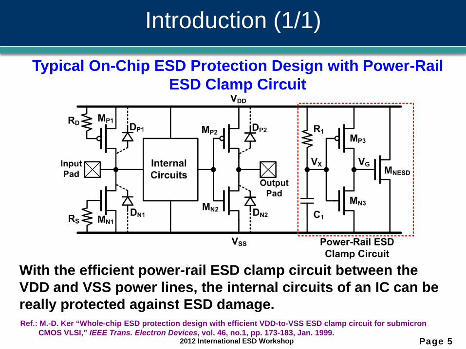
Typical On-Chip ESD Protection Design with Power-Rail ESD Clamp Circuit
With the efficient power-rail ESD clamp circuit between the VDD and VSS power lines, the internal circuits of an IC can be really protected against ESD damage. Ref.: M.-D. Ker “Whole-chip ESD protection design with efficient VDD-to-VSS ESD clamp circuit for submicron
CMOS VLSI,” IEEE Trans. Electron Devices, vol. 46, no.1, pp. 173-183, Jan. 1999.
Page 6 2012 International ESD Workshop
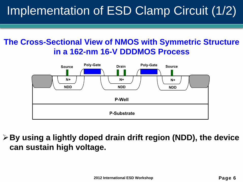
Implementation of ESD Clamp Circuit (1/2)
The Cross-Sectional View of NMOS with Symmetric Structure in a 162-nm 16-V DDDMOS Process
By using a lightly doped drain drift region (NDD), the device can sustain high voltage.
Page 7 2012 International ESD Workshop
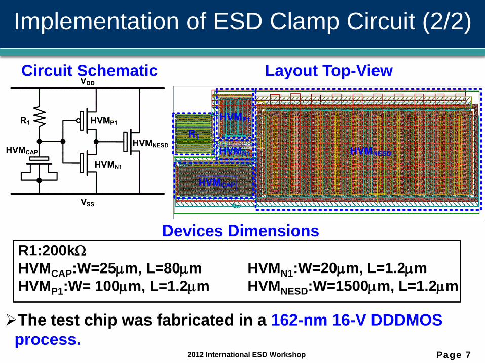
Implementation of ESD Clamp Circuit (2/2)
Circuit Schematic Layout Top-View
R1:200kΩ HVMCAP:W=25µm, L=80µm HVMP1:W= 100µm, L=1.2µm
Devices Dimensions
HVMN1:W=20µm, L=1.2µm HVMNESD:W=1500µm, L=1.2µm
The test chip was fabricated in a 162-nm 16-V DDDMOS process.
Page 8 2012 International ESD Workshop
Experimental Results (1/3)
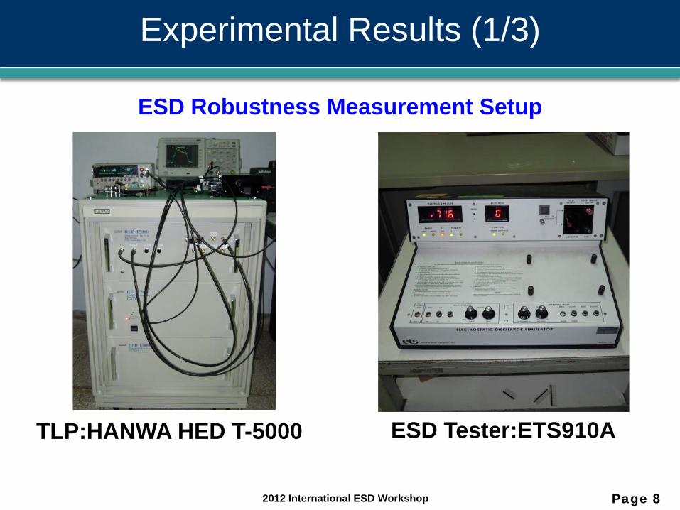
ESD Robustness Measurement Setup
ESD Tester:ETS910A TLP:HANWA HED T-5000
Page 9 2012 International ESD Workshop
Experimental Results (2/3)
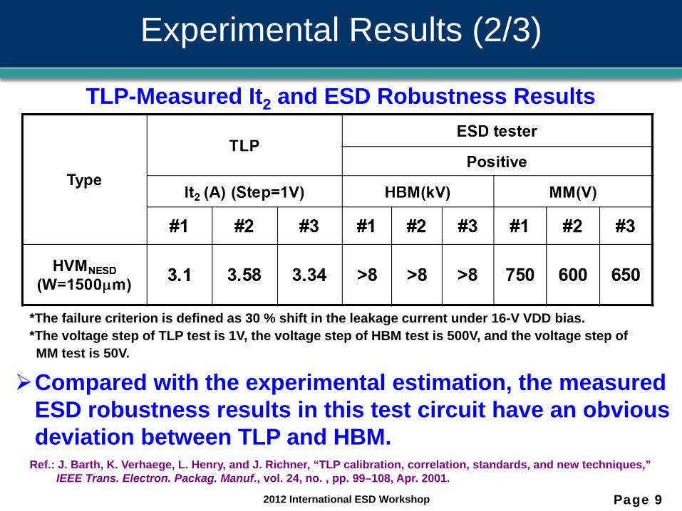
TLP-Measured It2 and ESD Robustness Results
*The failure criterion is defined as 30 % shift in the leakage current under 16-V VDD bias. *The voltage step of TLP test is 1V, the voltage step of HBM test is 500V, and the voltage step of MM test is 50V.
Compared with the experimental estimation, the measured ESD robustness results in this test circuit have an obvious deviation between TLP and HBM.
Ref.: J. Barth, K. Verhaege, L. Henry, and J. Richner, “TLP calibration, correlation, standards, and new techniques,” IEEE Trans. Electron. Packag. Manuf., vol. 24, no. , pp. 99–108, Apr. 2001.
Page 10 2012 International ESD Workshop
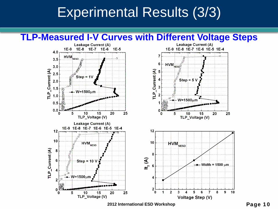
Experimental Results (3/3)
TLP-Measured I-V Curves with Different Voltage Steps
Page 11 2012 International ESD Workshop
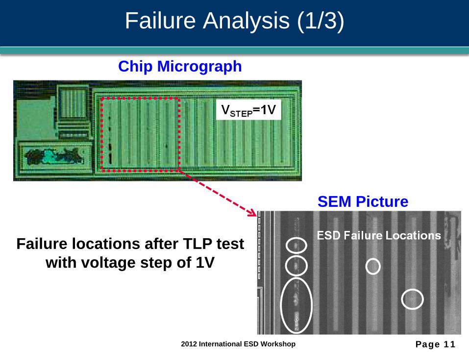
Failure Analysis (1/3)
Chip Micrograph
SEM Picture
Failure locations after TLP test with voltage step of 1V
Page 12 2012 International ESD Workshop
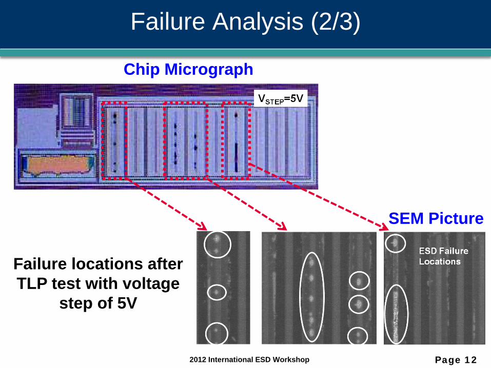
Failure Analysis (2/3)
Chip Micrograph
SEM Picture
Failure locations after TLP test with voltage
step of 5V
Page 13 2012 International ESD Workshop
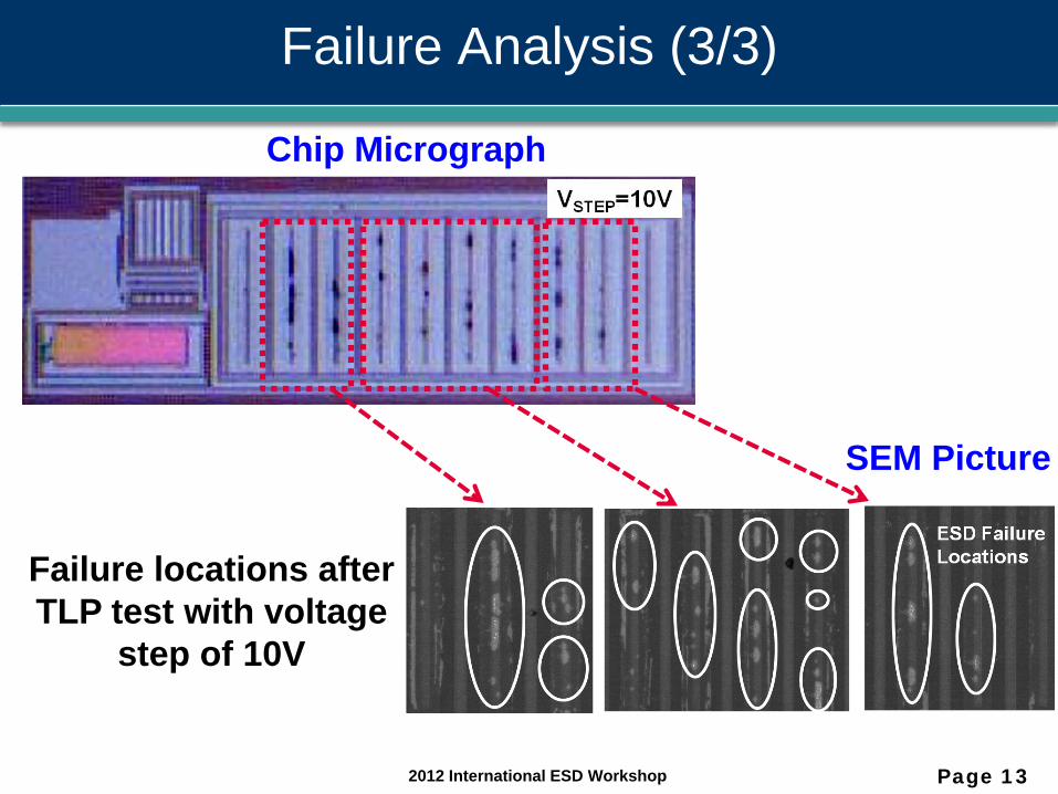
Chip Micrograph
SEM Picture
Failure Analysis (3/3)
Failure locations after TLP test with voltage
step of 10V
Page 14 2012 International ESD Workshop
Discussions (1/2)
All failure locations are located at HVMNESD. However, with different voltage steps in TLP tests, the failure locations and situations are quite different. With a voltage step of 1V, the failure locations are
mainly located at the edge of HVMNESD. Besides, this condition has the worst TLP It2. However, with the voltage step is increased, the circuit
could obtain better TLP It2 in TLP test. Moreover, the failure locations indicates that the HVMNESD can have better turn-on uniformity when the step is larger.
Page 15 2012 International ESD Workshop
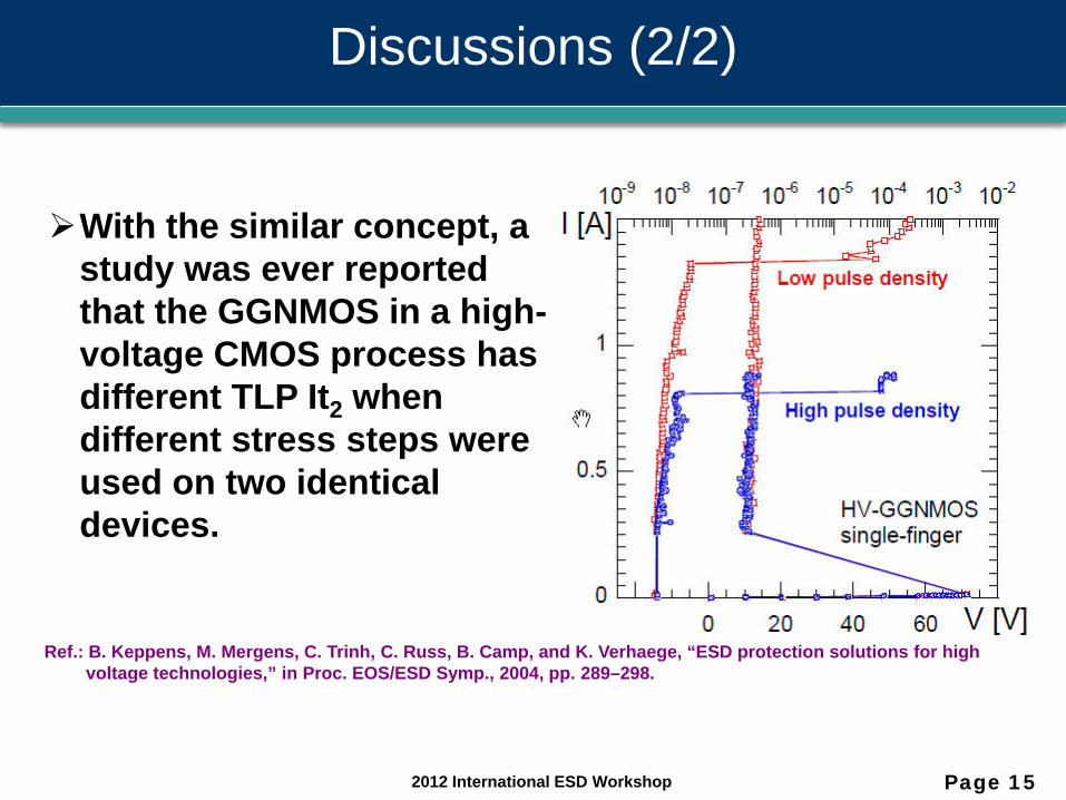
Discussions (2/2)
With the similar concept, a study was ever reported that the GGNMOS in a high-voltage CMOS process has different TLP It2 when different stress steps were used on two identical devices.
Ref.: B. Keppens, M. Mergens, C. Trinh, C. Russ, B. Camp, and K. Verhaege, “ESD protection solutions for high voltage technologies,” in Proc. EOS/ESD Symp., 2004, pp. 289–298.
Conclusions
Page 16 2012 International ESD Workshop
From the measured results of TLP tests, the reason to cause a deviation between TLP test and HBM test has been found. With different cumulative energy caused by different
voltage steps in TLP test, different TLP It2 is found. Therefore, in order to get the credible and reasonable result for TLP It2, the voltage-step dependency should be taken into consideration especially in high-voltage CMOS processes. Moreover, the real physical mechanisms to cause the It2
variation also need to be further studied.
References
Page 17 2012 International ESD Workshop
M.-D. Ker, "Whole-chip ESD protection design with efficient VDD-to-VSS ESD clamp circuit for submicron CMOS VLSI," IEEE Trans. Electron Devices, vol. 46, no.1, pp. 173-183, Jan. 1999.
A. Amerasekera, L. v. Roozendaal, J. Abderhalden, J. Bruines, and L. Sevat, “An analysis of low voltage ESD damage in advanced CMOS processes,” in Proc. EOS/ESD Symp., vol. EOS-12, 1990, pp. 143–150.
A. Amerasekera and C. Duvvury, “The impact of technology scaling onESD robustness and protection circuit design,” in Proc. EOS/ESD Symp., 1994, pp. 237–245.
J. Barth, K. Verhaege, L. Henry, and J. Richner, “TLP calibration, correlation, standards, and new techniques,” IEEE Trans. Electron. Packag. Manuf., vol. 24, no. , pp. 99–108, Apr. 2001.
B. Keppens, M. Mergens, C. Trinh, C. Russ, B. Camp, and K. Verhaege, “ESD protection solutions for high voltage technologies,” in Proc. EOS/ESD Symp., 2004, pp. 289–298.