Embed Size (px)
Citation preview

STUDYING THE FABRICATION OF THIN FILM SILICON
SOLAR CELL ON POLYMERIC AND GLASS SUBSTRATE
ANG PUN CHONG
UNIVERSITI SAINS MALAYSIA
2016

STUDYING THE FABRICATION OF THIN FILM SILICON
SOLAR CELL ON POLYMERIC AND GLASS SUBSTRATE
by
ANG PUN CHONG
Thesis submitted in fulfillment of the requirements for the degree of
Master of Science
May 2016

ii
ACKNOWLEDGEMENT
Firstly, I would like to express my sincere gratitude to my main supervisor,
Professor Kamarulazizi Ibrahim for his valuable guidance and continuous support
throughout the course of this project. Besides of guidance and support, your financial
assistance from Grant 203/PSF/6721001 is much appreciated.
Thanks to Universiti Sains Malaysia (USM) for giving me this chance to
complete my master. Furthermore, technical supports from Nano-Optoelectronics
Research and Technology Laboratory (N.O.R) staffs; Mr. Anas, Ms. Ee Bee Choo,
Mr. Hazhar Hassan, Mr. Abdul Jamil Yusuf, Mr. Yushamdan and Mr. Aswafi are
gratefully acknowledged. Also thanks to my fellow friends; Mohd. Zamir, Ooi Poh
Kok, Chai Ying Qi and others (not mentioned here) who have given me useful advices
throughout this research.
Finally, I would like to thank my family members for supporting me during the
whole research. Not to forget thanks to my girlfriend, Cheng Wei Leng for constant
motivation and patience throughout this research and thesis writing process.

iii
TABLE OF CONTENTS
Page
Acknowledgement ii
Table of Contents iii
List of Tables vii
List of Figures viii
List of Abbreviations xiii
List of Symbols xv
Abstrak xvi
Abstract xviii
CHAPTER 1 - INTRODUCTION
1.1 Photovoltaics Technologies 1
1.2 Problem Statement 3
1.3 Scope of Research 5
1.4 Research Originality 6
1.5 Objectives of Research 6
1.6 Thesis Outline 7
CHAPTER 2 – LITERATURE REVIEW
2.1 Introduction 8
2.2 Thin Film Solar Cells 8
2.3 Issues of Thin Film Si Solar Cells Research 9
iv
2.4 Progress in Thin Film Silicon Solar Cells Research (Methods and 10
Approaches)
CHAPTER 3 – THEORY
3.1 Introduction 17
3.2 Solar Spectrum 17
3.3 Properties of Silicon Material 18
3.4 Doping of Silicon 19
3.5 Absorption Coefficient of Silicon 21
3.6 PN Junction and PIN Junction Formation 23
3.7 Equivalent Circuit of a Solar Cell 25
3.8 Dark and Light Current-Voltage Characteristic 26
CHAPTER 4 – MATERIALS AND METHODS
4.1 Introduction 29
4.2 Equipment for Thin Film Depositions 29
4.2.1 Electron Beam (E-beam) Evaporation 29
4.2.2 Thermal Evaporation 32
4.2.3 Magnetron Sputtering 33
4.3 Annealing Equipment 34
4.4 Equipment for Thin Film Characterizations 35
4.4.1 Structural Properties 35
4.4.1 (a) Energy Dispersive X-Ray (EDX) Spectroscopy 35
4.4.1 (b) High Resolution X-Ray Diffractometer (HR-XRD) 37
4.4.1 (c) Raman Spectroscopy 38
4.4.2 Surface Morphologies 39

v
4.4.2 (a) Atomic Force Microscopy (AFM) 39
4.4.3 Electrical Properties 40
4.4.3 (a) 4-Point Probe Meter 40
4.4.3 (b) Hall-Effect Measurement System 41
4.4.3 (c) Solar Simulator System 42
4.4.4 Optical Properties 43
4.4.4 (a) Ultraviolet – Visible (UV-Vis) Spectrophotometer 43
4.5 Thin Film Silicon Solar Cells Fabrication and Characterizations 44
4.5.1 Thin Film Silicon Solar Cells on PET Substrate 44
4.5.2 Thin Film Silicon Solar Cells on PI and Glass Substrate 47
CHAPTER 5 – RESULTS AND DISCUSSIONS
5.1 Introduction 50
5.2 Properties of Substrate 50
5.3 Fabrication of Thin Film Silicon Solar Cell on PET Substrate 55
5.3.1 Aluminum Thin Films by Thermal Evaporation 55
5.3.2 Aluminum-Silicon Alloy Thin Films by E-beam Co-evaporation 62
5.3.3 Antimony-Silicon Alloy Thin Films by E-beam Co-evaporation 68
5.3.4 Properties of Thin Film Silicon Solar Cell on PET Substrate 74
5.3.5 Disadvantages of Thin Film Silicon Solar Cell on PET Substrate 76
and Its Solutions.
5.4 Fabrication of Thin Film Silicon Solar Cell on Sodalime Glass and 78
PI Substrate
5.4.1 Tungsten Thin Films by Magnetron Sputtering 78
5.4.2 Aluminum-doped Silicon Thin Films on Glass and PI Substrate 83
by AIC Technique

vi
5.4.3 Epitaxial Thickening of Intrinsic Si Thin film on Crystallize 96
Si Seed Layer
5.4.4 Gallium Doped Zinc Oxide Thin Film by Magnetron 98
Sputtering
5.4.5 Properties of Thin Film Silicon Solar Cell on Sodalime Glass 100
and PI Substrate
5.5 Summary 104
CHAPTER 6 – CONCLUSIONS AND RECOMMENDATIONS
6.1 Conclusions 105
6.2 Recommendations 106
REFERENCES 107
PUBLICATIONS 113

vii
LIST OF TABLES
Page
Table 2.1 Details of parameters for EVA solar cell fabrication 13
Table 2.2 Typical parameter for an ALICE and ALICIA cells 14
Table 5.1 Deposition parameters and thickness for Al thin films on 55
PET substrates
Table 5.2 Al peak detected, FWHM and crystal size of the evaporated 58
samples
Table 5.3 Al to Si weight ratio for the samples 62
Table 5.4 Results of the Hall effect measurement for Al-Si alloy 65
thin film on PET
Table 5.5 Sb to Si weight ratio of the samples 68
Table 5.6 Electrical properties of the Sb-Si alloy thin film by Hall effect 71
measurement
Table 5.7 Parameters of device performance for Si thin film solar cell on 76
PET substrate
Table 5.8 Results of the XRD pattern and calculated crystal size for 81
the samples
Table 5.9 Sheet resistance and Resistivity of W thin film on glass and 82
PI substrate
Table 5.10 Process parameters of the SF6/Ar plasma etching 84
Table 5.11 Peak position and the FWHM value for each sample 88
Table 5.12 Hall effect results for crystallize Si thin film on PI substrate 95
Table 5.13 Results of Hall effect measurement for Ga doped ZnO thin film 100
on glass and PI substrate
Table 5.14 Parameters of device performance for Si thin film solar cell on 103
glass and PI substrate

viii
LIST OF FIGURES
Page
Figure 1.1 Efficiency and cost projections for first, second and third 3
generation photovoltaic technology
Figure 1.2 Overall PV market shares in year 2010 (divide into different 4
technology)
Figure 2.1 Process steps of EVA, ALICE and ALICIA solar cell 11
Figure 2.2 Schematic structure of the EVA solar cell 12
Figure 2.3 Cross section TEM image of an ALICIA cell 14
Figure 2.4 Photo of line-focus laser crystallization technique attached 15
with TEM image
Figure 2.5 Schematic drawing of IMEC’s Si thin film solar cell 16
Figure 3.1 Spectral irradiance of sun under AM 1.5 Global 17
Figure 3.2 Schematic of (a) p-type doped and (b) n-type doped Si crystal 20
lattice
Figure 3.3 Schematic for the positon of EF level for (a) intrinsic, (b) p-type 20
doped and (c) n-type doped Si
Figure 3.4 Plot of absorption coefficient (α, in logarithmic scale) of 21
various semiconductor materials at 300 K versus wavelength (nm)
Figure 3.5 Band structure of direct and indirect band gap material 22
Figure 3.6 (a) Schematic diagram of a PN junction (b) Band diagram of a 23
PN junction
Figure 3.7 (a) Schematic diagram of a PIN junction (b) Band diagram of a 24
PIN junction
Figure 3.8 Equivalent circuit of a solar cell 25
Figure 3.9 Dark and light current-voltage characteristic for solar cell 26
Figure 3.10 Light I-V curve in positive current position 27
ix
Figure 4.1 E-beam evaporation system 30
Figure 4.2 Schematic diagram of e-beam evaporation system 30
Figure 4.3 Thermal evaporation system 32
Figure 4.4 Magnetron sputtering system 33
Figure 4.5 Annealing furnace 35
Figure 4.6 EDX spectroscopy system integrated to field emission scanning 36
electron microscope (FESEM)
Figure 4.7 HR-XRD system 37
Figure 4.8 Raman spectroscopy system 38
Figure 4.9 AFM system 39
Figure 4.10 4-point probe meter 40
Figure 4.11 Hall-effect measurement system 41
Figure 4.12 Solar simulator system 42
Figure 4.13 UV-Vis Spectrophotometer 43
Figure 4.14 Basic process flow of thin film Si solar cell fabrication on 44
PET substrate
Figure 4.15 Metal mask for Ag fingers and busbar coating 46
Figure 4.16 Schematic diagram for Si thin film solar cell on PET substrate 46
(picture was not drawn in scale)
Figure 4.17 Basic process flow of thin film Si solar cells fabrication on 47
glass and PI substrate
Figure 4.18 Schematic diagram for Si thin film solar cell on glass or PI 49
substrate (picture was not drawn in scale)
Figure 5.1 EDX spectra for PET, PI and sodalime glass 51
Figure 5.2 XRD pattern for (a) PET, (b) PI and (c) sodalime glass 52
Figure 5.3 AFM result (Planar and 3D) for PET, PI and sodalime glass 53
Figure 5.4 Transmittance of PET, PI and sodalime glass substrates 54

x
Figure 5.5 EDX spectra of Al thin film on PET substrate 55
(Thickness = 440nm)
Figure 5.6 FESEM image of the Al thin films on PET substrate 56
Figure 5.7 XRD patterns of the as-evaporated films on PET substrate 57
Figure 5.8 AFM images (spot size 5 μm x 5 μm) of the as-evaporated Al 58
thin films on PET substrate
Figure 5.9 Sheet resistances of the Al thin films on PET substrate with 59
different thickness
Figure 5.10 Surface reflectance curve range 300 nm – 1200 nm for the 61
samples on PET substrate
Figure 5.11 EDX mapping of Al-Si alloy thin film on PET substrate 63
(Al/Si ratio = 0.5%)
Figure 5.12 EDX spectra for Al-Si alloy thin film on PET substrate 63
(Al/Si ratio = 0.5%)
Figure 5.13 XRD pattern for Al-Si alloy thin film on PET 64
(Al/Si ratio = 0.5%)
Figure 5.14 (a) Resistivity (b) hole mobility (c) doping concentration against 65
Al/Si ratio of the Al-Si alloy thin film on PET
Figure 5.15 Transmission, reflection and absorption of Al-Si alloy thin film 67
(Doping concentration = 1.57×10¹⁶ atoms/cm3)
Figure 5.16 EDX mapping result for Sb-Si alloy thin film (Sb/Si weight 69
ratio = 0.5 %)
Figure 5.17 EDX spectra for Sb-Si alloy thin film on PET (Sb/Si weight 69
ratio = 0.5 %)
Figure 5.18 XRD pattern of Sb-Si alloy thin film on PET (Sb/Si weight 73 70
ratio = 0.5 %)
Figure 5.19 (a) Resistivity (b) electron mobility (c) doping concentration 71
against Sb/Si ratio of the Sb-Si alloy thin film on PET
Figure 5.20 (a) Transmission, reflection and absorption curves of Sb- 73
Si alloy thin films
Figure 5.21 Schematic structure of Si thin film solar cell on PET substrate 74
Figure 5.22 Illuminated and dark IV curve for Si thin film solar cell on PET 75
substrate

xi
Figure 5.23 FESEM image for W thin film on (a) glass and (b) PI substrate 79
Figure 5.24 EDX spectra for W thin film on (a) glass and (b) PI substrate 79
Figure 5.25 XRD pattern of W thin film on glass and PI substrate 80
Figure 5.26 AFM images for sputtered W thin film on (a) glass and 81
(b) PI substrate
Figure 5.27 Reflection of W thin film on glass and PI substrate 83
Figure 5.28 The schematic diagram (not drawn to scale) and the cross section 85
FESEM image of the sample during AIC process
Figure 5.29 (a) Planar FESEM images of the samples after Al removal. 86
(b) Larger magnification of planar FESEM image for the sample
with SF6/Ar plasma etching (40 sec)
Figure 5.30 Raman spectra of the samples 87
Figure 5.31 XRD pattern of the sample with SF6/Ar plasma etch for 20 s 89
Figure 5.32 (a) Sheet resistance (b) Mobility and (c) Doping concentration 90
of the samples with different duration of SF6/Ar plasma etching
Figure 5.33 Optical transmission curves of the samples with different 91
duration of SF6/Ar plasma etching
Figure 5.34 Raman spectra for crystallize Si thin film on PI substrate (Raman 93
spectra for the same film on glass substrate was included for
comparison purpose)
Figure 5.35 XRD pattern of crystallize Si thin film on PI substrate 94
Figure 5.36 Raman spectra of intrinsic Si thin film on crystallize seed layer 96
(both glass and PI substrate)
Figure 5.37 XRD pattern of intrinsic Si thin film on crystallize seed layer 97
(both glass and PI substrate)
Figure 5.38 XRD pattern of sputtered Ga doped ZnO thin film on glass and 99
PI substrate
Figure 5.39 Si thin film solar cell on (a) glass and (b) PI substrate 101
Figure 5.40 FESEM cross section image for Si thin film solar cell on glass 101
substrate

xii
Figure 5.41 Schematic structure of Si thin film solar cell on glass or PI 102
substrate
Figure 5.42 Illuminated IV curve for Si thin film solar cell on glass and PI 103
substrate

xiii
LIST OF ABBREVIATIONS
AFM Atomic Force Microscopy
AIC Aluminum Induced Crystallization
AM Air mass
ARC Anti-reflection coating
a-Si Amorphous silicon
ASTM American Society for Testing and Materials
BSR Back surface reflector
CB Conduction band
CIS Copper indium diselenide
CIGS Copper indium gallium diselenide
cost/Wattp Cost per watt peak
c-Si Monocrystalline silicon
CZ Czochralski
CZTS Copper zinc tin sulfide
DC Direct current
DI Deionized
DRA Diffuse reflectance accessories
E-beam Electron beam
EDX Energy Dispersive X-Ray
Eg Band gap
ESRL Earth System Research Laboratory
eV Electron volt
FESEM Field emission scanning electron microscope
FWHM Full width half maximum
FZ Float Zone
GW Gigawatts
HR-XRD High Resolution X-Ray Diffractometer
ICDD International Centre for Diffraction Data
IMEC Interuniversity Microelectronics Centre
IRENA International Renewable Energy Agency
I-V Current voltage
LED Light emitted diode
LPC Liquid phase crystallization
mc-Si Multicrystalline silicon
MFC Mass flow controller
MG-Si Metallurgical-grade silicon
MHz Megahertz
NCDC National Climate Data Center
PET Polyethylene terephathalate
PI Polyimide
PL Photoluminescence
Ppm Parts per millions
PV Photovoltaics

xiv
PVD Physical vapor deposition
RF Radio frequency
RIE Reactive ion etching
RMS Root mean square
SIMS Secondary Ion Mass Spectroscopy
SoG-Si Solar-grade silicon
SPC Solid phase crystallization
STC Standard test condition
TEM Transmission Electron Microscope
TWh Terawatts hour
UMG-Si Upgraded metallurgical-grade silicon
UNSW University of New South Wales
USD Dollar America
UV-Vis Ultraviolet to visible
VB Valence band
xv
LIST OF SYMBOLS
A Area of device
A Absorption
β Full width half maximum (FWHM) in radians
c Speed of light
D Crystal size
E Energy of photons
FF Fill factor
h Planck’s constant
Impp Maximum current
Isc Short circuit current
Jsc Short circuit current density
k Constant value of 0.94
λ Wavelength
η Conversion efficiency
Pin Total illuminated power
Pmpp Maximum power
R Reflection
Rs Series resistance
Rsh Shunt resistance
T Transmission
θ Bragg’s angle
Vmpp Maximum voltage
Voc Open circuit voltage

xvi
MENGKAJI FABRIKASI FILEM NIPIS SILIKON SEL SURIA DI
ATAS SUBSTRAT POLIMER DAN KACA
ABSTRAK
Filem nipis silikon sel suria atas PET substrat difabrikasi dengan
mendepositkan filem nipis aluminium (Al) (440nm) sebagai penyambung belakang,
filem nipis Al-Si aloi (1 µm) sebagai penyerap, filenm nipis Sb-Si alloy (120nm)
sebagai pemancar dan perak (Ag) sebagai penyambung hadapan. Penukaran
kecekapan untuk filem nipis silikon sel suria atas PET ialah sekitar 0.105 %.
Kecekapan yang rendah ini disebabkan oleh sifat amorfus lapisan penyerap dan
pemancar. Untuk mengatasi isu ini, teknik penghabluran aluminium teraruh (AIC)
digunakan untuk mencipta filem nipis hablur silikon. Teknik AIC perlu memanaskan
sampel sekurang-kurangnya 400 °C, oleh itu PET yang melebur sekitar 250 °C tidak
sesuai digunakan sebagai substrat. Substrat PET digantikan dengan substrat kaca dan
PI. Struktur untuk filem nipis silicon sel suria di atas kaca dan PI adalah filem nipis
tungsten (W) (500 nm) sebagai penyambung belakang, filem nipis Si didopkan dengan
Al (ketebalan 180 nm dengan teknik AIC) sebagai lapisan seed dan back surface field
(BSF), penebalan epitalesi intrinsik silikon (i-Si) sebagai penyerap, filem nipis zink
oksida (ZnO) didopkan dengan galium (Ga) sebagai pemancar dan Ag penyambung
hadapan. Filem nipis hablur silikon berjaya dicipta dengan teknik AIC (didopkan
secara semula jadi dengan Al dengan kepekatan pendopan sekitar 1019 atom/cm3) di
atas substrat kaca dan PI. Keputusan Raman menunjukkan bahawa mereka adalah
bersifat hablur dengan puncak Raman (kaca: 520 cm- 1, PI: 518 cm- 1) iaitu berhampiran
puncak Raman c-Si (521 cm- 1). Keputusan XRD menunjukkan meraka adalah dalam
fasa hablur Si (111). Penebalan epitalesi lapisan biji ini untuk mencipta hablur i-Si

xvii
sebagai penyerap juga berjaya dilakukan. Tetapi, qualiti hablur untuk lapisan i-Si
adalah sedikit buruk berbanding dengan lapisan biji. Filem nipis ZnO didopkan dengan
Ga juga menunjukkan sifat hablur dengan fasa hablur ZnO (002) (mempunyai
kepekatan pendopan sekitar 1020 atom/cm3), sifat ini adalah sesuai untuk menjadikan
sebagai lapisan pemancar. Penukaran kecekapan untuk filem nipis sel suria di atas
substrat kaca dan PI adalah 1.034 % dan 0.924 %.

xviii
STUDYING THE FABRICATION OF THIN FILM SILICON
SOLAR CELL ON POLYMERIC AND GLASS SUBSTRATE
ABSTRACT
Si thin film solar cell on PET substrate was fabricated by depositing Aluminum
(Al) thin film (440 nm) as back contact, Al-Si alloy thin film (1 µm) as absorber layer,
Sb-Si allloy thin film (120 nm) as emitter and Silver (Ag) front contact. The final
conversion efficiency of the Si thin film solar cell on PET is around 0.105 %. The low
efficiency of this device was believed to be cause by the amorphous nature of absorber
and emitter layer. In order to solve this issue, fabrication of crystalline Si thin film by
Aluminum Induced Crystallization (AIC) technique and SF6/Ar plasma etch methods
were implemented. AIC technique needed to anneal the sample at least to 400 °C,
therefore PET which melts at around 250 °C is not suitable. PET substrate was replaced
by glass and PI. The structure of Si thin film solar cell for both glass and PI substrate
are tungsten (W) thin film (500 nm) as back contact, Al doped Si thin film (180 nm by
AIC) as seed layer and back surface field (BSF), epitaxial thickening intrinsic Si (i-Si)
as absorber, gallium (Ga) doped zinc oxide (ZnO) thin film as emitter and Ag front
contact. Crystallize Si thin film by AIC technique (with naturally Al doped of
concentration about 1019 atoms/cm3) was successfully fabricated on both glass and PI
substrate. Raman results shows that the sample are crystalline nature with Raman
peaks (Glass: 520 cm-1, PI: 518 cm-1) close to Raman peak for c-Si (521 cm-1). XRD
spectra shows they are in Si (111) crystalline phase. Epitaxial thickening of this seed
layer to create a crystallize i-Si absorber layer is successfully done. However the
crystalline quality of i-Si layer is slightly worst compare to seed layer. Sputtered Ga
doped ZnO thin film also shown a crystalline nature with ZnO (002) crystalline phase

xix
with doping concentration of around 1020 atoms/cm3, which is suitable for emitter layer.
The final conversion efficiency of Si thin film solar cell on glass and PI increased to
1.034 % and 0.924 %.

1
CHAPTER 1
INTRODUCTION
1.1 Photovoltaics Technologies
Photovoltaics technologies are classified into three major categories, which are:
1) first generation monocrystalline (c-Si) and multicrystalline (mc-Si) wafer-based Si
solar cells; 2) second generation thin film based solar cells; 3) third generation high
efficiency thin film solar cells.
Nowadays most of the commercial solar cells in the market are based on silicon
wafer, which are described as first generation technology. The first generation c-Si and
mc-Si wafer-based solar cells exhibit high efficiency (17 - 22%). However, the
manufacturing costs for these types of solar cells are relatively high. The high
manufacturing cost was due to the high purity c-Si and mc-Si wafers which was
produced by Czochralski (CZ), Float Zone (FZ) and casting or directional
solidification processes (Mahajan and Harsha, 1999). The current module costs for the
first generation solar cells is less than USD$ 1.4/Watt. (IRENA, 2013). The lowest
limit of the costs of this generation was predicted to be as low as USD$ 1/Watt (Green,
2003).
The second generation solar cells were based on thin film technology which
were deposited on foreign substrates such as glass, plastic and metal sheet. This
technology generally includes three major families, which are: 1) thin film Silicon-
based such as amorphous silicon (a-Si) and multicrystalline silicon (mc-Si); 2)
cadmium telluride (CdTe); 3) copper indium diselenide (CIS), copper indium gallium
diselenide (CIGS) and copper zinc tin sulfide (CZTS). Si thin films based solar cells

2
have more advantages compared to other family due to its stability, manufacturability
and abundance. Si thin films based solar cells can avoid resource availability issue
which was related to Te and In (Green, 2009). Furthermore, Si is the most abundant
element in earth crust after Oxygen (O2) gas (Green, 2006). The conversion efficiency
for second generation solar cells are around 5 to 15%, which is lower compared to Si
wafer-based solar cells However, the lower efficiency can be compensated by using
the low cost substrate, such as glass and plastic. The overall costs of second generation
cells is 2 to 3 times lowers than the cells manufactured from the first generation (Green,
2003).
The third generation solar cells are based on the advanced thin films concepts.
Third generation solar cells are not constrained by the efficiency limit of first and
second generation, which is 31% under non-concentrated sunlight (Green, 1994). The
expected efficiency limit of this generation is as high as 74 % under non-concentrated
sunlight (Farrell and Ekins-Daukes, 2011). With the high efficiency conversion, the
final cost of third generation cells is 2 to 3 times lower than that of second generation
cells. The most common type of third generation cell is tandem cell. Tandem cell is
the solar cell produced by combination of several solar cells with different band gaps
onto one another to become a complete single cell. Besides tandem cell, hot carrier
cell, thermophotovoltaic conversion and multiple quantum well solar cells are also
classified as the third generation cells (Green, 2001).
Figure 1.1 shows the possible production costs per unit area and the energy
conversion efficiency ranges for the three generations of photovoltaics technologies.
First generation solar cells are classified as the group of high production costs and
moderate efficiency. With the conversion efficiency of around 20 %, the production
cost of this generation in the market is around US$ 150/m2. Second generation thin

3
films technology has much lower production cost (US$ 30/m2) but even more modest
efficiency (5 to 12 %). Third generation technology offers at least 2 to 3 times higher
efficiency than second generation with almost the same production cost.
Figure 1.1: Efficiency and cost projections for first, second and third generation
photovoltaic technology (Green, 2001).
1.2 Problem Statement
Si is still the preferable material for solar cells fabrication due to its abundance,
non-toxicity, good electronic properties and proven reliability (Green, 2000).
Furthermore, Si has an optical band gap of 1.12 eV, which is close to the band gap of
an ideal photoconverter (1.4 eV) (Nelson, 2003). Owing to these advantages,
crystalline Si (c-Si and mc-Si) based solar cells still dominate around 87% of the PV
market. Figure 1.2 shows the overall PV market shares in year 2010, which is divided
into different technologies (EPIA, 2010).

4
Figure 1.2: Overall PV market shares in year 2010 (divide into different technology).
The main disadvantage for crystalline Si based solar cells is its high
manufacturing cost. Low impurity (impurity concentration < 1ppb) and high quality in
term of crystal perfection of mono-crystalline Si (c-Si) produced by Czochralski (CZ)
and Float-Zone (FZ) techniques prove to yield high efficiency Si solar cells. However,
these growth techniques must go through multiple purification steps which make this
type of crystalline Si very expensive. Besides of mono-crystalline Si, there is a type of
crystalline Si produced via casting and directional solidification technique. This type
of crystalline Si called multi-crystalline Si (mc-Si). Production of mc-Si involves
lower cost and higher throughput compared to c-Si. Crystalline Si based solar cells
produce from mc-Si wafer prove to have around 80 % performance of c-Si wafer based
solar cell.
Besides, both of c-Si and mc-Si based solar cells are also highly material-
intensive. In order to make sure a complete absorption of incident sunlight, the
thickness of the crystalline Si (both c-Si and mc-Si) wafers are fabricated to around
87%
6%
5%2%
Crystalline Si
CdTe
Thin film Si
CIS/CIGS

5
180 to 200 µm. The needs of such high thickness was due to the indirect band gap
properties of Si material. This indirect band gap property causes it to be a poor light
absorption material (Runyan, 1965). Furthermore, owing to the high cost of raw silicon
material, which occupies around 50% of the finished PV module (Rubin, 2010), the
production cost of the crystalline Si wafer based solar cells in the market is still high
(around USD 2 to 3/Wattp) for large scale manufacturers (Green, 2003).
1.3 Scope of Research
This work will focus on the study of the second generation solar cells. As
discussed on the previous section, second generation solar cell is the technology which
involves the deposition of thin film semiconductor on the foreign substrate. In this
experiment, thin film Si solar cell will be deposited on the foreign substrates via
electron beam evaporation method. This is an effective way to reduce the cost/Wattp
of the final solar cells because of the low material consumption.
To reduce material consumption, the thickness of the Si thin film will reduce
to 1 – 1.5 µm (150 to 200 times thinner than the thickness of the conventional Si wafer)
(Song, 2005). In addition, the cost/Wattp of the final product can be reduced further by
replacing the conventional glass substrate to polymeric type substrate (such as
polyethylene terephthalate, PET and polyimide, PI). The cost of polymeric substrate is
lower compared to glass substrate, therefore the cost/ Wattp of the final products can
be reduced. Besides, polymeric is also light in weight and highly flexible. These
properties make it capable for roll to roll deposition process (Rath et al., 2008).
Electron beam evaporation is chosen to be the main deposition method of thin film Si
due to its high deposition rate (up to 1 µm/min).

6
The advantages of low material consumption and low cost polymeric substrate
could potentially yield to lower cost/Wattp thin film Si solar cells with reasonable
device conversion efficiency.
1.4 Research Originality
Originality of this research is the fabrication of low cost second generation thin
film Si solar cell on flexible polymeric and glass substrate. Low cost can be achieved
by much lower material consumption due to thinner structure (150 to 200 times thinner
compared to conventional Si wafer based cell). The fabrication method consists e-
beam deposition, Aluminum Induced Crystallization (AIC) and Sulfur Hexafluride
(SF6)/Argon (Ar) plasma etch. This fabrication method is rarely reported in literature.
In this research, a function crystalline thin film Si solar cell on polymeric and glass
substrate can be fabricated at low temperature (400 °C), which leads to the advantage
of low energy consumption during the fabrication processes.
1.5 Objectives of Research
The objectives of this work are listed as below:
1. Study the fabrication of thin film Si solar cells on polyethylene
terephathalate (PET) substrates via electron beam evaporation.
2. Study the fabrication of thin film Si solar cells on sodalime glass and
polyimide (PI) substrates via electron beam evaporation and Aluminum
Induced Crystallization (AIC) technique.
3. To compare the performance between the thin film Si solar cells deposited
on PET, sodalime glass and PI substrate.

7
This work does not aim to fabricate high efficiency thin film Si solar cells on
PET, sodalime glass and PI substrates, but rather to understand the underlying factors
which affect the performance of the devices.
1.6 Thesis Outline
Chapter 1 explains the solar energy, photovoltaics technologies and problem
statement. Scope and objectives of this research are also discussed in this chapter.
Chapter 2 briefly goes through the thin film solar cells. Discussed issues and
approach in thin film Si solar cell research.
Chapter 3 presents basic of relevant theories such as solar spectrum, properties
of Si, doping of Si, PN junction, PIN junction, Current-Voltage characteristic and
efficiency calculation.
Chapter 4 presents the material and methods needed for the fabrication of thin
film Si solar cell on polymeric and glass substrate. This includes the deposition
equipment, annealing equipment and several types of characterization equipment.
Besides, the detail of fabrication process steps for Si thin film solar cell on polymeric
and glass substrate will be explained.
Chapter 5 illustrates the experimental results, calculations, explains and
discuss the observations and finding.
Chapter 6 summarizes the overall findings and lists some recommendations
for future works on thin film Si solar cell fabrication on polymeric and glass substrate.

8
CHAPTER 2
LITERATURE REVIEW
2.1 Introduction
This chapter will go through the basic of thin film solar cells and the types of
thin film solar cells technologies. Besides, the thin film solar cells issues, such as weak
absorption of Si and high recombination at defects will also be studied. Finally, the
progress of thin film solar cells researches by Photovoltaics Centre of Excellence,
University of New South Wales (UNSW) and Interuniversity Microelectronics Centre
(IMEC) will be shown in this chapter.
2.2 Thin Film Solar Cells
Thin film solar cells or the second generation solar cells which fabrication is
performed by depositing multiple layers or thin films of photovoltaic material onto a
foreign substrate. The material of the substrate can be stainless steels, glasses or
flexible plastic materials. Currently, there are few types of thin film technologies, such
as amorphous silicon (a-Si), microcrystalline silicon (µc-Si), polycrystalline silicon
(pc-Si), cadmium telluride (CdTe), copper indium diselenide (CIS), copper indium
gallium diselenide (CIGS), copper zinc tin sulfide (CZTS) and polymer based solar
cells (Shah et al., 2004). The thin film solar cells are typically deposited via chemical
vapour deposition (CVD), physical vapour deposition (PVD), electrochemical and
spin-on methods onto a foreign substrate. The substrate is used to improve the
mechanical strengths. Thin film solar cells have advantage of fairly high optical
absorption (especially for CdTe and CIGS), however, its minority carrier diffusion

9
lengths is fairly low due to the presence of defects and grain boundaries. Normally,
thin film solar cells have low conversion efficiencies (5 – 15%) but with two to three
times lower production costs compared to the first generation cells (Nelson, 2003).
2.3 Issues of Thin Film Si Solar Cells Research
Thin film Si solar cell technology believes to be one of the effective approaches
which leads to the reduction of the total manufacturing cost of solar cells. However,
there are several issues that need to be solved.
The main issue is the weak light absorption material of Si (especially at near
infrared region) at low thickness. It is due to the fact that Si is an indirect band gap
semiconductor (Brendel, 2005). In order to solve this problem, light trapping strategy
is applied within the structure of thin film solar cells. The advantage of light trapping
strategy is to increase optical path length of photon within the solar cell which leads to
higher potential of photon absorption and directly increases the photocurrent
generation (Cho et al., 2011). Besides, the light trapping strategy can be improved by
incorporating of several thin film deposition, such as anti-reflection coating (ARC)
(usually SixNy, ZnO, SiO2 or ITO) (Yang et al., 2011). Furthermore, deposition of a
back surface reflector (BSR) layer at the back surface of solar cells is also an effective
approach to trap more photons. There are several types of BSR, they are metal,
dielectric or multilayer porous or a silver (Ag) plasmonics nanostructures (Sai et al.,
2009, Pillai and Green, 2010).
High recombination of electron-hole pairs at defects is another issue that need
to be solved. There are several types of defects in Si thin film, they are lattice mismatch,
grains boundaries and dangling bonds. These types of defects will act as effective trap
states and recombination centres to electron-hole pairs (Mahajan and Harsha, 1999).

10
Normally, the defects are created due to contamination of impurities into Si atoms
during deposition of Si thin film. Besides, defects can also be created by structural
imperfection within the Si thin film which is generated during deposition.
The issue of high recombination at defects can be solved by depositing the thin
film Si in a high vacuum environment. One of the high vacuum deposition methods is
e-beam evaporation. Typically, the base pressure of e-beam evaporation chamber can
go up to > 10 -8 Torr and deposition pressure of > 10 -7 Torr. E-beam evaporation is
simple and attractive due to its high deposition rate (up to 1 µm/min) (Kunz et al.,
2009). In additions, high temperature deposition process or low temperature deposition
process with further treatment of high annealing temperature to produce large grains
absorber and defects annealing are also the methods to solve this issue (Rau et al.,
2009). Recently, liquid phase crystallization (LPC) is proved to be able to produce a
high quality crystalline Si thin film on glass. These types of Si thin films have low
defect density, high carrier motilities, and high minority carrier lifetime of over 260 ns
(Varlamov et al., 2013).
2.4 Progress in Thin Film Silicon Solar Cells Research (Methods and
Approaches)
There are two main groups of researchers have done extensive research in thin
film Si solar cells. They are Photovoltaics Centre of Excellence, University of New
South Wales (UNSW) and Interuniversity Microelectronics Centre (IMEC).
Researchers in UNSW focuses on the study of pc-Si thin film solar cells on
borosilicate glass. Three different types of pc-Si thin film solar cells have been
developed, which are EVA, ALICE and ALICIA (Aberle, 2006b). Figure 2.1 shows
the process steps of EVA, ALICE and ALICIA.
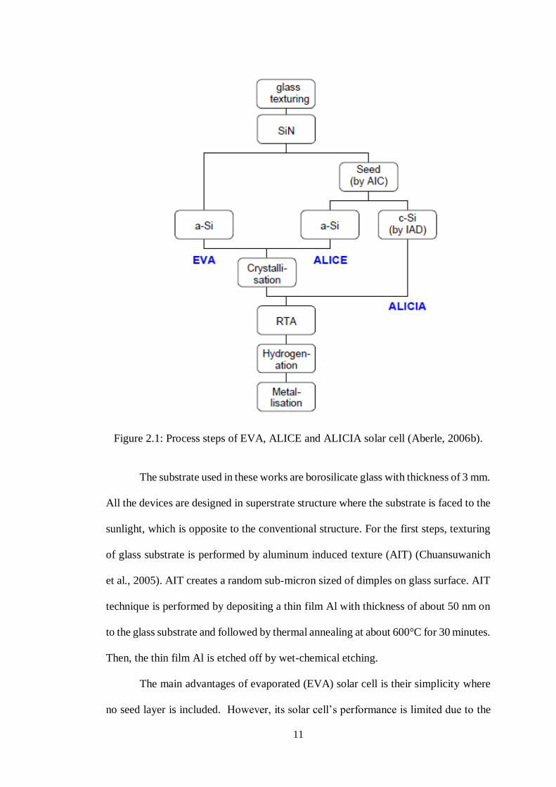
11
Figure 2.1: Process steps of EVA, ALICE and ALICIA solar cell (Aberle, 2006b).
The substrate used in these works are borosilicate glass with thickness of 3 mm.
All the devices are designed in superstrate structure where the substrate is faced to the
sunlight, which is opposite to the conventional structure. For the first steps, texturing
of glass substrate is performed by aluminum induced texture (AIT) (Chuansuwanich
et al., 2005). AIT creates a random sub-micron sized of dimples on glass surface. AIT
technique is performed by depositing a thin film Al with thickness of about 50 nm on
to the glass substrate and followed by thermal annealing at about 600°C for 30 minutes.
Then, the thin film Al is etched off by wet-chemical etching.
The main advantages of evaporated (EVA) solar cell is their simplicity where
no seed layer is included. However, its solar cell’s performance is limited due to the

12
relatively small grain size (normally in range of 1 – 2 µm), which affects its electrical
performance caused by the grain boundaries effects. EVA Si thin film solar cell on
borosilicate glass substrate with conversion efficiency of 4 % is successfully fabricated
(Kunz et al., 2008). The schematic structure of the EVA solar cell is shown as Figure
2.2.
Figure 2.2: Schematic structure of the EVA solar cell (Kunz et al., 2008).
An antireflection coating (ARC) of Silicon Nitride (SiN) layer was firstly
deposited onto the borosilicate glass substrate. The ARC layer serves as both
antireflection coating and barrier layer for contaminations from substrate. ARC layer
can be deposited by plasma enhanced chemical vapor deposition (PECVD) or
sputtering. After that, the combination layers of a-Si thin film emitter, absorber and
back surface field (BSF) layer are deposited by electron beam (e-beam) evaporation
under high vacuum (base pressure around 2 × 10⁻⁸ Torr; working pressure around 2 ×
10-7 Torr). The total thickness of these three layers are controlled within around 2 µm.
Then, the sample will go through solid phase crystallization (SPC) and rapid thermal
annealing (RTA). After RTA process, the sample was exposed to hydrogen plasma
treatment. The details of parameters for EVA solar cell fabrication is shown in Table
2.1.

13
Table 2.1: Details of parameters for EVA solar cell fabrication (Kunz et al., 2008).
For ALICE and ALICIA solar cell, both of them are fabricated by deposition
of epitaxial thickening of Si absorber layer on Aluminum Induced Crystallization (AIC)
seed layer. The seed layer is formed by thermally annealed a-Si and Al bilayers at
500 °C. The epitaxial thickening layer of ALICE cells is deposited by e-beam
evaporation followed with SPC process (or called Solid Phase Epitaxy, SPE)
(Widenborg et al., 2005), which is the same process as EVA cell. For ALICIA cell, the
epitaxial thickening layer is deposited by Ion Assisted Deposition (IAD) (Aberle et al.,
2005).
Table 2.2 shows the typical parameter for an ALICE and ALICIA cells. The
emitter layer of around 150 nm with doping concentration of nearly 1 × 1019 cm-3 is
fabricated by AIC technique. AIC technique proved that a well crystalline Si thin film
can be fabricated by stacking a-Si layer with Al layer and annealed below the eutectic
temperature (577 °C) (Nast et al., 1998, Nast et al., 2001).

14
Table 2.2: Typical parameter for an ALICE and ALICIA cells (Aberle, 2006b).
Figure 2.3 shows the cross section TEM image of an ALICIA cell. The figure
illustrates a good transfer of crystalline quality from seed layer produced by AIC to
the epitaxial thickening absorber layer.
Figure 2.3: Cross section TEM image of an ALICIA cell (Varlamov et al., 2013).
Besides of the SPC and AIC crystallization technique, UNSW research team
members have invented a new crystallization technique called liquid phase
crystallization (LPC) technique. This technique proved to have Si thin film with grain
size up to millimeter (mm) scale. The highest conversion efficiency of Si thin film
solar cell achieved by LPC technique is 11.7 % (Varlamov et al., 2013). LPC of Si thin
film is performed by line-focus laser crystallization. Figure 2.4 shows the photo of

15
line-focus laser crystallization technique, the resulting grain size is shown in TEM
image (attached in Figure 2.4).
Figure 2.4: Photo of line-focus laser crystallization technique attached with TEM
image (Varlamov et al., 2013).
IMEC research team has also done a massive research in Si thin film solar cells
fabricated by AIC seed layer concepts. Si thin film solar cell on alumina substrate with
the efficiency of 4.5% was achieved by them using AIC seed layer concept with
epitaxial thickening of absorber layer (Gordon et al., 2005). The seed layer is
fabricated by depositing a bi-layer of a-Si and Al thin film (200 nm and 230 nm
respectively) onto an alumina substrate using e-beam evaporation. After deposition,
the samples are annealed in tube furnace with temperature at 500 °C (under N2 ambient
for 0.5 to 3 hours). The top Al layer is then removed by Al selective etchants. Si
epitaxial thickening layer is deposited on the seed layer by commercial single-wafer
epitaxial reactor (ASM Epsilon 2000) using trichlorosilane diluted in H2 at 1130 °C
(under atmospheric pressure). The in situ boron (B) doping is performed by adding the
flow of diborane gas (Gordon et al., 2005).
IMEC research team successfully fabricated Si thin film solar cell on alumina
substrate with conversion efficiency of 8.0 %. The cell is also fabricated by means of

16
AIC seed layer with epitaxial thickening absorber layer. There is an addition of
improvement step which is the plasma texturing of absorber layer with hexaflurosilane
(SiF6) and nitrous oxide (N2O) gases (Gordon, et al., 2007). Figure 2.5 shows the
schematic drawing of IMEC’s Si thin film solar cell.
Figure 2.5: Schematic drawing of IMEC’s Si thin film solar cell (Gordon, et al.,
2007).
Fabrication of Si thin film solar cell via e-beam evaporation and AIC technique
on low cost polymeric substrate and lower grade sodalime glass are hardly reported in
the literature. One of the reasons is due to its relatively low quality of crystalline Si. In
this research, a-Si thin film solar cell is fabricated on low cost polyethylene
terephthalate (PET) substrate via e-beam co-evaporation technique. In additions, the
structure is improved by fabrication of crystallize Si thin film solar cells on polyimide
(PI) and sodalime glass substrate by means of AIC technique with epitaxial thickening
of absorber layer.

17
CHAPTER 3
THEORY
3.1 Introduction
This chapter will go through a brief introduction of solar spectrum (AM 1.5
Global) and properties of silicon material which included doping of silicon and
absorption coefficient of silicon. The basic formation of PN and PIN junction will also
be studied in this chapter. Lastly, the electrical characteristic of solar cells such as
equivalent circuit and current-voltage characteristic of solar cells will be shown.
3.2 Solar Spectrum
Figure 3.1 shows the solar irradiance (Air Mass, AM 1.5 Global) of sun range
from wavelength of 200 nm to 2500 nm (from ASTM G173-03 reference spectral)
(ASTM, 2008). This is the spectral for terrestrial use, which has an integrated power
of 1000 W/m2.
Figure 3.1: Spectral irradiance of sun under AM 1.5 Global (Nelson, 2003).

18
Air Mass (AM) shows the optical path length of sunlight which need to pass
through before it reaches the surface of earth. AM value determined the total reduction
of sunlight’s power as it pass through the atmosphere. The power reduction is due to
the absorption by air and dust. The AM value is calculated by AM = 1/cos (φ), where
φ is the angle from the vertical line (zenith angle). For AM 1.5, the φ angle is equal to
48.2°. AM 1.5 Global is the standard test condition (STC) for solar cell’s current-
voltage (I-V) characterizations (Nelson, 2003).
3.3 Properties of Silicon Material
Silicon is a semiconductor material with chemical symbol Si and atomic
number 14 (electronic configuration: 2, 8, 4). It is a group IV element in periodic table
with 4 valence electrons. Si is a solid material under room temperature with relatively
high melting point (1414 °C) and boiling point (3265 °C). It crystallizes in a diamond
cubic crystal structure with lattice spacing of 0.5431 nm. Crystalline Si has a gray
metallic color and very brittle.
Si is chosen as the main material for solar cells fabrication due to its abundance,
non-toxicity, proven durability and good electronic properties (Green, 1995). Si is the
most abundant element in earth crust beside Oxygen, O2. There is about 25 % of silica
can be found in earth crust. Besides, Si has a band gap (Eg) of 1.12 eV at room
temperature, which is close to the ideal band gap of a photocenverter (around 1.4 eV)
(Nelson, 2003).
For Si material, the valence band (VB) and conduction band (CB) are separated
by a forbidden gap called band gap (Eg) of 1.12 eV. Electrons are tightly bond and not
freely to move in VB, in order to move freely it must be excited to CB. In Si material,

19
minimum energy required to excite an electron from VB to CB is 1.12 eV (Eg for Si).
Photons which carry the energy of around 1.12 eV can be calculate by formula below,
E = hc/λ
where,
E = Energy of photons in electron volts (eV)
h = Planck’s constant, 4.1357 x 10⁻¹⁵ eV.s
c = Speed of light, 3 x 10⁸ m/s
λ = wavelength of light in nm
From the formula above, photons of wavelength about 1100 nm carry energy
of around 1.12 eV. Therefore, Si needed to absorb photons with wavelength of 1100
nm and below to create free electrons and produce photocurrent.
3.4 Doping of Silicon
Doping of silicon is a technique of introducing selected impurities into pure
(intrinsic) silicon for the purpose of modify its electrical properties. There are two
types of doped Si, which are p-type Si and n-type Si. Doping of Si results one less
electron (hole) known as p-type Si.
Introducing group 3 element (tetravalent atom) such as boron (B) or aluminum
(Al) results extra of holes as the majority carriers in Si which called a p-type doped Si.
For n-type doped Si, group 5 element (pentavalent atoms) such as phosphorus (P),
antimony (Sb) and arsenic (As) need to introduce in to intrinsic Si lattice which
produces extra of electrons as the majority carriers in Si lattice. Figure 3.2 shows the
schematic of p-type and n-type doped Si crystal lattice.

20
Figure 3.2: Schematic of (a) p-type doped and (b) n-type doped Si crystal lattice
(Honsberg and Bowden, 2010).
The Fermi energy (EF) level in an intrinsic Si will shifted due to doping. For
intrinsic Si, EF level is approximately in the middle of valence band (VB) and
conduction band (CB) or half of band gap (Eg/2). On the other hand, the EF level for
p-type doped Si is shift towards VB edge. However, EF level for n-type doped Si is
shift towards CB edge. The schematic for the positon of EF level for intrinsic, p-type
doped and n-type doped Si are shown in Figure 3.3.
Figure 3.3: Schematic for the positon of EF level for (a) intrinsic, (b) p-type doped
and (c) n-type doped Si (Nelson, 2003).

21
3.5 Absorption Coefficient of Silicon
Figure 3.4 shows the plot of absorption coefficient (α, in logarithmic scale) of
various semiconductor materials at temperature of 300 K versus wavelength (nm).
Absorption coefficient measures how far distance into a particular material that light
of a particular wavelength can penetrate before it is absorbed. Material with high
absorption coefficient absorb the light stronger compared to material with low
absorption coefficient.
Figure 3.4: Plot of absorption coefficient (α, in logarithmic scale) of various
semiconductor materials at 300 K versus wavelength (nm) (Honsberg and Bowden,
2010).
From Figure 3.4, it can be seen that all semiconductor material have a sharp
transition edges at their respective band gaps. This phenomenon was due to the photons
with energy lower than the band gap (Eph < Eg) do not have sufficient energy to excite
an electron from valence band to conduction band.

22
In additions, Figure 3.4 shows that Si has a slower transition in its absorption
profile compared to other material like GaAs, CdTe, CdS, InP and a-Si. This is due to
Si is an indirect material while GaAs, CdTe, CdS, InP and a-Si are direct band gap
materials. Direct band gap materials generally have higher ability in optical absorption
compared to indirect band gap material (Nelson, 2003). An indirect band gap material
(i.e. Si) requires assistance from phonons with the right momentum (k) to enable
electron transition from valence band (VB) to conduction band (CB), therefore its
optical absorption is weaker compared to material with direct band gap. Comparison
in band structure of direct and indirect band gap material is shown in Figure 3.5.
Figure 3.5: Band structure of direct and indirect band gap material (Nelson, 2003).

23
3.6 PN Junction and PIN Junction Formation
Figure 3.6 shows the schematic diagram and energy band diagram for a PN
junction. PN junction is formed by joining p-type doped Si with n-type doped Si. P-
type region has high holes concentration while n-type region has high electrons
concentration. When both of these material joining together, holes from p-type region
will diffuse to n-type region and electrons from n-type region will diffuse p-type region
due to concentration gradient at the junction. However, the diffusion process is altered
by formation of an internal electric field. This internal electric field is formed when
the electrons and holes move to the other side of the junction, they leave behind
exposed charges (negative charge on p-type region and positive charge on n-type
region).
Figure 3.6: (a) Schematic diagram of a PN junction (b) Band diagram of a PN
junction (Nelson, 2003).
The PN junction is the core structure for a solar cell devices. PN junction serves
as a barrier to majority carriers and low resistance path for minority carriers. The main
function of the PN junction is to drive the collection of minority carriers which are

24
photogenerated throughout p-type and n-type region to reach junction via diffusion
and drift (Nelson, 2003).
Figure 3.7 shows the schematic diagram and energy band diagram for a PIN
junction. PIN junction is formed where an intrinsic (undoped) Si layer is sandwiched
between p-type doped and n-type doped Si layer. The internal electric field is formed
at the junction or between the p-type doped and n-type doped layer, but the region is
extends wider due to the inclusion of intrinsic layer (Green, 1982).
Figure 3.7: (a) Schematic diagram of a PIN junction (b) Band diagram of a PIN
junction (Nelson, 2003).
This structure is not preferred for thin film solar cells fabrication due to its
imperfect lattice formation resulting from various deposition technique. This lattice
imperfection directly causes the decreases of minority carrier diffusion length. For PIN
structure, p-type and n-type doped layer is generally not contribute to the
photogenerated current. Carriers are mainly generated within the intrinsic layer and
drive towards the p-type and n-type doped layer by the internal electric field (Nelson,
2003).