Embed Size (px)
Citation preview
Substrate aberration and correction formeta-lens imaging: an analytical approachBENEDIKT GROEVER,1 CHARLES ROQUES-CARMES,1,2 STEVEN J. BYRNES,3 AND FEDERICO CAPASSO1,*1Harvard John A. Paulson School of Engineering and Applied Sciences, Harvard University, Cambridge, Massachusetts 02138, USA2Research Laboratory of Electronics, Massachusetts Institute of Technology, Cambridge, Massachusetts 02139, USA3Charles Stark Draper Laboratory, Cambridge, Massachusetts 02139, USA*Corresponding author: [email protected]
Received 25 January 2018; revised 11 March 2018; accepted 12 March 2018; posted 13 March 2018 (Doc. ID 318972); published 12 April 2018
Meta-lenses based on flat optics enabled a fundamental shift in lens production—providing an easier manufac-turing process with an increase in lens profile precision and a reduction in size and weight. Here we present ananalytical approach to correct spherical aberrations caused by light propagation through the substrate by adding asubstrate-corrected phase profile, which differs from the original hyperbolic one. A meta-lens encoding the newphase profile would yield diffraction-limited focusing and an increase of up to 0.3 of its numerical aperturewithout changing the radius or focal length. In tightly focused laser spot applications such as direct laserlithography and laser printing, a substrate-corrected meta-lens can reduce the spatial footprint of themeta-lens. © 2018 Optical Society of America
OCIS codes: (050.1965) Diffractive lenses; (050.5080) Phase shift; (050.6624) Subwavelength structures.
https://doi.org/10.1364/AO.57.002973
1. INTRODUCTION
In recent years, metasurfaces have emerged as a new way tocontrol light through the optical properties of sub-wavelengthelements patterned on the flat surface of a substrate. Asub-wavelength element can locally change the amplitude,polarization, and phase of an incident electromagnetic waveto realize various optical functions in a compact configuration[1–6]. A metasurface can be produced through a single lithog-raphy step of nanofabrication, which can be scaled easily tohigh-output manufacturing processes.
One of the most promising applications of metasurfaces isimaging. Here, each sub-wavelength element corresponds toone data point of the discretized phase profile of the meta-lens.Due to sub-wavelength spacing, light sees a near-continuousphase profile. During fabrication, the dimensions of thesub-wavelength elements are well controlled, enabling high lensprofile precision. A diffraction-limited focal spot can be achieved[7]. The lens profile precision of conventional refractive lensesdepends on the accuracy of the lens curvature, which is moredifficult to control [8]. Future challenges of meta-lenses lay inthe correction of chromatic aberrations, which can be reducedby several approaches such as by using refractive/diffractive com-pound lenses [9], dispersion engineering of nanostructure reso-nances [10,11], or designing a nanostructure that has controlover group velocity delay and has the capability of a 2π phasemodulation [12–14]. This would allow circumventing thecurrent limitations encountered in diffractive optics [15–17].
To fabricate a working meta-lens, a substrate is essential forarranging the sub-wavelength elements. However, any transpar-ent glass substrate has a refractive front surface. As of now, therefractive front surface has not played a major role in the devel-opment of meta-lenses, because most meta-lenses were de-signed to focus a normal incident beam [7,18,19]. However,in the general point-to-point imaging configuration with finiteobject and imaging distances, incidence is no longer normal.Refraction occurs at the front surface of the substrate—wherethe front surface of the substrate is the surface with no meta-lens—causing spherical aberrations. In this paper, we introducean analytical phase profile, which corrects the spherical aberra-tions caused by the front surface of the substrate. Our approachalso offers physical insight on how Seidel aberrations respond tochanges in meta-lens design. Previously such substrate correc-tions were only performed with ray-tracing techniques [20].Without correction of those aberrations, it is in general not pos-sible to achieve diffraction-limited focusing at high numericalapertures (NAs) in point-to-point imaging systems.
Besides overcoming spherical aberrations, there are alsoother advantages. The substrate-corrected phase profile allowsmounting the meta-lens on the substrate side opposing the fo-cal spot, thus protecting the meta-lens better from contami-nants in the outside world, such as dust and humidity; thisis important for applications in microscopy [21,22] wherethe lens is close to the specimen. We also find that thisconfiguration has a higher NA and therefore a smaller
Research Article Vol. 57, No. 12 / 20 April 2018 / Applied Optics 2973
1559-128X/18/122973-08 Journal © 2018 Optical Society of America
diffraction-limited focal spot. This would be useful for focusingapplications that require a tightly focused laser spot, such asdirect laser lithography and laser printing [23].
Aberration correction plays a major role in the developmentof high-resolution imaging systems for machine vision, com-puter vision, and microscopy applications. A single, planar lenscannot produce a diffraction-limited spot along the focal planemostly due to Petzval field curvature and coma aberration[24,25]. Recently, a diffraction-limited meta-lens doublet alongthe focal plane in the visible has been demonstrated [26]. Forthe development of new kinds of meta-lens objectives, ray trac-ing optimization is needed [26,27]. Our analytical substrate-corrected phase profile can be used to better predict the initialoptimization parameters [8,28,29].
2. HYPERBOLIC META-LENS AND SUBSTRATE-CORRECTED META-LENS
Meta-lenses that are designed for focusing a normal incidentbeam, which remains collimated inside the substrate, arecharacterized by a hyperbolic phase profile [24]:
φ�ρ� � −2π
λ0nm
� ffiffiffiffiffiffiffiffiffiffiffiffiffiffiffiffiρ2 � f 2
q− f
�: (1)
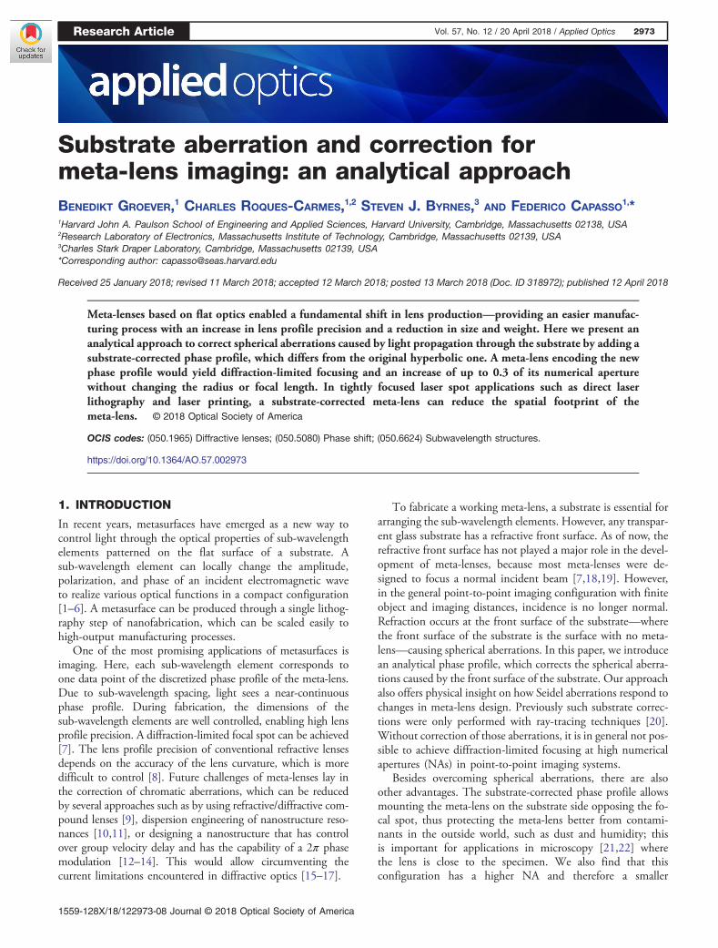
This formula gives the required shift at each radial coordi-nate to achieve diffraction-limited focusing at a focal length off . λ0 is the (free-space) illumination wavelength and nm is therefractive index of the ambient medium (nm � 1). Figure 1(a)shows the ray diagram of a meta-lens with a hyperbolic phaseprofile mounted on a substrate, referred to as a hyperbolicmeta-lens (HML) hereafter. Collimated light is incident fromthe front surface of the substrate. The meta-lens is mounted onthe other side of the substrate. The incident beam remains col-limated in the substrate. The HML performs diffracted-limitedfocusing. We refer to diffraction-limited focusing when all raysfor a given angle of incidence intersect the optical axis at thesame position. Amplitude variations of the incoming electricfield caused by absorption or reflection only need to be con-sidered once the system is diffraction-limited, as they influencethe shape of the focal spot, e.g., removal of the Airy disk causedby diffraction, which is known as apodization. Ray tracing issufficient to achieve diffraction-limited focusing. Figure 1(b)shows the performance of a HML when collimated light is in-cident from the meta-lens side. Here refraction in the substrateleads to a spherically aberrated focal spot. In this paper, wepresent an analytical approach to design a meta-lens to com-pensate for the refractive properties of the substrate, so thatwhen light is incident from the meta-lens side, it enables dif-fraction-limited focusing as shown in Fig. 1(d). The meta-lenswith a substrate-corrected phase profile, referred to as a sub-strate-corrected meta-lens (SCML) hereafter, has a larger phasegradient than a HML of the same focal length [Fig. 1(c)]. Thelarger phase gradient at the edge of the SCML corrects for lightpropagation through the substrate. Conversely, since theSCML is designed for light to be collimated on the meta-lensside, and if it is illuminated with collimated light from the sub-strate side, it results in a spherically aberrated focal spot asshown in Fig. 1(e). The fact that the HML and SCML arediffraction-limited only for one direction of incidence is not
specific to meta-lenses. Refractory plano-convex asphericallenses, which are used to focus collimated light, have the samekind of directional behavior. In what follows, we will refer to aconfiguration for a meta-lens as a “wrong” configuration whenit is illuminated in such a way as to produce a spherically aber-rated focal spot, and “right” configuration when illuminationresults in a diffraction-limited spot.
The minimum achievable focal spot size for a meta-lens usedin the wrong configuration is shown in Figs. 1(f ) and 1(g), re-spectively, for the HML and SCML. The figure of merit is theCircle of Confusion (CoC). The circle containing all incidentrays is an important figure of merit for the size of the focal spot.The CoC is defined as the minimum circle, when moving alongthe optical axis. Images are sharpest when the image detector isat this position. As each meta-lens is only diffraction-limited for
(a)
(c)
(d)
(e)
(f) (g)
(b)
Radial coordinate
FocusedFocusedFocused
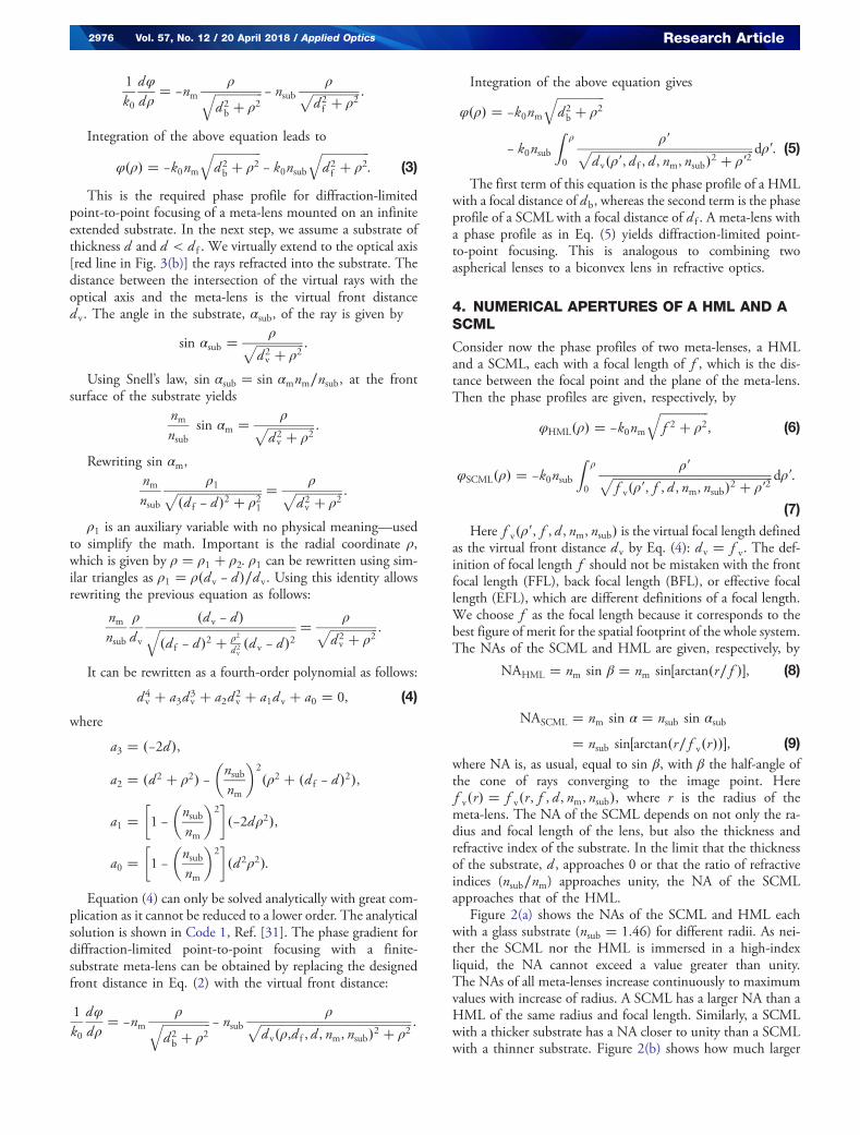
Fig. 1. Focusing of a HML and a SCML with incident collimatedlight from different sides of the substrate. (a) Ray diagram for diffrac-tion-limited focusing with the HML. Light is incident from the frontsurface of the substrate and every ray intersects the optical axis at thedesigned focal length. (b) Ray diagram for aberrated focusing with theHML. In this configuration, where light is incident from the backsideof the substrate, spherical aberration exists due to refraction at thefront surface of the substrate. (c) Phase profiles of the SCML andHML [Eqs. (6) and (7), respectively]. (d) Ray diagram for diffrac-tion-limited focusing with the SCML. Light is incident from themeta-lens side. The steeper phase profile of the SCML takes the re-fraction at the front surface of the substrate into account, in such a waythat every ray intersects with the optical axis at the same position.(e) Ray diagram for aberrated focusing with the SCML. Panels(f ) and (g) show CoC as a function of HML–SCML meta-lens radius,for light focused through different substrate thicknesses d . For allmeta-lenses depicted, f � 1.0 mm, nsub � 1.46, and nm � 1. Forthe meta-lenses in (a)–(e), substrate thickness d � 0.50 mm. Forthe meta-lenses in (c), illumination wavelength λ0 � 532 nm; the re-sults in the other subfigures are independent of the illumination wave-length as the 1∕k0 factor in the generalized Snell’s law cancels theillumination wavelength.
2974 Vol. 57, No. 12 / 20 April 2018 / Applied Optics Research Article
normal incidence in the right configuration, we consider onlynormal incidence in the wrong configuration. A rule of thumbto characterize a diffraction-limited system is to verify that allrays fall within a disk of diameter dAiry � 1.22�λ0∕NA�, whereNA is the NA. dAiry is roughly the diameter of the diffraction-limited Airy disk; when this criterion is satisfied, the point-spread function should be only modestly different from theideal Airy pattern. The diffraction-limited Airy disk as a func-tion of radius for the HML and SCML is shown as a shadedarea in Figs. 1(f ) and 1(g), respectively. Figure 1(f ) shows that aHML with a focal length of 1 mm used in the wrong configu-ration can still create a diffraction-limited spot if the NA issmaller than 0.3. Conversely, Fig. 1(g) shows that a SCMLwitha focal length of 1 mm used in the wrong configuration (i.e.,collimated on the substrate side) can be diffraction-limited upto a radius of 0.25 mm, corresponding to a NA of 0.3–0.4,depending on the thickness of the substrate [Fig. 2(b)].
The size of the Airy disk depends only on the NA of animaging system—not on the actual focal length or radius.When scaling the focal length and radius of the lens, theCoC scales with the same factor, but the size of the Airy diskdoes not change. Therefore, it is harder to achieve diffraction-limited focusing with a lens when the radius of the lensincreases.
3. PHASE PROFILE OF A DIFFRACTION-LIMITED POINT-TO-POINT FOCUSINGMETA-LENS
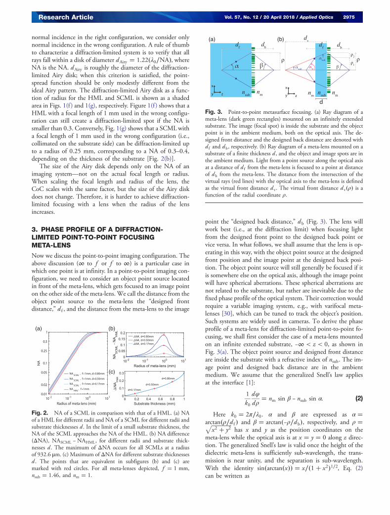
Now we discuss the point-to-point imaging configuration. Theabove discussion (∞ to f or f to ∞) is a particular case inwhich one point is at infinity. In a point-to-point imaging con-figuration, we need to consider an object point source locatedin front of the meta-lens, which gets focused to an image pointon the other side of the meta-lens. We call the distance from theobject point source to the meta-lens the “designed frontdistance,” d f , and the distance from the meta-lens to the image
point the “designed back distance,” d b (Fig. 3). The lens willwork best (i.e., at the diffraction limit) when focusing lightfrom the designed front point to the designed back point orvice versa. In what follows, we shall assume that the lens is op-erating in this way, with the object point source at the designedfront position and the image point at the designed back posi-tion. The object point source will still generally be focused if itis somewhere else on the optical axis, although the image pointwill have spherical aberrations. These spherical aberrations arenot related to the substrate, but rather are inevitable due to thefixed phase profile of the optical system. Their correction wouldrequire a variable imaging system, e.g., with varifocal meta-lenses [30], which can be tuned to track the object’s position.Such systems are widely used in cameras. To derive the phaseprofile of a meta-lens for diffraction-limited point-to-point fo-cusing, we shall first consider the case of a meta-lens mountedon an infinite extended substrate, −∞ < z < 0, as shown inFig. 3(a). The object point source and designed front distanceare inside the substrate with a refractive index of nsub. The im-age point and designed back distance are in the ambientmedium. We assume that the generalized Snell’s law appliesat the interface [1]:
1
k0
dφdρ
� nm sin β − nsub sin α: (2)
Here k0 � 2π∕λ0. α and β are expressed as α �arctan�ρ∕d f � and β � arctan�−ρ∕d b�, respectively, and ρ �ffiffiffiffiffiffiffiffiffiffiffiffiffiffiffi
x2 � y2p
has x and y as the position coordinates on themeta-lens while the optical axis is at x � y � 0 along z direc-tion. The generalized Snell’s law is valid once the height of thedielectric meta-lens is sufficiently sub-wavelength, the trans-mission is near unity, and the separation is sub-wavelength.With the identity sin�arctan�x�� � x∕�1� x2�1∕2, Eq. (2)can be written as
(a) (b)
(c)
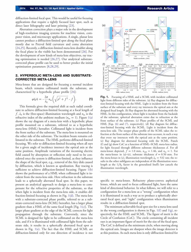
Fig. 2. NA of a SCML in comparison with that of a HML. (a) NAof a HML for different radii and NA of a SCML for different radii andsubstrate thicknesses d . In the limit of a small substrate thickness, theNA of the SCML approaches the NA of the HML. (b) NA difference(ΔNA), NASCML −NAHML, for different radii and substrate thick-nesses d . The maximum of ΔNA occurs for all SCMLs at a radiusof 932.6 μm. (c) Maximum of ΔNA for different substrate thicknessesd . The points that are equivalent in subfigures (b) and (c) aremarked with red circles. For all meta-lenses depicted, f � 1 mm,nsub � 1.46, and nm � 1.
(a) (b)
Fig. 3. Point-to-point metasurface focusing. (a) Ray diagram of ameta-lens (dark green rectangles) mounted on an infinitely extendedsubstrate. The image (focal spot) is inside the substrate and the objectpoint is in the ambient medium, both on the optical axis. The de-signed front distance and the designed back distance are denoted withd f and d b, respectively. (b) Ray diagram of a meta-lens mounted on asubstrate of a finite thickness d , and the object and image spots are inthe ambient medium. Light from a point source along the optical axisat a distance of d f from the meta-lens is focused to a point at distanceof d b from the meta-lens. The distance from the intersection of thevirtual rays (red lines) with the optical axis to the meta-lens is definedas the virtual front distance d v. The virtual front distance d v�ρ� is afunction of the radial coordinate ρ.
Research Article Vol. 57, No. 12 / 20 April 2018 / Applied Optics 2975
1
k0
dφdρ
� −nmρffiffiffiffiffiffiffiffiffiffiffiffiffiffiffiffi
d 2b � ρ2
q − nsubρffiffiffiffiffiffiffiffiffiffiffiffiffiffiffiffi
d 2f � ρ2
p :
Integration of the above equation leads to
φ�ρ� � −k0nmffiffiffiffiffiffiffiffiffiffiffiffiffiffiffiffid 2b � ρ2
q− k0nsub
ffiffiffiffiffiffiffiffiffiffiffiffiffiffiffiffid 2f � ρ2
q: (3)
This is the required phase profile for diffraction-limitedpoint-to-point focusing of a meta-lens mounted on an infiniteextended substrate. In the next step, we assume a substrate ofthickness d and d < d f . We virtually extend to the optical axis[red line in Fig. 3(b)] the rays refracted into the substrate. Thedistance between the intersection of the virtual rays with theoptical axis and the meta-lens is the virtual front distanced v. The angle in the substrate, αsub, of the ray is given by
sin αsub �ρffiffiffiffiffiffiffiffiffiffiffiffiffiffiffiffi
d 2v � ρ2
p :
Using Snell’s law, sin αsub � sin αmnm∕nsub, at the frontsurface of the substrate yields
nmnsub
sin αm � ρffiffiffiffiffiffiffiffiffiffiffiffiffiffiffiffid 2v � ρ2
p :
Rewriting sin αm,nmnsub
ρ1ffiffiffiffiffiffiffiffiffiffiffiffiffiffiffiffiffiffiffiffiffiffiffiffiffiffiffiffi�d f − d �2 � ρ21
p � ρffiffiffiffiffiffiffiffiffiffiffiffiffiffiffiffid 2v � ρ2
p :
ρ1 is an auxiliary variable with no physical meaning—usedto simplify the math. Important is the radial coordinate ρ,which is given by ρ � ρ1 � ρ2. ρ1 can be rewritten using sim-ilar triangles as ρ1 � ρ�d v − d �∕d v. Using this identity allowsrewriting the previous equation as follows:
nmnsub
ρ
d v
�d v − d �ffiffiffiffiffiffiffiffiffiffiffiffiffiffiffiffiffiffiffiffiffiffiffiffiffiffiffiffiffiffiffiffiffiffiffiffiffiffiffiffiffiffiffiffiffi�d f − d �2 � ρ2
d 2v�d v − d �2
q � ρffiffiffiffiffiffiffiffiffiffiffiffiffiffiffiffid 2v � ρ2
p :
It can be rewritten as a fourth-order polynomial as follows:
d 4v � a3d 3
v � a2d 2v � a1d v � a0 � 0, (4)
where
a3 � �−2d �,
a2 � �d 2 � ρ2� −�nsubnm
�2
�ρ2 � �d f − d �2�,
a1 ��1 −
�nsubnm
�2��−2dρ2�,
a0 ��1 −
�nsubnm
�2��d 2ρ2�:
Equation (4) can only be solved analytically with great com-plication as it cannot be reduced to a lower order. The analyticalsolution is shown in Code 1, Ref. [31]. The phase gradient fordiffraction-limited point-to-point focusing with a finite-substrate meta-lens can be obtained by replacing the designedfront distance in Eq. (2) with the virtual front distance:
1
k0
dφdρ
� −nmρffiffiffiffiffiffiffiffiffiffiffiffiffiffiffiffi
d 2b � ρ2
q − nsubρffiffiffiffiffiffiffiffiffiffiffiffiffiffiffiffiffiffiffiffiffiffiffiffiffiffiffiffiffiffiffiffiffiffiffiffiffiffiffiffiffiffiffiffiffiffiffiffiffiffi
d v�ρ,d f , d , nm, nsub�2 � ρ2p :
Integration of the above equation gives
φ�ρ� � −k0nmffiffiffiffiffiffiffiffiffiffiffiffiffiffiffiffid 2b � ρ2
q
− k0nsub
Zρ
0
ρ 0ffiffiffiffiffiffiffiffiffiffiffiffiffiffiffiffiffiffiffiffiffiffiffiffiffiffiffiffiffiffiffiffiffiffiffiffiffiffiffiffiffiffiffiffiffiffiffiffiffiffiffiffiffiffid v�ρ 0, d f , d , nm, nsub�2 � ρ 02p dρ 0: (5)
The first term of this equation is the phase profile of a HMLwith a focal distance of d b, whereas the second term is the phaseprofile of a SCML with a focal distance of d f . A meta-lens witha phase profile as in Eq. (5) yields diffraction-limited point-to-point focusing. This is analogous to combining twoaspherical lenses to a biconvex lens in refractive optics.
4. NUMERICAL APERTURES OF A HML AND ASCML
Consider now the phase profiles of two meta-lenses, a HMLand a SCML, each with a focal length of f , which is the dis-tance between the focal point and the plane of the meta-lens.Then the phase profiles are given, respectively, by
φHML�ρ� � −k0nmffiffiffiffiffiffiffiffiffiffiffiffiffiffiffiffif 2 � ρ2
q, (6)
φSCML�ρ� � −k0nsub
Zρ
0
ρ 0ffiffiffiffiffiffiffiffiffiffiffiffiffiffiffiffiffiffiffiffiffiffiffiffiffiffiffiffiffiffiffiffiffiffiffiffiffiffiffiffiffiffiffiffiffiffiffiffiffiffiffiffiffif v�ρ 0, f , d , nm, nsub�2 � ρ 02p dρ 0:
(7)
Here f v�ρ 0, f , d , nm, nsub� is the virtual focal length definedas the virtual front distance d v by Eq. (4): d v � f v. The def-inition of focal length f should not be mistaken with the frontfocal length (FFL), back focal length (BFL), or effective focallength (EFL), which are different definitions of a focal length.We choose f as the focal length because it corresponds to thebest figure of merit for the spatial footprint of the whole system.The NAs of the SCML and HML are given, respectively, by
NAHML � nm sin β � nm sin�arctan�r∕f ��, (8)
NASCML � nm sin α � nsub sin αsub
� nsub sin�arctan�r∕f v�r���, (9)where NA is, as usual, equal to sin β, with β the half-angle ofthe cone of rays converging to the image point. Heref v�r� � f v�r, f , d , nm, nsub�, where r is the radius of themeta-lens. The NA of the SCML depends on not only the ra-dius and focal length of the lens, but also the thickness andrefractive index of the substrate. In the limit that the thicknessof the substrate, d , approaches 0 or that the ratio of refractiveindices (nsub∕nm) approaches unity, the NA of the SCMLapproaches that of the HML.
Figure 2(a) shows the NAs of the SCML and HML eachwith a glass substrate (nsub � 1.46) for different radii. As nei-ther the SCML nor the HML is immersed in a high-indexliquid, the NA cannot exceed a value greater than unity.The NAs of all meta-lenses increase continuously to maximumvalues with increase of radius. A SCML has a larger NA than aHML of the same radius and focal length. Similarly, a SCMLwith a thicker substrate has a NA closer to unity than a SCMLwith a thinner substrate. Figure 2(b) shows how much larger
2976 Vol. 57, No. 12 / 20 April 2018 / Applied Optics Research Article
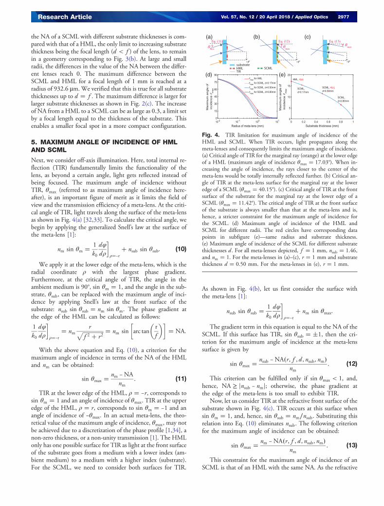
the NA of a SCML with different substrate thicknesses is com-pared with that of a HML, the only limit to increasing substratethickness being the focal length (d < f ) of the lens, to remainin a geometry corresponding to Fig. 3(b). At large and smallradii, the differences in the value of the NA between the differ-ent lenses reach 0. The maximum difference between theSCML and HML for a focal length of 1 mm is reached at aradius of 932.6 μm.We verified that this is true for all substratethicknesses up to d � f . The maximum difference is larger forlarger substrate thicknesses as shown in Fig. 2(c). The increaseof NA from a HML to a SCML can be as large as 0.3, a limit setby a focal length equal to the thickness of the substrate. Thisenables a smaller focal spot in a more compact configuration.
5. MAXIMUM ANGLE OF INCIDENCE OF HMLAND SCML
Next, we consider off-axis illumination. Here, total internal re-flection (TIR) fundamentally limits the functionality of thelens, as beyond a certain angle, light gets reflected instead ofbeing focused. The maximum angle of incidence withoutTIR, θmax (referred to as maximum angle of incidence here-after), is an important figure of merit as it limits the field ofview and the transmission efficiency of a meta-lens. At the criti-cal angle of TIR, light travels along the surface of the meta-lensas shown in Fig. 4(a) [32,33]. To calculate the critical angle, webegin by applying the generalized Snell’s law at the surface ofthe meta-lens [1]:
nm sin θm � 1
k0
dφdρ
�ρ�−r
� nsub sin θsub: (10)
We apply it at the lower edge of the meta-lens, which is theradial coordinate ρ with the largest phase gradient.Furthermore, at the critical angle of TIR, the angle in theambient medium is 90°, sin θm � 1, and the angle in the sub-strate, θsub, can be replaced with the maximum angle of inci-dence by applying Snell’s law at the front surface of thesubstrate: nsub sin θsub � nm sin θm. The phase gradient atthe edge of the HML can be calculated as follows:
1
k0
dφdρ
�ρ�−r
� nmrffiffiffiffiffiffiffiffiffiffiffiffiffiffiffiffi
f 2 � r2p � nm sin
�arc tan
�r
f
��� NA:
With the above equation and Eq. (10), a criterion for themaximum angle of incidence in terms of the NA of the HMLand nm can be obtained:
sin θmax �nm −NA
nm: (11)
TIR at the lower edge of the HML, ρ � −r, corresponds tosin θm � 1 and an angle of incidence of θmax. TIR at the upperedge of the HML, ρ � r, corresponds to sin θm � −1 and anangle of incidence of −θmax. In an actual meta-lens, the theo-retical value of the maximum angle of incidence, θmax, may notbe achieved due to a discretization of the phase profile [1,34], anon-zero thickness, or a non-unity transmission [1]. The HMLonly has one possible surface for TIR as light at the front surfaceof the substrate goes from a medium with a lower index (am-bient medium) to a medium with a higher index (substrate).For the SCML, we need to consider both surfaces for TIR.
As shown in Fig. 4(b), let us first consider the surface withthe meta-lens [1]:
nsub sin θsub �1
k0
dφdρ
�ρ�−r
� nm sin θmax:
The gradient term in this equation is equal to the NA of theSCML. If this surface has TIR, sin θsub � �1, then the cri-terion for the maximum angle of incidence at the meta-lenssurface is given by
sin θmax �nsub −NA�r, f , d , nsub, nm�
nm: (12)
This criterion can be fulfilled only if sin θmax < 1, and,hence, NA ≥ jnsub − nmj; otherwise, the phase gradient atthe edge of the meta-lens is too small to exhibit TIR.
Now, let us consider TIR at the refractive front surface of thesubstrate shown in Fig. 4(c). TIR occurs at this surface whensin θm � 1, and, hence, sin θsub � nm∕nsub. Substituting thisrelation into Eq. (10) eliminates nsub. The following criterionfor the maximum angle of incidence can be obtained:
sin θmax �nm −NA�r, f , d , nsub, nm�
nm: (13)
This constraint for the maximum angle of incidence of anSCML is that of an HML with the same NA. As the refractive
(a) (b) (c)
(d) (e)
Fig. 4. TIR limitation for maximum angle of incidence of theHML and SCML. When TIR occurs, light propagates along themeta-lenses and consequently limits the maximum angle of incidence.(a) Critical angle of TIR for the marginal ray (orange) at the lower edgeof a HML (maximum angle of incidence θmax � 17.03°). When in-creasing the angle of incidence, the rays closer to the center of themeta-lens would be totally internally reflected further. (b) Critical an-gle of TIR at the meta-lens surface for the marginal ray at the loweredge of a SCML (θmax � 40.15°). (c) Critical angle of TIR at the frontsurface of the substrate for the marginal ray at the lower edge of aSCML (θmax � 11.42°). The critical angle of TIR at the front surfaceof the substrate is always smaller than that at the meta-lens and is,hence, a stricter constraint for the maximum angle of incidence forthe SCML. (d) Maximum angle of incidence of the HML andSCML for different radii. The red circles have corresponding datapoints in subfigure (e)—same radius and substrate thickness.(e) Maximum angle of incidence of the SCML for different substratethicknesses d . For all meta-lenses depicted, f � 1 mm, nsub � 1.46,and nm � 1. For the meta-lenses in (a)–(c), r � 1 mm and substratethickness d � 0.50 mm. For the meta-lenses in (e), r � 1 mm.
Research Article Vol. 57, No. 12 / 20 April 2018 / Applied Optics 2977
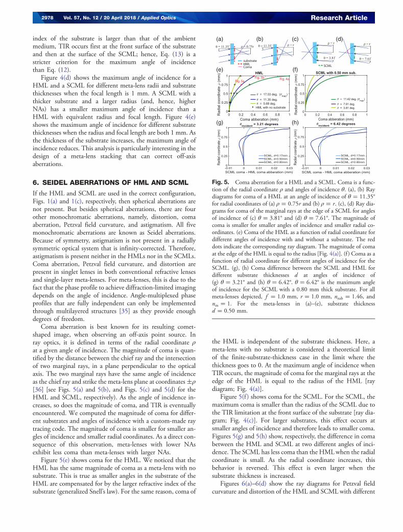
index of the substrate is larger than that of the ambientmedium, TIR occurs first at the front surface of the substrateand then at the surface of the SCML; hence, Eq. (13) is astricter criterion for the maximum angle of incidencethan Eq. (12).
Figure 4(d) shows the maximum angle of incidence for aHML and a SCML for different meta-lens radii and substratethicknesses when the focal length is 1 mm. A SCML with athicker substrate and a larger radius (and, hence, higherNAs) has a smaller maximum angle of incidence than aHML with equivalent radius and focal length. Figure 4(e)shows the maximum angle of incidence for different substratethicknesses when the radius and focal length are both 1 mm. Asthe thickness of the substrate increases, the maximum angle ofincidence reduces. This analysis is particularly interesting in thedesign of a meta-lens stacking that can correct off-axisaberrations.
6. SEIDEL ABERRATIONS OF HML AND SCML
If the HML and SCML are used in the correct configuration,Figs. 1(a) and 1(c), respectively, then spherical aberrations arenot present. But besides spherical aberrations, there are fourother monochromatic aberrations, namely, distortion, comaaberration, Petzval field curvature, and astigmatism. All fivemonochromatic aberrations are known as Seidel aberrations.Because of symmetry, astigmatism is not present in a radiallysymmetric optical system that is infinity-corrected. Therefore,astigmatism is present neither in the HMLs nor in the SCMLs.Coma aberration, Petzval field curvature, and distortion arepresent in singlet lenses in both conventional refractive lensesand single-layer meta-lenses. For meta-lenses, this is due to thefact that the phase profile to achieve diffraction-limited imagingdepends on the angle of incidence. Angle-multiplexed phaseprofiles that are fully independent can only be implementedthrough multilayered structures [35] as they provide enoughdegrees of freedom.
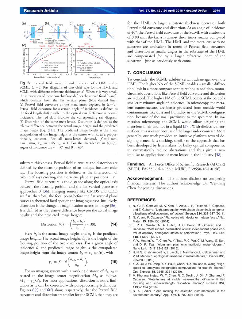
Coma aberration is best known for its resulting comet-shaped image, when observing an off-axis point source. Inray optics, it is defined in terms of the radial coordinate ρat a given angle of incidence. The magnitude of coma is quan-tified by the distance between the chief ray and the intersectionof two marginal rays, in a plane perpendicular to the opticalaxis. The two marginal rays have the same angle of incidenceas the chief ray and strike the meta-lens plane at coordinates�ρ[36] [see Figs. 5(a) and 5(b), and Figs. 5(c) and 5(d) for theHML and SCML, respectively). As the angle of incidence in-creases, so does the magnitude of coma, and TIR is eventuallyencountered. We computed the magnitude of coma for differ-ent substrates and angles of incidence with a custom-made raytracing code. The magnitude of coma is smaller for smaller an-gles of incidence and smaller radial coordinates. As a direct con-sequence of this observation, meta-lenses with lower NAsexhibit less coma than meta-lenses with larger NAs.
Figure 5(e) shows coma for the HML. We noticed that theHML has the same magnitude of coma as a meta-lens with nosubstrate. This is true as smaller angles in the substrate of theHML are compensated for by the larger refractive index of thesubstrate (generalized Snell’s law). For the same reason, coma of
the HML is independent of the substrate thickness. Here, ameta-lens with no substrate is considered a theoretical limitof the finite-substrate-thickness case in the limit where thethickness goes to 0. At the maximum angle of incidence whenTIR occurs, the magnitude of coma for the marginal rays at theedge of the HML is equal to the radius of the HML [raydiagram; Fig. 4(a)].
Figure 5(f ) shows coma for the SCML. For the SCML, themaximum coma is smaller than the radius of the SCML due tothe TIR limitation at the front surface of the substrate [ray dia-gram; Fig. 4(c)]. For larger substrates, this effect occurs atsmaller angles of incidence and therefore leads to smaller coma.Figures 5(g) and 5(h) show, respectively, the difference in comabetween the HML and SCML at two different angles of inci-dence. The SCML has less coma than the HMLwhen the radialcoordinate is small. As the radial coordinate increases, thisbehavior is reversed. This effect is even larger when thesubstrate thickness is increased.
Figures 6(a)–6(d) show the ray diagrams for Petzval fieldcurvature and distortion of the HML and SCML with different
(a) (b) (c) (d)
(e) (f)
(g) (h)
Fig. 5. Coma aberration for a HML and a SCML. Coma is a func-tion of the radial coordinate ρ and angles of incidence θ. (a), (b) Raydiagrams for coma of a HML at an angle of incidence of θ � 11.35°for radial coordinates of (a) ρ � 0.75r and (b) ρ � r. (c), (d) Ray dia-grams for coma of the marginal rays at the edge of a SCML for anglesof incidence of (c) θ � 3.81° and (d) θ � 7.61°. The magnitude ofcoma is smaller for smaller angles of incidence and smaller radial co-ordinates. (e) Coma of the HML as a function of radial coordinate fordifferent angles of incidence with and without a substrate. The reddots indicate the corresponding ray diagram. The magnitude of comaat the edge of the HML is equal to the radius [Fig. 4(a)]. (f ) Coma as afunction of radial coordinate for different angles of incidence for theSCML. (g), (h) Coma difference between the SCML and HML fordifferent substrate thicknesses d at angles of incidence of(g) θ � 3.21° and (h) θ � 6.42°. θ � 6.42° is the maximum angleof incidence for the SCML with a 0.80 mm thick substrate. For allmeta-lenses depicted, f � 1.0 mm, r � 1.0 mm, nsub � 1.46, andnm � 1. For the meta-lenses in (a)–(e), substrate thicknessd � 0.50 mm.
2978 Vol. 57, No. 12 / 20 April 2018 / Applied Optics Research Article
substrate thicknesses. Petzval field curvature and distortion aredefined by the focusing position of an oblique incident chiefray. The focusing position is defined as the intersection oftwo chief rays crossing the meta-lens plane at positions �ϵ.
Petzval field curvature is the distance along the optical axisbetween the focusing position and the flat vertical plane as ϵapproaches 0 [36]. Imaging sensors like CMOS and CDDare flat; therefore, the focal point before the flat vertical planecauses an aberrated focal spot on the imaging sensor. Intuitively,distortion is the change in magnification across an image [36].It is defined as the relative difference between the actual imageheight and the predicted image height:
Distortion�%� ��ha − hpha
�· 100: (14)
Here ha is the actual image height and hp is the predictedimage height. The actual image height, ha, is the height of thefocusing position of the two chief rays. For a given angle ofincidence θ, the predicted image height is the extrapolatedimage height from the image center: hp � γ0 tan�θ�, with
γ0 � f − d�nsub − nm
nm
�: (15)
For an imaging system with a working distance of d f , γ0 isrelated to the image center magnification M 0 as follows:M 0 � γ0∕d f . For most applications, distortion is not a limi-tation as it can be corrected with post-processing techniques.Figures 6(e) and 6(f ) show, respectively, that the Petzval fieldcurvature and distortion are smaller for the SCML than they are
for the HML. A larger substrate thickness decreases bothPetzval field curvature and distortion. At an angle of incidenceof 40°, the Petzval field curvature of the SCML with a substrateof 0.80 mm thickness is almost three times smaller comparedwith that of the HML. The HML and the meta-lens with nosubstrate are equivalent in terms of Petzval field curvatureand distortion as smaller angles in the substrate of the HMLare compensated for by a larger refractive index of thesubstrate—just as previously with coma.
7. CONCLUSION
To conclude, the SCML exhibits certain advantages over theHML. The higher NA of the SCML enables a smaller diffrac-tion limit in a more compact configuration; in addition, mono-chromatic aberrations like Petzval field curvature and distortionare reduced. The higher NA of the SCML comes at the cost of asmaller maximum angle of incidence. In microscopy, the meta-lens nanostructures are better protected from outside worldcontaminants like dust and humidity in the SCML configura-tion, because of the small proximity to the specimen. In im-mersion microscopy, the SCML would allow designing themeta-lens in air and not in a liquid [37]. With dielectric meta-surfaces, this is easier because of the larger index contrast. Moregenerally, our work provides an intuitive platform toward de-signing a meta-lens stacking, similar to the approach that hasbeen developed by lens makers for bulky optical components,to systematically reduce aberrations and thus give a newimpulse to applications of meta-lenses in the industry [38].
Funding. Air Force Office of Scientific Research (AFOSR)(MURI, FA9550-14-1-0389, MURI, FA9550-16-1-0156).
Acknowledgment. The authors disclose no competingfinancial interests. The authors acknowledge Dr. Wei-TingChen for joining discussions.
REFERENCES1. N. Yu, P. Genevet, M. A. Kats, F. Aieta, J. P. Tetienne, F. Capasso,
and Z. Gaburro, “Light propagation with phase discontinuities: gener-alized laws of reflection and refraction,” Science 334, 333–337 (2011).
2. N. Yu and F. Capasso, “Flat optics with designer metasurfaces,” Nat.Mater. 13, 139–150 (2014).
3. J. P. B. Mueller, N. A. Rubin, R. C. Devlin, B. Groever, and F.Capasso, “Metasurface polarization optics: independent phase con-trol of arbitrary orthogonal states of polarization,” Phys. Rev. Lett.118, 113901 (2017).
4. Y. W. Huang, W. T. Chen, W. Y. Tsai, P. C. Wu, C. M. Wang, G. Sun,and D. P. Tsai, “Aluminum plasmonic multicolor meta-hologram,”Nano Lett. 15, 3122–3127 (2015).
5. H. N. S. Krishnamoorthy, Z. Jacob, E. Narimanov, I. Kretzschmar, andV. M. Menon, “Topological transitions in metamaterials,” Science 336,205–209 (2012).
6. Y. Z. Liu, J. W. Dong, Y. Y. Pu, B. Chen, H. X. He, and H. Wang, “High-speed full analytical holographic computations for true-life scenes,”Opt. Express 18, 3345–3351 (2010).
7. M. Khorasaninejad, W. T. Chen, R. C. Devlin, J. Oh, A. Zhu, and F.Capasso, “Meta-lenses at visible wavelengths: diffraction-limitedfocusing and sub-wavelength resolution imaging,” Science 352,1190–1194 (2016).
8. S. A. Bedini, “Lens making for scientific instrumentation in theseventeenth century,” Appl. Opt. 5, 687–694 (1996).
(a) (b) (c) (d)
(e) (f)
Fig. 6. Petzval field curvature and distortion of a HML and aSCML. (a)–(d) Ray diagrams of two chief rays for the HML andSCML with different substrate thicknesses d . When ϵ is very small,the intersection of those two chief rays defines the curved focal “plane”,which deviates from the flat vertical plane (blue dashed line).(e) Petzval field curvature of the meta-lenses depicted in (a)–(d).Petzval field curvature for a certain angle of incidence is defined asthe focal length shift parallel to the optical axis. Reference is normalincidence. The red dots indicate the corresponding ray diagram.(f ) Distortion of the same meta-lenses. Distortion is defined as therelative difference between the actual image height and the predictedimage height [Eq. (14)]. The predicted image height is the linearextrapolation of the image height at the center with γ0 as a propor-tionality constant. For all meta-lenses depicted, f � 1 mm,r � 1 mm, nsub � 1.46, nm � 1. For the meta-lenses in (a)–(d),angles of incidence are θ � 0° and θ � 40°.
Research Article Vol. 57, No. 12 / 20 April 2018 / Applied Optics 2979
9. T. Stone and N. George, “Hybrid diffractive-refractive lenses andachromats,” Appl. Opt. 27, 2960–2971 (1988).
10. D. Faklis and G. M. Morris, “Spectral properties of multiorderdiffractive lenses,” Appl. Opt. 34, 2462–2468 (1995).
11. D. W. Sweeney and G. E. Sommargren, “Harmonic diffractive lenses,”Appl. Opt. 34, 2469–2475 (1995).
12. F. Aieta, M. A. Kats, P. Genevet, and F. Capasso, “Multiwavelengthachromatic metasurfaces by dispersive phase compensation,”Science 347, 1342–1345 (2015).
13. M. Khorasaninejad, Z. Shi, A. Zhu, W. T. Chen, V. Sanjeev, and F.Capasso, “Achromatic meta-lens over 60 nm bandwidth in the visibleand metalens with reverse chromatic dispersion,” Nano Lett. 17,1819–1824 (2017).
14. S.Wang, P. C.Wu, V. Su, Y.-C. Lai, C. Hung Chu, J.-W. Chen, S.-H. Lu,J. Chen, B. Xu, C.-H. Kuan, T. Li, S. Zhu, and D. P. Tsai, “Broadbandachromatic optical metasurface devices,” Nat. Commun. 8, 187 (2017).
15. Y. Soskind, Field Guide to Diffractive Optics (SPIE, 2011).16. G. J. Swanson, “Binary optics technology: the theory and design of
multi-level diffractive optical elements,” Technical Report 854, DTICDocument (Lincoln Laboratory, 1989).
17. M. B. Stern, “Binary optics: a VLSI-based microoptics technology,”Microelectron. Eng. 32, 369–388 (1996).
18. M. Khorasaninejad, F. Aieta, P. Kanhaiya, M. A. Kats, P. Genevet, D.Rousso, and F. Capasso, “Achromatic metasurface lens at telecom-munication wavelengths,” Nano Lett. 15, 5358–5362 (2015).
19. M. Khorasaninejad, W. T. Chen, J. Oh, and F. Capasso, “Super-dispersive off-axis meta-lenses for compact high resolution spectros-copy,” Nano Lett. 16, 3732–3737 (2016).
20. A.Arbabi,Y.Horie,A.J.Ball,M.Bagheri,andA.Faraon, “Subwavelength-thick lenses with high numerical apertures and large efficiency based onhigh-contrast transmitarrays,” arXiv:1410.8261 (2014).
21. K. Esswein, “Attachment of microscope objectives,” U.S. patent4,515,439 (07 May 1985).
22. M. Abramowitz, K. R. Spring, H. E. Keller, and M. W. Davidson, “Basicprinciples of microscope objectives,” BioTechniques 33, 772–781(2002).
23. T. Ito and S. Okazaki, “Pushing the limits of lithography,” Nature 406,1027–1031 (2000).
24. F. Aieta, P. Genevet, M. A. Kats, N. Yu, R. Blanchard, Z. Gaburro, andF. Capasso, “Aberration-free ultrathin flat lenses and axicons at
telecom wavelengths based on plasmonic metasurfaces,” NanoLett. 12, 4932–4936 (2012).
25. F. Aieta, P. Genevet, M. Kats, and F. Capasso, “Aberrations offlat lenses and aplanatic metasurfaces,” Opt. Express 21,31530–31539 (2013).
26. B. Groever, W. T. Chen, and F. Capasso, “Meta-lens doublet in thevisible,” Nano Lett. 17, 4902–4907 (2017).
27. A. Arbabi, E. Arbabi, S. M. Kamali, Y. Horie, S. Han, and A. Faraon,“Miniature optical planar camera based on a wide-angle metasurfacedoublet corrected for monochromatic aberrations,” Nat. Commun. 7,13682 (2016).
28. F. Bociort, “Optical system optimization,” in Encyclopedia of OpticalEngineering (2003), Vol. 2, pp. 1843–1850.
29. M. Peschka, F. Blechinger, H. Gross, and H. Zuegge, Handbook ofOptical Systems: Vol. 3. Aberration Theory and Correction of OpticalSystems (Wiley, 2007).
30. A. She, S. Zhang, S. Shian, D. R. Clarke, and F. Capasso, “Large areaelectrically tunable lenses based on metasurfaces and dielectricelastomer actuators,” arXiv:1708.01972 (2017).
31. B. Groever, “Matlab code for virtual focal length,” (2017) [Retrieved 23October 2017]; https://doi.org/10.6084/m9.figshare.5527954.
32. S. Sun, Q. He, S. Xiao, Q. Xu, X. Li, and L. Zhou, “Gradient-indexmeta-surfaces as a bridge linking propagating waves and surfacewaves,” Nat. Mater. 11, 426–431 (2012).
33. S. Sun, K.-Y. Yang, C.-M. Wang, T.-K. Juan, W. T. Chen, C. Y. Liao,Q. He, S. Xiao, W.-T. Kung, G.-Y. Guo, L. Zhou, and D. P. Tsai, “High-efficiency broadband anomalous reflection by gradient meta-surfaces,” Nano Lett. 12, 6223–6229 (2012).
34. B. C. Kress and P. Meyrueis, Applied Digital Optics: From Micro-optics to Nanophotonics (Wiley, 2009).
35. Z. Lin, B. Groever, F. Capasso, A. W. Rodriguez, and M. Loncar,“Topology optimized multi-layered meta-optics,” arXiv:1706.06715(2017).
36. W. J. Smith, Modern Optical Engineering (Tata McGraw-HillEducation, 1966).
37. W. T. Chen, A. Y. Zhu, M. Khorasaninejad, Z. Shi, V. Sanjeev, and F.Capasso, “Immersion meta-lenses at visible wavelengths for nano-scale imaging,” Nano Lett. 17, 3188–3194 (2017).
38. R. Kingslake, A History of the Photographic Lens (Elsevier,1989).
2980 Vol. 57, No. 12 / 20 April 2018 / Applied Optics Research Article