Embed Size (px)
Citation preview

Subwavelength Design: Lithography Effects and Challenges
Part II: EDA Implications
Andrew B. Kahng, UCLA Computer Science Dept.
ISQED-2000 Tutorial
March 20, 2000

Forcing Trends in EDA
• Silicon complexity and design complexity– many opportunities to leave major $$$ on the table– issues: physical effects of process, migratability– design rules more conservative, design waivers – device-level layout opts in cell-based methodologies
• Verification cost increases dramatically• Prevention a necessary complement to checking • Successive approximation = design convergence
– upstream activities pass intentions, assumptions downstream – downstream activities must be predictable– models of analysis/verification == objectives for synthesis

EDA Awareness of Process
EDA wants to know as little as possible
This part of tutorial: the unavoidable issues

Necessary Formulations, Flows
• Upstream objectives want to capture downstream layout operations “transparently”
• New problem formulations– PSM: more global phenomena, scalability issues– OPC: mostly local phenomena– function-driven corrections– hierarchical and reuse-centric regimes
• New tool integrations

Phase Smart Custom LayoutPhase Smart Custom Layout
PhaseConflict
Detection
AnyConflicts?
Yes
LayoutEditing
PhaseConflict
Resolution
No
Phase CompliantCells and Cores
PhaseConflictInterface

Phase Smart Place and Route
Phase Smart Placement Phase Smart Routing
No
PhaseConflict
Detection
AnyConflicts?
Yes
Placement
PhaseConflict
Resolution
PhaseConflict
Detection
AnyConflicts?
Yes
Routing
PhaseConflict
Resolution
No
Phase CompliantCells and Cores
Phase CompliantLayout

SubW avelength EnhancedPhysical Verification
OPC
SiliconDRC
SiliconImage
Generator
W ithinTolerance ? Yes
No
PhaseCompliant
LayoutDatabase
Phase ShiftLayout Design
Phase ShiftLayout
VerificationInterface
VAMPIRE
Extraction
LVS
DRC
Phase Smart Verification

Global phenomena in PSM phase layout

Phase Assignment in PSM
Features Conflict areas (<B)
0 0180
< B > B
Assign 0, 180 phase regions such that:• (dark field) feature pairs with separation < B have opposite phases
• (bright field) features with width < B are induced by adjacent phase regions with opposite phases
b minimum separation or width, with phase shifting
B minimum separation or width, without phase shifting
b(Dark field, neg resist)

Conflict Graph
< B
Vertices: features (or phase regions)
Edges: “conflicts” (necessary phase contrasts)
(feature pairs with separation < B )

Odd Cycles in Conflict Graph
• Self-consistent phase assignment is not possible if there is an odd cycle in the conflict graph
• Phase-assignable bipartite no odd cycles
0 phase 180 phase
??? phase

Breaking Odd Cycles
B
• Must change the layout:• change feature dimensions, and/or • change spacings• PSM phase-assignability is a layout, not verification, issue

blue features
green 180-shift
black boundariesb/w 0 and 180 areas(to be deleted)
red odd degree
Bright-Field (Positive-Resist) Context• Every critical-width feature defined by opposite-phase regions
• Regions not defined a priori
Value Proposition to Designers
• 0.10m feature sizes in production in 1999 2x performance
– Higher yield
– “Transparent” to designer
Benefit Gate-PSM Full PSMSpeed ++++ ++++Yield ++++ ++++Power ++ ++++Die Size N/A ++++Initial Generation 0.35 m - 0.25 m 0.15 m

Problem Statements I• Develop efficient algorithms for minimum-cost
phase region definition and phase assignment in bright-field context– open: definition of cost (mfg difficulty, area, …)
• Continuum between sparse, dense criticality– DF Alt PSM + BF binary trim mask approach simple and
elegant for sparse critical features– what about when all features are critical? (full-chip area opt, in addition to gate shrink)– can be treated as a routing problem (of phase edges)

Problem Statements II
• New logic (mapping) and performance optimization formulations– with phase shifting, gate lengths and wire widths
continuously variable between b and B– without phase shifting, gate lengths and wire widths
must be at least B– not all features can be phase-shifted: function-driven
What is optimal choice of phase-shifted features, and their sizes?

Problem Statements III
• Understand PSM implications for custom layout– define a taxonomy of phase conflict– no set of traditional design rules can handle all phase
conflicts what are “good layout practices”?• “no T’s on poly”
• “fingered transistors should have even-length fingers”
• etc.
• Address PSM as a multi-layer problem– e.g., conflict can be solved by re-routing a connection to
another layer

Layer Assignment

Local phenomena in OPC

Problem Statements IV
• Pass functional intent down to OPC insertion– OPC insertion is for predictable circuit performance,
function– Problem: make only corrections that win $$$,
reduce perf variation (i.e., link to performance analysis, optimization) ?
• Pass limits of mask verification up to layout– Problem: avoid making corrections that can’t be
manufactured or verified

Problem Statements V
• Minimize data volume– Problem: make corrections that win $$$, reduce perf
variation up to some limit of data volume for resulting layout (== mask complexity, cost)
• Layout needs models of OPC insertion process– Problem: taxonomize implications of layout geometry
on cost of the OPC that is required to yield function or “faithfully” print the geometry
– find a realistic cost model for breaking hierarchy (including verification, characterization costs)

Hierarchical and Reuse-Centric Contexts

Problem Statements VI
• Given a cell library, what is its flexibility (i.e., composability with respect to PSM) ?
• Given a standard-cell layout and allowed increase in hierarchical layout data volume, what is the maximum reduction in area obtainable by creating new cell masters with different phase layout solutions?
• Given a standard-cell layout with phase-solution instantiations that induce conflicts, what is minimum-cost removal of phase conflicts?– DOF’s: change instance, shift, space, mirror, ...

Integrated Layout Flow, 1• Gate-level netlist, performance constraint budgeting,
early context (mask/litho technology, area density...)• Standard-cell placement with integrated compatibility
awareness (composable PSM layouts)• Global and detailed routing, cell resynthesis on fly
– delay, noise, reliability assumptions = constraints– OPC- and PSM-aware min-cost layout synthesis subject to
constraints (e.g., minimize costs of breaking hierarchy, follow “good practices”, etc.)
– fill abstractions (for parasitic extraction) in constraint-driven routing

Integrated Layout Flow, 2
• Density analysis, CMP-fill estimation based on detailed routing
• Post-detailed routing performance analysis• PSM phase assignability check for all layers
– new compaction constraints as necessary
– layout compaction or incremental detailed routing
– until pass phase assignability, performance analysis
– note: integration with full-chip geometric compaction!
• Actual dummy fill insertion– issues: data volume

Integrated Layout Flow, 3
• Detailed physical verification (geom, conn, perf)• Full-chip OPC insertion
– issues: min-cost OPC that achieves required function
– issues: data volumes, metrics, intermediate formats
– issues: tools stepping on each other (line extensions in DSM router rules are “zeroth-order OPC”, for example)
• Full-chip printability check• Silicon-level DRC/LVS/performance analysis

Conclusions
• New problem formulations– PSM: layout practices, automated full-chip and standard-cell
compatible solutions– OPC: taxonomy of local phenomena, data reduction– function-driven corrections (can filter complexity)– hierarchy, data volume, reuse concerns
• New tool integrations– compaction, on-the-fly cell synthesis, incremental detailed
routing– graph-based (verification-type) layout analyses– new performance opts, even logic opts

Example Details I:
Automatic Conflict Resolution

Compaction-Oriented Approach
• Analyze input layout• Determine constraints for output layout
– new PSM-induced (shape, spacing) constraints• Compact (e.g., solve LP) with min
perturbation objective– e.g., minimize sum of differences between old
and new positions of each edge • Key: Minimize the set of new constraints,
i.e., break all odd cycles in conflict graph by deleting a minimum number of edges.

One-Shot Phase Assignment
conflict graph
compaction
phase assignment
find min-cost edge set to be deleted for 2-colorability

Conflict Graph• Dark Field: build graph over feature regions
• edge between two features whose separation is < B
• Bright Field: build graph over shifter regions • two edge types • adjacency edge between overlapping phase regions : endpoints must have same phase
– essentially, these regions must be “merged” into single phase shifter– DRC-like (gap, notch type) local rules must likely be applied to such “merging”
• conflict edge between shifters on opposite side of critical feature: endpoints must have opposite phase • Step 3: simple reduction to previous (dark-field) T-join solution: each dotted edge becomes a 2-chain
(introduce one extra vertex)

Conflict Graph
• Dark Field:
conflict graph Ggreen = feature; red = conflict
• Bright Field: conflict edge
adjacency edge
conflict graph G

Conflict Graph for Cell-Based Layouts• Coarse view: at level of connected components of
conflict graphs within each cell master• each of these components is independently phase-assignable• can be treated as a single “vertex” in coarse-grain conflict graph
edge in coarse-grain conflict graph
cell master A cell master Bconnected component

Detail: Conflict Edge Weight
• Conflict edges not on critical path: break for free• Or, use min-perturbation objective
critical path

F4
F2
F3
F1
S1
S2
S3
S5
S4
S6
S7 S8

Black points - shiftersBlue - shifter overlapThick edges - critical
Bipartization Problem: delete min # of thin edges to make graph bipartite

Black points - featuresBlue - shifter overlapPink - extra nodes to distinguish opposite shifters
Bipartization Problem: delete min # of nodes (or edges) to make graph bipartite

Black points - shiftersBlue - shifter overlapThick edges - criticalBipartization Problem: delete min # of thin edges
to make graph bipartite

Black points - featuresBlue - shifter overlapPink - extra nodes to distinguish opposite shifters
Bipartization Problem: delete min # of nodes (or edges) to make graph bipartite

Key Technique: Reduction to T-join
• Goal: delete minimum-cost set of edges from conflict graph G, so as to eliminate odd cycles
• Construct geometric dual graph D = dual(G)• Find odd-degree vertices T in D• Solve the T-join problem in D:
– find min-weight edge set J in D such that• all T-vertices have odd degree w.r.t. J• all other vertices have even degree w.r.t. J
• Solution J corresponds to the desired min-cost edge set in conflict graph G

Optimal Odd Cycle Elimination
conflict graph G
dual graph DT-join of odd-degree nodes in D
dark green = feature; red = conflict

Optimal Odd Cycle Elimination
corresponds to broken edges in original conflict graph
- assign phases: dark green and purple- remaining red conflicts correctly handled
T-join of odd-degree nodes in D
dark green = feature; red = conflict
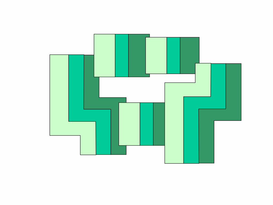
T-join Problem in Sparse Graphs• Reduction to matching
– construct a complete graph T(G)• vertices = T-vertices• edge costs = shortest-path cost
– find minimum-cost perfect matching• Typical example = sparse (not always planar) graph
– note that conflict graphs are sparse– #vertices = 1,000,000 – #edges 5 #vertices– # T-vertices 10% of #vertices = 100,000
• Drawback: finding all shortest paths too slow and memory-consuming – #vertices = 100,000 #edges = 5,000,000,000

T-join Problem: Reduction to Matching
• Desirable properties of reduction to matching:– exact (i.e., optimal)– not much memory (say 2-3Xmore) – results in a very fast solution
• Solution: gadgets!– replace each edge/vertex with gadgets s.t.
matching all vertices in gadgeted graph
T-join in original graph

T-join Problem: Reduction to Matching• replace each vertex with a chain of triangles• one more edge for T-vertices• in graph D: m = #edges, n = #vertices, t = #T• in gadgeted graph: 4m-2n-t vertices, 7m-5n-t edges• cost of red edges = original dual edge costs
cost of (black) edges in triangles = 0
vertex in T
vertex T

Example of Gadgeted Graph
Dual Graph
Gadgeted graph
black + red edges ==min-cost perfect matching

Results
Layout1 Layout2 Layout3Testcase polygons edges polygons edges polygons edges
3769 12442 9775 26520 18249 51402
Algorithm edges runtime edges runtime edges runtimeGreedy 2650 0.56 2722 3.66 6180 5.38
GW 1612 3.33 1488 5.77 3280 14.47Exact 1468 19.88 1346 16.67 2958 74.33
• Runtimes in CPU seconds on Sun Ultra-10• Greedy = breadth-first-search bicoloring (similar to Ooi et al.)• GW = Goemans/Williamson95 heuristic• Cook/Rohe98 for perfect matchingLatest improved gadgets: runtimes decrease by factor of 6

Example Details II:
Auto-P&R Flow Issues

Constraints• PSM must be “transparent” to ASIC auto-P&R
– “free composability” is the cornerstone of the cell-based methodology!– focus on poly layer we are concerned with placer, not router
• Competitive context for placer– extremely competitive runtime regimes (e.g., 106 cells detail-placed in 20 min);
faster runtimes needed in RTL-planning methodologies (Nano/PKS, Tera)– any nontrivial cost of checking placement phase-assignability is unacceptable
• Iteration between placer and a separate tool is unacceptable
– interface to auto-P&R tools is bulky (e.g., 100s of MB for DEF), slow– no known convergent method for post-P&R phase-assignability checks to drive
P&R to guaranteed correct solution (very difficult!)
• P&R tool MUST deliver guaranteed phase-assignable poly layer

Guidelines• Placer
– no re-entry into placer from an external tool• any needed extra functionality must be built directly into placer
– placer must guarantee a phase-assignable poly when finished– polygon layout information currently not in placement vocabulary
• available relevant abstractions: pin EEQs/LEQs, overlap layer geometries
• side files or LEF extensions needed for, e.g., capturing versioning or phase shifters near left/right cell boundaries
• Cell layout– cell layouts and phase shifters are assumed fixed during library
creation• on-the-fly cell layout synthesis or layout perturbations generally not
allowed– 2k’ possible versions (i.e., distinct phase bindings) are available for a
given master cell with k connected components in its phase conflict graph, k’ < k of which contain critical poly at cell boundary
• impractical to use EEQs to capture versioning within iterative improvement
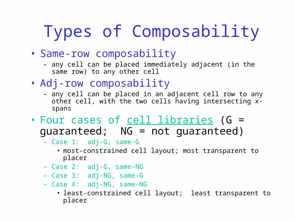
Types of Composability• Same-row composability
– any cell can be placed immediately adjacent (in the same row) to any other cell
• Adj-row composability– any cell can be placed in an adjacent cell row to any other cell, with the
two cells having intersecting x-spans
• Four cases of cell libraries (G = guaranteed; NG = not guaranteed)– Case 1: adj-G, same-G
• most-constrained cell layout; most transparent to placer– Case 2: adj-G, same-NG– Case 3: adj-NG, same-G– Case 4: adj-NG, same-NG
• least-constrained cell layout; least transparent to placer

Case 2: Adj-G, Same-NG
Blue vertices, edges = graph of phase assignment “dependencies”

Case 3: Adj-NG, Same-G
Blue vertices, edges = graph of phase assignment “dependencies”

Case 4: Adj-NG, Same-NG
Blue vertices, edges = graph of phase assignment “dependencies”

Overlap Layer Abstraction in LEF• Like “teeth of a broken comb” defined for each master cell• Placer makes sure that the teeth don’t collide when the cells are
placed, i.e., the two “broken combs” interlace• Available today in LEF standard; placer understands overlap layer
– current heuristics may not scale well if many instances have overlap geometry
Traditional picture of overlap geometries

Case 1: Adj-G, Same-G• Solution 1: “no restrictions on the cell layout”
– create cell abstractions such that placer runs in “normal” mode• e.g., pre-bloat (by 1 site) cells that have critical poly near left/right
boundary • e.g., create overlap layer obstacles corresponding to critical poly near
top/bottom boundary
• Solution 2: smart rules to restrict cell layout– e.g., every pair of boundary-CP features from the same cell must be
non-interfering• definition: two features are non-interfering if they are in different
connected components of the cell’s phase conflict graph– no boundary-CP feature is “near” two different sides of its cell– these two restrictions composability guaranteed (no odd cycles
possible)• Solution 3: dumb rules to restrict cell layout
– all cells have 250nm-wide 0-phase boundary (IBM-style AltPSM)

Notation• M = number of master cells in library
• Ci = ith master cell, i = 1, …, M
• wi = width of ith master cell, i = 1, …, M
• Vi = number of versions of the ith master cell, i = 1, …, M
• Cik = kth version of ith master cell, i = 1, …, M; k = 1, …, Vi
• N = number of movable cells in the row of interest
• Rh = hth cell in the row of interest
• Sh = master cell corresponding to hth cell in row of interest
• boundary-CP = critical poly feature “near” the cell boundary
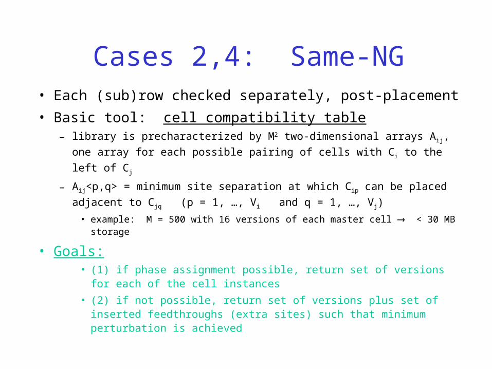
Cases 2,4: Same-NG• Each (sub)row checked separately, post-placement
• Basic tool: cell compatibility table– library is precharacterized by M2 two-dimensional arrays Aij, one array for
each possible pairing of cells with Ci to the left of Cj
– Aij<p,q> = minimum site separation at which Cip can be placed adjacent to
Cjq (p = 1, …, Vi and q = 1, …, Vj)
• example: M = 500 with 16 versions of each master cell < 30 MB storage
• Goals:• (1) if phase assignment possible, return set of versions for each of the
cell instances
• (2) if not possible, return set of versions plus set of inserted feedthroughs (extra sites) such that minimum perturbation is achieved

Cases 2,4: Same-NG Example Sol’n• Shortest-path finding in a simple graph (actually, a DAG) :
– for each version j of each cell Ri, create node <Ri,j>, i = 1, …, N and j = 1, …, Vri
– create source node <R0,0> and termination node <RN+1,0>
– create directed edges (<Ri,j>,<Ri+1,k>) for all versions j of cell Ri and versions k of cell Ri+1 (weight = cost of perturbing placement to achieve minimum allowed site separation)
– create zero-weight directed edges (<R0,0>,<R1,j>) for all versions j of cell R1 and (<RN,j>, <RN+1,0>) for all versions j of cell RN
• Minimum-perturbation solution (specifies compatible versions as well as required changes in cell positions) given by shortest path from <R0,0> to <RN+1,0>

Cases 3,4: Adj-NG Example Sol’ns
• Basic cause of problem: horizontal poly near shared rails
– complex cells that push the cell height (#pitches), e.g., latch/FF, adder, mux
• Solution 1: partial amelioration by layout constraints
– e.g., for horizontal critical poly near power rail, the outside shifter must be 0-phase (NTI style)
– can be done silently by version compatibility, etc.
• Solution 2: abstract w/existing LEF overlap layer construct

Conclusions (again)• New problem formulations
– PSM: layout practices, automated full-chip and standard-cell compatible solutions
– OPC: taxonomy of local phenomena, data reduction– function-driven corrections (can filter complexity)– hierarchy, data volume, reuse concerns
• New tool integrations– compaction, on-the-fly cell synthesis, incremental detailed routing– graph-based (verification-type) layout analyses– new performance opts, even logic opts
• Non-trivial flow, methodology effects span library creation to auto-P&R, performance optimization, etc.