Embed Size (px)
Citation preview
SUPERCONDUCTIVITY AND LOW TEMPERATURE PROPERTIES OF
NIOBIUM DISELENIDE SINGLE CRYSTALS GROWN BY DIRECT VAPOR TRANSPORT
by
Norris Earl Lewis
Dissertation submitted to the Graduate Faculty of the
Virginia Polytechnic Institute and State University
in partial fulfillment of the requirements for the degree of
DOCTOR OF PHILOSOPHY
in
MATERIALS ENGINEERING SCIENCE
APPROVED:
Dr. T. E. Leinhardt, Chairman
Dr. D. K. Anderson
Dr. J. G. Dillard
Dr. C.R. Houska
May, 1976
Blacksburg, Virginia
Dr. K. L. Reifsnider
Dr. R. F. Tipsword
Dr. J.P. Wightman
ACKNOWLEDGMENTS
I would like to dedicate this dissertation to my wife, Judy, and my
family. The patience and love they have shown and the inspiration and
help they have given throughout the past five years has contributed im-
measurably to the success of this work.
I wish to express my appreciation for the direction provided by my
graduate committee: Dr. T. E. Leinhardt, Chairman; Dr. D. K. Anderson,
Dr. J. G. Dillard, Dr. C.R. Houska, Dr. R. F. Tipsword, Dr. K. L. Reif-
snider, and Dr. J.P. Wightman. I am especially grateful to Dr. T. E.
Leinhardt for the support, direction, and assistance he has provided
throughout this work. I wish to express my appreciation to Dr. J. G.
Dillard for his assistance and direction with the many XPS measurements
that were made. The support given to me by the members of the Physics
Department, Drs. S. P. Bowen, J, R. Long, and C. D, Williams, is greatly
appreciated. Appreciation is extended to Ms. Debbie Johnson, also of the
Physics Department, who typed this manuscript.
The success of this work is in part attributed to the support faci-
lities in the Physics and Chemistry Departments. The Physics Machine
Shop staff, Luther Barnett, Melvin Shaver, Robert Ross, and John Gray
and the Physics Electronics Shop staff, Al Wyrick, John Painter, and
Grayson Wright, are gratefully acknowledged. I wish to recognize Frans
van Damme and Andy Mollick of the Glass Shop for the skillful fabrica-
tion of the glass apparatus used in this work.
I would also like to extend appreciation to the Director of Engi-
neering at Poly-Scientific, E.W. Glossbrenner, for the consideration
ii
iii
he has shown during the past five years •. I am grateful to Poly-Scienti-. fie for the experimental hardware that was provided for this work and
to the members of the Poly-Scientific staff for their helpful discussions
and assistance.
TABLE OF CONTENTS
I. INTRODUCTION ••
II. EXPERIMENTAL •
A. Crystal Nucleation and Growth . B. Crystal Preparation for Characterization . . c. X-Ray Diffraction Equipment . . . . . . D, X-Ray Photoelectron Spectroscopy Equipment . E. Low Temperature Apparatus . . . . . . . . . F. Neutron Activation Analysis . . . . . G. Apparatus and Procedure for Iodine Diffusion H. Tunnel Junction Fabrication and Equipment .
. . . . . . . . . . . . . . . . . . . . Studies . . .
. . . . . . . . . . .
Page
1
9
9 10 13 14 16 18 21 23
III. RESULTS AND DISCUSSION • • • • 2 7
A,
B.
c.
Crystal Nucleation and Growth
Crystal Characterization
1. X-Ray Diffraction ••• 2. X-Ray Photoelectron Spectroscopy
Low Temperature Measurements •
1.
2.
3.
4.
The Dependence of Critical Current Density on Crystal Thickness •.•••••••••• Superconducting Transitio.n Temperatures and Chemical Composition ••.••••••••••• The Effect of Iodine on Low Temperature Transport Properties . . . . . . . . • . • • Tunneling Measurements •••••••••••
IV. CONCLUSIONS
v.
VI.
A. Summary B. Reconnnendations For Future Work
REFERENCES.
VITA • • • •
iv
• 27
• 31
• 31 • •• 36
• • • 49
• 53
• 55
• 58 • 69
77
• • 77 79
• 81
, 84
LIST OF FIGURES
Figure
1. Structure of 2H-NbSe2 and 4H-NbSe2 (After Wilson and Yoffe 1) . . . . . . . . . . . . . . . . . . . . .
2. Multiprobe Sample Holder for Low Temperature Measure-
3.
4.
5.
ments • • • • • •
Cryostat for Low Temperature Measurements
Circuit for Measuring Transition Temperature, Transi-tion Temperature Versus Current Density, an.d Residual Resistivity Ratio • • • • • • • • • • • • • • • . • •
Versus Voltage Charac-(After J. G. Adler and
Page
2
• 17
• • 19
• 20
Circuit for Measuring Current teristics of Tunnel Junctions
29 J. E. Jackson ). • • • • 26
6. (a) Appearance of DVT 3 (NbSe2) and DVT 4 (Nb. 97se 2)
Batches; (b) Appearance of Several DVT Batches Showing Effect of Selenium Concentration on Growth Conditions •
7. Back-reflection Laue Photographs of DVT 2B and IVT lC
. 29
Crystals (3-cm crystal-to-film distance) ••••••••••• 33
8. Transmission Laue Photographs of Sections of DVT lC (a) Point Near Edge of Crystal; (b) Midpoint of Crystal (3-cm crystal-to-film distance) • • • • • • • • • • • • • 34
9. Transmission Laue Photographs of Sections of DVT lC (a) Point Near Edge of Crystal; (b) Midpoint of Crystal (3-cm crystal-to-film distance) . • , • • • • • • • • • • • • • 35
10. Photoelectron Spectrum of Nb0 3d512 , Nb0 3d312 , 4+ 4+ Nb 3d512 , and Nb 3d312 Levels in 2H-NbSe2 • • a 11 • 37
11. Photoelectron Spectrum of Nb 4d Level in 2H-NbSe2 • • • 41
12. Photoelectron Spectrum of Nb 3d512 , Nb0 3d312 , 4+ 4+ Nb 3d512 , and Nb 3d312 Levels in 2H-NbSe2 •••••••• 42
13. Photoelectron Spectrum of Nb 4d Level in 2H-NbSe2 •• . . . . 44
V
vi
Figure Page
14. Photoelectron Spectrum of Nb0 3d512 , Nb0 3d312 , 4+ 4+ Nb 3d512 , Nb 3d312 Levels in 2H-NbSe2 •.•••••••• 46
15. Photoelectron Spectrum of Nb0 3d512 , Nb0 3d312 , 4+ 4+ Nb 3d512 , Nb 3d312 Levels in 2H-NbSe2 • • •••••• 47
16. Photoelectron Spectrum of I 3d312 Level in 2H-NbSe2 Grown by Iodine Vapor Transport • , •••••••• 48
17. Transition Temperature of 2H-NbSe2 at Different Current Densities (IVT) . . . . . . . . . . . . . . . . . . . 50
18. Transition Temperature of 2H-NbSe2 at Different Current Densities (DVT) . . . . . . . . . . . . . . . . 51
19. Effect of Thickness on Critical Current Density for Samples of 2H-Nbse 2 (DVT and IVT) ••••.••••••• 54
20. Effect of Heat Treatment in Vacuum and In Iodine Atmosphere on the Transition Temperature of NbSe2 (DVT) ••• 63
21. Electronic Band Structure for NbSe2 (After McMenamin
and Spicer 39) • • ••.••••••••• 67
22. Energy Diagrams and Current-Voltage Characteristics For Tunnel Junctions. (a) Two Metals in the Normal State Separated by a Barrier; (b) A Metal in the Normal State and a Metal in the Superconducting State
41 Separated by a Barrier. (After Giaever and Megerle ) ••. 71
23. The Relative Conductance of a Pb-MgO-Mg Sandwich as a Function of Energy, (After Giaever et ai. 42) ••• , •••. 73
24. The Reduced Energy Gap as a Function of Temperature for a DVT 2 Sample(~~ BCS Theory) ••••••••••••• 75
LIST OF TABLES
Table
I. Procedure Used For Preparing DVT Crystals ••
II.
III.
Binding Energies (eV) For Niobium in 2H-NbSe2
Binding Energies (eV) Group Vb Compounds
Page
• • • 11
• • • 38
Data From McGuire et ai. 30 •••••• • • • • • • 39
IV. Transition Temperature (T ), Residual Resistance C
Ratio (RRR), Critical Current (J ), and Thickness C
(t) Data • • • 52
V. Neutron Activation Analysis of DVT and IVT Crystals • • • 60
VI. Effect of Heat Treatment and Iodine Doping on the Transition Temperature (T) and Residual Resistance
C Ratio (RRR) of DVT Crystals ••••••••••••••••• 62
vii
I. INTRODUCTION
Considerable attention has been given to the dichalcogenides of
niobium and tantalum since the early sixties. These compounds along
with other transition metal dichalcogenides have been successfully pre-
pared and subjected to studies designed to determine the effect of
their two dimensional crystallographic structure upon their low temper-
ature electrical transport properties. Nbse2 in particular has received
considerable attention because it has the highest superconducting tran-
sition temperature among the layered-structure transition metal dichal-
cogenides. Much of the work performed on these compounds throughout the 1 sixties has been summarized by Wilson and Yoffe.
2 Revolinsky et al. have shown that seven phases exist within the
composition limits of NbSe to NbSe3• Of these seven phases more atten-
tion has been given to the 2H-Nbse2 and 4H-Nbse2 phases since they are
superconducting. The 2H-Nbse2 phase has a two-layered hexagonal struc-
ture of the NbS2 type and the 4H-Nbse2 is a four-layered hexagonal
structure of a new type. In these structures the layers consist of two
parallel anion sheets between which is a sheet of cations. In both 2H
and 4H polytypes the cations are coordinated by a trigonal prism of
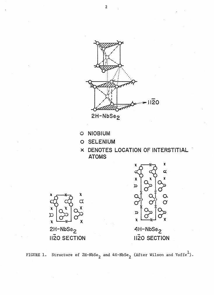
selenium anions as shown in Figure 1. The bonding between layers is
van der Waals type between anions while the bonding within the layers
is stronger and is a mixture of covalent and ionic bonds. 3 The layer
structure of this compound gives rise to anisotropic transport proper-
ties.
The possibility of studying the properties of electrons constrained
1
2
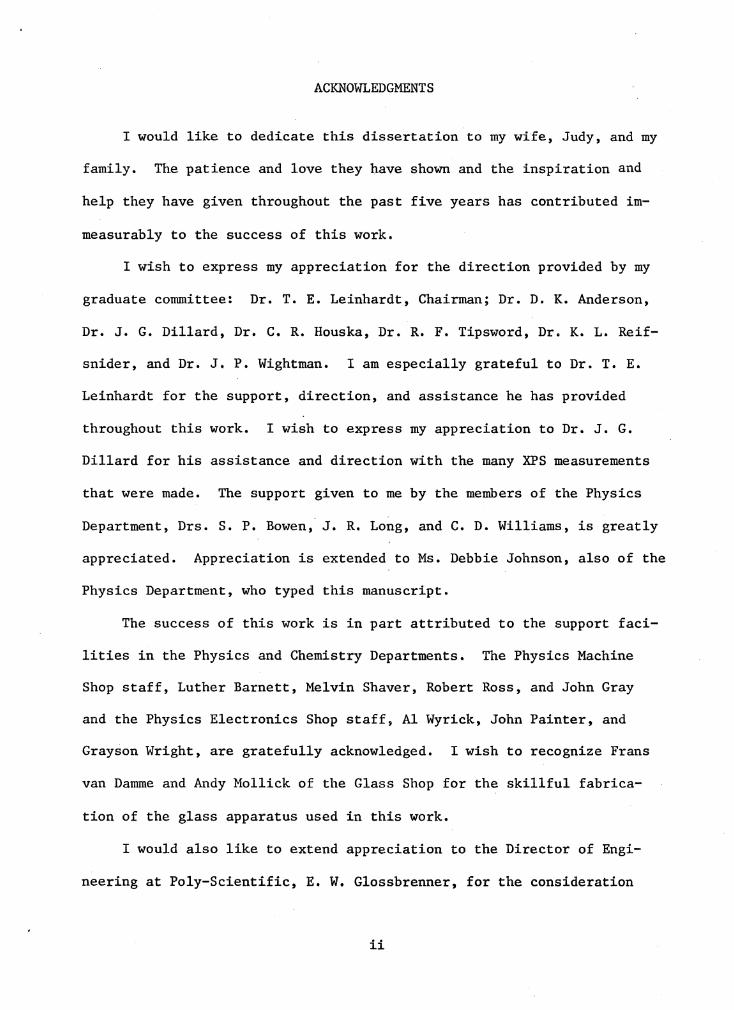
.... ~1120
2H-NbSe2
o NIOBIUM o SELENIUM x DENOTES LOCATION OF INTERSTITIAL
ATOMS
)(
C(
X ~ ~ p ~ CJ X X 2H-NbSe2 1120 SECTION
4H-NbSe2 1120 SECTION
FIGURE 1. Structure of 2H-NbSe2 and 4H-NbSe2 (After Wilson and Yoffe 1).
3
to flow in only two dimensions has been responsible for much of the
interest in the layered compounds. In addition to this, the search for
new mechanisms of superconductivity which involve interactions between
conduction electrons and organic molecules as proposed by Little 4 ,
Ginzburg 5 , and others has stimulated additional interest in these com-
pounds. The ability to insert organic molecules between the layers
(intercalation) of compounds such as Tas 2 , Nbs2 , and Nbse2 has provided
a means of constraining conduction electrons to thinner layers than
those prepared by vacuum deposition as well as placing the organic 6 mplecules in close proximity to the metallic layers. Although no evi-
dence has been found for new mechanisms of superconductivity in these
intercalation complexes, study is continuing because of the highly
anisotropic properties they possess.
In the case_of 2H-Nbse2 , studies have not been limited to the
areas of intercalation. The dependence of superconducting transition
temperatures (T) on changes in chemical composition and crystal struc-c ture has been studied 2 ' 7 • Superconducting transition temperatures were
shown to decrease from a temperature of 7°K to about 2°K in a regular
manner as the sample composition changed from Nbse2 to Nb1 •05se 2 • The
change to T was attributed to a rearrangement of the niobium sublat-c
tice, Spiering et al. 8 demonstrated that anomalies in critical current
versus magnetic field measurements were related to chemical composi-
tion. 9 .
Antonova et al. studied the effect of crystal disordering,
which resulted from changes in composition, upon superconducting criti-
cal currents.
The temperature dependence of the electrical resistivity and the

4
Hall coefficient of single crystals of 2H-NbSe2 was measured by Lee et
10 al •• The Hall coefficient was observed to undergo a change in sign at
about 26°K. Above this temperature the crystals were .E. type and below
this temperature they were n type. The Hall coefficient, magnetoresis-
tance, and thermoelectric power were measured as a function of tempera-
ture and crystal orientation by Huntley and Frindt 11 In this study a
correlation was observed between the Hall coefficient and the sample
residual resistivity ratio (RRR). The Hall coefficient was observed to
change sign at about 27°K for pure samples (high RRR) while those con-
taining larger amounts of iodine (low RRR) did not undergo a change of
sign. Yamaija et ai. 12 studied the pressure dependence of T and from C
this data concluded that the change in sign of the Hall coefficient was
caused by a crystallographic structure change.
Marezio et ai. 13 used single crystal x-ray diffraction data to
show that 2H-NbSe2 undergoes a structural distortion at 40°K. They de-
duced that the coupling of the niobium atoms is the driving mechanism
for the crystallographic distortion. 3 Thompson concluded from a sys-
tematic study of the crystal distortions that occur in Nbse 2 and other
layered compounds that a correlation exists between distortion temper-
atures and the fractional ionicity of the metal-chalcogen bond. Wilson
et aL 14 have used electron diffraction data to propose that charge
density waves, Fermi surface instabilities, occur in layered compounds
and cause the crystal distortions. It has been experimentally deter-
mined that low temperature crystallographic distortions occur in 2H-
Nbse2 which appear to explain anomalies that have been observed in
electrical properties such as the Hall coefficient and the resistivity.
5
The mechanism causing these distortions is not completely understood at
the present time.
Several experiments have been performed to determine the effect of
the anisotropic structure of 2H-Nbse2 on properties such as electrical
resistivity and the superconducting energy gap. Edwards and Frindt 15
investigated the temperature dependence of the electrical resistivity
parallel and perpendicular to the c-axis. They determined that the
ratio of the parallel and perpendicular resistivities was a constant
31:1 over the temperature range of 300 to 80°K. A linear decrease in
this ratio with temperature was observed below 80°K. Frindt et ai. 16
observed a decrease for the anisotropy in the electrical resistivity
with pressure. A value of about five was measured for the ratio of the
parallel and perpendicular resistivities at a pressure of 33 kb at
300°K.
The anisotropy of the superconducting energy gap of NbSe2 was 17 determined from far-infrared transmission spectra • The value of the
energy gap for electrons flowing parallel to the c-axis was observed
to be 1.25 meV while that for.electrons flowing perpendicular to the
c-axis was observed to be 2.15 meV at 1.6°K. Morris and Coleman18
measured the energy gap for electrons flowing parallel to the c-axis
using electron tunneling methods. The tunnel junctions studied by
these investigators were made with carbon barriers rather than metal
oxide barriers which are frequently used in tunneling experiments. An
energy gap of 1.24 meV was observed at 1.1°K. Lee et ai. 19 measured an
energy gap of 1.15 meV at 1.5°K for electrons flowing parallel to the
c-axis using a niobium point contact tunneling method.
6
The single crystals of 2H-NbSe2 used in all the areas of research
mentioned above were prepared by a chemical transport procedure that 20 21 was originally described by Schafer and Nitsche et al •• In more
22 recent years the procedure given by Kershaw et al. has been frequent-
ly used. The chemical vapor transport method involves vaporization of
the polycrystalline compound by forming a volatile chemical inter-
mediate and utilizing the temperature dependence of the chemical equi-
librium to reform the compound at a lower temperature. In the case of
2H-NbSe2 single crystals the principal transporting agent has been
iodine. The equilibrium that is involved in this case is:
+ NbSe2 + 2I 2 + NbI4 + 2Se. (1)
The formation of single crystals proceeds as follows. The chemical
intermediate, NbI4 , forms in the vaporization end of a horizontal tube
near the polycrystalline NbSe2 charge. A crystallization region of the
tube is maintained at a lower temperature. As the NbI4 and Se move
into the crystallization region, Nbse 2 reforms and deposits as single
crystals. The iodine is set free because of the temperature dependence
of NbI4 and then diffuses back to the vaporization area of the tube to
transport more NbSe2 •
The work presented here deals with the growth of single crystals
of 2H-NbSe2 by a direct vapor transport (DVT) procedure. The signi-
ficant feature of this procedure is that this material can be prepared
in a form free of the halide transporting agent. Initially it was
assumed that little, if any, transporting agent remained in the crystal 10 22 after the growth process. ' Later it was shown that significant
7
quantities of iodine can be incorporated in the lattice by th.is proce-
d 11,23,24 ure.
It has been the purpose of this work to gain an understanding of
the DVT growth mechanism and how the growth parameters affect crystal
properties. Single crystals of 2H-NbSe2 prepared by the DVT and iodine
vapor transport (IVT) procedures have been studied in a parallel
fashion. The principal impact of this work, through the availability
of DVT crystals, has been to determine the effect of iodine on the
transport properties of 2H-NbSe2 • Huntley and Frindt 11 addressed the
problem of low temperature electron scattering by iodine and structural
defects. However, in their work they did not have crystals free of
iodine and, therefore, could not completely differentiate between
structural defects induced by other means and those caused by the
presence of iodine.
The results being presented have been arranged as follows:
A. Crystal Nucleation and Growth
The effects of deviations from stoichiometery and reaction and
annealing times on DVT crystal transport properties are discussed.
B. Crystal Characterization
The results of neutron activation analysis, x-ray photoelectron
spectroscopy, and x-ray diffraction studies that were performed on both
types of crystals have been presented. The interpretation of the low
temperature transport measurem~nts have been made using these results
where possible.
C. Low Temperature Transport Measurements
Superconducting transition temperatures (T ), superconducting C
8
transition temperatures versus current densities (T vs J), critical , C
current densities versus thicknesses (J vs t), and residual resistance C
ratios (RRR) were measured for DVT and IVT crystals. The differences
observed in the properties of these samples have been explained using
the data from the literature and the ·data collected in this work.
Crystals grown by the DVT procedure were subjected to heat treat-
ment in vacuum and an iodine atmosphere. The effect upon T, J vs T C C
and RRR was measured. These observations have been interpreted in view
of other experiments designed to study the effect of impurities 11 and
structural defects 25 on the electrical transport properties of 2H-
Electron tunneling measurements were made on DVT and IVT samples
using carbon as a tunneling barrier, The results from these experi-
ments were compared to values from the literature for IVT crystals.
II. EXPERIMENTAL
A. Crystal Nucleation and Growth
All of the DVT and IVT single crystals discussed in this work were
prepared from a single lot of niobium (99.9%) and two different lots of
selenium (99.999%). These materials were purchased from the Apache
Chemicals Company. One batch of single crystals was prepared by the IVT 22 procedure described by Kershaw, et al. ·• Nine batches of single cry-
stals were prepared by the DVT procedure. These have been identified
as DVT 1, DVT 2, ••• , DVT 9. Data were taken from single crystals from
the IVT batch and seven of the nine DVT batches. The individual single
crystals taken from each of these batches have been identified as IVT
lA, IVT lB, DVT lA, DVT lC, etc., to avoid confusion when more than,one
crystal from the same batch has been characterized,
At the beginning of this effort, more emphasis was placed upon
superconductivity and other electrical transport properties than upon
nucleation and growth. After a limited number of transport measure-
ments, T , T vs J, and RRR, were made and it was discovered that the C C
RRR values of the DVT samples were higher than any IVT values published
in the literature, more emphasis was placed on growth conditions. The
growth parameters that were studied were limited to deviations from
stoichiometry, initial reaction times, times at growth temperature, and
annealing times.
The DVT method involves placing the desired quantities of Nb and
Se in quartz tubes measuring 0,15m in length by 0.02m in O.D. Prior to
-3 sealing, the tubes are evacuated to a pressure of less than 5xl0 torr
9

10
as measured with a thermocouple gauge. The tubes were then placed in a
horizontal multi-zone furnace with the charge spread evenly over the
bottom half of the tube and heated uniformly according to the procedures
outlined in Table I. Several Chromel-Alumel thermocouples were placed
along the length of each tube so that temperature uniformity could be
monitored. Temperatures were measured to within± 15°K. The total
charge weight in all cases was approximately 16 grams.
B. Crystal Preparation for Characterization
It was necessary to determine the thickness of each of the crystals
in order to calculate the current density. The current density calcu-
lated from the current flowing through the sample and the sample cros-
sectional area is an apparent current density. It is possible that all
layers of the sample may not conduct uniformly and, therefore, the real
current density may be much higher than the apparent current density.
In those instances where the crystals were thick enough (0.01 cm -
0.005 cm) the thickness was measured using an optical microscope
equipped with a filar eyepiece. The thicknesses of some of the thinner
crystals were measured with a Unitron metallograph where magnifications
greater than 25X were possible. It was necessary in some cases to cut
the crystals into rectangular shapes, the dimensions of which could be
measured accurately with a filar eyepiece. Thicknesses were then cal-
culated using crystal masses and density. The latter was determined
from lattice parameters. Huntley and Frindt 11 used a density of 6.43
g/cc calculated from lattice constants to determine the thickness of
their IVT crystals. A third means of determining the thicknesses of
the thinner crystals was to use a resistivity value which was calcu-
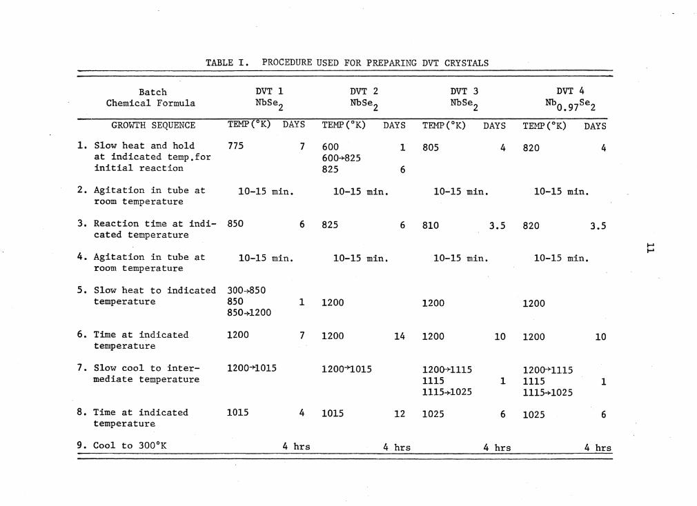
TABLE I. PROCEDURE USED FOR PREPARING DVT CRYSTALS
Batch DVT 1 DVT 2 DVT 3 DVT 4 Chemical Formula NbSe2 NbSe2 Nbse2 Nb0.97Se2
GROWTH SEQUENCE TEMP (°K) DAYS TEMP (°K) DAYS TEMP(°K) DAYS TEMP (°K) DAYS
1. Slow heat and hold 775 7 600 1 805 4 820 4 at indicated temp.for 600-+825 initial reaction 825 6
2. Agitation in tube at 10-15 min. 10-15 min. 10-15 min. 10-15 min. room temperature
3. Reaction time at indi- 850 6 825 6 810 3.5 820 3.5 cated temperature
I-' I-' 4. Agitation in tube at 10-15 min. 10-15 min. 10-15 min. 10-15 min.
room temperature
5. Slow heat to indicated 300-+850 temperature 850 1 1200 1200 1200
850+1200
6. Time at indicated 1200 7 1200 14 1200 10 1200 10 temperature
7. Slow cool to inter- 1200-+1015 1200-+1015 1200-+1115 120Q-+1115 mediate temperature 1115 1 1115 1
1115+1025 1115-+1025
8. Time at indicated 1015 4 1015 12 1025 6 1025 6 temperature
9. Cool to 300°K 4 hrs 4 hrs 4 hrs 4 hrs
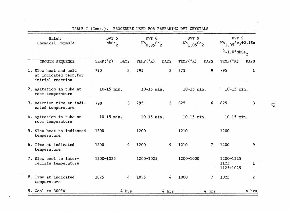
TABLE I (Cont.). PROCEDURE USED FOR PREPARING DVT CRYSTALS
Batch DVT 5 DVT 6 DVT 9 DVT 9 Chemical Formula Nbse 2 Nb0.95Se2 Nbl.05Se2 Nbl. 05se 2+0.1Se
I), -+1. 05NbSe2
GROWTH SEQUENCE TEMP(°K) DAYS TEMP(°K) DAYS TEMP(°K) DAYS TEMP (°K) DAYS
1. Slow heat and hold 790 3 795 3 775 9 795 1 at indicated temp~for initial reaction
2. Agitation in tube at 10-15 min. 10-15 min. 10-15 min. 10-15 min. room temperature
3. Reaction time at indi- 790 3 795 3 825 6 825 3 I-' cated temperature I',)
4. Agitation in tube at 10-15 min. 10-15 min. 10-15 min. 10-15 min. room temperature
5. Slow heat to indicated 1200 1200 1210 1200 temperature
6. Time at indicated 1200 9 1200 9 1210 7 1200 9 temperature
7. Slow cool to inter- 1200-+1025 1200-+1025 1200-+1000 1200-+1125 mediate temperature 1125 1
1125-+1025
8. Time at indicated 1025 4 1025 4 1000 7 1025 2 temperature
9. Cool to 300°K 4 hrs 4 hrs 4 hrs 4 hrs
13
lated for crystals thick enough to measure optically with sufficient
accuracy.
It was necessary to cleave the IVT and DVT crystals to gain infor-
mation about the oxidation state of niobium on the surface and in the
interior of the crystals. Since an inverse relationship between criti-26 cal current density and sample thickness has been observed for 2H-NbSe2
and since the IVT crystals grew much thicker than the DVT, it was neces-
sary to cleave the former to approximately the same thickness as the
DVT's so that the critical current density data could be compared on an
equal footing. The IVT crystals were cleaved perpendicular to the c-
axis by inserting a sharp blade parallel to the basal plane and peeling
away the layers with tweezers. In some instances these cleaved pieces
were used for neutron activation and analyses. The crystals that were
too thin to handle in this fashion were cleaved by pulling successive
layers away with sticky tape.
C. X-Ray Diffraction Equipment
Powder x-ray diffraction patterns were prepared using a General
Electric XRD-5 diffractometer. The diffractometer was equipped with a
nickel filtered copper K (A=l,5404 R) x-ray tube and a standard Geiger a
Mueller detector. Beam and detector slits were 1° and 0.1° respective-
ly. The output of the detector was fed into a pulse height analyzer
and from there to a linear recorder. Single crystals were attached to
the diffractometer sample holder using Apiezon L grease. This method
of mounting the sample allowed the crystals to be removed for other
studies by dissolving the grease with benzene. Powder samples were
presented to the diffractometer using tape with adhesive on both sides.
14
Back scattering and transmission Laue photographs were made of
single crystals using a Land XR-7 diffraction cassette attached to the
XRD-5 diffractometer. All transmission and back scattering photographs
were made with a crystal-to-film distance of 3.0 cm, a 0.01 cm collima-
tor, and Polaroid Type 57 film. The copper x-ray tube was operated at
25 KV and 25 ma for all photographs. Exposure times for transmission
photographs were typically 5 to 10 minutes, while the exposure times
required for back scattering photographs were 30 to 45 minutes. Single
crystals were mounted on the sample holder of the goniometer using
Apiezon L grease. In all cases the incident x-ray beam was parallel to
the crystal c-axis.
D. X-Ray Photoelectron Spectroscopy Equipment
An AEI ES-100 spectrometer was used to measure the x-ray photo-
electron spectra (XPS). The aluminum K01 , 2 line (1486,6 eV) was the
source of x-ray excitation in all cases. The equation describing the
energy of the photoelectrons ejected from the sample can be written as
(2)
' where EK is the kinetic energy of the emitted electron, hv is the x-
ray energy, Eb is the electron binding energy, ~sis the work function
of the sample and~ is a correction factor for charge build up on the
sample. In all cases discussed in this work the sample and spectro-
meter were electrically common so the~ term can be ignored. The
kinetic energy~ of the electron, which is what the spectrometer
' measures, is related to EK by the relation
15
where~ is the work function of the electron-analyzer material. Thus sp the expression for the binding energy of the electron can be written as
E = hv - E - ~ • b K sp (4)
Usually~ is empirically determined from materials such as carbon or sp gold whose binding energies are accurately known. The absolute binding
energy for the C ls 112 level of carbon in the sample was measured to be
284.2 eV. The binding energy of the Au 4f 512 and 4 f 712 levels were
determined relative to C ls 112 level of carbon and these valves were
found to be 87.1 eV and 83.4 eV, respectively. 27
Samples were presented to the spectrometer as single crystals or
as polycrystalline powders. The samples were attached directly to a
gold-plated rectangular probe which also served as a gold standard. In
the experiments where the single crystals were cleaved after the "as
grown" surfaces were characterized, the samples were attached to the
probe using a cellophane tape with adhesive on both sides. Thus single
crystals could be cleaved without being removed from the probe by using
a second piece of tape to lightly pull away surface layers. All cleav-
ing operations were performed in air. Single crystals were powdered
and dusted on double adhesive tape for the experiments requiring a
large amount of crystal surface area. All spectra were measured at -8 room temperature and a pressure of 10 torr.
A Digital Equipment Corporation PDP-8/e computer and a AE1-DS100
data system were used to control the spectrometer scanning function
16
such as energy region, number of energy levels scanned, length of scan
and output functions. The data were plotted on a Hewlett-Packard Model
2D-2AM X-Y recorder interfaced to a Digital Equipment Corporation PDP-
* 8/I computer using the MADCAP IV program. Point data were smoothed
using an 11-point parabolic least squares smoothing routine and plotted
as a line plot.
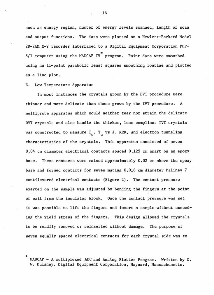
E. Low Temperature Apparatus
In most instances the crystals grown by the DVT procedure were
thinner and more delicate than those grown by the !VT procedure. A
multiprobe apparatus which would neither tear nor strain the delicate
DVT crystals and also handle the thicker, less compliant IVT crystals
was constructed to measure T, T vs J, RRR, and electron tunneling C C
characteristics of the crystals. This apparatus consisted of seven
0.04 cm diameter electrical contacts spaced 0.125 cm apart on an epoxy
base. These contacts were raised approximately 0.02 cm above the epoxy
base and formed contacts for seven mating 0.018 cm diameter Paliney 7
cantilevered electrical contacts (Figure 2). The contact pressure
exerted on the sample was adjusted by bending the fingers at the point
of exit from the insulator block. Once the contact pressure was set
it was possible to lift the fingers and insert a sample without exceed-
ing .the yield stress of the fingers. This design allowed the crystals
to be readily removed or reinserted without damage. The purpose of
seven equally spaced electrical contacts for each crystal side was to
* MADCAP= A multiplexed ADC and Analog Plotter Program. Written by G. W. Dulaney, Digital Equipment Corporation, Maynard, Massachusetts.

INSULATOR BLOCK FOR FINGERS AND CONNECTIONS TO CONTACT BASE
>
17
CHROMEL VS AU-0.07°/oFE THERMOCOUPLES
h. lcoNTACT BASE
FIGURE 2. Multiprobe Sample Holder for Low Temperature Measurements.
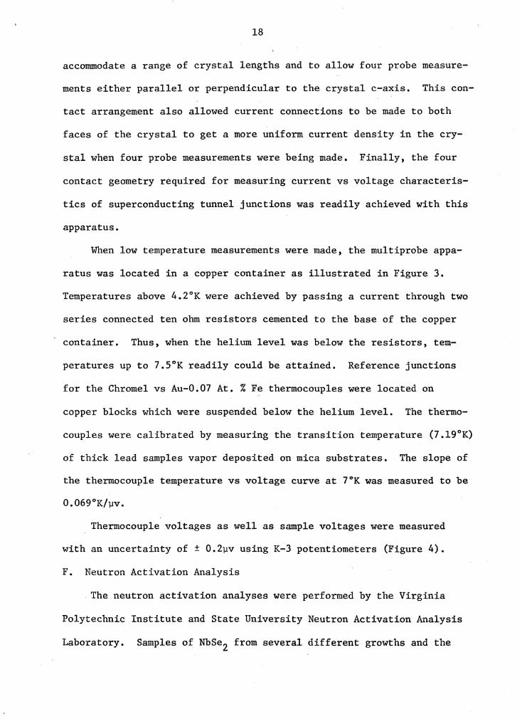
18
accommodate a range of crystal lengths and to allow four probe measure-
ments either parallel or perpendicular to the crystal c-axis. This con-
tact arrangement also allowed current connections to be made to both
faces of the crystal to get a more uniform current density in the cry-
stal when four probe measurements were being made. Finally, the four
contact geometry required for measuring current vs voltage characteris-
tics of superconducting tunnel junctions was readily achieved with this
apparatus.
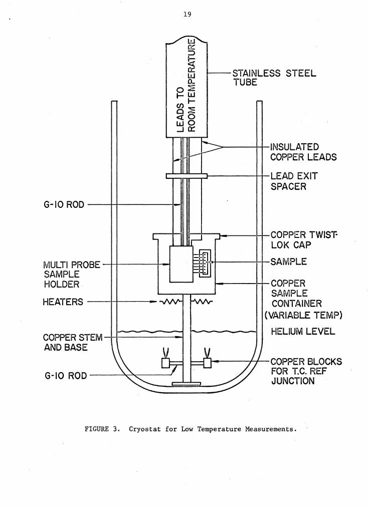
When low temperature measurements were made, the multiprobe appa-
ratus was located in a copper container as illustrated in Figure 3.
Temperatures above 4.2°K were achieved by passing a current through two
series connected ten ohm resistors cemented to the base of the copper
container. Thus, when the helium level was below the resistors, tem-
peratures up to 7.5°K readily could be attained. Reference junctions
for the Chromel vs Au-0.07 At.% Fe thermocouples were located on
copper blocks which were suspended below the helium level. The thermo-
couples were calibrated by measuring the transition temperature (7.19°K)
of thick lead samples vapor deposited on mica substrates. The slope of
the thermocouple temperature vs voltage curve at 7°K was measured to be
0.069°K/µv.
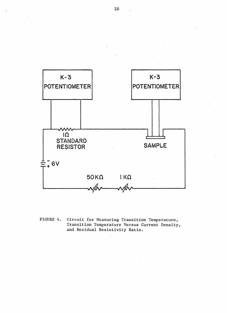
Thermocouple voltages as well as sample voltages were measured
with an uncertainty of± 0.2µv using K-3 potentiometers (Figure 4).
F. Neutron Activation Analysis
The neutron activation analyses were performed by the Virginia
Polytechnic Institute and State University Neutron Activation Analysis
Laboratory. Samples of NbSe2 from several different growths and the
19
w ~ :::> !:c a: w CL
O·~ ~w (I) .,_ 0 ,E <(0 wo ..J 0::
-- STAINLESS STEEL TUBE
-::-.---'-'-INSULATED COPPER LEADS
C::::::::::::J-----H- LEAD EXIT
G-10 ROD ----+-1-----1o-i,,,
MULTIPROBE--+-1-----+--4 SAMPLE HOLDER.
HEATERS----+~---
COPPERSTEM-+-t---~-i AND BASE
SPACER
mi-1--...,_ __ W-COPPER TWIST-LOK CAP
Ll:l::~~---H-SAMPLE
.__~---COPPER SAMPLE CONTAINER
(VARIABLE TEMP)
HELIUM LEVEL
----1--1-- COPPER BLOCKS FOR T.C. REF JUNCTION
FIGURE 3. Cryostat for Low Temperature Measurements.
K-3 POTENTIOMETER
1n STANDARD RESISTOR
-=:Gv
20
50Kn I Kn
K-3 POTENTIOMETER
SAMPLE
FIGURE 4. Circuit for Measuring Transition Temperature, Transition Temperature Versus Current Density, and Residual Resistivity Ratio,
21
niobium and selenium used to prepare these samples were analyzed by ·
this method. The samples were irradiated in a thermal flux of 1.3 x 12 2 10 n/cm - sec. Neutron activation times of seconds were required to
detect iodine while times of seven hours were required for elements
such as copper, chromium, cobalt, iron, potassium, sodium, zinc, and
several others. The activity of the samples was high after the long
activation period and could not be counted for several days. When the
analysis for iodine was performed, the samples were counted within
seconds of the activation time.
Difficulty was encountered with the analysis of the NbSe2 and
selenium samples because of the Se75 isotope. This isotope has a half
life of 120 days which is the reason a long waiting period was neces-
sary before the samples could be counted. Small sample masses (2-3 mg)
were used to minimize the interference of the se 75 isotope. However,
the smaller sample mass reduced the ability to accurately measure small
quantities of elements that do not readily activate such as iron.
The sensitivity for each of the elements detected in the samples
used in this study have been listed in Table Von page 60. The error
in the measurements is about± 10 percent of the amount present. In
some cases the error in the iron measurements is± 55 percent of the
amount present.
G. Apparatus and Procedure For Iodine Diffusion Studies
The DVT single crystals and polycrystalline material which were to
be doped with iodine were placed in a 2.0 cm O.D. quartz tube, fabri-
cated with a sealing constriction and attached to a glass manifold with
a ground glass joint. This manifold was connected to a glass and tef-
22
lon valve which served as an isolation valve from the vacuum line. The
iodine was contained in a small bulb having a volume of 2-3 cm3 which
was connected to the manifold with a side arm and a glass and teflon
valve. The valves were arranged so that the single crystals and poly-
crystalline charge could be degassed as long as desired while the bulb
containing the iodine was held at atmospheric pressure. After the de-
gassing operation was completed, the bulb containing the iodine was
evacuated to a pressure of 10 microns and held there for the desired
time. The entire manifold was closed to the vacuum line while the io-
dine was sublimed into the charge area. This was accomplished by heat-
ing the bulb containing the iodine and the connecting tubing while the
charge area was held at liquid nitrogen temperature. Sublimation of
the iodine from a side arm in this manner rather than placing it in
with the charge eliminated the transfer of nonvolatile contaminants in
the iodine to the sample. After the iodine transfer was completed, the
isolation valve to the vacuum line was opened for 1-2 minutes before
the tube was sealed. The tube was removed from the manifold, placed in
a horizontal furnace, heated to a temperature of 975°K, and held there
for the desired time.
Three samples of DVT 1 powder were used in trial experiments to
determine the amount of iodine needed to obtain a concentration of 100-
600 ppm in the crystals after diffusion. Each sample of powder weighed
approximately 300 mg. The quantity of iodine placed in the bulb was
approximately 1 mg. The quantity of iodine transferred to the charge
area was determined by the length of time the bulb was evacuated prior
to the transfer step. After iodine diffusion for three days at 1000°K,
23
half of each sample was washed with carbon tetrachloride and then placed
in carbon tetrachloride for three weeks. The carbon tetrachloride was
then decanted and the powder allowed to dry. The samples as taken from
the tubes and those washed with carbon tetrachloride were analyzed for
iodine content by neutron activation analysis. The concentrations of
iodine measured for the samples taken from the tubes were 680, 150, and
665 ppm while the concentrations observed for the samples treated with
carbon tetrachloride were 630, 80, and 460 ppm. No detectable quantity
of iodine was measured for a DVT 1 sample that had not been exposed to
iodine. These results indicate significant amounts of iodine were re-
moved by the carbon tetrachloride wash and therefore had not diffused
into the bulk of the polycrystalline material.
H. Tunnel Junction Fabrication and Equipment
Tunnel junctions of the form M/C/Nbse 2 where M=Pb or Sn and C=l00-
200 R of graphite were prepared. Carbon barriers were evaporated from
an electrode arrangement that was formed from emission spectrograph
quality electrodes. In order to bring the current density required for
carbon evaporation within the current capability of the filament trans-
former, the electrodes were machined to a smaller O.D. in the contact
area. One electrode was machined with a 0.5 cm shoulder which termi-
nated in a 20° conical tip. The mating electrode had a cylindrical
cross section measuring 0.2 cm in O.D.
The electrodes were held in contact by a negator spring which ap-
plied a nearly constant force as the electrode length decreased with
carbon evaporation. Counterelectrodes of tin were evaporated from a
tungsten basket while lead electrodes were evaporated from a tantalum
24
cup heated by a tungsten filament. The carbon electrode assembly and
the tungsten filament for evaporation of lead or tin were arranged in
the vacuum chamber so that the graphite and metal counterelectrodes
could be formed without breaking the vacuum. This was achieved by plac-
ing an aluminum shield between the electrode assemblies and using a mag-
netically controlled arm to properly locate the sample over each elec-
trode assembly.
In some instances junctions were formed on the "as grown" crystal
surfaces. In other cases the NbSe2 crystals were cleaned in distilled
acetone and distilled trichlorotrifluoroethane.
When Pb/C/Au junctions were formed, the gold surfaces were etched
with a solution consisting of one part nitric acid, five parts hydro-
chloric acid, and 6 parts (v/v) water at a temperature of 315-325°K,
followed by a boil in distilled water and a trichlorotrifluoroethane
rinse.
After locating the sample on the stainless steel sample mount 8-10
-5 cm above the carbon electrode assembly and after a pressure of lxlO to
-6 lxlO torr was reached, the carbon electrodes were outgassed at a low
current of 10-20 A for approximately one to two minutes. The carbon
barrier was formed by a series of evaporation and cooling cycles which
were necessary to allow the electrode holder to cool and thus prevent
overheating the sample. After the carbon layer appeared to be of the
* proper thickness, as indicated by its color, the sample was rotated
into a position above the tungsten filament to form the metal counter-
* A carbon thickness versus color scale was established by Milkove 28
25
electrodes. A stainless steel mask which was fabricated with three
rectangular openings was located just below the sample surface. The 2 crossectional area of the openings was 0.015 cm. The alignment of the
mask between the sample and the filament was such that three counter-
electrodes could be formed within the boundaries of the carbon layer.
In some cases the samples were not large enough to form more than one
counterelectrode.
After the junctions were fabricated they were stored in a vacuum
until they were installed in the multiprobe sample holder for analysis.
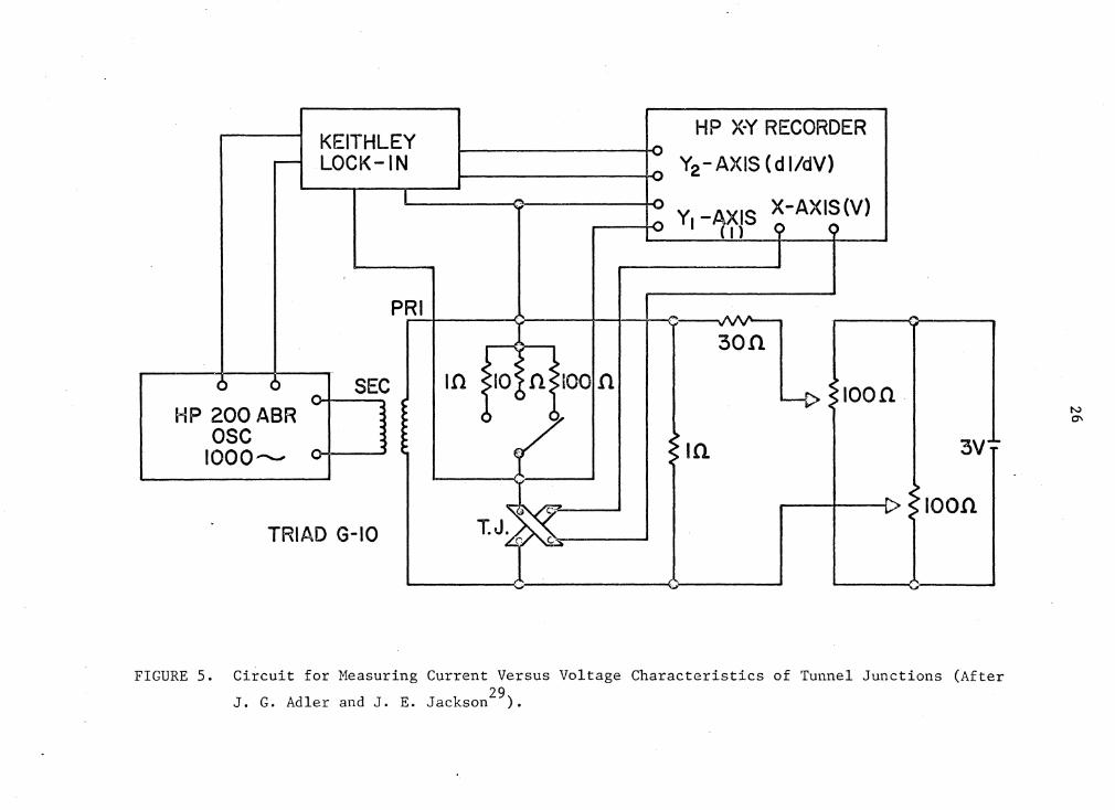
Current versus voltage and dI/dV versus voltage curves were recorded 29 for all tunnel junctions using a circuit described by Adler et al.
and shown in Figure 5.
HP 200 ABR osc
1000---
KEITHLEY LOCK-IN
PRI r-
SEC
TRIAD G-10
1n
HP X-Y RECORDER
Y2-AXIS (dl/dV)
y -AXIS X-AXIS (V) I U)
30fi
100n
10. 3V
100n
FIGURE 5. Circuit for Measuring Current Versus Voltage Characteristics of Tunnel Junctions (After 29 J. G. Adler and J. E. Jackson ).
N ~
III. RESULTS AND DISCUSSION
A. Crystal Nucleation and Growth
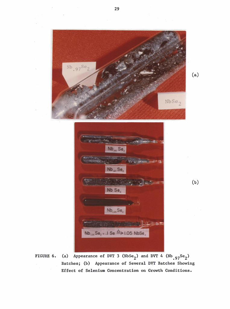
The only differences in the preparation of DVT batches 1 and 2 were
in the total time at 1200°K and in the anneal time at 1015°K. Varia-
tions in these times did not appear to affect the crystal yield or prop-
erties. As will be seen later, the transport properties of these two
batches were very similar. In both cases the resulting growths con-
sisted of masses of small single crystals intergrown and forming a cake
throughout the bottom half of the tube with several larger platelet
single crystals randomly distributed on top of the cake. Some crystals
were observed to be growing suspended from the top of the tube and com-
pletely separated from the cake. The crystals were about 2xl0- 4 to
-3 6xl0 cm thick and up to 0.6 cm in length and width.
The preparation of DVT batches 3 and 4 was the first attempt to
investigate the effect of deviations from stoichiometry. In this ex-
periment DVT 3 was prepared as NbSe2 and DVT 4 as Nb0 •97se 2• Both
batches were processed at the same time and DVT 3 served as a stoich-
iometry control. The single crystal yield and appearance on the in-
terior of the tube for DVT 3 was similar to that described for DVT 1
and DVT 2. The most significant difference that readily could be ob-
served for DVT 4 was that the cake had not remained in the bottom
half of the tube but had been transported to the upper region of the
tube and in general had an expanded appearance. The single crystals
were intergrown in many cases and were crowded by the expanded charge.
Needle-like crystals were also noted which have been described in the
27
28
. 2 literature as NbSe3 • The overall appearance of DVT 3 and DVT 4 is
shown in Figure 6. The principal differences in the time-temperature
schedules for these two growths and growths DVT 1 and DVT 2 are in the
total initial reaction time at 775-825°K and the time at 775-825°K after
the first homogenization. The total time at the 775-825°K temperature
level was shortened by a total of 6.5 days for DVT 3 and DVT 4.
Growths DVT 5 and DVT 6 were a continuation of the deviation from
stoichiometry study. DVT 5, prepared as NbSe2 and intended to be a con-
trol, was processed with DVT 6 which was prepared as Nb0 •95se 2 • The
appearance of DVT 5 and the single crystal yield was much like the other
growths prepared as NbSe2 , i.e., DVT 1, DVT 2 and DVT 3. DVT 6 had an
appearance very similar to DVT 4, i.e., needle-like crystals in some
areas and an expanded charge. DVT 6 had such a low single crystal yield
that only one crystal was found that was large enough for transport
measurements.
Growths 7 and 8 were prepared as NbSe2 and Nb099se 2 , respectively.
For these batches, the initial reaction time was limited to 3 days and
the time after the first homogenization was 2 days. The time at 1200°K
was 12 days followed by a 5 day anneal at 1025°K. DVT 7 had a high sin-
gle crystal yield. The size and shape of the crystals and the location
of the charge were similar to that of DVT 3 and DVT 5. Long needle-
like crystals and expanded charge formed in DVT 8. The single crystal
yield of DVT 8 was not as great as that of DVT 7. Tran?port measure-
ments were made on previously grown samples while many of the new
growths were being prepared. From these measurements it became apparent
that the short initial reaction time and the time after first homogeni-
29
(a)
(b)
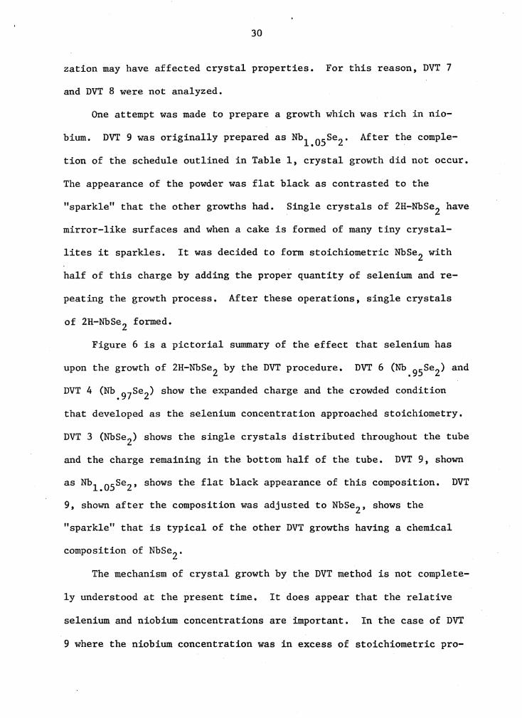
FIGURE 6. (a) Appearance of DVT 3 (Nbse 2) and DVT 4 (Nb. 97se 2) Batches; (b) Appearance of Several DVT Batches Showing Effect of Selenium Concentration on Growth Conditions.
30
zation may have affected crystal properties. For this reason, DVT 7
and DVT 8 were not analyzed.
One attempt was made to prepare a growth which was rich in nio-
bium. DVT 9 was originally prepared as Nb1 •05 se 2 • After the comple-
tion of the schedule outlined in Table 1, crystal growth did not occur.
The appearance of the powder was flat black as contrasted to the
"sparkle" that the other growths had. Single crystals of 2H-Nbse2 have
mirror-like surfaces and when a cake is formed of many tiny crystal-
lites it sparkles. It was decided to form stoichiometric Nbse 2 with
half of this charge by adding the proper quantity of selenium and re-
peating the growth process. After these operations, single crystals
of 2H-NbSe2 formed.
Figure 6 is a pictorial summary of the effect that selenium has
upon the growth of 2H-NbSe2 by the DVT procedure. DVT 6 (Nb. 95se 2) and
DVT 4 (Nb. 97se 2) show the expanded charge and the crowded condition
that developed as the selenium concentration approached stoichiometry.
DVT 3 (Nbse 2) shows the single crystals distributed throughout the tube
and the charge remaining in the bottom half of the tube. DVT 9, shown
as Nb1 •05se 2 , shows the flat black appearance of this composition. DVT
9, shown after the composition was adjusted to Nbse 2 , shows the
"sparkle" that is typical of the other DVT growths having a chemical
composition of Nbse 2 .
The mechanism of crystal growth by the DVT method is not complete-
ly understood at the present time, It does appear that the relative
selenium and niobium concentrations are important. In the case of DVT
9 where the niobium concentration was in excess of stoichiometric pro-
31
portions, growth did not occur but did occur after the proper amount of
selenium was added to the charge to bring it to stoichiometric propor-
tions. These results, when considered with the transport effects that
occurred when the selenium concentration was in excess of stoichiometry
(DVT 4 and DVT 6), indicate that selenium acts as a transporter. A
high degree of crystal perfection, as indicated by the RRR values of
133 to 140, was observed for crystals from growths DVT 1 and DVT 2. One
known difference between these and other growths which yielded crystals
with RRR values of 19 and 21 was longer initial reaction times. Longer
initial reaction times allow the selenium to be more thoroughly reacted
with the niobium and thus results in a lower selenium pressure before
the charge is taken to a higher temperature for crystal growth. 21 In the chemical transport procedure described by Nitsche et al. ,
considerable attention is placed upon m, the amount of material arriving
in the growth chamber per unit time. Nitsche indicates that whem m ex-
ceeds a critical value, the growing seeds cannot digest the arriving
materials and supersaturation will increase until additional nucleation
occurs. This can result in polynucleation and the intergrowth of cry-
stals. By analogy, it is believed that in the DVT procedure the degree
of supersaturation, which is determined by the amount of unreacted
selenium, not only determines whether growth will occur, but also de-
termines the rate of growth and the degree of crystal perfection.
B. Crystal Characterization
L X-Ray Diffraction
X-ray diffraction measurements performed on crystals from the IVT
1, DVT 1, and DVT 2 growths indicated all were in the 2H layer modifi-
32
cation. Unit cell dimensions along the C-axis were measured as 12,552
R, 12.562 R, 12.454 R, and 12.558 i for IVT lA, IVT lB, DVT lA, and DVT
2A respectively. These values are in relatively good agreement with the
value of 12.54 i given by Revolinsky et al. 2 •
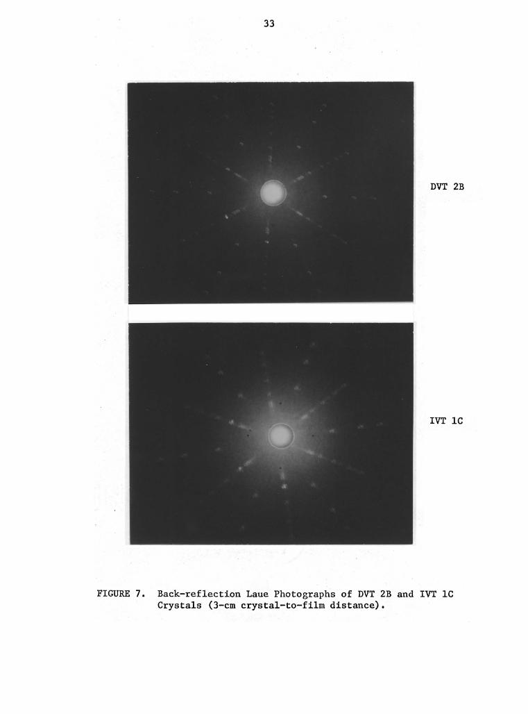
Back scattering and transmission Laue photographs were prepared for
several IVT and DVT crystals. In all cases the photographs were made
with the x-ray beam perpendicular to the basal plane. The sixfold
symmetry of the lattice for DVT lC and IVT lC crystals is readily ap-
parent from back-scattering patterns presented in Figure 7, Similar
back-scattering Laue patterns were observed for other IVT and DVT cry-
stals.
Several transmission Laue patterns were prepared to compare struc-
tural defects in both types of crystals, This analysis involved pre-
paring Laue patterns for several DVT and IVT crystals as well as pre-
paring Laue patterns for different sections of each crystal. These re-
sults are summarized in Figures 8 and 9. The amount of asterism shown
in these patterns and the variations in asterism from one section of a
crystal to another indicates structural defects are present. The elong-
ation of a Laue spot is normally associated with a crystal plane that
has been bent or otherwise distorted. IVT lC was cl.eaved from a larger
crystal and could easily have been bent during this preparation. DVT lC
was characterized "as grown", yet shows as much variation in asterism
from one section of the crystal to another as IVT lC. It is therefore
believed that some of the asterism is a 'result of layer misorientation
9 that occured during growth.· Antonova et al. associate the diffusion
and elongation of the points on Laue patterns of 2H-NbSe2 , grown by the
33
DVT 2B
IVT lC
FIGURE 7. Back-reflection Laue Photographs of DVT 2B and IVT lC Crystals (3-cm crystal-to-film distance).

34
(a)
~)
FIGURE 8. Transmission Laue Photographs of Sections of DVT lC (a) Point Near Edge of Crystal; (b) Midpoint of Crystal (3-cm crystal-to-film distance).
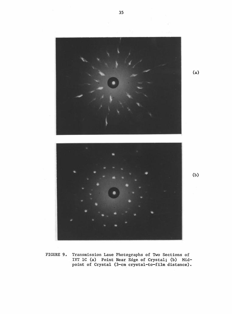
35
FIGURE 9. Transmission Laue Photographs of Two Sections of IVT lC (a) Point Near Edge of Crystal; (b) Mid-point of Crystal (3-cm crystal-to-film distance).
(a)
(b)
36
chemical vapor transport method, with a double layer misorientation re-
sulting from a shifting of layers in planes parallel to the basal plane.
The RRR values observed for DVT lC and IVT lC were 137 and 41 re-
spectively, A correlation between these values and the defect structure
shown in Figures 8 and 9 does not appear to exist, This is an indica-
tion that the RRR value for a crystal is influenced nlore by the intra-
layer structure than the interlayer structure,
2. X-Ray Photoelectron Spectroscopy
In order to characterize the surface of NbSe2 samples, core and
valence electron binding energies for niobium and selenium were
measured. XPS spectra were measured for DVT crystals representing
different transport properties and growth conditions. Data were taken
on three crystals from the IVT growth,
Measurements of the niobium core levels on the "as grown" faces
of IVT lA indicate the surface constitution is predominantly oxidized
niobium (Figure 10), The chemical composition is most likely Nbse 2
although the possibility of surface niobium oxides cannot be ruled out.
The XPS spectra reveal that the surface composition of a freshly
cleaved IVT lA is primarily elemental niobium. The identification of
Nb0 was accomplished by comparison of the binding energies of this work
30 with the value reported by McGuire et al, • The XPS data from this
work and that by McGuire et al. have been included as Tables II and III,
respectively. IVT lB and IVT lC were cleaved from larger crystals and
therefore could not be characterized "as grown". The cleaved surface
of IVT lB and IVT lC are very similar to that of IVT lA, (The spectrum
of IVT lC is not shown in Figure 10,) In cleaved IVT lB there is some
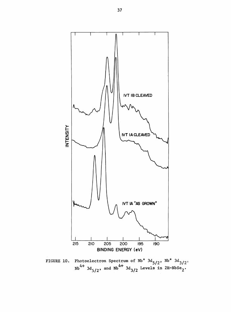
>-.... en z lLI .... z
215
37
IVT 18 CLEAVED
IVT IA 11AS GROWN"
210 205 200 195 190 BINDING ENERGY (eV)
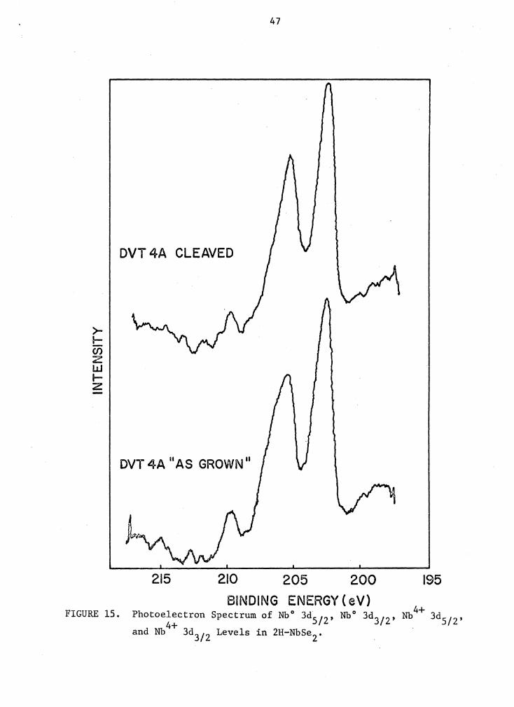
FIGURE 10. Photoelectron Spectrum of Nb0 3dS/Z' Nb0 3dJ/Z' 4+ 4+ Nb 3dS/Z' and Nb 3d312 Levels in 2H-NbSe2 •
38
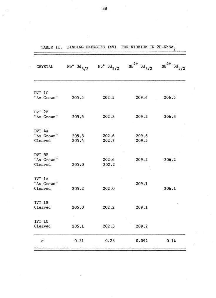
TABLE II. BINDING ENERGIES (eV) FOR NIOBIUM IN 2H-Nbse2
CRYSTAL 4+ Nb 3d3/ 2 4+
Nb 3d5/2
DVT lC "As Grown" 205.5 202.5 209.4 206.5
DVT 2B "As Grown" 205.5 202.3 209.2 206.3
DVT 4A "As Grown" 205.3 202.6 209.6 Cleaved 205.4 202.7 209.5
DVT 5B "As Grown" 202.6 209.2 206.2 Cleaved 205.0 202.2
IVT lA "As Grown" 209.1 Cleaved 205.2 202.0 206.1
IVT lB Cleaved 205.0 202.2 209.1
IVT lC Cleaved 205.1 202.3 209.2
a 0.21 0.23 0.094 0.14
39
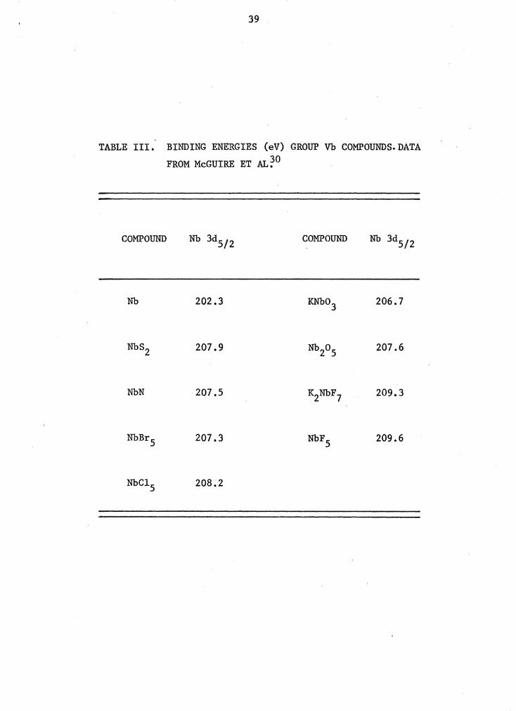
TABLE III. BINDING ENERGIES (eV) GROUP Vb CO:MPOUNDS.DATA FROM McGUIRE ET AL?O
COMPOUND COMPOUND
Nb 202.3 206.7
207.9 207.6
NbN 207.5 209.3
NbBr5 207.3 209.6
208.2
40
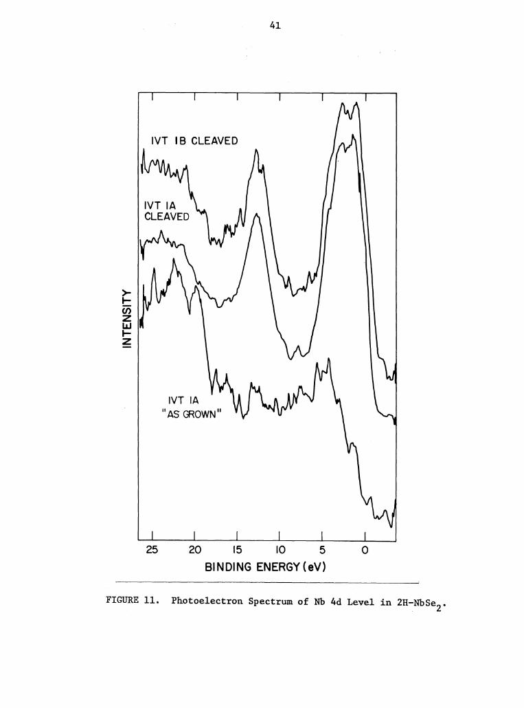
evidence of the presence of higher oxidation states of niobium as shown
by the small peak at about 209 eV and the shoulder on the Nb 3d312 peak
at about 206 eV. The appearance of the Nb 4d peak at about 14 eV in
the valence region confirms the results observed for the 190-220 eV
region (Figure 11).
The appearance of the Nb0 peak after cleaving appears to be con-
sistent with the x-ray data of Kadijk et ai. 31 which indicates that the
2H-NbSe2 structure can accommodate a considerable proportion of addi-
tional niobium atoms on octahedral interstices (See Figure 1 for struc-
ture.) However, it does not seem reasonable that there would be suf-
ficient niobium atoms on these sites to virtually screen the niobium
atoms in the Nb4+ state which are located between the selenium sheets.
Assuming that the escape depth of the ejected photoelectrons is 10-15 l, . 4+ .then it would appear that more electrons from atoms in the Nb state,
which are separated from the Nb0 atoms in the van der Waals gap by about
6 R, should have been observed. One possible interpretation of this
2 result is that the Nbl+xse 2 a phase, identified by Revolinsky et al.
is present. It was reported that the phases between NbSe and NbSe2
appear to be based on the NbSe2 structure. If this is the case, the
niobium in this compound could exist in the Nb2+ oxidation state. The
binding energies for ~ 2+ may be close to Nb0 although no data could be
found to confirm this.
An examination of the niobium core levels in the DVT lC and DVT 2B
crystals shows that both elemental niobium and oxidized niobium (NbSe2)
are present (Figure 12). The spectrum is characterized by two well
>-t-Cl) z w t-z
IVT I B CLEAVED
IVT IA CLEAVED
IVT IA 11AS GROWN"
41
25 20 15 10 5 BINDING ENERGY (eV)
0
FIGURE 11. Photoelectron Spectrum of Nb 4d Level in 2H-NbSe2 •
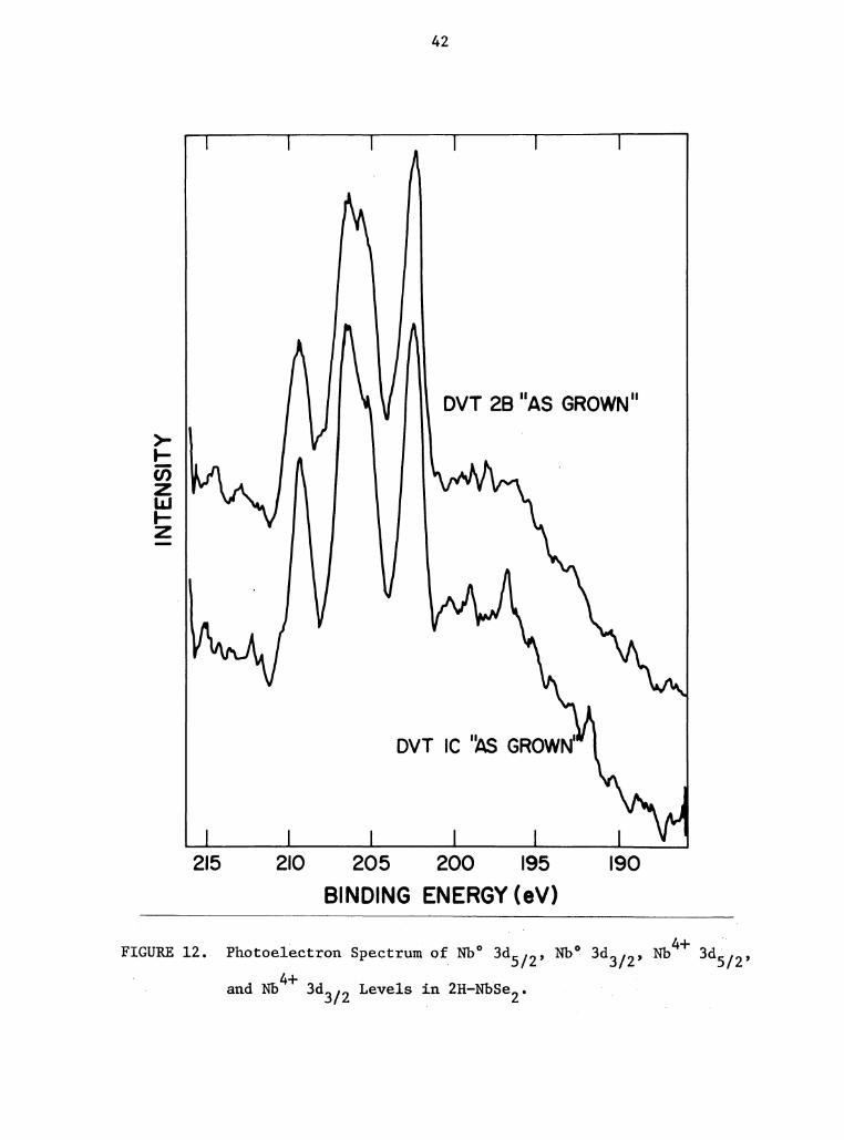
215
FIGURE 12.
42
DVT 28 11AS GROWN"
DVT IC '~ GROWN'
210 205 200 195 190 BINDING ENERGY (eV)
4+ Photoelectron Spectrum of Nb0 3d512 , Nb0 3d312 , Nb 3d512 , 4+ and Nb 3d312 Levels in 2H-NbSe2 •
43
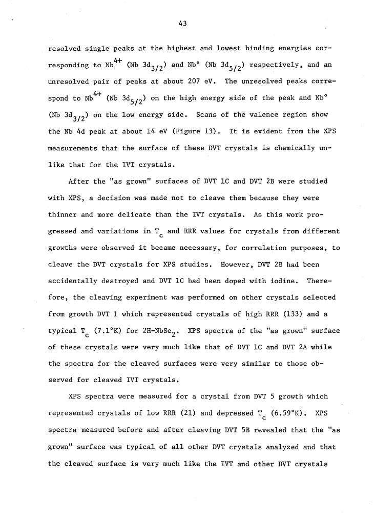
resolved single peaks at the highest and lowest binding energies cor-
responding to Nb4+ (Nb 3d312) and Nb0 (Nb 3d512 ) respectively, and an
unresolved pair of peaks at about 207 eV. The unresolved peaks corre-4+ spond to Nb (Nb 3d512 ) on the high energy side of the peak and Nb0
(Nb 3d312) on the low energy side. Scans of the valence region show
the Nb 4d peak at about 14 eV (Figure 13). It is evident from the XPS
measurements that the surface of these DVT crystals is chemically un-
like that for the IVT crystals.
After the "as grown" surfaces of DVT lC and DVT 2B were studied
with XPS, a decision was made not to cleave them because they were
thinner and more delicate than the IVT crystals. As this work pro-
gressed and variations in T and RRR values for crystals from different C
growths were observed it became necessary, for correlation purposes, to
cleave the DVT crystals for XPS studies. However, DVT 2B had been
accidentally destroyed and DVT lC had been doped with iodine. There-
fore, the cleaving experiment was performed on other crystals selected
from growth DVT 1 which represented crystals of high RRR (133) and a
typical Tc (7.1°K) for 2H-NbSe2 • XPS spectra of the "as grown" surface
of these crystals were very much like that of DVT lC and DVT 2A while
the spectra for the cleaved surfaces were very similar to those ob-
served for cleaved IVT crystals.
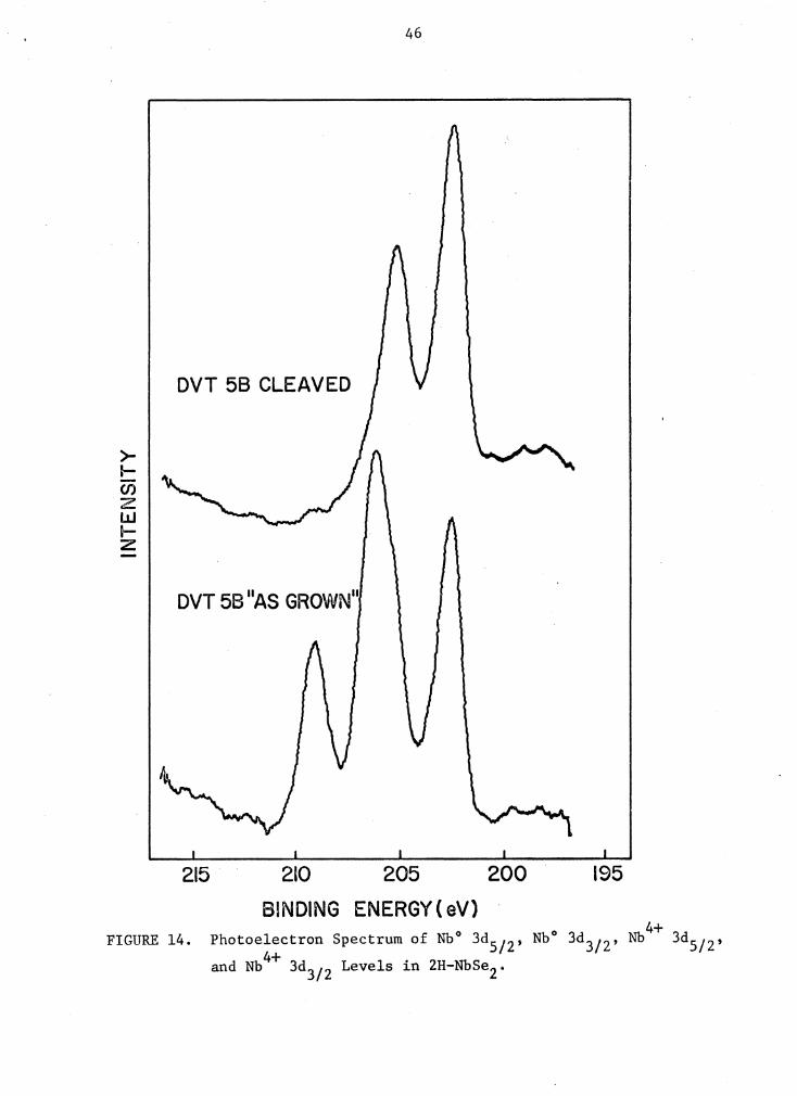
XPS spectra were measured for a crystal from DVT 5 growth which
represented crystals of low RRR (21) and depressed T (6.59°K). XPS C
spectra measured before and after cleaving DVT SB revealed that the "as
grown" surface was typical of all other DVT crystals analyzed and that
the cleaved surface is very much like the IVT and other DVT crystals
> .... Cl) z LaJ .... z
44
DVT 28 "AS GROWN"
DVT IC II AS GROWN II
25 20 15 10 5 0 BINDING ENERGY (eV)
FIGURE 13. Photoelectron Spectrum of Nb 4d Level in 2H-Nbse2•
45
(Figure 14) .
An observation that has been common to all cleaved IVT and DVT cry-
stals discussed thus far is that the cleaved surface appears to be pri-
marily elemental niobium or a very low oxidation state of niobium.
Prior to the analysis of the crystal from growth DVT 4, which is rich
in selenium, it was speculated that the niobium on the cleaved surface
would be more thoroughly oxidized by the excess selenium. The XPS 4+ 4+ spectrum for the "as grown" surface shows smaller Nb 3d312 and Nb
3d512 peaks than that observed for any of the other IVT or DVT crystals
(Figure 15). The cleaved surface is primarily elemental niobium with a
detectable quantity of the Nb4+ oxidation state. However, these peaks
do not appear to be any larger than those observed on the cleaved sur-
face of IVT 2 (Compare Figure 10 to Figure 15.) Therefore, it does not
appear that excess selenium brings about a more complete oxidation of
niobium.
Neutron activation analysis indicated the level of iodine in the
IVT crystals was 400-700 ppm. To determine the chemical form of iodine
in these crystals, the photoelectron spectrum of the iodine 3d312 level
was measured for IVT lC powder. !VT lC was chosen for this work because
it had a higher iodine content than !VT lA. !VT lC had previously been
cleaved from a larger crystal and therefore any iodine found would be
more representative of the bulk rather than an "as grown" surface. The
first XPS analysis was performed on a layer cleaved from !VT lC but no
iodine was detected. A cleaved layer was ground to increase the surface
area and the powder dusted on sticky tape. The resulting XPS spectrum
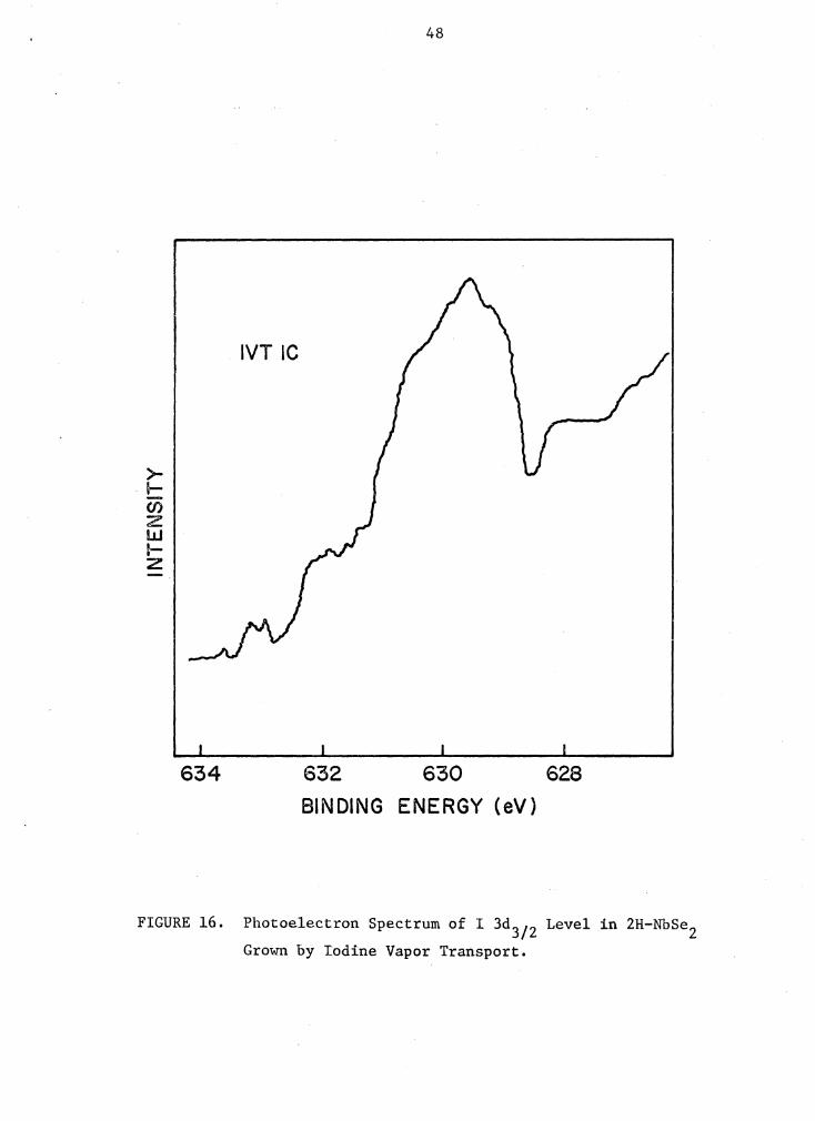
is shown in Figure 16. A binding energy of 629.6 eV was measured.
>-1-CJ) z w t-z
46
DVT 58 CLEAVED
DVT 5B 11AS GROWN"
215 210 205 BINDING ENERGY ( eV)
200 195
FIGURE 14. 4+ Photoelectron Spectrum of Nb0 3a512 , Nb0 3a312 , Nb 3a512 ,
and Nb4+ 3a312 Levels in 2H-Nbse2 •
>-1-Cl) z w ~ z
FIGURE 15.
47
DVT 4A CLEAVED
DVT 4A II AS GROWN"
215 210 205 200 195 BINDING ENERGY ( eV) 4
Photoelectron Spectrum of Nb0 3dS/Z' Nb0 3d312 , Nb+ 3dS/Z' and Nb4+ 3d312 Levels in 2H-NbSe2•
>-I-en z w t-2
48
IVT IC
634 632 630 628 BINDING ENERGY (eV)
FIGURE 16. Photoelectron Spectrum of I 3a312 Level in 2H-Nbse2 Grown by Iodine Vapor Transport,
49
This value is slightly lower than that reported for iodine in Group IIb
· d" 27 d f · · d"d 32 10 1nes an or potassium 10 1 e However, the measured binding
energy value is consistent with the existence of iodine in NbSe2 as
iodide ion. The differences between the binding energies reported here
. 27 32 and those reported earlier ' could be due to the lattice potential
at the iodide site in Nbse 2 which would affect the measured binding
32 energy
C. Low Temperature Measurements
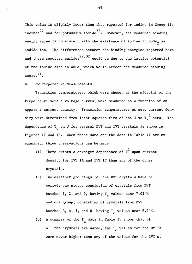
Transition temperatures, which were chosen as the midpoint of the
temperature versus voltage curves, were measured as a function of an
apparent current density. Transition temperatures at zero current den-2 sity were determined from least squares fits of the J vs T data. The
C
dependence of T on J for several DVT and IVT crystals is shown in C
Figures 17 and 18. When these data and the data in Table IV are ex-
examined, three observations can be made:
(1) 2 There exists a stronger dependence of T upon current
density for IVT lA and IVT lC than any of the other
crystals.
(2) Two distinct groupings for the DVT crystals have oc-
(3)
curred; one group, consisting of crystals from DVT
batches 1, 2, and 9, having T values near 7.05°K C
and one group, consisting of crystals from DVT
batches 3, 4, 5, and 6, having T values near 6.6°K. C
A summary of the T data in Table IV shows that of C
all the crystals evaluated, the T values for the DVT's C
were never higher than any of the values for the IVT's.
-C\I -,,; "'-u ' <C -~
170
160
150
140
130-
120
110
100
90
80
70
60
50
40
30
20
10
30
50
34 38 42 T2(0K2)
II
0
46
IVT IA
IVT IC
IVT IA-C
50 54
FLGURE 17. Transition Temperature of 2H-Nbse2 at Different Current Densities (IVT).

320
300
280
260
240
220
200
180
-160 (\J
E ~140 <( --:> 120
100
80
60
40
20
37
51
39 45
·, \
\ \
. o--o DVT IC <v--.r:;, DVT 2A 6---0 DVT 3A ~ovr 4A r!}-C DVT 5A er---o DVT 6A ~DVT 9A
\ \
47
0
49
FIGURE 18. Transition Temperature of 2H-Nbse2 at Different Current Densities (DVT).
52
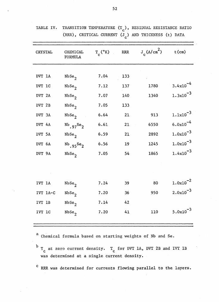
TABLE IV. TRANSITION TEMPERATURE (T ), RESIDUAL RESISTANCE RATIO C
CRYSTAL
DVT lA
DVT lC
DVT 2A
DVT 2B
DVT 3A
DVT 4A
DVT SA
DVT 6A
DVT 9A
IVT lA
IVT lA-C
IVT 1B
IVT lC
(RRR), CRITICAL CURRENT (J) AND THICKNESS (t) DATA C
CHEMICAL FORMULA
NbSe2
NbSe2
NbSe2
NbSe2
NbSe2
Nb. 97se 2
NbSe2
Nb.95Se2
NbSe2
NbSe2
NbSe2
NbSe2
NbSe2
T (°K) C
7.04
7.12
7.07
7.05
6.64
6.61
6.59
6.56
7.05
7.24
7.20
7.14
7.20
RRR
133
137
140
133
21
21
21
19
54
39
36
42
41
2 J (A/cm )
C
1780
1340
913
6550
2892
1245
1865
80
950
110
t(cm)
3 .4xl0
l.3xl0
l.lxlO
6.0xlO
l.OxlO
1.0xlO
1.4x10
1.0xlO
2.0xlO
5.0xlO
a Ch~mical formula based on starting weights of Nb and Se.
b T at zero current density. T for DVT lA, DVT 2B and IVT lB C C
was determined at a single current density.
-4
-3
-3
-4
-3
-3
-3
-2
-3
-3
c RRR was determined for currents flowing parallel to the layers.
53
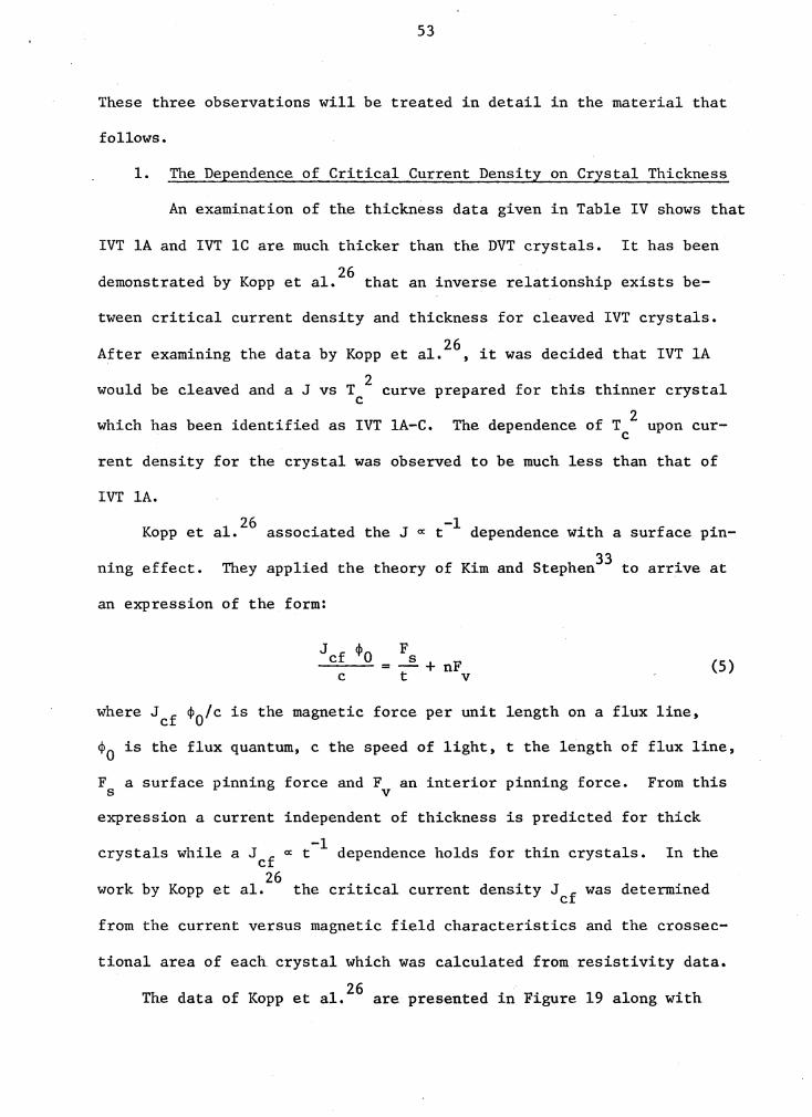
These three observations will be treated in detail in the material that
follows.
1. The Dependence of Critical Current Density on Crystal Thickness
An examination of the thickness data given in Table IV shows that
IVT lA and IVT lC are much thicker than the DVT crystals. It has been 26 demonstrated by Kopp et al. that an inverse relationship exists be-
tween critical current density and thickness for cleaved IVT crystals.
After examining the data by Kopp et ai. 26 , it was decided that IVT lA 2 would be cleaved and a J vs T curve prepared for this thinner crystal
C 2 which has been identified as IVT lA-C. The dependence of T upon cur-e
rent density for the crystal was observed to be much less than that of
IVT lA.
Kopp et al. 26 associated the J tt t-l dependence with a surface pin-
ning effect. 33 They applied the theory of Kim and Stephen to arrive at
an expression of the form:
3cf ~O F ---=~+~ C t V
where Jcf ~0/c is the magnetic force per unit length on a flux line,
(5)
~O is the flux quantum, c the speed of light, t the length of flux line,
F a surface pinning force and F an interior pinning force. From this S V
expression a current independent of thickness is predicted for thick -1 crystals while a Jcf tt t dependence holds for thin crystals. In the
26 work by Kopp et al. the critical current density Jcf was determined
from the current versus magnetic field characteristics and the crossec-
tional area of each crystal which was calculated from resistivity data.
26 The data of Kopp et al. are presented in Figure 19 along with
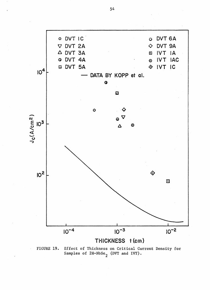
-"'
o DVT IC. V DVT 2A 6 DVT 3A 0> DVT 4A c DVT 5A
54
- DATA BY KOPP et al. (D
o DVT 6A ¢ DVT 9A l!l IVT IA 0 IVT IAC ~ IVT IC
E 103 ~ <( -0 -:,
10-3
THICKNESS t (cm) FIGURE 19. Effect of Thickness on Critical Current Density for
Samples of 2H-Nbse2 (DVT and IVT).

55
the data compiled for DVT and IVT crystals. There are basic experimen-
tal differences in the way these data were collected and therefore a
direct comparison is not intended. 26 Kopp et al. determined Jcf in the
presence of magnetic fields that ranged from 8 to 16 kOe. The critical
currents for the IVT and DVT crystals were determined in zero field and
have been defined as the current density intercept on a graph of J vs
T 2 (Figures 17 and 18). This difference explains the one or two orders C
of magnitude higher current densities observed for the DVT and IVT cry-
stals than their data. They indicated that the zero field critical cur-
rent densities for the samples they evaluated were one to two orders of
magnitude higher than those shown in Figure 19. Combining data from
DVT crystals representing different growth conditions, which could have
introduced different surface defects, along with data from IVT samples
has possibly introduced scatter in the data. Even though these dif-
ferences exist, the inverse relation with thickness can be seen in the
data. Thus the higher critical current densities observed for some of
the DVT samples are most likely related to sample thicknesses. However,
limited critical field measurements made on DVT and IVT samples have
indicated that the DVT's may possess higher Hc2 fields 34 than the IVT's.
2. Superconducting Transition Temperatures and Chemical Composition
It is believed that the grouping of the T data for the DVT sam-e
ples, the second observation, is related to growth conditions (Figure
18). As previously discussed growths DVT 1 and DVT 2 underwent longer
initial reaction times than other growths. Samples from these growths
appear to have fewer structural defects than others as evidenced by
their high RRR values. Although the growth history of DVT 9 is dif-
56
ferent than that of DVT 1 and DVT 2 it can be characterized as having a
long initial reaction time. The RRR value of 54 observed for DVT 9A
was higher than any other DVT samples with the exception of crystals
from growths DVT 1 and DVT 2. The reference to RRR values at this
point is not being made to imply that high RRR results in high T, but C
is an indicator of growth conditions. Those crystals grouped around
the T value of 6.6°K represent different growth conditions. All have C
a shorter initial reaction time than those referred to above. Ip addi-
tion to this DVT 4 and DVT 6 were prepared in a selenium rich atmosphere
which results in intergrowth between crystals and a possible higher con-
centration of defects.
When a transition temperature less than 7°K is observed for 2H-
NbSe2 it is normally attributed to a deviation from stoichiometry. This
interpretation stems from the works of Revolinsky, et al. 2 and Antonova 7 2 et al .. Revolinsky et al. have shown that as the chemical composition
goes from Nbse 2 to Nh1 _05se 2 , Tc goes from 7.0°K to about 2.2°K in a
regular manner. They report superconducting transition widths (6T) of
the order of 1-2°K for samples between the composition of Nb1 •03se 2 to
Nh1 •05se 2 • Antonova et al. 7 studied three ranges of composition: 31.7-
33.3 atomic percent (at.%) niobium (Nb_95se 2 - Nbse 2), 33.3-33.7 at.%
niobium (Nbse 2 - Nh1 •01se 2) and 33.7-34.3 at.% niobium (Nb1 •01se 2 -
Nb1 •03se 2). In the range of Nb095se 2 to Nbse 2 , this group observed that
Tc dropped from 7.0°K to 6.8°K at Nb095se 2 • This drop was associated
with the formation of vacancies in the niobium sublattice without any
change in the selenium sublattice. These results, as well as those
cited below, were obtained from x-ray line intensities from which atomic
57
scattering factors could be estimated. When the niobium content was
increased above stoichiometry (Nbse 2) no changes in Tc were observed
until a critical vacancy concentration corresponding to Nb1 •01se 2 was
reached. 7 At this concentration it was shown that niobium atoms were
being displaced from the lattice sites and a depression of T occurred. C
Transition temperatures were shown to decrease in a regular manner 7 to a value near 2°K at a composition of Nb1 •03se 2 • Transition widths
(~T) were observed to increase from a value of 0.2°K at stoichiometry
as the niobium concentration increased. Antonova et al. 7 associated an
ordering of the displaced niobium atoms, which is retained over the
range Nb1 •01se 2 to Nb1 •03se 2 , with singularities on the superconducting
transition curves and the regular behavior of these singularities with
increasing niobium concentration. Thus, it was the interpretation of
7 Antonova et al. that the rearrangement of the niobium sublattice has a
significant influence on the superconductivity of 2H-NbSe2 •
Estimates from concentration versus T data presented by Revolin-c 2 sky et al. indicate those DVT crystals grouping around the transition
temperature of 6.6°K have a composition of Nb1 •005 se 2 while the same
type of estimate from the data of Antonova et al. 7 yields a concentra-
tion of Nb1 •01se 2 • The compositional values are consistent with the ~T
values observed for all DVT samples which were <0.2°K. The difference
in the estimates from these works is related to the inabilities of these
workers to produce consistent reproducible compositions 2 . Although DVT
4A (T =6.61°K) and DVT 6A (T =6.56°K) were grown in selenium rich at-e C
mospheres they also appear to be niobium rich. The XPS data for DVT 4A
indicated excess niobium or a low oxidation state of niobium was
58
present on both the "as grown" and cleaved surfaces. The T's observed ,: c·
for these samples are below the value of 6.8°K observed by Antonova et
al. 7 for the composition of 31.7 at.% niobium (Nb_95se 2).
3. The Effect of Iodine on Low Temperature Transport Properties
An examination of the T data for the DVT's and IVT's studied C
shows the T values for the IVT's to be consistently higher than the C
values observed for the DVT samples (Table IV), The average of the four
highest DVT transition temperature values is 7.07 ± 0.02°K while the
average for all four IVT crystals studied in this work is 7.20 ± 0.02°K.
When reviewing the supporting data that was collected for these samples,
the following observations must be considered.
It has been shown that the XPS spectra for the "as grown" surfaces
of the DVT's are chemically unlike those of the IVT's, but the cleaved
surfaces of each, which should be typical of the bulk, are very similar.
Since the superconducting properties of these materials are determined
more by the bulk than the surface properties, these surface differences
do not appear to be significant. Since the same XPS spectra were ob-
served for the oxidation state of niobium in cleaved DVT and IVT samples
having T values over the range of 6.5 to 7.2°K, there does not appear C
to be a correlation with T and the XPS spectra for this energy region. C
XPS spectra were obtained for DVT and IVT crystals in the Oto 25 eV
region but the resolution was not high enough to resolve differences in
the electronic density of states near the Fermi level.
One difference that exists between these samples is the quantity
of iodine contained in the bulk. The XPS spectrum of IVT lC powder
showed iodine to be present as iodide ion. Neutron activation analysis
59
indicated the level of iodine in the IVT's is between 400 and 700· ppm
while no detectable quantity, i.e., >5 ppm could be found in the DVT's
(Table V). Other impurities were found but one of the most consistent
differences appears to be in the iodine content. To confirm that some
of the iodine was contained in bulk, a sample from IVT 1A was ground,
washed in carbon tetrachloride, and allowed to stand in carbon tetra-
chloride for three weeks. A repeat analysis of the ground portion in-
dicated 400 ppm iodine was present while 310 ppm was found in the washed
portion. (The error in these measurements is about± 10%.) Thus, it
would appear that a major portion of the iodine detected for these sam-
ples is contained in the bulk. This level is comparable to the value 23 of 100 ppm published by Myers and Monet for IVT crystals. In the work
of Huntley and Frindt 11 , up to 1.5% iodine was found in IVT crystals by
x-ray fluorescence spectroscopy. Finally, it seems quite possible that
single crystals grown at 1050°K in a container having a volume of ap-
proximately 35 cm3 and containing a 16 gram charge of polycrystalline
NbSe2 along with the recommended concentration of iodine, 5 mg per cm3
21 of container volume , could become contaminated with 400-700 ppm of
iodine.
Since the DVT's were grown without iodine, and no detectable quan-
tity of iodine could be found by neutron activation analysis in DVT
crystals, it seemed reasonable to assume that the effect of iodine on
the low temperature transport properties of 2H-NbSe2 could be deter-
mined by diffusing iodine into DVT samples. When interpreting the re-
sults from these studies, it must be realized that diffusing iodine
into a crystal after growth has occurred may not represent the same
TABLE V. NEUTRON ACTIVATION ANALYSIS OF DVT AND IVT CRYSTALS
CONTAMINANTS SENSITIVITIES (µgm) DVT la DVT 2a DVT 3b DVT Sb DVT 6b IVT lAc IVT lCc Nb Se
Co 0.14 9 7 17 20 21 4 14 14
Cr 0.34 40 104 306 440 54
Cu 0.11 19 8 61 57 64 37 116
Fe 45.0 1052 1810 3375 4900 1110 4700 1920
I 0.0026 400 670
K 0.057 76 93 116 119 55 °' Mn 0.002 58 74 129 22 14 0
Na 0.0016 272 39 184 242 191 185 186
Ta 0.088 28 13 95 79 61 4 13 262
w 0.0016 49 24 42 35 29 200 68 56
Zn 0.046 34 13 1042 730 818 50 56 26 -- -- -- -- -- -
Total (ppm) 1564 1929 5007 6357 1707 2107 5621 2648 216
RRR 133 133 21 21 19 39 41
a The results for DVT 1 and DVT 2 are based on single crystals. b The results for DVT 3, DVT 5 and DVT 6 are based on polycrystalline samples. c The results for IVT lA and IVT lC are based on pieces cleaved from these crystals.
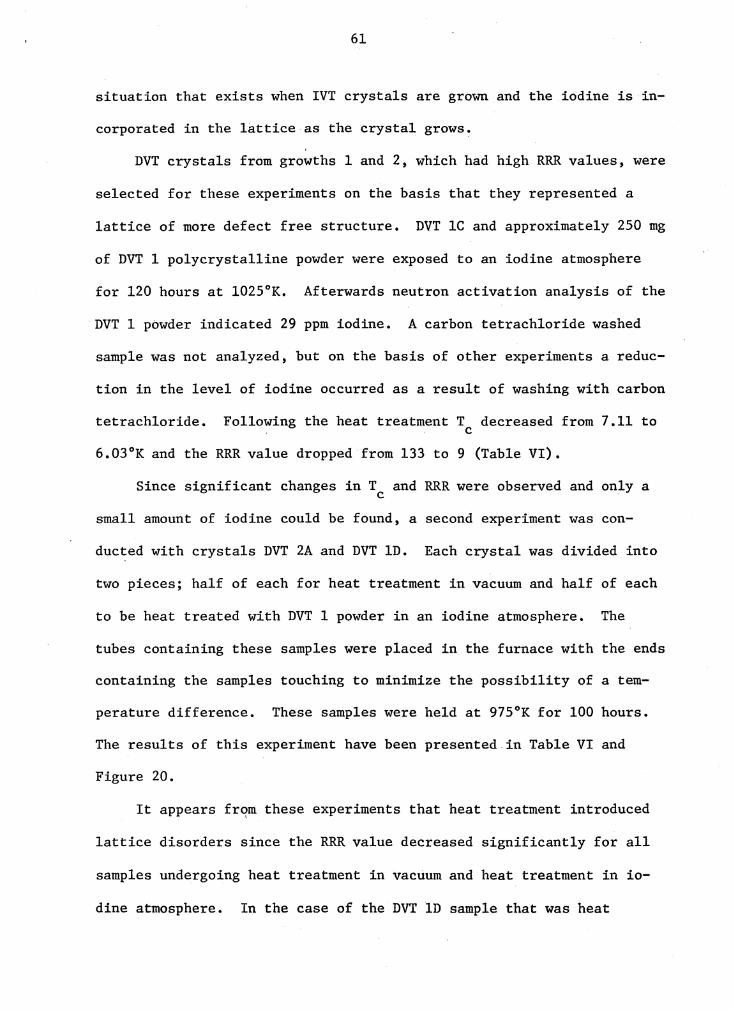
61
situation that exists when !VT crystals are grown and the iodine is in-
corporated in the lattice as the crystal grows.
DVT crystals from growths 1 and 2, which had high RRR values, were
selected for these experiments on the basis that they represented a
lattice of more defect free structure. DVT lC and approximately 250 mg
of DVT 1 polycrystalline powder were exposed to an iodine atmosphere
for 120 hours at 1025°K. Afterwards neutron activation analysis of the
DVT 1 powder indicated 29 ppm iodine. A carbon tetrachloride washed
sample was not analyzed, but on the basis of other experiments a reduc-
tion in the level of iodine occurred as a result of washing with carbon
tetrachloride. Following the heat treatment T decreased from 7.11 to C
6.03°K and the RRR value dropped from 133 to 9 (Table VI).
Since significant changes in T and RRR were observed and only a C
small amount of iodine could be found, a second experiment was con-
ducted with crystals DVT 2A and DVT lD. Each crystal was divided into
two pieces; half of each for heat treatment in vacuum and half of each
to be heat treated with DVT 1 powder in an iodine atmosphere. The
tubes containing these samples were placed in the furnace with the ends
containing the samples touching to minimize the possibility of a tem-
perature difference. These samples were held at 975°K for 100 hours.
The results of this experiment have been presented in Table VI and
Figure 20.
It appears frqm these experiments that heat treatment introduced
lattice disorders since the RRR value decreased significantly for all
samples undergoing heat treatment in vacuum and heat treatment in io-
dine atmosphere. In the case of the DVT lD sample that was heat
62
TABLE VI. EFFECT OF HEAT TREATMENT AND IODINE DOPING ON THE TRANSITION TEMPERATURE (T) AND RESIDUAL RESISTANCE
C RATIO (RRR) OF DVT CRYSTALS
DVT lC DVT lD DVT 2A
"As Grown" T (°K) 7.12 7.08 C tiT (°K) .17 .12 RRR 137 140 t(cm) -4 3.4x10 · 2.2x10 -4 1.3x10 -3
Heat Treatment In Vacuuma
TEMP (OK) 975 975 TIME (HRS.) 100 100 T (°K) b 7.09 <4.5 C ti T (°K) .10 RRR 4C 12
Heat Treatment In Iodine Atmosphere d
TEMP (OK) 1025 975 975 TIME (HRS.) 120 100 100 T (°K) 6.03 7.23 7.16 C tiT (°K) .65 .08 .25 RRR 9 21 28 Iodine (ppm) e 29 167 167
(111) (111)
a DVT lD and DVT 2A crystals were heat treated in the same tube.
b Sample was not superconducting at 4.5°K.
c RRR (300°K/4.5°K).
d DVT lD and DVT 2A crystals were heat treated in the same iodine atmosphere.
e Iodine concentration was determined by neutron activation analysis of DVT 1 powder that was in tube with crystals. Values in paren-thesis are for DVTl powder that was washed with carbon tetrachloride.

280
260
240
220
200
-180 c.\l
5160 ....... ~ 140
120
100
80
60
40
20
34
o----o DVT IC o---o DVT IC+l2 &---0 DVT 2A 8·-·-·8 DVT 2A+HT 'v--Q DVT 2A+l 2 o---0 DVT ID+l2
63
DVT ID+HT(SAMPLE WAS NOT SIC AT 4.5°K)
0
0
0
38 42
\ \ \ \ \ \ \• \ \ \ \
\ \ \ \
\~ . ~· \ \ \ .. \ \ . \
'-\ '. \ \ \ \ \ \•\
0
0
54 58
FIGURE 20. Effect of Heat Treatment in Vacuum and in Iodine Atmosphere on the Transition Temperature of 2H-NbSe2 (DVT).
64
treated in vacuum, Tc was depressed to a temperature below 4.5°K. The
reason for this depression is believed to be related to evaporation of
selenium from the lattice. In the work by Antonova et al. 7 it was re-
ported that in order to produce samples on the low selenium concentra-
tion side, a product of stoichiometric composition was annealed in a
furnace with a steep temperature gradient so that selenium could be
evaporated from the Nbse 2 lattice. A temperature gradient of 50°K over
a length of 10 cm existed while DVT lD was being heat treated. However,
a limited amount of selenium would evaporate from the lattice to de-
velop an equilibrium pressure in the tube if a temperature gradient
did not exist. Since the iodine level that existed while DVT lC was
being heat treated was low, it is possible that the prevailing mechanism
during this experiment was one of selenium evaporation from the lattice
rather than iodine diffusion into the lattice. If this were the case,
the decrease in T for DVT lC would be explained by an increase of nio-c
bium content beyond the critical composition of NbL 01se 2 •
The interpretation of the results from the heat treatment of DVT
2A appear to be more difficult. It is apparent from the drop in RRR
from 140 to 12 that disorder was introduced in the lattice yet T re-c
mained unchanged. Evaporation of selenium from the lattice should have
occurred for this sample just as it occurred with the o.thers. Since T C
did not decrease, it must be concluded that the critical composition of
Nb1 •01se 2 was not approached throughout the sample. The thickness of
DVT 2A is about six times that of DVT lD. Since the rate of selenium
evaporation is somewhat controlled by the diffusivity of selenium atoms
to the crystal surface, a thicker crystal would undergo a smaller com-
65
position change throughout per unit time than a thinner one. Thus, if
the composition of the interior of the crystal was not changed suffi-
ciently to depress T, then this region could short out the resistivity C
of the region closer to the surface. Since RRR is a property of the
normal state, the disorder that is introduced into the surface or in-
terior of the crystal will affect this property.
Neutron activation analysis of the DVT 1 powder that was heat
treated with DVT lD and DVT 2A indicated a higher concentration of io-
dine was present than that during the experiment with DVT lC. These re-
sults show that after a three week soak in carbon tetrachloride 111 ppm
iodine remained in the powder (Table VI). The T values observed for C
these crystals are higher than any observed for a DVT and are typical
of those observed for the IVT's studied in this work. The RRR values 35 36 fall within the range of 10 to 65 reported ' in the literature for
IVT samples. Thus, it appears that T has been enhanced by the C
presence of iodine.
Before attempting to explain the difference observed in T for C
IVT's and DVT's and also the changes in T resulting from iodine doping C
of DVT's, it will be necessary to discuss the parameters that affect
T. It is known from the theory of Bardeen, Cooper, and Schieffer 37 C
that the superconducting transition temperature is given by an expres-
sion of the form:
T = l.14(w} exp[-1/N(O)V] C
(6)
where (w) is a typical phonon energy, N(O) is the electronic density of
states at the Fermi surface at zero temperature and Vis the pairing
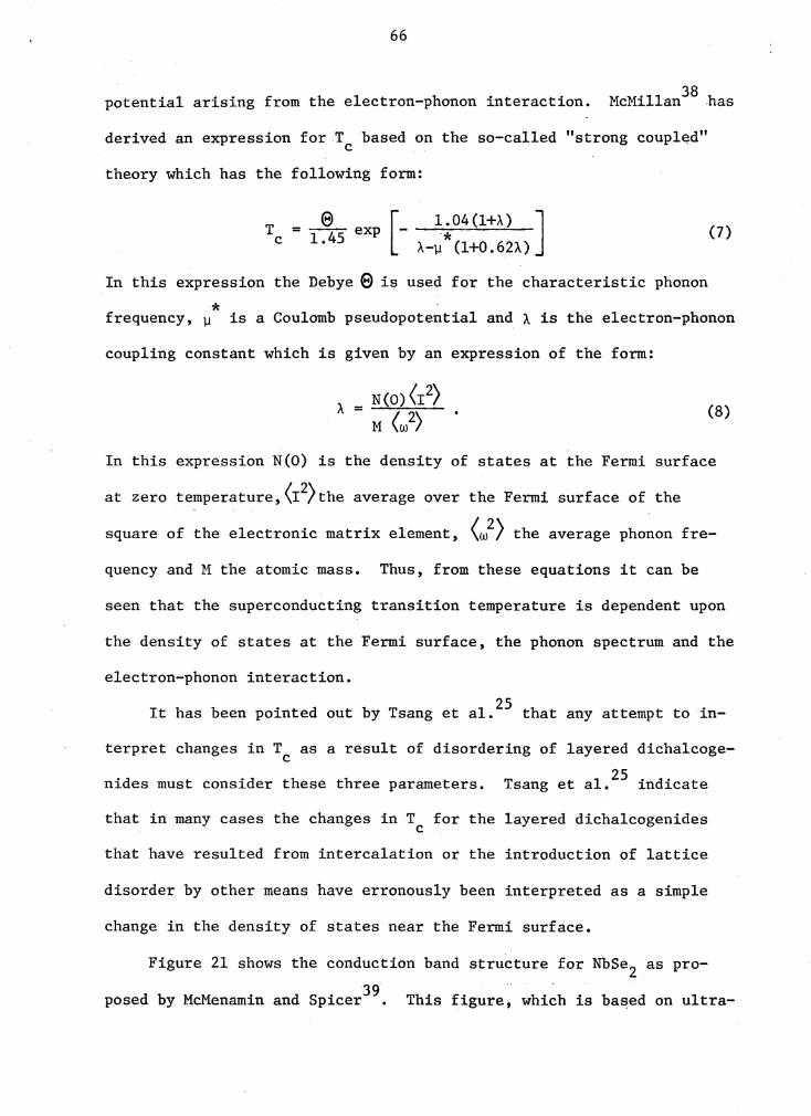
66
potential arising from the electron-phonon interaction. McMillan 38 has
derived an expression for T based on the so-called "strong coupl~d" C
theory which has the following form:
T = ~ exp [- 1.04(1+11) J c l, 45 11-µ*(1+0.62A)
In this expression the Debye E> is used for the characteristic phonon
*
(7)
frequency,µ is a Coulomb pseudopotential and A is the electron-phonon
coupling constant which is given by an expression of the form:
N(O) <r2) " = ___.. ____ _ M (w2) (8)
In this expression N(O) is the density of states at the Fermi surface
at zero temperature,(I 2)the average over the Fermi surface of the
square of the electronic matrix element, (w2) the average phonon fre-
quency and M the atomic mass. Thus, from these equations it can be
seen that the superconducting transition temperature is dependent upon
the density of states at the Fermi surface, the phonon spectrum and the
electron-phonon interaction. 25 It has been pointed out by Tsang et al. that any attempt to in-
terpret changes in T as a result of disordering of layered dichalcoge-c
nides must consider these three parameters. 25 Tsang et al. indicate
that in many cases the changes in T for the layered dichalcogenides C
that have resulted from intercalation or the introduction of lattice
disorder by other means have erronously been interpreted as a simple
change in the density of states near the Fermi surface.
Figure 21 shows the conduction band structure for NbSe2 as pro-
posed by McMenamin and Spicer 39 . This figure, which is based on ultra-
E(eV) /ri.
2-
-2-
-4-
-6-
/ I
/ /
/
--...
____ .... --' \ I _,
67
s
p
N(E) FIGURE 21. Electronic Band Structure for NbSe2 (After McMenamin
and Spicer 39).
68
violet photoelectron studies, shows the d 2 band to be partially empty z
with the Fermi level near a maximum in the electronic density of states
N(E) where N(E) is the density of states at temperatures above absolute
zero. One interpretation that has been used to explain changes in T C
of NbSe2 when it is intercalated with sodium, potassium or organic mole-
cules is that the atoms or molecules as the case may be donate a frac-
tion of an electron to the d 2 band and move the Fermi level up a small z 39 amount Since the slope of N(E) is negative at EF it decreases, and
therefore through the dependence of T upon N(E), T decreases. C C
Earlier it was shown that the XPS spectrum of IVT lC powder indi-
cated that iodine existed as iodide ion I. Therefore it is possible
that electrons were removed from the d 2 band by the iodine and thus z
N(E) increased. Since removal of electrons from the narrow d 2 band by z
iodine would bring a change of N(E) in the right direction and N(E) is
high at the Fermi level, it is possible that a very small contribution
to the difference in the T values observed for IVT samples versus DVT C
samples is related to this mechanism. If the iodine concentration were
greater than 400-700 ppm, then this mechanism could possibly account for
more of the change. This tends to place more emphasis on the dependence
of T upon changes in the phonon spectrum and the electron-phonon inter-c
action at the Fermi surface.
Perhaps the most straightforward manner to demonstrate the effect
of iodine upon the electron-phonon interaction is to consider the fol-
lowing sequence of experiments published by others.
(a) Huntley and Frindt 11 were able to eliminate the sign reversal
in the Hall coefficient that normally occurs for NbSe2 around 26°K with
69
about one percent iodine impurity.
(b) The change in sign of the Hall coefficient of NbSe2 is related 13 40 to a low temperature crystallographic structure change ' •
(c) Tsang et ai. 25 have demonstrated that electronic band structure
is sensitive to small changes in crystal structure and therefore it is
incorrect to assume that the electron-phonon interaction parameter is
independent of crystallographic changes.
This sequence of experiments indicate that small quantities of
iodine can significantly affect the crystallochemical properties of
Nbse 2 • The exact manner in which iodine brings about these changes has
not been resolved.
4. Tunneling Measurements
Tunneling measurements were included in this work to get a better
understanding of how iodine affects the electron-phonon interaction
parameter and also to extend the characterization of the DVT samples to
another area. Although these experiments were not as successful as
hoped, the results will be discussed because of their significance to
future work. A brief description of the application of electron tun-
neling measurements to study the superconducting state of a material is
given below •
. The superconducting energy gap is predicted by the theory of Bar-
deen, Cooper, and Schriefer and has been confirmed experimentally by
· specific heat, nuclear relaxation, electromagnetic absorption, and
1 1 . 41 e ectron tunne 1ng measurements • From electron tunneling measure-
ments the superconducting energy gap, the density of states at the Fer-
mi surface N(E), and in some cases information concerning the phonon
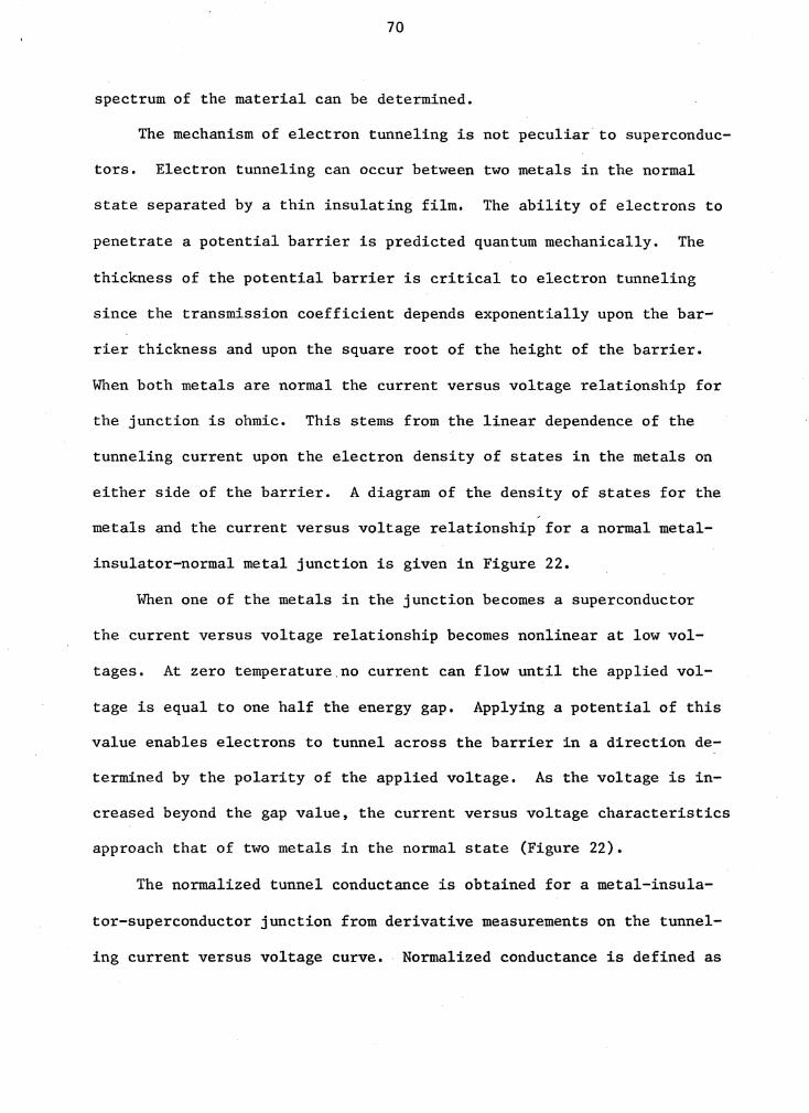
70
spectrum of the material can be determined.
The mechanism of electron tunneling is not peculiar to superconduc-
tors. Electron tunneling can occur between two metals in the normal
state separated by a thin insulating film. The ability of electrons to
penetrate a potential barrier is predicted quantum mechanically. The
thickness of the potential barrier is critical to electron tunneling
since the transmission coefficient depends exponentially upon the bar-
rier thickness and upon the square root of the height of the barrier.
When both metals are normal the current versus voltage relationship for
the junction is ohmic. This stems from the linear dependence of the
tunneling current upon the electron density of states in the metals on
either side of the barrier. A diagram of the density of states for the
metals and the current versus voltage relationship for a normal metal-
insulator-normal metal junction is given in Figure 22.
When one of the metals in the junction becomes a superconductor
the current versus voltage relationship becomes nonlinear at low vol-
tages. At zero temperature.no current can flow until the applied vol-
tage is equal to one half the energy gap. Applying a potential of this
value enables electrons to tunnel across the barrier in a direction de-
termined by the polarity of the applied voltage. As the voltage is in-
creased beyond the gap value, the current versus voltage characteristics
approach that of two metals in the normal state (Figure 22).
The normalized tunnel conductance is obtained for a metal-insula-
tor-superconductor junction from derivative measurements on the tunnel-
ing current versus voltage curve. Normalized conductance is defined as
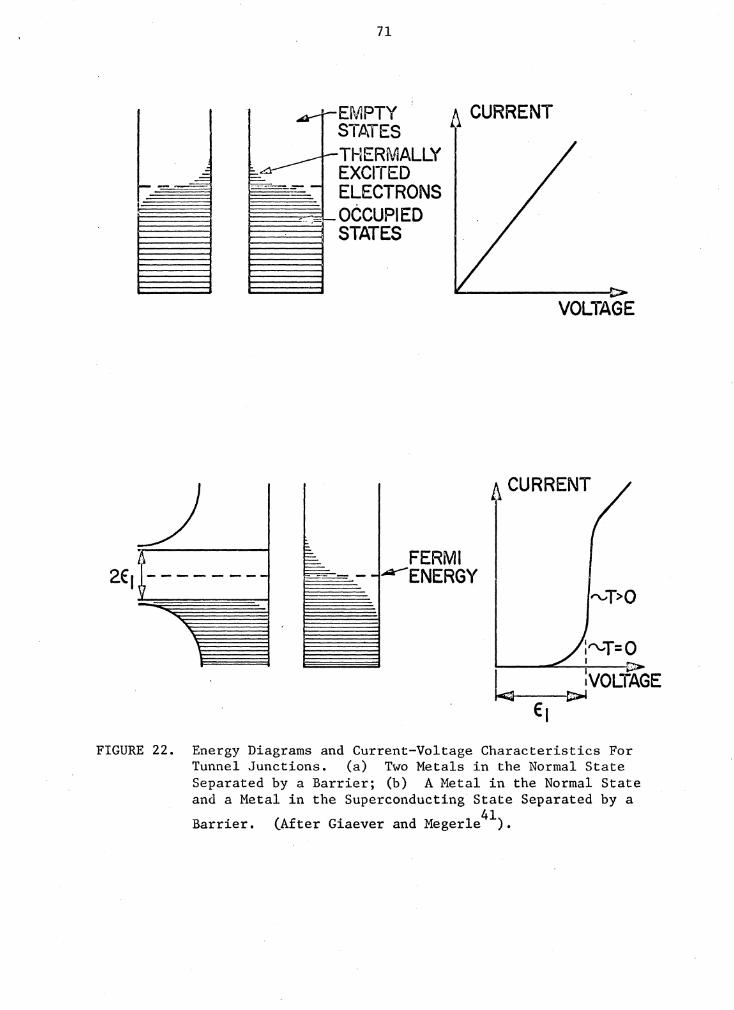
--
_) •l
2€1 - - - - - - - -,,
71
EMPTY STATES
CURRENT
THERMALLY EXCITED ELECTRONS OCCUPIED STATES
FERMI ..-ENERGY
VOLTAGE
CURRENT
rvT>O
:l"\.,T= 0 I t;>
~VOLTAGE €1
FIGURE 22. Energy Diagrams and Current-Voltage Characteristics For Tunnel Junctions. (a) Two Metals in the Normal State Separated by a Barrier; (b) A Metal in the Normal State and a Metal in the Superconducting State Separated by a Barrier. (After Giaever and Megerle 41).
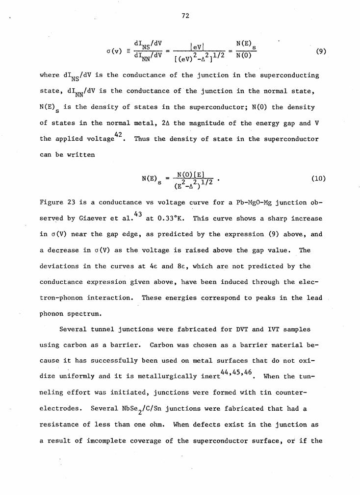
cr(v)
72
_d_rN_s_f_d_v =-_.l_e_v~l--=-N~(E_)_s - dINN/dV [(eV)2-t2]1/2 N(O)
(9)
where dINS/dV is the conductance of the junction in the superconducting
state, dINN/dV is the conductance of the junction in the normal state,
N(E) is the density of states in the superconductor; N(O) the density s
of states in the normal metal, 2t the magnitude of the energy gap and V 42 the applied voltage • Thus the density of state in the superconductor
can be written
N(E) = s (10)
Figure 23 is a conductance vs voltage curve for a Pb-MgO-Mg junction ob-
served by Giaever et ai. 43 at 0.33°K. This curve shows a sharp increase
in cr(V) near the gap edge, as predicted by the expression (9) above, and
a decrease in cr(V) as the voltage is raised above the gap value. The
deviations in the curves at 4£ and 8£, which are not predicted by the
conductance expression given above, have been induced through the elec-
tron-phonon interaction. These energies correspond to peaks in the lead
phonon spectrum.
Several tunnel junctions were fabricated for DVT and IVT samples
using carbon as a barrier. Carbon was chosen as a barrier material be-
cause it has successfully been used on metal surfaces that do not oxi-
dize uniformly and it is metallurgically inert 44 , 45 , 46 When the tun-
neling effort was initiated, junctions were formed with tin counter-
electrodes. Several Nbse 2/C/Sn junctions were fabricated that had a
resistance of less than one ohm. When defects exist in the junction as
a result of imcomplete coverage of the superconductor surface, or if the
73
4
Pb/MgO/Mg 3
2 t:= 1.34 X IQ-3eV
z T= .33° K -> ~ "CJ -' en z
2 -> "'O
' "'O -----------=------------
0 4 8 12 ENERGY ( IN UNITS OF£}
FIGURE 23. The Relative Conductance of Pb-MgO-Mg Sandwich as a
Function of Energy (After Giaever et ai. 43).
16
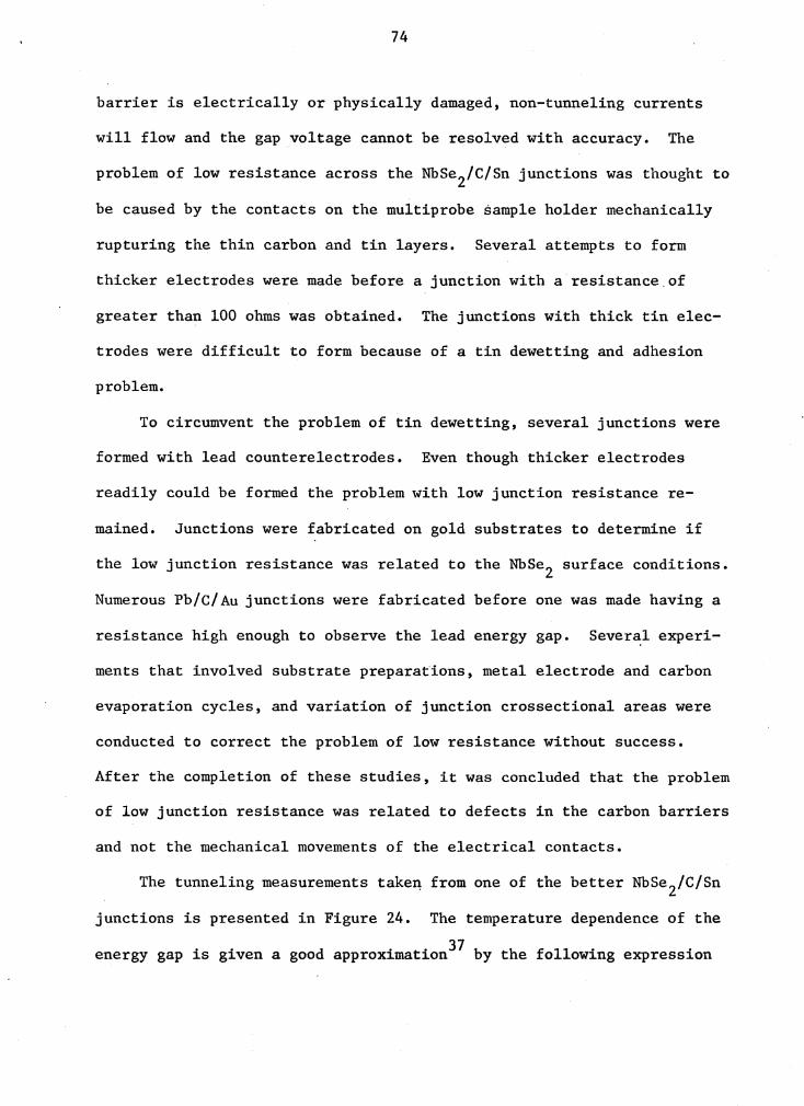
74
barrier is electrically or physically damaged, non-tunneling currents
will flow and the gap voltage cannot be resolved with accuracy. The
problem of low resistance across the Nbse 2/C/Sn junctions was thought to
be caused by the contacts on the multiprobe sample holder mechanically
rupturing the thin carbon and tin layers. Several attempts to form
thicker electrodes were made before a junction with a resistance.of
greater than 100 ohms was obtained. The junctions with thick tin elec-
trodes were difficult to form because of a tin dewetting and adhesion
problem.
To circumvent the problem of tin dewetting, several junctions were
formed with lead counterelectrodes. Even though thicker electrodes
readily could be formed the problem with low junction resistance re-
mained. Junctions were fabricated on gold substrates to determine if
the low junction resistance was related to the NbSe2 surface conditions.
Numerous Pb/C/Au junctions were fabricated before one was made having a
resistance high enough to observe the lead energy gap. Several experi-
ments that involved substrate preparations, metal electrode and carbon
evaporation cycles, and variation of junction crossectional areas were
conducted to correct the problem of low resistance without success.
After the completion of these studies, it was concluded that the problem
of low junction resistance was related to defects in the carbon barriers
and not the mechanical movements of the electrical contacts.
The tunneling measurements take~ from one of the better NbSe2/C/Sn
junctions is presented in Figure 24. The temperature dependence of the
· · d · · 3 7 b h f 11 . ' energy gap is given a goo approximation y t e o owing expression
.6(T)
.6(0)
1.0
0.5
0 0
75
NbSe2/C/Sn 6 (o)= l.26±0.2meV Tc= 7.03+ 0.02° K
.5
T Tc
1.0
FIGURE 24. The Reduced Energy Gap as a Function of Temperature for a DVT 2 Sample(~- BCS Theory).
76
!i~\ - tanh [( :c1 ( !i~n] (11)
where 2~(T) is the energy gap at temperature T and 2~(0) is the energy
gap at zero temperature. From this curve the value of ~(O) for this Dvr
2 crystal was estimated to be 1.26 ± 0.2 meV. This value is higher than
the value of 0.62 ± 0.04 meV for a NbSe/C/Pb junction reported by 36 Morris and Coleman . The energy gap in 2H-NbSe2 is known to be aniso-
tropic from infrared measurements. The value of the energy gap for
electrons flowing parallel to the layers was reported to be 1.13 mev17 •
Tunneling measurements give the value of the energy gap perpendicular to
the layers. Two possible explanations are offered for the observed
value of 1.26 ± 0.2 meV obtained by tunneling. One possibility is that
the energy gap of the DVT 2 sample is significantly higher than the IVT
samples that have previously been studied. The other possibility is
that crystal misorientation may have existed in the junction area and
the energy gap parallel to the layers rather than that perpendicular to
the layers was observed.
As a result of the high conductance observed for all of the junc-
tions made with carbon barriers and the many anomalous effects observed
in the derivatives of the current-voltage curves, attempts to study DVT
junctions as a function of iodine doping were abandoned. A more repro-
ducible means of fabricating the junction is essential.
IV. CONCLUSIONS
A. Summary
A procedure for the growth of single crystals of 2H-NbSe2 by a·
direct vapor transport (DVT) mechanism was developed. This procedure
permits high purity single crystals of this material to be grown. Re-
sidual resistance ratio values of 130 to 140 have been obtained which
are significantly higher than the values of 10 to 65 that have been re-
ported in the literature for samples prepared by the iodine vapor trans-
port (IVT) procedure. It was demonstrated that the chemical composition
of the starting material has a significant effect upon growth conditions
which in turn affects the superconducting transition temperature and
residual resistance ratio. It was concluded that selenium acts as a
transporting agent for the growth of the single crystals.
X-ray diffraction measurements were used to show that crystals
grown by direct vapor transport and iodine vapor transport procedures
have the same structure. A correlation was not found between crystal
defects, as viewed from transmission Laue patterns, and residual resis-
tance ratios.
X-ray photoelectron measurements were made of the oxidation state
of niobium on the surface and in the bulk of 2H-NbSe2 • These measure-
ments indicated the niobium on the surfaces of the IVT samples was more
completely oxidized than the niobium on the surface of the DVT samples.
X-ray photoelectron measurements indicated cleaved DVT and IVT surfaces
are similar. In both cases more niobium, which was identified as Nb0 ,
appeared to be present on the cleaved surfaces than is consistent with
77

78
the chemical formula NbSe2 and the superconducting transition tempera-
tures observed for these samples.
X-ray photoelectron spectroscopy studies were used to show that the
valence state of iodine incorporated in the lattice of the IVT samples is
consistent with the iodine existing as iodide ion. The presence of io-
dine in the IVT samples was confirmed by neutron activation analysis.
A critical current density dependence upon crystal thickness was
observed for the DVT and IVT samples. The higher critical current den-
sities that were observed for the DVT crystals were attributed primarily
to thickness. The possibility that the DVT samples may possess higher
upper critical fields (Hc2) was not discounted.
The superconducting transition temperatures of the DVT crystals with
high RRR values were observed to be about 0.1°K lower than those observed
for the IVT crystals. It was demonstrated by means of iodine doping of
the DVT crystals that the superconducting transition temperature of
2H-NbSe2 was elevated by iodine. The difference in the superconducting
transition temperatures observed for the DVT and IVT samples was attri-
buted to the presence of iodine. The mechanism by which iodine elevates
the transition temperature of 2H-Nbse 2 is not clear. It is believed
that the mechanism is more dependent upon the electron-phonon interaction
than a simple electron filling of the d band.
In conclusion the availability of single crystals of 2H-Nbse 2 free
of a halide transporting agent has allowed data regarding the supercon-
ducting state of this compound to be studied that until the present time
was not possible.
79
B. Recommendations For Future Work
A natural extension of this work would involve the preparation of
2H-Nbse 2 single crystals by the DVT procedure using higher purity nio-
bium than that used in this work, i.e. , greater than 99. 8% pure and
longer initial reaction times. The purpose of this type of study would
be to determine if RRR values above those reported in this work could
be att.ained.
Additional x-ray photoelectron spectroscopy measurements on cleaved
2H Nbs f d d . . . b. . h Nb2+ · d · - e2 sur aces an compoun s containing nio ium int e oxi ation
state would be informative. This work could provide additional informa-
tion regarding the crystallochemical nature of 2H-NbSe2 •
In view of the current interest in the relationship that exists be-
tween charge density waves, low temperature lattice distortions, and the
change in sign of the Hall coefficient at about 26°K, it may be informa-
tive to see what effects are observed when DVT crystals of high RRR are
subjected to this type of study.
Iodine doping studies at higher levels than those used in this work
performed in conjunction with transition temperature and critical field
measurements may provide additional information about the superconduct-
ing state of 2H-NbSe2•
Tunneling measurements designed to study the effect of iodine on
the electron-phonon interaction in NbSe2 appear to be desirable. How-
ever, before these studies can be performed a consistent method for
fabricating tunnel junctions will have to be developed. Junctions formed
as Al/Al 203/Al/NbSe 2 that function by the proximity effect may provide a
more consistent means for performing tunneling measurements than junc-

80
tions based on carbon barriers.
V. REFERENCES
1. J, A. Wilson and A, D. Yaffe, Adv. Phys. 18, 193 (1969).
2. E. Revolinsky, B. E. Brown, D. J. Beerntsen and C.H. Armitage, J. Less Connnon Metals.!!_, 63 (1965).
3. A.H. Thompson, Phys. Rev. Lett. 34, 520 (1975).
4. W. A. Little, Phys. Rev. 134, Al416 (1964).
5. V, L. Ginzburg, Soviet Phys. JETP Engl. Transl. 47, 2318 (1964).
6. F. R. Gamble, F. J, Di Salvo, R. A. Klennn, and T. H. Geballe, Science 168, 568 (1970).
7. A. Antonova, K. V. Kiseleva, and S. A. Medvedev, Fiz. Metallov i Metallovedenie 'l:]__, 441, (1969).
8. G. A. Spiering, E. Revolinsky, and D. J. Beerntsen, J. Phys. Chem. Solids 'l:]__, 535 (1966).
9. E. A. Antonova, S. A. Medvedev, and I. Yu Shebalin, Zh. Eksp. Teor. Fiz. ~' 329 (1969) [Sov. Phys. - JETP 30, 181 (1970)].
10. H. N. S. Lee, H. McKinzie, D. S. Tannhauser, and A. Wold, J. Appl. Phys. 40, 602 (1969).
11. D. J. Huntley and R. F. Frindt, Can. J, Phys.~' 861 (1974).
12. K. Yamaya and T. Sambongi, Solid State Connn. 11, 903 (1972).
13. M, Marezio, P. D. Dernier, A. Menth, and G. W. Hull, Jr., J. Solid State Chem.!!._, 425 (1972).
14. J. A. Wilson, F. J. Di Salvo, and S. Mahajan, Phys. Rev. Lett.~' 882 (1974).
15. J. Edwards and R. F. Frindt, J. Phys. Chem. Solids 32, 2217 (1971).
16. R. F. Frindt, R. B. Murray, G.D. Pitts, and A, D. Yaffe, J. Phys. C: Solid State Phys. 1, 154 (1972).
17. B. P. Clayman, Can. J. Phys. 50, 3193 (1972).
18. R. C. Morris and R. V. Coleman, Phys. Lett. 43A, 11 (1973).
19. D, H. Lee, L. W. Dubeck, and F. Rothwarf, Phys. Lett. 53A, 379 (1975).
81
82
20. H. Schafer, Z. Anorg. Allgem., 286 (1956).
21. R. Nitsche, H. U. Bolsterli and M. Lichtensteiger, J. Phys. Chem. Solids 21, 199 (1961).
22. R. Kershaw, M. Vlasse and A. Wold, Inorg. Chem. J!., 1599 (1967).
23. G. E. Myers and G. L. Montet, J. Phys. Chem. Solids]!, 2646 (1971).
24. N. E. Lewis, T. E. Leinhardt and J. G. Dillard, Mat. Res. Bull. 10, 967 (1975).
25. J. C. Tsang, M. W. Shafer, and B. L. Crowder, Phys. Rev. B 11, 155 (1975).
26. J, Kopp, D. J. Huntley, and R. F. Frindt, Con. J. Phys. 50, 2840 (1972).
27. R. D. Seals, R. Alexander, L. T. Taylor, and J. G. Dillard, Inorg. Chem. 12, 2485 (1973).
28. K. R. Milkove, B. S. Thesis; unpublished, M.I.T., Dept. of Physics (1975).
29. J. G. Adler and J.E. Jackson, Rev. Sci. Instru. ]I, 1049 (1966).
30. G. E. McGuire, G. K. Scheweitzer, and T. A. Carlson, Inorg. Chem. 11, 2450 (1973).
31. F. Kadijk, R. Huisman, and F. Jellinek, Rec. Trav. Chim. 83, 768 (1964).
32. C. S. Fadley, S. B. M. Hagstrom, M. P. Klein, and D. A. Shirley, J. Chem. Phys. 48, 3779 (1968).
33. Y. B. Kim and M. J. Stephen, In Superconductivity 2, edited by R. D. Parks (Marcel Dekker, Inc., New York), 1107 (1969).
34. J. R. Long, N. E. Lewis, D. Agosta, and N. K. Batra, Bull. A.P.S. 21, 291 (1976).
35. B. P. Clayman and R. F. Frindt, Solid State Comm. 2., 1881 (1971).
36. R, C. Morris, R. V. Coleman, and R. Bhandari, Phys. Rev. B 1, 895 (1972).
37. J, Bardeen, L. N. Cooper, and Schrieffer, Phys. Rev. 106, 162 (1957); 108, 1175 (1957).
38. W, L. McMillan, Phys. Rev. 167, 331 (1968).
83
39. J. C. McMenamin and W. E. Spicer, Phys. Rev. Lett. 12_, 1501 (1972).
40. J. A. Wilson, F. J. Di Salvo, and S. Mahajan, Adv. in Phys. 24, 117 (1975).
41. I. Giaever and K. Megerle, Phys, Rev. 122, 1101 (1961).
42. J. R. Schrieffer, "Tunneling Phenomena in Solids", (edited by E. Burstein and S. Lundquist), p. 287. Plenum Press, New York (1969).
43. I. Giaever, H. R. Hart, Jr., and K. Megerle, Phys. Rev. 126, 941 (1962).
44. M. L.A. Macvicar, S. M. Freake, and C. J. Adkins, J. Vac. Sc. and Tech. E_, 717 (1969).
45. M. L.A. MacVicar, J. Appl. Phys. 41, 4765 (1970).
46. S. I. Ochiai, M. L.A. Macvicar, and R. M. Rose, Phys. Rev.Bi, 2988 (1971).

The vita has been removed from the scanned document

SUPERCONDUCTIVITY AND LOW TEMPERATURE PROPERTIES OF
NIOBIUM DISELENIDE SINGLE CRYSTALS GROWN BY DIRECT VAPOR TRANSPORT
by
Norris Earl Lewis
(ABSTRACT)
A procedure for the growth of high purity single crystals of 2H-
Nbse2 by a direct vapor transport (DVT) method was developed. Single
crystal growth rate and the degree of crystal perfection were studied as
deviations from stoichiometry were made over the compositional range of
Nb0 . 95se 2 to Nb1 •05se 2 • Single crystal perfection was also studied as
changes were made in the reaction and annealing times. Residual resis-
tivity ratio (RRR) values were observed over the range of 21 to 140 and
superconductivity was observed over the range of 6.60°K to 7.12°K as
growth conditions were varied. It was concluded that selenium acts as
a transporting agent for the growth of the single crystals.
X-ray photoelectron spectroscopy (XPS) measurements were made of
the oxidation state of niobium on the surface and in the bulk of 2H-NbSe2
samples prepared by the DVT and iodine vapor transport (IVT) procedures.
These measurements indicated the niobium on the surface of the IVT sam-
ples was more completely oxidized than the niobium on the surface of
the DVT samples, whereas, XPS spectra of cleaved DVT and IVT surfaces
were similar. In both cases more niobium, which was identified as Nb0 ,
appeared to be present on the cleaved surfaces than is consistent with
the chemical formula NbSe2 and the superconducting transition tempera-
tures observed for these samples. X-ray photoelectron spectroscopy
measurements made of the 3d312 level of iodine incorporated in the lat-
tice of the IVT samples indicated the iodine is present as iodide ion.
A critical current density dependence upon crystal thickness was
observed for the DVT and IVT samples. The higher critical current den-
sities that were observed for the DVT crystals were attributed primarily
to thickness.
The superconducting transition temperatures of the DVT crystals with
the highest degree of crystal perfection were observed to be about 0.1°K
lower than those observed for the IVT crystals. It was demonstrated by
means of iodine doping of the DVT crystals that the superconducting
transition temperature of 2H-NbSe2 was elevated by iodine.


![Electronic Origin of High Temperature Superconductivity in ... · Fe-based superconductors[1]. Understanding the origin of high temperature superconductivity in such a strictly two-dimensional](https://img.pdfslide.net/doc/110x75/60273037051ec676225803a1/electronic-origin-of-high-temperature-superconductivity-in-fe-based-superconductors1.jpg)