Embed Size (px)
Citation preview
Document Number: MD00774Revision 00.01June 23, 2010
Suspending and Resuming a Single-Core MIPS-Based™ Processor for Power Saving

2 Single-Core MIPS-Based Processor Suspend/Resume Application Note, Revision 0.01
Contents
Section 1: Introduction........................................................................................................................... 31.1: Power Management Options ....................................................................................................................... 31.2: Additional Considerations for Power Management ..................................................................................... 3
Section 2: Clock Gating ......................................................................................................................... 42.1: Designs Implementing Top Level Clock Gating........................................................................................... 5
2.1.1: Instruction Controlled Clock Gating.................................................................................................... 52.1.2: Register Controlled Clock Gating....................................................................................................... 52.1.3: Reduction of VDD During Sleep Mode............................................................................................... 62.1.4: Restart Latency Trade-Offs................................................................................................................ 6
2.2: Designs Not Implementing Top Level Clock Gating .................................................................................... 62.3: Designs Implementing Fine Grain Clock Gating.......................................................................................... 7
Section 3: Power Gating ........................................................................................................................ 73.1: Hardware Suspend/Resume ....................................................................................................................... 83.2: Software Suspend/Resume......................................................................................................................... 9
3.2.1: Overview of Suspend/Resume Process............................................................................................. 93.2.2: Suspend Process ............................................................................................................................. 11
3.2.2.1: Save GPR Registers .............................................................................................................. 123.2.2.2: Save CP0 Registers ............................................................................................................... 143.2.2.3: Flush Dirty Lines in L1 Data Cache ........................................................................................ 143.2.2.4: Save the Resume Address..................................................................................................... 163.2.2.5: Copy Memory Power Down Sequence Into Cache ................................................................ 163.2.2.6: Move Memory to Low Power Mode ........................................................................................ 163.2.2.7: Shut Down Power to the MIPS Core ...................................................................................... 16
3.2.3: Resume Process.............................................................................................................................. 183.2.3.1: System Wake-Up.................................................................................................................... 183.2.3.2: Power-Up VDD to the MIPS Core and Assert Power-On Reset............................................. 183.2.3.3: Warm/Cold Boot Detection ..................................................................................................... 183.2.3.4: Exit Memory Low-Power Mode............................................................................................... 193.2.3.5: Initialize Caches and TLB....................................................................................................... 193.2.3.6: Jump to Resume Address ...................................................................................................... 193.2.3.7: Restore CP0 Registers........................................................................................................... 203.2.3.8: Restore GPR Registers .......................................................................................................... 21
Section 4: Additional Power Management Options........................................................................... 224.1: Dynamic Scaling........................................................................................................................................ 224.2: Targeted Semiconductor Process ............................................................................................................. 224.3: Leakage Control ........................................................................................................................................ 22
Section 5: Document Revision History............................................................................................... 23

1 Introduction
Single-Core MIPS-Based Processor Suspend/Resume Application Note, Revision 0.01 3
1 Introduction
In the traditional Microsoft Windows PC world there is a well defined architecture for system power management and control. This architecture, known as ACPI, is a detailed specification outlining exact hardware and software requirements for system power control.
In the embedded processor world no such specification exists since each processor or system on chip (SOC) design is unique, as is the software running on the processor. Therefore, power management options must take into consider-ation when the SOC architecture is being defined.
MIPS Technologies provides a mechanism for reducing power in MIPS™ uni-core processors depending on the work load. The conditions under which the MIPS core is placed in power-down mode are determined by the SOC. This document discusses the mechanisms provided by MIPS and provides examples. Note that this document covers only uni-core processors. The power management mechanism for multi-core processors is described in a separate docu-ment.
1.1 Power Management Options
There are two basic options for power management in MIPS cores.
1. Clock gating: Used to stop the clocks and put the core into sleep mode. Refer to Section 2, "Clock Gating" for more information. In this mode the VDD levels are maintained and power is preserved, so no data is lost.
2. Power gating: Used to shut down power to selected parts of the MIPS core. In this mode certain elements of the core, such as registers, caches, TLB, etc. are saved, allowing for a more efficient power-up process. Refer to Section 3, "Power Gating" for more information.
1.2 Additional Considerations for Power Management
In addition to these two mechanisms, there are other ways that can be used to reduce power. These are independent of the MIPS core, but can be implemented by the SOC. These power management mechanisms are not described in detail in this document.
• Dynamic voltage and frequency scaling
• Targeted semiconductor process
• Leakage control
Refer to Section 4, "Additional Power Management Options" for more information.
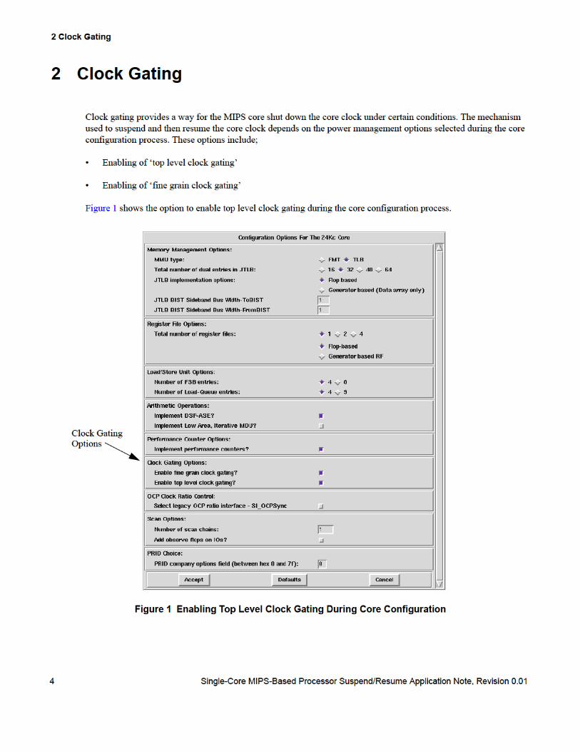

2 Clock Gating
Single-Core MIPS-Based Processor Suspend/Resume Application Note, Revision 0.01 5
2.1 Designs Implementing Top Level Clock Gating
Top level clock gating is provided as an option during the core configuration process. For designs implementing top level clock gating, there are two ways to place the MIPS core into sleep mode.
• Instruction-controlled power management
• Register-controlled power management
2.1.1 Instruction Controlled Clock Gating
Execution of the WAIT instruction can be used to place the MIPS core into sleep mode. When the WAIT instruction is executed during normal operation, the MIPS core completes all outstanding operations, then freezes the pipeline and asserts the SI_SLEEP signal, indicating to external logic that the MIPS core has entered sleep mode.
If top level clock gating is enabled, the processor turns off the internal clock to most of the MIPS core automatically once SI_SLEEP is asserted. The clock is maintained only for a small amount of logic that waits for an interrupt intended to bring the processor out of sleep mode. In addition to the interrupt logic, the following signals also remain active in sleep mode;
• SI_INT[5:0]
• SI_NMI
• SI_RESET
• EJ_DEBUGM
Once the clocks are suspended, the entire contents of the processor, including registers, caches, and TLB, are saved. Once the ‘wake’ interrupt is received, the processor restarts its internal clock and can resume normal operation within a few clock cycles. The ‘wake’ interrupt can be any enabled interrupt, NMI, or debug interrupt. This is the fastest and most efficient mechanism to transition the MIPS core in and out of sleep mode.
Note that the SI_RESET signal can also be used to exit sleep mode. However, assertion of SI_RESET causes all internal data to be lost and the registers to revert back to their default values.
2.1.2 Register Controlled Clock Gating
In addition to instruction controlled clock gating, the MIPS architecture allows for software to initiate entry into sleep mode via the register interface. The RP bit in the CP0 Status register can be set by software to indicate the desire to place the MIPS core into sleep mode. Once this bit is set, hardware asserts the SI_RP output signal.
On receipt of the SI_RP signal, external logic can then decide whether to suspend or reduce the frequency of the MIPS core accordingly. Note that this mechanism is different than instruction controlled clock gating in that the core does not determine whether the clock is suspended. Rather, external logic can decide to suspend the clock, reduce the
2 Clock Gating
6 Single-Core MIPS-Based Processor Suspend/Resume Application Note, Revision 0.01
clock frequency from its current level, or take no action.
2.1.3 Reduction of VDD During Sleep Mode
The information described above deals with clock gating only. In this example, during the time that the clocks are powered down, VDD remains at normal power levels. To obtain the maximum power savings during sleep mode, external logic can reduce the core VDD voltage once the MIPS core has asserted SI_SLEEP. This additional step can greatly reduce leakage and consequently power consumption during sleep mode. The minimum VDD voltage that can be used, and still allow the MIPS core to retain state, is process dependent.
The reduction of VDD can only be controlled by external means. The MIPS core does not provide a mechanism to reduce VDD internally during sleep mode. Note that if this option is implemented, it will take longer to restart the processor since the VDD must be ramped up to appropriate level before asserting the wake interrupt.
Refer to Section 3, "Power Gating" for more information.
2.1.4 Restart Latency Trade-Offs
Once the decision is made to enter sleep mode, some number of clocks are required to place the MIPS core into sleep mode, and bring the core out of sleep mode. In most designs, once sleep mode is entered, the core must remain in sleep mode for at least 100 clock cycles. Otherwise, the trade-off in time and power savings becomes negligible.
2.2 Designs Not Implementing Top Level Clock Gating
If top level clock gating was not enabled during the core configuration process, both instruction and register con-trolled power management can still be used. The main difference is the level of involvement of the MIPS core in either of these processes.
From an instruction standpoint, the WAIT instruction and SI_SLEEP signal can still be used to place the MIPS core into sleep mode. However, since top level clock gating is disabled, it is incumbent upon external logic to suspend the input clock to the processor. If the input clock is suspended, it is suspended to the entire MIPS core. As a result, the processor has no way to detect a ‘wake’ interrupt. Therefore, the assertion of SI_RESET is the only way to restart the MIPS core. Note that if this method is used, all data will be lost and the registers will revert back to their default val-ues.
From a register standpoint, software can still set the RP bit in the CP0 Status register to initiate the transfer to sleep mode. The processor responds by asserting the SI_RP bit to external logic. At this point, the MIPS core does not con-trol the clock behavior. It is incumbent upon external logic to provide the following functions:
• Suspend the core clock
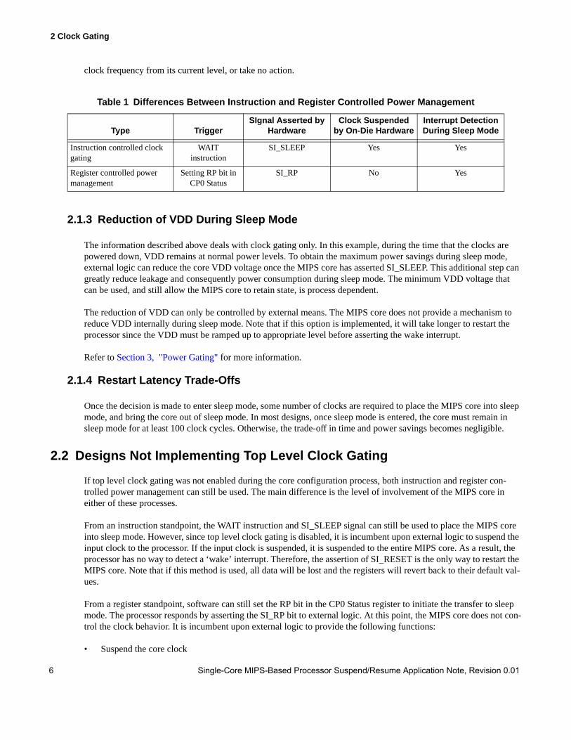
Table 1 Differences Between Instruction and Register Controlled Power Management
Type TriggerSIgnal Asserted by
HardwareClock Suspended
by On-Die HardwareInterrupt Detection During Sleep Mode
Instruction controlled clock gating
WAIT instruction
SI_SLEEP Yes Yes
Register controlled power management
Setting RP bit in CP0 Status
SI_RP No Yes

2 Clock Gating
Single-Core MIPS-Based Processor Suspend/Resume Application Note, Revision 0.01 7
• Reduce the core clock frequency
• Implement the interrupt detect function
2.3 Designs Implementing Fine Grain Clock Gating
Fine grain clock gating allows the MIPS core to shut down the clocks to individual blocks of logic within the chip as selected by the user. When the ‘fine grain clock gating’ option in Figure 1 is selected, separate clock domains are assigned to the various register blocks within the MIPS core. In the MIPS core, there is one write enable that is used to write all registers at once. If fine grain clock gating is enabled, the clock can be enabled only to the register block that is being accessed. The write enable for the other blocks is still driven, but no clock is supplied to those blocks not being accessed.
The implementation of fine grain clock gating requires the logic required to implement multiple clock trees within the MIPS core. Therefore, it works best in ASIC implementations where any number of clock domains can be assigned. It is less useful in FPGA implementations where the number of clock trees may be limited.
3 Power Gating
8 Single-Core MIPS-Based Processor Suspend/Resume Application Note, Revision 0.01
3 Power Gating
In addition to clock gating, power gating can be used to gain additional power savings. The saving and restoring of processor state can be used when the power savings provided by clock gating alone are not enough. In clock gating, the state of the processor need not be saved externally because even though the clocks are suspended, the power is still applied to the MIPS core, allowing the processor state to be saved internally.
In power gating, some or all of the power to the MIPS core can be shut down. This causes all data within the corre-sponding power domain(s) to be lost once the voltage falls below the retention value as defined by the process ven-dor. As a result, careful consideration must be taken to save some or all of the processor states before the power is shut down. Some of the logic blocks that can be saved prior to suspending the processor are:
• Registers (GPR, CP0, CP1, and/or CP2)
• Caches (instruction and/or data)
• Translation Lookaside Buffer (TLB)
• Scratch Pad RAM (Instruction and/or Data)
There are two methods that can be used to implement a suspend/resume mechanism in a MIPS core. These concepts are described in the following subsections.
• Hardware Suspend/Resume
• Software Suspend/Resume

3 Power Gating
Single-Core MIPS-Based Processor Suspend/Resume Application Note, Revision 0.01 9
3.1 Hardware Suspend/Resume
The hardware suspend/resume mechanism in the MIPS core allows the state of the caches, scratch pad RAM, and TLB to be transferred to memory via hardware using the suspend/resume (BIST) sideband signals that are defined during chip configuration. This process of moving data to and from the MIPS core is much faster than a pure software implementation.
The number of signals allocated to each group of BIST sideband signals are defined during configuration as shown in Figure 2.
\
Figure 2 Configuration of BIST Sideband Signals
Each group of BIST sideband signals shown in Figure 2 is described in Table 2 below.

3 Power Gating
10 Single-Core MIPS-Based Processor Suspend/Resume Application Note, Revision 0.01
The various BIST signals can be used to read and write external memory. For example, the BIST cache input signals can be used to read one or more of the cache lines. Hardware fetches and output the requested data onto the BIST cache output signals. Data on the output pins can then be transferred to a specific block of external memory.
In the MIPS architecture, all address space is memory mapped. To restore the data from memory, the boot vector side-band signals (SI_ExceptionBase[29:12]) can be programmed to point toward the block in memory where the proces-sor state was saved.
3.2 Software Suspend/Resume
For systems that have not implemented any hardware suspend/resume mechanism as described in the previous sec-tion, a software mechanism can be used to save state and power down the MIPS core. This section describes the tasks that should be performed during the suspend and resume processes.
3.2.1 Overview of Suspend/Resume Process
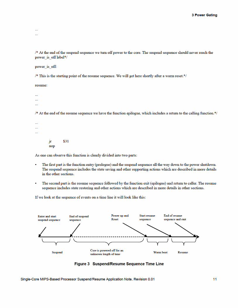
The recommended way of implementing a system suspend/resume in software is having a function that will perform a seamless suspend/resume operation. This means that to the rest of the software it looks like the function was entered and exited like any normal function, while in reality this function self-terminates in the middle of its execution by turning off the power the core, then resumes from where it left off shortly after power is restored.
At a high level, the assembly language skeleton should look like this:
/* Entry point to suspend/resume function, including the function prologue. */
suspend_resume:......
/* Here we start the suspend sequence */
suspend:...
Table 2 Definition of BIST Sideband Signals Used in Hardware Suspend/Resume
BIST Signal Name I/O Description
TPZ_MB_TOMBT_WIDTH I Cache sideband signals.
TPZ_MB_FROMMBT_WIDTH O Cache sideband signals.
TPZ_SP_EXT_TOSP_WIDTH I Data scratch pad signals.
TPZ_SP_EXT_FROMSP_WIDTH O Data scratch pad signals.
TPZ_ISP_EXT_TOISP_WIDTH I Instruction scratch pad signals.
TPZ_ISP_EXT_FROMISP_WIDTH O Instruction scratch pad signals.
TPZ_JTB_TOMBT_WIDTH I Joint TLB signals.
TPZ_JTB_FROMMBT_WIDTH O Joint TLB signals.

3 Power Gating
12 Single-Core MIPS-Based Processor Suspend/Resume Application Note, Revision 0.01
3.2.2 Suspend Process
During a software suspend process, the following tasks are recommended. Each of these tasks is described in the fol-lowing subsections.
• Save General Purpose Registers (GPR)
• Save some or all CP0 registers
• Flush the L1 data cache dirty lines and L2 cache dirty lines (if applicable)
• Save the return address
• Copy memory power down sequence into cache before switching memory to low-power mode (if applicable)
• Move memory to low-power mode (if applicable)
• Shut down power to the MIPS core
The GPR and CP0 registers are moved to the memory stack prior so that they can be easily retrieved when power is restored to the MIPS core. In this example, the registers would be moved to the stack and placed at the following memory offset addresses shown in Figure 4.

3 Power Gating
Single-Core MIPS-Based Processor Suspend/Resume Application Note, Revision 0.01 13
Figure 4 GPR and CP0 Register Locations in the Memory Stack
GPR1GPR2GPR3GPR4GPR5GPR6GPR7GPR16GPR17GPR18GPR19GPR20GPR21GPR22GPR23GPR26GPR27GPR28GPR29GPR30GPR31
Memory Stack
0x000x040x080x0C0x100x140x180x1C0x200x240x280x2C0x300x340x380x3C0x400x440x480x4C0x50
StatusConfig0Config1Config2Config3EbasePagemaskContext
0x540x580x5C0x600x640x680x6C0x70
Wired0x74
3 Power Gating
14 Single-Core MIPS-Based Processor Suspend/Resume Application Note, Revision 0.01
3.2.2.1 Save GPR Registers
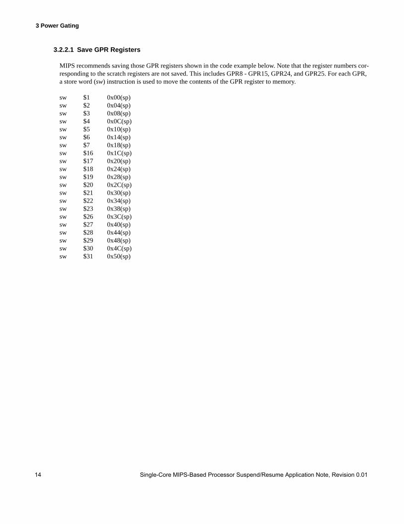
MIPS recommends saving those GPR registers shown in the code example below. Note that the register numbers cor-responding to the scratch registers are not saved. This includes GPR8 - GPR15, GPR24, and GPR25. For each GPR, a store word (sw) instruction is used to move the contents of the GPR register to memory.
sw $1 0x00(sp)sw $2 0x04(sp)sw $3 0x08(sp)sw $4 0x0C(sp)sw $5 0x10(sp)sw $6 0x14(sp)sw $7 0x18(sp)sw $16 0x1C(sp)sw $17 0x20(sp)sw $18 0x24(sp)sw $19 0x28(sp)sw $20 0x2C(sp)sw $21 0x30(sp)sw $22 0x34(sp)sw $23 0x38(sp)sw $26 0x3C(sp)sw $27 0x40(sp)sw $28 0x44(sp)sw $29 0x48(sp)sw $30 0x4C(sp)sw $31 0x50(sp)

3 Power Gating
Single-Core MIPS-Based Processor Suspend/Resume Application Note, Revision 0.01 15
3.2.2.2 Save CP0 Registers
In the MIPS architecture the CP0 registers cannot be moved directly to memory. Therefore, they must first be moved to a GPR register. In this example the registers are moved to the k0 scratch pad register, then from the k0 register to memory at the location shown in the corresponding sw instruction. Note that the offset addresses for each sw instruc-tion correspond to those shown in Figure 4.
As shown in the code snippet below, only a partial set of CP0 registers are saved. This is only an example. In some cases additional registers may need to be saved depending on the implementation.
mfco k0, CP0_STATUS /*Move from coprocessor 0, CP0_STATUS to k0*/sw k0, 0x54(sp) /*Store word k0 to offset 0x54 in memory*/mfco k0, CP0_CONFIG0 /*Move from coprocessor 0, CP0_CONFIG0 to k0*/sw k0, 0x58(sp) /*Store word k0 to offset 0x58 in memory*/mfco k0, CP0_CONFIG1 /*Move from coprocessor 0, CP0_CONFIG1 to k0*/sw k0, 0x5C(sp) /*Store word k0 to offset 0x5C in memory*/mfco k0, CP0_CONFIG2 /*Move from coprocessor 0, CP0_CONFIG2 to k0*/sw k0, 0x60(sp) /*Store word k0 to offset 0x60 in memory*/mfco k0, CP0_CONFIG3 /*Move from coprocessor 0, CP0_CONFIG3 to k0*/sw k0, 0x64(sp) /*Store word k0 to offset 0x64 in memory*/mfco k0, CP0_EBASE /*Move from coprocessor 0, CP0_EBASE to k0*/sw k0, 0x68(sp) /*Store word k0 to offset 0x68 in memory*/mfco k0, CP0_PAGEMASK /*Move from coprocessor 0, CP0_PAGEMASK to k0*/sw k0, 0x6C(sp) /*Store word k0 to offset 0x6C in memory*/mfco k0, CP0_CONTEXT /*Move from coprocessor 0, CP0_CONTEXT to k0*/sw k0, 0x70(sp) /*Store word k0 to offset 0x70 in memory*/mfco k0, CP0_WIRED /*Move from coprocessor 0, CP0_WIRED to k0*/sw k0, 0x74(sp) /*Store word k0 to offset 0x74 in memory*/
3.2.2.3 Flush Dirty Lines in L1 Data Cache
The following routine can be used to flush the dirty lines in a 32 Kbyte, 4-way set associative data cache with a 32-byte line size in preparation for shut-down. In this routine software examines each cache line and performs an invali-date on all non-dirty lines, and a writeback-invalidate on all dirty lines. A similar routine must be applied for L2 dirty lines in systems implementing a level 2 cache.
#define INDEX_BASE 0x80000000 // We use KSEG0 address as the base address for cache index access#define WAY_SIZE 0x2000 // size of one way in a 4-way set associative 32K cache (8K)#define WAYOFFSET 13 // offset of bits which determine the cache way to access#define ASSOC 4 // associativity (4 ways)#define LINE_SIZE 32 // size of each cache line#define IDX_WB_INV_DC 0x01 // code of index write-back invalidate D-cache operation
/* This macro performs the same cache op on 32 consecutive lines. */
#define cache32_unroll32(base,op) \
__asm__ __volatile__( \".set push \n" \".set noreorder \n" \".set mips3 \n" \"cache %1, 0x000(%0); cache %1, 0x020(%0)\n" \"cache %1, 0x040(%0); cache %1, 0x060(%0)\n" \

3 Power Gating
16 Single-Core MIPS-Based Processor Suspend/Resume Application Note, Revision 0.01
"cache %1, 0x080(%0); cache %1, 0x0a0(%0)\n" \"cache %1, 0x0c0(%0); cache %1, 0x0e0(%0)\n" \"cache %1, 0x100(%0); cache %1, 0x120(%0)\n" \"cache %1, 0x140(%0); cache %1, 0x160(%0)\n" \|"cache %1, 0x180(%0); cache %1, 0x1a0(%0)\n" \"cache %1, 0x1c0(%0); cache %1, 0x1e0(%0)\n" \"cache %1, 0x200(%0); cache %1, 0x220(%0)\n" \"cache %1, 0x240(%0); cache %1, 0x260(%0)\n" \"cache %1, 0x280(%0); cache %1, 0x2a0(%0)\n" \"cache %1, 0x2c0(%0); cache %1, 0x2e0(%0)\n" \"cache %1, 0x300(%0); cache %1, 0x320(%0)\n" \"cache %1, 0x340(%0); cache %1, 0x360(%0)\n" \"cache %1, 0x380(%0); cache %1, 0x3a0(%0)\n" \"cache %1, 0x3c0(%0); cache %1, 0x3e0(%0)\n" \
".set pop \n" \: \: "r" (base), \ "i" (op));
/* This function scans a 4-way set associative 32K bytes data cache with 32-byte line size and performs an index write-back invalidate cache operation on each of the cache lines.*/
static void flush_32k_4way_32byteline_dcache(void)
{ \unsigned long start = INDEX_BASE;unsigned long end = start + WAY_SIZE;unsigned long ws_inc = 1UL << WAYOFFSET;unsigned long ws_end = ASSOC << WAYOFFSET;unsigned long ws, addr;
/* For every way (ws = the bits in the address which dertmine the cache way to access). */for (ws = 0; ws < ws_end; ws += ws_inc)
/* In each way go from start to end address. */for (addr = start; addr < end; addr += LINE_SIZE * 32)
/* Each time we perform the cache op on 32 lines. The address is a combination of the cache line offset in side the way (addr) and the way bits (ws).*/cache32_unroll32(addr|ws, IDX_WB_INV_DC);

3 Power Gating
Single-Core MIPS-Based Processor Suspend/Resume Application Note, Revision 0.01 17
3.2.2.4 Save the Resume Address
This routine takes the starting address of the resume sequence and saves it somewhere on the board, external to the MIPS core. Later, after power up and reset, the warm boot sequence retrieves that address and jumps to it. This ini-tiates execution of the resume process.
3.2.2.5 Copy Memory Power Down Sequence Into Cache
This piece of code loads the remaining instructions of the suspend sequence into the instruction cache. This is done since the memory (e.g. DRAM) is about to be put in low power mode and thus become inaccessible to the core. It is important that all instruction fetches hit in the instruction cache because if they miss the core won't be able to fetch them from memory.
*/
.set noreorder
/* load the start address and end address of the remaining instructions */
la $8, mem_to_low_powerla $9, post_suspend /*after power is removed*/
/* Now fill the cache line by line starting from the start address and incrementing the address by a line size in each iteration until we get beyond the en address.*/
fill_icache:
cache 0x14, 0($8)addiu $8, $8, 32bltu $8, $9, fill_icachenop
mem_to_low_power:
3.2.2.6 Move Memory to Low Power Mode
/* Here we have a sequence of instructions that will move the memory to low power mode. These instructions used to perform this function are SOC specific depending on the particular way the memory is implemented and addressed.*/
...
...
...
/* The following label comes after the end of the suspend sequence. We should never get here because we are sup-posed to loose power earlier.*/
post_suspend:
3.2.2.7 Shut Down Power to the MIPS Core
Once all of the above tasks have been performed, power to the MIPS core can be suspended by reducing VDD to 0V. This task is performed by the SOC and is implementation-dependent.

3 Power Gating
18 Single-Core MIPS-Based Processor Suspend/Resume Application Note, Revision 0.01
3.2.3 Resume Process
During the software resume process, the following tasks are recommended. The tasks are handled in the opposite order in which they were executed during the suspend operation.
• System Wake-up
• Power-Up VDD to the MIPS Core and Assert Power-On Reset
• Warm/Cold Boot Detection
• Exit memory low-power mode
• Initialize caches and TLB
• Jump to resume address
• Restore CP0 registers
• Restore GPR registers
3.2.3.1 System Wake-Up
In a typical system the power management (PM) module stays active after the system enters suspend mode. This component will consume very little power but will keep monitoring external signals that may trigger the system to resume normal operation. Once a trigger is detected, the PM block will wake up various system components, one of these being the MIPS core. Since power to the core was shut down earlier, the core must be powered up and brought to its Reset state.
3.2.3.2 Power-Up VDD to the MIPS Core and Assert Power-On Reset
Once the system logic detects a resume condition, the system power management block must raise the VDD levels of the MIPS core to there normal operating levels and allow the voltage to stabilize. Once the voltages are stabilized, assert the power-on reset pin to the MIPS core.
3.2.3.3 Warm/Cold Boot Detection
When a processor core goes to its reset state it starts executing instructions from its Reset vector address. We call the initial sequence of instructions "boot" and it typically starts executing off of "boot ROM" memory. At this point the system must distinguish between two boot modes: cold boot and warm boot.
• A cold boot is typically performed when the entire system is powered up and has to initialize all of its hardware components. In this scenario there is typically no (or little) memory of the system's state prior to boot (although some systems will save configuration information in non-volatile memory). After the initial boot the operating system has to go through its own complete boot sequence which takes a relatively long time.
• A warm boot is typically performed to resume a system that was previously suspended for power saving. In this case much of the system state prior to boot is available and can be restored (for example, it was saved into a memory component which did not loose power or otherwise in non-volatile memory). The warm boot sequence is typically short as users expect instant response (from a user point of view the system is available even when it was suspended for power saving). A warm boot does not require the operating system to perform its full boot sequence. For the most part the OS will continue from where it left off.
3 Power Gating
Single-Core MIPS-Based Processor Suspend/Resume Application Note, Revision 0.01 19
In the case of a warm boot, the boot software sequence starts from the same place (the Reset vector address) whether it is a cold boot or warm boot condition. However, shortly thereafter it detect its mode whether it is a cold or warm boot. If the system resumes from suspend mode, the boot software will detect this and decide to perform a warm boot. The indication that the system is coming back from suspend mode may be available in the PM block or in some piece of memory. This mechanism is implementation dependent.
Once a decision is made to perform a warm boot and not a cold boot, the warm boot sequence will perform a basic initialization and then jump to the resume address in the suspend/resume function. The resume address will be avail-able in an implementation dependent location where it was saved by the suspend sequence. Then, as discussed earlier, the function will restore some system state and return to its caller as if nothing ever happened. The caller may have no indication that the system was suspended for a while.
Examples of basic core initialization that must be carried out regardless of the boot mode are caches and TLB initial-ization. Many users will opt not to save and restore their cache and/or TLB states. Note that the MIPS core caches and TLB wake-up in a random state and must be initialized before data can be written to them.
3.2.3.4 Exit Memory Low-Power Mode
This is an optional system-dependent function. If the external memory devices were placed in low-power mode dur-ing the suspend process, the memory must exit its low-power mode before the instructions stored to the stack during the suspend process can be fetched by the MIPS core.
3.2.3.5 Initialize Caches and TLB
The initialize caches and TLB routines are always performed when reset is asserted to the MIPS core. This is done to bring the caches to an initial state. This routine would be exactly the same as the one used in the boot example that accompanies the delivery of each MIPS core. Refer to the boot example associated with the MIPS core package.
3.2.3.6 Jump to Resume Address
At this point the boot process is done with general initialization process initiated by the assertion of reset and is ready to start the actual resume sequence. It retrieves the starting address of the resume sequence that was saved earlier (as part of the suspend sequence) and jumps to it, thereby initiating execution of the resume sequence.

3 Power Gating
20 Single-Core MIPS-Based Processor Suspend/Resume Application Note, Revision 0.01
3.2.3.7 Restore CP0 Registers
In the MIPS architecture the CP0 registers cannot be moved directly from memory. Therefore, they must first be moved to a GPR register. In this example the registers are moved to the k0 scratch pad register, then from the k0 reg-ister to memory at the location shown in the corresponding lw instruction. Note that the offset addresses for each lw instruction correspond to those shown in Figure 4.
lw k0, 0x74(sp) /*Load word k0 from offset 0x74 in memory*/mtco k0, CP0_WIRED /*Move to coprocessor 0, CP0_WIRED from k0*/lw k0, 0x70(sp) /*Load word k0 from offset 0x70 in memory*/mtco k0, CP0_CONTEXT /*Move to coprocessor 0, CP0_CONTEXT from k0*/lw k0, 0x6C(sp) /*Load word k0 from offset 0x6C in memory*/mtco k0, CP0_PAGEMASK /*Move to coprocessor 0, CP0_PAGEMASK from k0*/lw k0, 0x68(sp) /*Load word k0 from offset 0x68 in memory*/mtco k0, CP0_EBASE /*Move to coprocessor 0, CP0_EBASE from k0*/lw k0, 0x64(sp) /*Load word k0 from offset 0x64 in memory*/mfco k0, CP0_CONFIG3 /*Move to coprocessor 0, CP0_CONFIG3 from k0*/lw k0, 0x60(sp) /*Load word k0 from offset 0x60 in memory*/mtco k0, CP0_CONFIG2 /*Move to coprocessor 0, CP0_CONFIG2 from k0*/lw k0, 0x5C(sp) /*Load word k0 from offset 0x5C in memory*/mtco k0, CP0_CONFIG1 /*Move to coprocessor 0, CP0_CONFIG1 from k0*/lw k0, 0x58(sp) /*Load word k0 from offset 0x58 in memory*/mtco k0, CP0_CONFIG0 /*Move to coprocessor 0, CP0_CONFIG0 from k0*/lw k0, 0x54(sp) /*Load word k0 from offset 0x54 in memory*/mtco k0, CP0_STATUS /*Move to coprocessor 0, CP0_STATUS from k0*/

3 Power Gating
Single-Core MIPS-Based Processor Suspend/Resume Application Note, Revision 0.01 21
3.2.3.8 Restore GPR Registers
MIPS recommends loading those GPR registers shown in the code example below. Note that the register numbers corresponding to the scratch pad registers are not loaded. This includes GPR8 - GPR15, GPR24, and GPR25. For each GPR, a load word (lw) instruction is used to move the contents of the corresponding memory location into the GPR.
lw $31 0x50(sp)|lw $30 0x4C(sp)lw $29 0x48(sp)lw $28 0x44(sp)lw $27 0x40(sp)lw $26 0x3C(sp)lw $23 0x38(sp)lw $22 0x34(sp)lw $21 0x30(sp)lw $20 0x2C(sp)lw $19 0x28(sp)lw $18 0x24(sp)lw $17 0x20(sp)lw $16 0x1C(sp)lw $7 0x18(sp)lw $6 0x14(sp)lw $5 0x10(sp)lw $4 0x0C(sp)lw $3 0x08(sp)lw $2 0x04(sp)lw $1 0x00(sp)
4 Additional Power Management Options
22 Single-Core MIPS-Based Processor Suspend/Resume Application Note, Revision 0.01
4 Additional Power Management Options
The following power management options can be implemented by the SOC vendor to further reduce system power. Note that these ideas and are outside the scope of this document.
4.1 Dynamic Scaling
Dynamic scaling is the process of changing the CPU operating voltage and/or clock frequency in real time. This is a complex process where software controls the operating voltage and clock generator and anticipates the workload. When high CPU workload is anticipated the software adjusts the clock frequency up to permit faster execution. When the high workload is completed, the clock is adjusted back down to a lower frequency to reduce power.
Dynamic scaling requires real time control of the core voltage regulator and clock phase lock loop. Dynamic scaling is complicated to implement but can yield significant power reduction in systems where the CPU is the dominant power consumer and large variations in workloads are common. Examples of these types of systems are network pro-cessors, disk array controllers and servers.
4.2 Targeted Semiconductor Process
The semiconductor process should be selected that matches with the SOC application. Finer geometries will yield faster chips but at a cost of higher leakage power. Your foundry is the best resource for further information on process selection.
4.3 Leakage Control
Leakage is a major contributor to power consumption in fine geometry processes. There are active and passive meth-ods for reducing leakage. Consult with your foundry for advice.

5 Document Revision History
Single-Core MIPS-Based Processor Suspend/Resume Application Note, Revision 0.01 23
5 Document Revision History
Change bars (vertical lines) in the margin of this document indicate significant changes in this document since its last release. Change bars are removed for changes that are more than one revision old.
Revision Date Description
0.01 June 23, 2010 First release, beta version

Unpublished rights (if any) reserved under the copyright laws of the United States of America and other countries. This document contains information that is proprietary to MIPS Tech, LLC, a Wave Computing company (“MIPS”) and MIPS’ affiliates as applicable. Any copying, reproducing, modifying or use of this information (in whole or in part) that is not expressly permitted in writing by MIPS or MIPS’ affiliates as applicable or an authorized third party is strictly prohibited. At a minimum, this information is protected under unfair competition and copyright laws. Violations thereof may result in criminal penalties and fines. Any document provided in source format (i.e., in a modifiable form such as in FrameMaker or Microsoft Word format) is subject to use and distribution restrictions that are independent of and supplemental to any and all confidentiality restrictions. UNDER NO CIRCUMSTANCES MAY A DOCUMENT PROVIDED IN SOURCE FORMAT BE DISTRIBUTED TO A THIRD PARTY IN SOURCE FORMAT WITHOUT THE EXPRESS WRITTEN PERMISSION OF MIPS (AND MIPS’ AFFILIATES AS APPLICABLE) reserve the right to change the information contained in this document to improve function, design or otherwise. MIPS and MIPS’ affiliates do not assume any liability arising out of the application or use of this information, or of any error or omission in such information. Any warranties, whether express, statutory, implied or otherwise, including but not limited to the implied warranties of merchantability or fitness for a particular purpose, are excluded. Except as expressly provided in any written license agreement from MIPS or an authorized third party, the furnishing of this document does not give recipient any license to any intellectual property rights, including any patent rights, that cover the information in this document. The information contained in this document shall not be exported, reexported, transferred, or released, directly or indirectly, in violation of the law of any country or international law, regulation, treaty, Executive Order, statute, amendments or supplements thereto. Should a conflict arise regarding the export, reexport, transfer, or release of the information contained in this document, the laws of the United States of America shall be the governing law. The information contained in this document constitutes one or more of the following: commercial computer software, commercial computer software documentation or other commercial items. If the user of this information, or any related documentation of any kind, including related technical data or manuals, is an agency, department, or other entity of the United States government ("Government"), the use, duplication, reproduction, release, modification, disclosure, or transfer of this information, or any related documentation of any kind, is restricted in accordance with Federal Acquisition Regulation 12.212 for civilian agencies and Defense Federal Acquisition Regulation Supplement 227.7202 for military agencies. The use of this information by the Government is further restricted in accordance with the terms of the license agreement(s) and/or applicable contract terms and conditions covering this information from MIPS Technologies or an authorized third party. MIPS, MIPS I, MIPS II, MIPS III, MIPS IV, MIPS V, MIPSr3, MIPS32, MIPS64, microMIPS32, microMIPS64, MIPS-3D, MIPS16, MIPS16e, MIPS-Based, MIPSsim, MIPSpro, MIPS-VERIFIED, Aptiv logo, microAptiv logo, interAptiv logo, microMIPS logo, MIPS Technologies logo, MIPS-VERIFIED logo, proAptiv logo, 4K, 4Kc, 4Km, 4Kp, 4KE, 4KEc, 4KEm, 4KEp, 4KS, 4KSc, 4KSd, M4K, M14K, 5K, 5Kc, 5Kf, 24K, 24Kc, 24Kf, 24KE, 24KEc, 24KEf, 34K, 34Kc, 34Kf, 74K, 74Kc, 74Kf, 1004K, 1004Kc, 1004Kf, 1074K, 1074Kc, 1074Kf, R3000, R4000, R5000, Aptiv, ASMACRO, Atlas, "At the core of the user experience.", BusBridge, Bus Navigator, CLAM, CorExtend, CoreFPGA, CoreLV, EC, FPGA View, FS2, FS2 FIRST SILICON SOLUTIONS logo, FS2 NAVIGATOR, HyperDebug, HyperJTAG, IASim, iFlowtrace, interAptiv, JALGO, Logic Navigator, Malta, MDMX, MED, MGB, microAptiv, microMIPS, Navigator, OCI, PDtrace, the Pipeline, proAptiv, Pro Series, SEAD-3, SmartMIPS, SOC-it, and YAMON are trademarks or registered trademarks of MIPS and MIPS’ affiliates as applicable in the United States and other countries. All other trademarks referred to herein are the property of their respective owners. {ƛƴƎƭŜπ/ƻNJŜ aLt{π.ŀǎŜŘ tNJƻŎŜǎǎƻNJ {dzǎLJŜƴŘκwŜǎdzƳŜ !LJLJƭƛŎŀǘƛƻƴ bƻǘŜΣ wŜǾƛǎƛƻƴΥ лΦлм
Copyright © Wave Computing, Inc. All rights reserved. www.wavecomp.ai