Embed Size (px)
Citation preview
Sustratos
Curso 15-16
Prof. Andrés Roldán Aranda
4º Curso Grado en Ingeniería de
Tecnologías de Telecomunicación

Contenidos
1.- Introducción 2.- Proceso de Fabricación de Placas 3.- Sustratos y tecnologías 4.- Surface Mount Technology 5.- Stencils 6.- Dimensionado de pistas

Fase 1: Front-end tool data preparation

Fase 2: Preparing the phototools

Fase 3: Print inner layers
1. 2.
3. 4.

Fase 4: Etch inner layers

Fase 5:
Register punch and Automatic Optical Inspection (AOI)

Fase 6: Lay-up and bond

Fase 7: Drilling the PCB

Fase 8: Electroless copper deposition

Fase 9: Image the outer layers
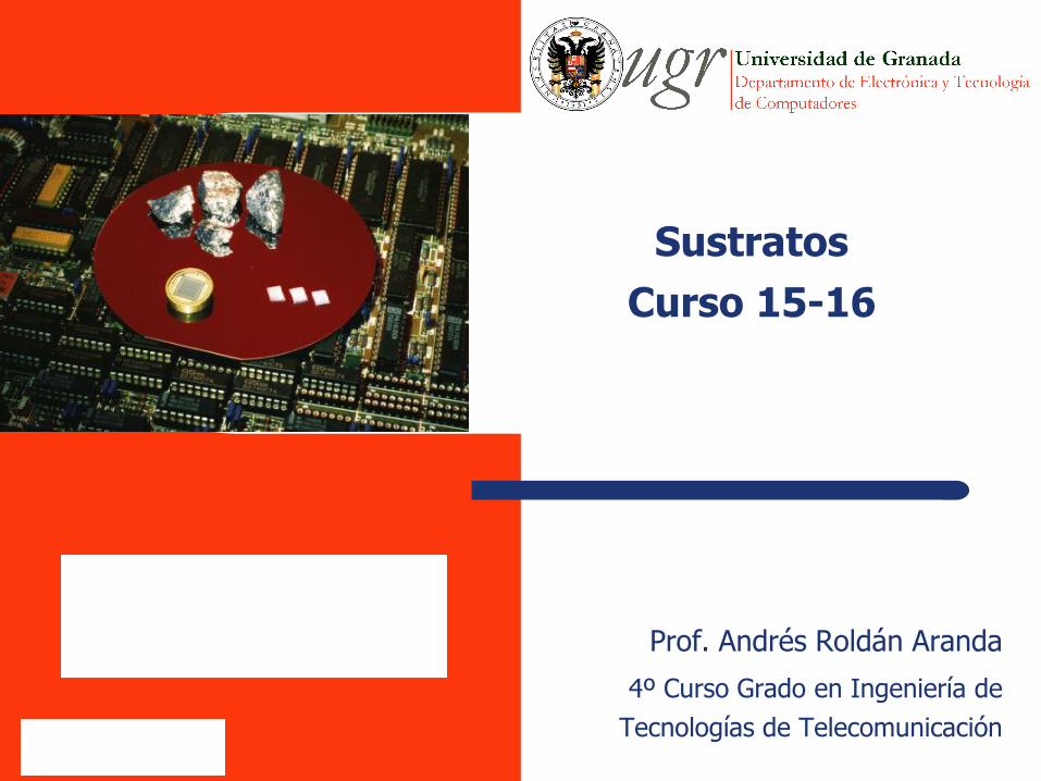
Fase 10: Electroplate the boards with copper

Fase 11: Etch outer layers

Fase 12: Apply soldermask

Fase 13:
RoHS-compliant surface finishes – electroless
gold over nickel
RoHS : Reduction of Hazardous Substances
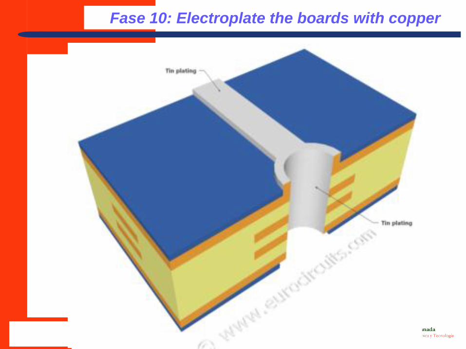
Fase 14: Plated Hard-gold edge connectors
electro-plate 1 – 1.5 microns of gold over 4 – 5 microns of plated nickel

Fase 15: Silk-screen and cure
Ink-jet image printing needs no set-up Ink-jet image printing needs no set-up.
10 minutes using a 5 stage conveyorised oven

Fase 16: Electrical test
Using a flying probe tester we check each net to ensure that it is
complete (no open circuits) and does not short to any other net
Test speed 25,4 mm/s
With 4096 test pins
The scan consists of
thousands of 0.1mm
diameter probes, gentle
as a human hair,
brushing over the PCB,
producing an electrical
picture as they scan.

Fase 17: Profiling. V-Cut scoring

Fase 18:
Final inspection - vacuum-sealed to keep out dirt
and moisture

Substrate Technologies

LGA Module Construction

Substrate Construction

2D Module Integration Technologies

Surface Mount Technology
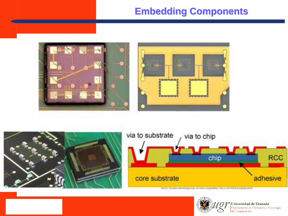
Embedding Components

Wafer level integration

3D Model Integration

Via Types

Via Pitch and Wiring Channel

Solder Mask Defined Pads

Linear Technology Corporation
Mixed Pads (SMD and NSMD)

Thermal Relief: NSMD

PCB Plane Separation
Maximum solder mask opening for plane separation needs to be controlled; Stencil opening in this area can be reduced to 0.6 to ensure no bridging; Critical area – under Inductor and plane separation

Laser solder paste stencil

Mylar solder paste stencil
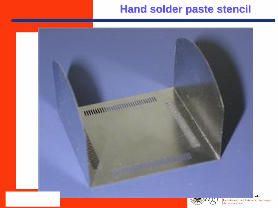
Hand solder paste stencil

Signal Integrity

Routing

Determination of Component Arrangements

Force Directed Placing

Substrate Technologies – Laminates
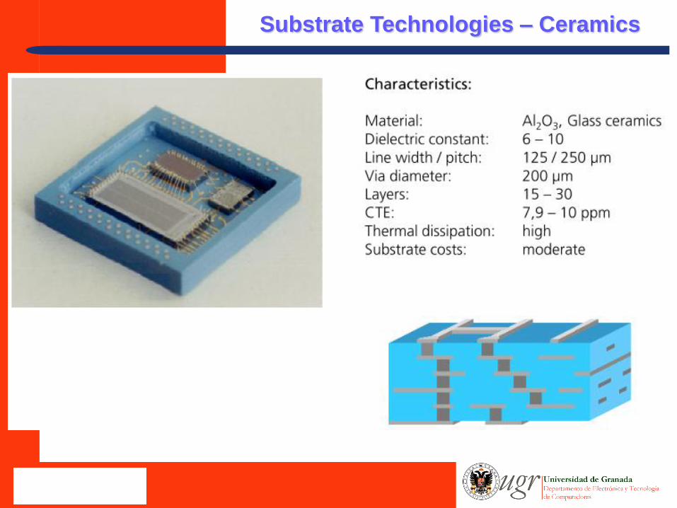
Substrate Technologies – Ceramics

Substrate Technologies – Thin Film

Area versus Packaging Types

Miniaturization by
Novel Assembly Technologies / Directassembly

Miniaturization by
Novel Assembly Technologies / Directassembly
Flip Chip Wirebonding

Footprint – Wire Bonding versus Flip Chip

Footprint of Flip Chip – Contact

Footprint of Wire Bonding – Contact

High Packing Density by 3-D Packaging

Roundup of the Technology – Parameters

Wire Bounding Example
Gold wire bonding - Video-1
Wire bonding - Video-2

High Packing Density by 3-D Packaging

Example for the layout of a wiring bearer
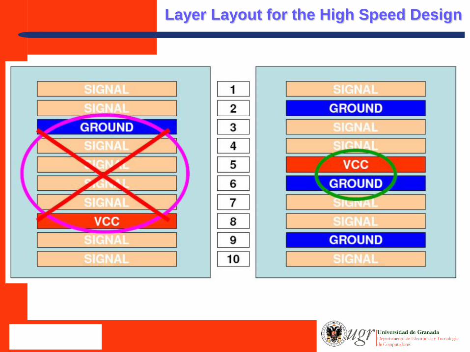
Layer Layout for the High Speed Design

Signal Integrity

Determination of Process Costs

Description of Macro-Processes (e.g. Pick & Place)

Determination of Substrate Costs

Assembly Technologies
MCM: Multi Chip Module (MCM) is an electronic system or subsystem with two or more bare integrated circuits (bare die) or Chip Sized Packages (CSP) assembled on a substrate

Assembly Technologies
VCM: Voice Coil Motor. The incumbent actuator technology for miniature AF cameras is the voice coil motor. VCMs are named as such because they are based on the principles of attraction and repulsion between magnets to generate sound from electricity. The technology was first patented in 1874
VCM : is the incumbent technology used ina miniature camera to move a lens module and alter focus. The technology, shown in an 1888 patent by Alex. Graham Bell (left), is not fundamentally different from the VCM in a HTC OneX+ smartphone (right)

Determination of Assembly Costs

Uso de dos monitores Vista
Moderador
http://office.microsoft.com/es-
es/powerpoint-help/dar-una-
presentacion-en-dos-monitores-
mediante-la-vista-moderador-
HA010067383.aspx?CTT=5&origi
n=HP010374495

Control de la energía

The copper in a PCB is rated in ounces, and represents the
thickness of 1 ounce of copper rolled out to an area of 1 square
foot.
For example a PCB that uses 1 oz. copper has a thickness of
1.4mils.
Track thickness
Ounces Thickness (mil) Thickness (um)
1/2 oz. 0.7 mil 17.6
1 oz. 1.4 mil 35
2 oz. 2.8 mil 70
Ounces Min Cu (mil) Thickness (mil) plated
1 oz. 1.22 mil 2.08 mil (53.248 um)
2 oz. 2.43 mil 3.30 mil (84.48 um)
3 oz. 3.65 mil 4.51 mil (115.456 um)
4 oz. 4.86 mil 5.69 mil (145.664 um)
IPC-2221A “Generic Standards on Printed Circuit Board Design”

• Calentamiento de las pistas
• La máxima corriente que admite una pista está limitada por el
autocalentamiento
• Hay que considerar la presencia de elementos calientes cercanos
• Mantener t < 120ºC para FR4
• Regla: - w > 0.3 mm/A, para 1 oz (t < 30ºC e
- w > 0.18 mm/A, para 2 oz I < 5 A)
• El “plating” o metalizado puede aumentar el espesor de las pistas
en un 40%
• El estañado de las pistas prácticamente no ayuda
thrms RPtRIP ·,2
Calentamiento de las pistas

• Calentamiento de las pistas: Resistencia
- Efecto pelicular:
L
w t tw
LR
··
)35(·5.010·5.5: 117 mtparaw
LmRmCu
2··.
2
w
LRt
mMHzf
mMHzf
mMHzf
142100
42210
13621
Calentamiento de las pistas

0.44 0.725I k T A
(Temperature Rise)
0.048 for outer layers
0.024 for inner layer
Trace cross - sectional area
MAX AMBIENTT T T
k
A
Current Carrying Capability*
* IPC-2221A “Generic Standards on Printed Circuit Board Design”

Current Carrying Capability*
* IPC-2221A “Generic Standards on Printed Circuit Board Design”

Current Carrying Capability*
* IPC-2221A “Generic Standards on Printed Circuit Board Design”

• Calentamiento de las pistas
• Un valor práctico: Rth =
30ºC/W (cápsula a ambiente)
• Rth mejora con el área,
hasta 1” para 1 oz, y unas
3” para 2 oz
• FR4 es buen conductor
térmico un plano de Cu
en el otro lado ayuda en un
10-20% (hasta un 50-70%
con vías térmicas)
Calentamiento de las pistas

Calentamiento de las pistas
Norma IPC-2152:
“Standard for Determining
Current-Carrying Capacity
In Printed Board Design”

Calentamiento de las pistas

Calentamiento de las pistas

Calentamiento de las pistas

Calentamiento de las pistas

Disipación térmica

Disipación térmica


Thermal Pads

Via Stiching:
PROCEDIMIENTO
http://wiki.altium.com/di
splay/ADOH/Via+Stitchi
ng

Pads for Density Levels

Electrical Clearance
IPC 2221A: AC and pulsed voltages > 200V must consider
dielectric and capacitive effects of substrate in addition to
spacing.
Withstand Voltage Min. Spacing
0-30 V 3.9 mil
31-150 24.0 mil
151-300 49.2 mil
301-500 98.4 mil

IPC –2221A: “Generic Standard on PCB Design”
UL 8402: “Insulation Coordination Including Clearance and
CreepageDistances for Electrical Equipment”
ANSI/ISA S82.01: “Safety Standard for Electrical and
Electronic Test, Measuring, Controlling, and Related
Equipment –General Requirements”
IEC 61010-1: “Safety Standard for Electrical and Electronic
Test, Measuring, Controlling, and Related Equipment –Part
1: General Requirements”
UL 746E: “Standard Polymeric Material used in Printed
Wiring Boards”
Web Site: http://www.energy.ece.uiuc.edu/balog
Selected References