Embed Size (px)
Citation preview

NASA Contractor Report 194922
Y" i J "Z "/
Switched-Beam Radiometer Front-End
Network Analysis
IL J. Trew
Case Western Reserve University, Cleveland, Ohio
G. L. Bilbro
North Carolina State University, Raleigh, North Carolina
(NASA-CR-194922) SWITCHED-BEAM
RADIOMETER FRONT-END NETWORK
ANALYSIS Final Report (North
Carolina State Univ.) 32 p
N94-35247
Unclas
Grant NAG1-943
June 1994
G3/32 0012659
National Aeronautics and
Space Administration
Langley Research CenterHampton, Virginia 23681-0001
https://ntrs.nasa.gov/search.jsp?R=19940030741 2018-09-08T13:12:29+00:00Z


Table of Contents
If.
Ill.
IV.
Introduction
Delay Line Investigation
Delay Line Implementation
Antenna Element Model
Simulation Results
Delay Line Architecture
Noise Figure and Combiner Loss
Monte Carlo Tolerance Simulation
Phase Shifters
Conclusions
Pa_a
1
3
3
4
7
8
13
13
17
27
Addendum 28


I. Introduction
Switched-beam networks offer the potential to fabricate
electronically steered antennas with RF performance characteristics
superior to mechanically steered configurations. This concept has been
widely developed and employed for phased-array radars, but has not
been thoroughly investigated for radiometer applications. The radiometer
application is, in many regards, much more difficult for switched-beam
networks than encountered in phased-array radars for a basic reason. In
a radar a coherent signal is transmitted to a target and the return signal
compared to the original to determine certain parameters of interest
about the target, such as range, velocity, etc. The active signal is the
main information carrier and since it's characteristics such as frequency,
phase, and amplitude are known, it is only necessary to determine how
the transmission path and target modify the signal to extract the
information of interest. Noise acts to contaminate the signal, but
primarily serves to place a limit upon the useful operating range of the
radar. Radiometers, conversely, operate on a fundamentally different
principle. They do not transmit a source signal, but measure the natural
radiation emissions from the target scene. As such, they measure
whatever radiation emissions are present within the antenna beamwidth.
Noise generated within the path between the target scene and radiometer
or within the antenna/network circuit will contaminate the desired
radiometer signal. Since the instrument is basically measuring noise, it
is, in general very difficult to differentiate between the path/system noise
and the desired target emissions.
The noise contamination problem can be minimized by proper
calibration procedures. In this manner it is possible to measure or
calculate the characteristics of the noise generation mechanisms between
the target scene and the instrument read-out. Once the noise
characteristics are known, they can be subtracted from the composite
signal to yield the desired target scene. As long as the unwanted signals
are deterministic it is possible to improve the instrument performance by
calibration. Unfortunately, certain signals are not deterministic and
cannot be removed from the composite signal by calibration. These
signals can prove very troubling and will present limitations to system
sensitivity. Examples of this type of signal include anything that has a
basically random performance characteristic. For example, a switch thatalternates between two positions is deterministic only if it returns to
exactly the same position every time it is activated. Since a physicalswitch will have tolerances associated with its operation, it will not have
exactly the same characteristics every time it switches. The tolerances
depend upon both mechanical and electrical parameters. The tolerance
problem ultimately will define the sensitivity of a radiometer, since smallvariations in the device impedance will produce slight impedance
discontinuitie_ that will generate noise. The noise generated from the
performance tolerances is not deterministic and cannot be calibrated outand will, therefore, place a limitation upon the radiometer sensitivity.
The problem is fundamental to the use of switched-beam networks
for radiometers. The purpose of this study is to investigate this issue.
Specifically, a particular combiner network is modeled and investigatedin order to determine its noise performance. The network consists of a
series of parallel delay lines with an ideal antenna element at one endand connected together by means of an ideal combiner. The noise
performance of a lossy combiner and the use of such an element inswitched-beam radiometer front-ends is also considered and reported.
The effects of delay line fabrication were also considered and preliminary
work directed towards investigation of the noise performance of example
phase shift elements is reported.

11. Delay Line Investigation
For this investigation a series of delay lines fabricated from
microstrip were simulated using the Hewlett-Packard Microwave Design
System. The lines were operated for a band of frequencies centered at fo -
4.3 GHz. The wavelength in free space corresponding to this frequency is
k = 2.75 inches or k = 0.229 feet. Arrays with 2 < N > 16 elements placed
on k/2 centers were simulated. The investigation considers one
dimensional angular sweeps. The angle was allowed to vary from on-axis
boresight (zero degrees) to +/- 45 °. Since the array is symmetric, it is
sufficient to consider only positive angles as the negative angles will be
simple mirror images of the positive angle results. The angle is measured
in terms of the free space distance between adjacent elements. This
length is extended out to k/2, which corresponds to an "end-fire"
orientation of 90 ° . The results are presented so that the center of the
plots corresponds to the 45 ° angular location. Narrow bandwidths of a
few percent are considered so that dispersion has negligible effects upon
the performance of the array. Although most of the work considered the
use of microstrip transmission lines, other transmission media, including
TEM transmission lines, were considered. The TEM transmission lines,
however, are considered impractical for lengths of a few inches that are of
interest for the frequency and array size investigated in this work.
Delay Line Implementation
The microstrip model used in the simulation is selected so that the
signal is attenuated at a rate of 2.5 db/foot, which is significantly lossier
than obtained with coaxial transmission lines. This is not restrictive,
however, since the simulations predict that for small arrays the
attenuation is negligible compared to other effects in the system. High
attenuation rates result in the noise figure being dependent upon the
steering angle, but this effect is not significant for losses up to about 5
db/foot. The delay lines are assumed to be switched by PIN diodes which
introduce negligible noise compared to other effects in the system.
An alternative to delay lines are electrically controlled filters with
specifically designed phase characteristics. In this type of network the
delay is established primarily by varactor diodes, which can be tuned bybias to present the correct impedance to generate the desired delay. This
operation is in contrast to the use of the varactor diodes as switches
where they simply switch lengths of transmission line in or out of thenetwork. The varactor diodes in the filter network will have reactance
characteristics that are strongly determined by the electronic bias andthe reactance tolerance will be directly dependent upon the .bias
tolerance of the source. Unless extremely stable bias sources are
employed this type of network may contribute significant noise. Theamount of noise will be a function of the diode resistance as well as the
bias source stability. This type of network has the advantage of small sizeand easy integration, however, and may be useful for the switched beam
application. Due to time limitations it was not possible to completely
investigate these networks at this time, but they should be investigatedin more detail due to the potential advantages offered.
Antenna Element Model
Several circuits were evaluated for the switched-beam radiometer
front-end network. Two general models were investigated in detail. Both
network models use arrays of delay lines with realistic loss and both use
power combiners to combine the output from the delay lines into a 50
load. The two models differed in the details of the method used to
simulate the antenna and free space propagation. One model used power
splitters to distribute the output of a source to lossless delay lines used
to model free space propagation. That model was found to not accurately
model the desired network for reasons that will be discussed. A model
that accurately simulated the desired network was constructed by use of
voltage-controlled voltage sources with specified phase. These elements
permitted the free space wave to be simulated for any incident angle by
control over the individual phase at each source. The resulting circuit for
a 4 element network is shown in Fig. 1 and was used for this
investigation.

Ollm
PCRTi N-_-_I i._
T_,O i" " _ I $[_.z)-n $-.z)-_
T I t[_)-O z_z.)-_" =1 i .rc_, *U.-_
D m m
P(_TI _-__m.m.mm
"' _ I |th.';_' tt;:;;-'_ t-T" t ++++,..,o+ +r+z++.,_ I
- -I j. _.._ au.,.o I_ + ,5,
""" %,.-,,/ I s[:.zJ-r3 SCZ,2],qTT I zt_)-_ zt+++].._
- -I J. Ec,-_:. +u.,.a
,9--- ,_,_ C'_tk_r L_ LU..I
CCt_T tmm LLII_O. 5eC,_
Cm_T[_N PTol. II
ZISI31T.LI0_ .] I olL0SS TS0LATI_,I. IZ I dl
_JIE_IT- +-]'l't'1 0_ 1')4t_:]lT.l.0_.| I - 11.1:_
IM_MT LOSS Z1 _l.O_
_ATIm_i. R t a
p|
"" .;. _ Iz_/ I l
" _ ..... I--"I" "F " + o_,.,, ( "_ I -,._...o i " _o, _I "rI,,.,''--• _ I S|l.t)_'4 S_.Z)-_l
T I zt,].m z_[r)-m I _-o:o_ I I r-'-"- -! i _-,_, _,,m j
RGIOUNO I_,ROUKO£OLt_TIl:14 M.Mo.i| [gl.V, TTOI4 U.A'I.IP_UIIIllJ_L
+
mm-Jm_ _-o:o ox
r'eXk',T._(INOlll_l I_T_ON AIIIIIIUJI0 IMII[NE COI._T]'JIN Irl-lOP((.-10,.*.TdLIS(LI._I.S'WJ,.])
C_L_TI_tN_.-O.71C [OLI_TICI+dlZ-II)IL_Wi _I_IS E;_mtt"+J,llr'_[_l (-iO.*._llL)ttLl._4).Sl4J.))
IPIIII
I +" f"_IG.I_I.-I(-I
IG't_lg.15
MNS.dai_set-FP4
£OI_TION _ - S II
o1,141 IIImlml[
tlm._lSl.._7 ] ! Stlm_u,,,c'zmmmIp_LV_I_.t_ 11[0,.4.3
IW_p,4_S: T0._'I_L.-'r.,14o J CUTNT.V_S,_.IL.U... I
Fig. 1 Switched-Beam Network Model

Originally, attention was directed towards investigation of the noise
performance of the delay lines and it was desired to isolate the delay line
effects from those of the combiner. Therefore, the array was modeled with
a series of delay lines connected by an ideal power splitter on the input
and an ideal combiner on the output. The power splitter and combiner
had no losses and contributed no noise to the network. When the noise
performance of the network was calculated a very surprising result was
obtained. It was observed that the lowest noise performance was
obtained when the array was tuned to the extreme angular positions at
the +/- 45 ° positions. This result is contrary to intuition since the
extreme angle positions require longer delay lines with their
corresponding loss. The extra length of Iossy line should produce more
noise so that the highest noise is expected at the extreme angle positions.
The reasons for this performance were investigated. It was
discovered that the anomalous behavior was related to the model used in
the simulation. The power splitter on the array input does not accurately
model the performance of the desired network. In fact, the power splitter
creates a simple parallel topology of delay lines, rather than a suitable
model of a switched-beam network. When the array using the input
power splitter is tuned to the extreme angle position the delay line on one
end is tuned to maximum delay and the delay line on the other end of
the array is tuned to zero delay. The array of delay lines operates as a
group of parallel resistors and the noise performance is defined by the
net equivalent resistance. Since the end line tuned to minimum delay
has the lowest resistance it will, therefore, dominate the parallel
combination and the minimum net resistance will be obtained when the
array is tuned to extreme angle positions. Conversely, the largest net
resistance (and the greatest noise performance) is obtained when all the
delay resistors are the same, which occurs when the network is tuned to
the zero angular position. This behavior explains the observed
performance and indicates that the power splitter model is not an
accurate representation of a switched-beam input network.
A suitable model for the switched-beam network is obtained by
removal of the input power splitter and locating a voltage source on the
input of each delay line element as shown in Fig. 1. The binary power
combining strategy is also shown in Fig. 1 and demonstrated for an array

of four delay line elements. Removal of the input power splitter eliminates
the paralleling effect of the lossy lines. Each element is modeled as avoltage-controlled voltage source with a specified phase and animpedance of 50 £2 at the frequencies of interest around the center
frequency of 4.3 GHz. The phase of the n th element is
A,, = B u • I v •(n - l)
where Bu = 2rcf/c is the free space wave number which depends upon
frequency f- 4.3 x 10⁹ and c = 9.84 x 10 s feet/sec. The attenuation
coefficient of the microstrip delay line is KL - 0.69�foot, which
corresponds to 2.5 db/foot.
Networks of varying complexity are formed by using a series of 2x 1
combiners as shown in Fig. 1. By cascading the combiners network
complexity will increase by a factor of two. That is, one combiner will
have two lines. A network of 4 lines, however, will require the use of three
2xl combiners. For this work combiners with loss are considered since
the combiner will be a significant noise source as the number of lines
increase. The attenuation of the power combiner is described in terms of
the loss of a corresponding power splitter. This loss was varied from 3.1
db (3 db of ideal combiner loss and 0.1 excess resistive loss) up to 5 db
loss (3 db ideal combiner loss and 2 db excess resistive loss) in order to
determine the effects of the loss upon overall system performance.
Simulation Results
Three different simulation experiments were performed. First, two
different delay line architectures were investigated and the noise figure
performance of each was determined. Second, the dependence of noise
figure on the loss in the power combiners was investigated. It is
demonstrated that small losses in the combiners have a limiting effect
upon the optimal size of the array. Third, the effect of uncertainties in
the microstrip delay lines were considered. The effects of line tolerances
were investigated by means of Monte Carlo simulation techniques. This
effect is very significant in establishing radiometer sensitivity since the

8
resulting noise is not deterministic and cannot be calibrated out, as
previously discussed.
Delay Line Architecture
Two delay line architectures based upon the network shown in Fig.
1 were considered. The first is an arrangement in which there is no delay
on axis and as the beam is steered to end-fire, delay is added to
compensate the free space delay according to
where Lu is the free space delay length, Bu = 2zf/c is the free space wave
number, BL = 2rtf/vt. is the wave number In the microstrip, and vL=O. 7c is
the phase velocity in the microstrip. This results in low noise figure on
axis and high noise figure off axis as shown in Fig. 2, which shows the
noise figure performance for arrays fabricated using 6 db power
combiners. The power combiners include 3 db of resistive loss. In Fig. 2
the horizontal scale is the delay line length in feet with the left hand side
indicating zero delay and the right hand side indicating +90 ° phase,
which occurs at 0.116 ft. or 0.5_. for operation at 4.3 GHz. The vertical
scale is the combiner noise figure with a maximum of 4 db indicated.
Array sizes of 1, 2, 4, and 8 elements are shown. As indicated, the noise
figure for the arrays increase with phase angle. At zero phase the arrays
have only the 3 db ideal combiner loss. As delay line length increases
more resistive loss is encountered and noise figure increases. As
expected the maximum loss and greatest noise figure is encountered with
the largest array size.
The second architecture is designed to reduce sensitivity of the
noise figure to angle. The delay line lengths on axis are selected to be the
average length value determined by
BL

9
Y_
O
Z
4.0
3.8
3.2
3.0
i i _* i i ii i i iI i i , I
..........................z...............!...............................................,................_,................_..............÷.............._
' i ] i i S ."l I i l t/
' * I _Element_ay'i_-I!* ...................................................... •_................... t ............................. t ......... "
I• •I........... ".................1................
................................ eo*o**.o_ ....... eo.. ............ °."o" .............................. "°'°"°°* '.° " ° : ;
.........,.......,..........._......x............................._'! ..............
! , /i i i: I J i Ii ! ! i! : ../ . j ! <
" i i / ! it J i
i /ft l
.......................... i.............. !........ , ...........................
1
............:............t.............t............
4 Elements. .J_l
1
t
I,,,
C
B
2 Elements___...4.-_ __-- _'- i Element
_ ," ! i D
0.0 0.1 0.2 0.3 0.4 0.5
Propagation Line Length, _.
Fig. 2 Noise Figure for Combiner Arrays with Zero On-
Axis Delay as the Beam is Swept From On-Axis
to End-Fire (_. in free space = 0.1 16 ft. at 4.3
GHz)

10
and are either shortened or lengthened to steer the beam. As shown in
Fig. 3, this increases the average noise figure compared to the otherarchitecture, but essentially eliminates the angular dependence of noise
figure for the re'rays considered (i.e., N < 8).
Fig. 3 indicates that the noise figure of the second design falls
slightly with increasing steering angle even though a comparison of the
performances shown in Figs. 2 and 3 shows that the sensitivity of the
network performance to steering angle is greatly reduced in the second
design. For the first design the noise figure indicated in Fig. 2 .rises
rapidly with steering angle as expected. But for the second design with
on-axis delay, there is a weak reverse dependence upon steering angle:
the noise figure falls with angle, contrary to expectation.
For very lossy delay lines, this reverse dependence on steering
angle is clearer, as shown in Fig. 4 where the noise figure for two 8
element arrays is presented. The arrays differ in the amount of loss. One
array has a loss factor of KL = 0.69�foot and the other a loss factor of KT. =
2.5�foot. The second loss factor is much greater than expected in
practice and is shown only for illustration purposes to indicate trends. It
indicates that only for very lossy lines does the noise figure of the array
depend significantly upon the beam angle. The maximum noise figure
occurs on-axis. This result is explained in terms of simple circuit theory
for parallel reslstive circuits. However, the gain of the antenna is
correspondingly reduced for large steering angles, so that the output
signal is also lower at high angles.
For larger arrays, lossier lines, or lower frequencies, attenuation
increases and more structure is obtained in the noise figure versus angle
performance characteristics as shown in Fig. 5 for array sizes up to
N= 16. The noise figure dependence results from the excess losses in the
power combiners. The optimal number of elements with respect to noise
figure can be determined for various power combiner losses. For the
largest array (N=16) the noise figure is greatest at the zero delay line
length posiUon and decreases as delay line length is increased.

11
.Q
oZ
3.0
2.8
2.6
2.4
2.2
i i
:.................... i................ "................................
, 1
i it !I I
I
i !°
........................ i.............. i............i i
). ......................... _.......... L.....
$,, t
il
I..................... i-' i
t "
..... o,, ....... _°--o,o,°.,,o.,°,
|Ii
...... .,**,,°o**°_..,_,°,,.,°,o°,
i
8 Element Array i: z i !
i!i
..,,oo .......... i.°.**.,°,,,,,.,,i.,,°.o***°,_,...
I
i it t! i
4 Elements !
..................... _................................ _.............
! i,
! i| ,
i ii I !
i.............. ; "°*_" ..... °**'i .... _°_°;,.,..H_..._, :
T i,, _
!
i | sI 3 t
........... i..............i.....................................................'.*_°°_" ;
i !
I
i 1 1
A
i2 Elements ...........! ..............
.._ .... Cr
i
Element ..... _............1 !!t
°o,,_.._,.,[email protected], ....... *,!,
i
ii
0.0 0.1 0.2 0.3 0.4 0.5
Propagation Line Length, _.
Fig. 3 Noise Figure for Combiner Arrays with On-Axis
Delay Equal to the Average Delay as the Beam is
Swept From On-Axis to End-Fire (_. in free space
= 0.116 ft. at 4.3 GHz)

12
"el
0Z
2.0
1.6
0.4
C.O
0.0
i i _ i i i "I i i i , i: i ! i .i
.............................. •i............. i..................... i.......... _................_............... i..............• i " i ; i
, i I , ! i! ! KL = 2.51foot ! i
.................... _.............. : ......,,................,i............ i............ i,.............. i................
" _ | l t
! 1 i i _ ii ! I i i i_""+.....__.
..................................... i............... l....._ ..I........i i " ! 1 i i
i , 1 i ' i
r
.i ! I ,, 1 !I i , ....... i, ii i i i t it t I i " !i _ i I t ii t i , i! , . i, ! i
' i i i 'i 'Kt. = 0.69/foot .............i................
I...................................................i.................i................._......
! ', i t ; ; .'.i _ i i i lt i i i i I
........ "t,_'-'*_-'-_ ..... 't
1 1 I i ,! i r _ ir i ! i
-.p..............._.............I i i i t _.! I t i t _, i t ! i i
i, i i, 1! ! _ _ _ _ .
B
A
0.1 0_2 0.3 0.4 0.5
Propagation Line Length, _,
Fig. 4 Noise Figure for 8 Element Combiner Arrayswith Loss Factors of KL = 0.69/foot and 2.51foot
(_. in free space = 0.116 ft. at 4.3 GHz)

13
Noise Fi.qure and Combiner Loss
The effects of combiner loss upon the network noise figure were
investigated for array sizes up to 16 elements. The results of the
simulations are shown in Fig. 5. The number of delay elements is shown
on the horizontal scale and the network noise figure is indicated on the
vertical axis. Noise figure was calculated for combiner resistive losses of
0.1 db, 1 db, 2 db, and 3 db. As indicated, the network noise figure is
always reduced as array size increases for low resistive loss values. For
example, for resistive loss of 0.1 db and array sizes up to N= 16 the noise
figure is still being reduced. As resistive loss increases an optimum array
size is found to exist, with the optimum number of elements being
reduced as loss increases. For resistive loss of 2 db the optimum array
size is 4-8 elements. For resistive loss of 3 db, however, the minimum
noise figure is obtained for the minimum array size (N=2 in this case).
Monte Carlo Tolerance Simulation
In order to investigate the sensitivity limitation imposed by
component tolerances, a Monte Carlo approach was employed.
Simulations on the on-axis delay line network were performed using
component tolerances of 1%, 2%, 3%, 4%, 5%, and 6%. The actual line
length for each angle was randomly selected to lie within the desired
value to the allowed tolerance. The noise figure for the array was then
calculated. The procedure was repeated until sufficient data was
obtained to determine the resulting spread in network noise figure. This
information is very important since the noise figure can not be resolved
to accuracy greater than the resulting spread in network noise figures.
Since this type of variation cannot be removed by calibration, it
ultimately determines the sensitivity of the radiometer.

14
G)
tm
G)in
OZ
4
3.5
3
2.5
2
1.5
1
0.5
- _ Excess/ Excess
Excess
LOSS=3.0
LOSS=2.0 .....
Loss=I.0 "-....
LOSS=0.1 ...........
l" !
2 4 8 16
Number of delay elements
Fig. 5 Noise Figure as a Function of Number of DelayLines for Several Values of Excess Loss in the
Combiners (KL = 0.69/foot, Frequency = 4.3GHz)

15
::1"oDL7..,r,#")
0
Z
3.0
2.5
2.5
2.5
2,0
! : i ! i .
--)-4 .... f''J""_-i 4%-
I_......,i...........-l-.i....-._...+...i-i..,,:.............i ...........L..L....i....I......L..i_
i i i i : ! :
............. i_.:7_¢ :_ ....... ] ==__----:_...,_
' i i _ _ i : : - '_
..........._............_......i......_......_......i......_......t i " : i _ ! i
_ _ ._-.-i-._.--.i.--..
.............i............i......i.......i......i......._......i......
!I
::::::i:::::I:::::......!-f......II J
i b-i _-i SO/o.....i I ." : 7 ::i......i......i......_.._ .i....._..--_ ......
;-..---i..----*-.-,-.---...,:.,-..i.-.-4 ......
+_ :: "7--
...... i ........... i-,-,,.i-.,,,,;,,,,-,D-,_--,i--*"i ......
..... i .......... i,.,-..i,--,-_.,.,-;,,--,l-,---b--,; ....
......'!ii!!_i!}i"ii;i-"ii ....
0 0.25k
.....Fi-i ig i-i6%'.......
......rii f i......i T i-:7:;:::7;7;;?-....:-.-----_..-.-._-..._..,.-._-:::_;;
........ i- ""i ................... _. , .._ ..... ;- . i..... :., : . : - _l
;t._:. ....."......i......:.......L...._......b.,...A.............
._I....i..._i......_....,.b..-H-i......i.....,_../ i i I i i i _ : /
.....1"""'--""'"'"""':-'"'.i ! ! ! ! ! ! i _"'1
0.5_, 0 0.25k 0.5k
Propagation Length, _,
Fig. 6 Noise Figure Sensitivity as a Function of Delay
Line Propagation Length for an 8 ElementCombiner with Line Length Tolerances of 1-6 %.
16
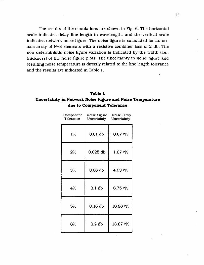
The results of the simulations are shown in Fig. 6. The horizontal
scale indicates delay line length in wavelength, and the vertical scale
indicates network noise figure. The noise figure is calculated for an on-
axis array of N=8 elements with a resistive combiner loss of 2 db. Thenon deterministic noise figure variation is indicated by the width (i.e.,
thickness) of the noise figure plots. The uncertainty in noise figure and
resulting noise temperature is directly related to the line length toleranceand the results are indicated in Table 1.
Table 1
Uncertainty in Network Noise Figure and Noise Temperature
due to Component Tolerance
Component Noise Figure Noise Temp.Tolerance Uncertainty Uncertainty
1%
2%
3%
4%
5O/o
0.01 db
0.025 db
0.06 db
0.1 db
0.16 db
0.67 OK
1.67 OK
4.03 OK
6.75 OK
10.88 OK
6% 0.2 db 13.67 OK

17
The significance of this result is that if the delay line lengths for this
array could not be determined for each beam angle position to an
accuracy tolerance better than the values indicated in the table, thenetwork alone would limit the radiometer sensitivity to the temperatures
indicated. The situation gets worse for greater tolerance variations. For
this reason it is very important to use delay line elements with extremely
repeatable characteristics.
rrl. Phase Shifters
The
allows the
fabricated
switching
itself, can
The most
transmission delay lines create a phase shift function that
antenna beam to be electrically steered. Phase shifters can be
in a variety of configurations, but generally require the use of
elements to change the amount of phase delay. The delay,
be generated using transmission lines or reactance devices.
common switching element used is a PIN diode. The noise
generated by the diode will vary, depending upon the state the switch is
in. The resistance of the diode will vary from a low value in the forward
bias, or 'on' state, to a very high value in the reverse bias or 'off' state.
Since the switch is fundamental to phase shift networks it is important
to understand it's noise characteristics. In this section the noise
performance of three phase shift implementations is investigated. The
phase shifters are fabricated in microstrip using a commercial PIN diode
(MA47899-030). This diode is not necessarily the best diode to use, but is
typical of devices commonly employed in phase shifters. The noise
performance of the phase shifters is typical of experimentally obtained
results.
The three phase shift implementations investigated consist of one
reflection design and two transmission type (switched-line and loaded-
line) phase shifters. The phase shifters were designed to operate at a
center frequency of 4 GHz and were fabricated in microstrip using an
alumina (AL203) substrate. The reflecUon phase shifter uses a hybrid 90 °
coupler in order to operate as a two-port device. All three phase shifters
were designed to provide one bit 45 ° phase shift.

18
The equivalent circuit for the PIN diode is shown in Fig. 7. The
equivalent circuit is applicable for both forward and reverse bias states.The equivalent circuit can be used for other PIN diodes by determination
of the equivalcnt circuit parameters, which can be established by
parameter extraction techniques from measured data. The phase shiftercircuits are shown in Figs: 8a, 8b, and 8c, for the reflection-type,
switched-line, and loaded-line phase shifters, respectively. The RF
performance of the three phase shifters are shown in Figs. 9a, 9b, and
9c, respectively, for the three phase shifters. The RF performance isshown for a frequency band extending from 3 GHz to 5 GHz. The lefthand side vertical scale indicates the return loss and insertion loss for
the phase shifters, and the right-hand side vertical scale indicates the
phase shift angle and noise figure. The RF performance characteristicsfor the three phase shifters are summarized in the following tables.
Table 2
RF Performance of the Three Phase Shifters
Phase
Shifters
Switched-
Line
Loaded-
Line
Reflection-
Type
BW(%)
20.0
11.0
6.8
RL°(db)
-34
-5O
-38
RL l{db)
-.36
-43
-32
ILo{db)
-0.193
-0.020
-0.138
IL 1 (db)
-0.194
-0.082
-0.287

19
CMP4L
o
L-Lp nH
CMP1 k 1=0
spdtk 1 0 3
kl-1
MA47892-109 CMP6EQUATIONCj=I R
EQUATION R{=0.4
EQUATION Rr=O.5
EQUATION [email protected]
EQUATION Cp=8.88
EQUATION Lp=O
CMP5
C
)tC=Cp pF
CMP2
R
R=Rf OH
-t-O
t,..
rv CMP3rv C
)tc-cj pF
CMP7
L
L=Lint nH
Fig. 7 PIN Diode Equivalent Circuit

2O
Table 3
Noise Figure Performance of the Three Phase Shifters
Phase Shifter
Switched-
Line
Loaded-Line
Reflection-
Type
NFo{db)
Center
0.192
0.020
0.137
NF 1 (db)
Center
0.192
0.082
NF°(db)
Max
0.204
0.024
0.284 0.142
NF 1{db)
Max
0.196
0.112
0.287
In Tables 2 and 3 the ,o, and ']' correspond to the two states of the
phase shifter bit. The percent bandwidth is defined as the range of
frequencies with phase shift error less than 10 ° and return loss less than
-20 db.
As indicated in the Figs. 9a, 9b, and 9c and summarized in the
tables it is seen that the loaded-line phase shifter has superior noise
performance over an acceptable bandwidth. The switched-line phase
shifter has a considerably larger bandwidth, but the noise figure
throughout the band is significantly higher. The reflection-type design
provides the least desirable performance ....
The offset between the noise figure values at different positions of
the phase shift angle is an important consideration. In a phased array
application the offset results in uncertainty in the noise figure of the
network and serves to degrade system sensitivity in much the same way

21
OiPlll
SUUST,-dG88G-T .... E3_.6
•._T :%66 mill _!Ct_l_)-5.6e7
H,,,I6 ed I _ um
,L TFV'4I)-O.08C2
o,p7NSl'l.
21_,,,_51_ mi,_-u35b rail
_G_
(_NP4t
_6b-9.95 EQUATION
quir tb-_. $$OeO/4e)/sqrt (9.G)/4N !80/2.54_ | HOVkbkb-l.O0 EOL_TION
[(IJ_TIOH Lshort-OS.B
EOUQTIOH Lm-B,UEI
011'1i 01PIZ
SU'BST,,dGDBE oqr$ SLJES'I",,dG66G m,4_Hl,,,v5Ob railI(2_5b millS"ll. Hl_5b m_81_ rail
L_ Impic]uartbmi I Im_Lbumil
__ _ 14,.u35bmi I H-wS_ rail
_lDST'dGl_m3Sb mH!l,-uSgb rail
L'mquurtb mi I _JDST-cIGOB5H'-_5b mi I
OqF'15
-...---..---...Ea--- ---_]
pinbk:
,u | m
EQU_TION_=I
QGROUND
$RGROUNB
_JEST=d688£ _/
L.d.Jhort @G_OUN]3
kl_ mi I
04P5|
JI,_=dGO86
C-L_hor t @Gi_OUND
Fig. 8a Reflection-Type Phase Shifter

22
mgm.
I,Br+3 m
T"H-16 mi I
HSSLmSTR_T[
5UBST-sI h i IER-S. 6 '---MUR- I _ _
CONI)-I.6E+396 r';
TAND-B.O
Switched-Line Phase Shi.Fter
o4P't7 o_!
oe'J! SUBST slBmil l lH-.i milEOUATION LI=IBB(731(20Blr_tm_ L=LI mil L.r.JEOUATION L2-IBB(BTG(2BBB H=uz milEOUATIONua=9.85
EOUATION ws,,wl ] '._:_..Imi_l] pi.i_
EOUATIONk l,,r _OUATIONk3-_|
'FLLEIUATION ,'B _'_ mmJ|
EQUATIONl,,_-l-r _ EOUATIONk4-I-r
:'"L'I :"21_-" _-"
W-vb mi I _ ot_|5UBST-s Ih i I
5UBST=zlSmi I -- -
L-L2 mi ] "_&m_t
-.. _..,, ;Zi
Fig. 8b Switched-Line Phase Shifter

23
I
HI,l=I.8[+3 m
! ,!_}"T'
H,',I B rail,l
(:NP1I,ISSUL_"R_ITE
SUBST-= IBmi 1
ER-9. G
NOR- 1COND-1. BE+3B6ROUGH-{} um
TAND-8.{}
(_lS
SUBST-: 18mi I (:_Hl=w: mi I H2-wa mi 1 I_TL
_ SUBST,,= l_i IIm,illa mi I
I1":
EQUATION k
. .@._,!
..j ul .,4 "l-
1,,1
• pinbkl]
AGROUND
Loaded-line 45'Phase ShiTter Bit
EOUATION LA= 100<2BB. B<2880
EOUATION LB= 1B8<433.0( 2888
EOUATIONXA-I< 11.61<28
EQUATION HB=(}. 1( 1.41<28
EOUATION w:-9.95
OVpllllb-rE
SUBST-= IBmiI
Nl-wa railX;_'w: rail
Jia-wa/4 rail
r
II
i _
I l
._1-1.
EOUATION ,?-I
•__ I:_
pink2
II
AGROUND
Fig. 8c Loaded-Line Phase Shifter

24
RL IL I
I
4
----] Ph.Shift NF98 I
PICI
SI
8
Fig. 9a Reflection-Type Phase Shifter Performance

25
RL IL
8 B 1 TL
"_'_ 7",,I
\/" I__i_ 4
,/
.... ! /'
/ i t
98
,Cl
5
NF
0.5
0
f(GHz)
Fig. 9b Loaded-Line Phase Shifter Performance

26
RL IL0 8
iI
NF1
f(GHz)
Fig. 9c Switched-Line Phase Shifter Performance
27
as discussed for the tolerance considerations. The switched-line phase
shifter appears to have the most desirable characteristics in this regard.
IV. Conclusions
The noise figure performance of various delay line networks
fabricated from microstrip lines with varying number of elements was
investigated using a computer simulation. The effects of resistive losses
in both the transmission lines and power combiners was considered. In
general, it is found that an optimum number of elements exists,
depending upon the resistive losses present in the network. Small
resistive losses are found to have a significant degrading effect upon the
noise figure performance of the array. Extreme stability in switching
characteristics is necessary to minimize the non deterministic noise of
the array. For example, it is found that a 6% tolerance on the delay line
lengths will produce a 0.2 db uncertainty in the noise figure which
translates into a 13.67 °K temperature uncertainty generated by the
network. If the tolerance can be held to 2% the uncertainty in noise
figure and noise temperature will be 0.025 db and 1.67 °K, respectively.
Three phase shift networks fabricated using a commercially
available PIN diode switch were investigated. Loaded-line phase shifters
are found to have desirable RF and noise characteristics and are
attractive components for use in phased-array networks.

28
Switched-Beam Radiometer Front-End Network Analysis
Addendum
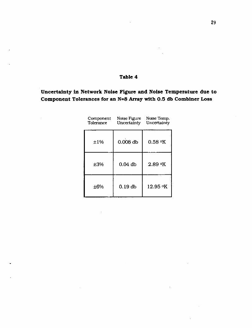
After submission of this report some additional calculations were
performed. The purpose of these calculations was to investigate the
uncertainty in the noise figure and noise temperature for a combiner
structure that had lower loss than the combiner previously investigated
and reported. The original calculations are described starting on page 13
in the Monte Carlo Tolerance Simulation section. The original
calculations were performed for an N=8 combiner array with 2 db
combiner loss. "These calculations resulted in the the uncertainty values
presented in Table I on page 16. As indicated in Table 1 the noise
temperature uncertainty varies from 0.67 °K for 1% line length tolerance
to 13.67 °K for 6 % line length tolerance.
The new calculations reported in this Addendum were performed
for the identical combiner array, except that the combiner loss was
reduced to 0.5 db. The results are presented in Table 4.
As indicated in Table 4, the decrease in the combiner loss from 2
db to 0.5 db produces a slight reduction in the uncertainty in the
network noise figure and noise temperature. However, the reduction is
not in proportion to the combiner loss reduction. For example, for 1%
line length tolerance the noise temperature uncertainty is reduced from
0.67 °K to 0.58 °K, and for 6% tolerance the noise temperature
uncertainty is reduced from 13.67 °K to 12.95 °K.
These calculations indicate that the line length variation due to
the tolerances is far more significant in determination of the network
noise temperature uncertainty than is the actual magnitude of the
combiner loss. Since the uncertainty in the noise temperature cannot be
removed from the system noise temperature by calibration, it represents
a lower limit to radiometer sensitivity. It is believed that this issue is
fundamental to understanding the use of switched-beam networks in
radiometry. Although this study only considered a simple combiner
network the physical principles revealed are significant and additional
work should be performed to more clearly understand the problem.
29
Table 4
Uncertainty in Network Noise Figure and Noise Temperature due to
Component Tolerances for an N=8 Array with 0.5 db Combiner Loss
Component Noise Figure Noise Temp.Tolerance Uncertainty Uncertainty
+1%
±3%
0.008 db
0.04 db
0.58 oK
2.89 oK
±6% 0.19 db 12.95 oK

Form Approved
REPORT DOCUMENTATION PAGE OH8No070 -0,aam ,, i i..
Putdic reDortlng burden for this collecti0n of reformation ,s est,mate_ to average, hour r_er response, incluClin,g the time for rew ewlncj ,n.$truct,OnS, searchlrngnetxlstL_g :sa_.c_Oot_r_
atherl and maintaining the data needed, and comptet=ng and rev_ew,ng the collection ot _nTormatlon .ena comments re_armng tn_s Duraen estimate or .a y o_ .... _ = __cgoallectio_Jnof information, including suggestions for reducing thts burden, to Wash=ngtOn HeadQuarters Services. ulrec_orate tot Information uperat=ons ana _epor_s, i=]_ JeT_e._un
Davis Highway. Suite 1204, Arlington, VA 22202-4]02, and to the Office of Management and Budget, Paperwork Reduction Project (0704-0188). Washington. DC 20503.
I. AGENCY USE ONLY (Leave blank) 2. REPORT DATE 3. REPORT TYPE AND DATES COVERED
4.TITLEAND SUBTITLE
Switched-Beam Radiometer
June 1994
Front-End Network Analysis
6.. AUTHOR(S)
R. J. Trew and G. L. Bilbro
7. PERFORMING ORGANIZATION NAME(S) AND ADDRESS(ES)
North Carolina State University
Department of Electrical and Computer Engineering
Raleigh, NC 27695-7911
9. SPONSORINGIMONITORINGAGENCYNAME(S)ANDADDRESS(ES)National Aeronautics and Space Administration
Langley Research Center
Hampton, VA 23681-0001
Contractor Report5.FUNDINGNUMBERS
G NAG1-943
WU 505-64-12-02
B. PERFORMING ORGANIZATIONREPORT NUMBER
10. SPONSORING/MONITORINGAGENCY REPORT NUMBER
NASA CR-194922
11. SUPPLEMENTARY NOTES Final ReportTrew: Case Western Reserve University, Dept. of Elect. Eng. and Applied Physics,Cleveland, OH; Bilbro: North Carolina State University, Dept. of Elect. and
Computer Eng., Raleigh, NC Langley Technical Monitor: C. P. Hearn12b. DISTRIBUTION CODE• 1
12a. DISTRIBUTION IAVAILABILITY STATEMENT
Uncl assi fied-Unl imi ted
Subject Category 32
13. ABSTRACT (Maximum 200 words)
The noise figure performance of various delay-line networks fabricated from microstrip lineswith varying number of elements was investigated using a computer simulatiorL The effects ofresistive losses in both the transmission lines and power combiners were considered. Ingeneral, it is found that an optimum number of elements exists, depending upon the resistivelosses present in the network. Small resistive losses are found to have a significant degradingeffect upon the noise figure performance of the array. Extreme stabilt W in switchingcharacteristics is necessary to minimize the non-determml.Cdc noise of the array. For ,example, it is found that a 6 percent tolerance on the delay-line lengths will produce a 0.2-dbuncertainty in the noise figure which translates into a 13.67°K temperature uncertaintygenerated by the network. If the tolerance can be held to 2 percent, the uncertainty in noisefigure and noise temperature will be 0.025 db and 1.67°K. respectively. Three phase shiftnetworks fabricated using a commercially available PIN diode switch were investigated.Loaded-line phase shifters are found to have desirable RF and noise characteristics and areattractive components for use in phased-array networks.
ii
14. SUBJECT TERMS
switched-beam, noise figure performance, microstrip, resistive
losses, phase-shift networks
17. SECURITYCLASSIFICATION18. S'ECURITYCLASSIFICATIONOF REPORT OFTHISPAGE
Unclasslf_ed , UnclassifiedNSN7540-01-280-5500
19. SECURITY CLASSIFICATIONOF ABSTRACT
15. NUMBER OF PAGES
3116. PRICE CODE
A0320. LIMITATION OF ABSTRACT
Standard Form 298 (Rev. 2-89)Prescribed by ANSI Std. Z_I.III
2gB-102


![The Advanced Microwave Radiometer – Climate Quality (AMR-C) … · 2018-03-08 · Microwave Radiometer (HRMR) [6] and a Supplemental Calibration System (SCS). The radiometer channels](https://img.pdfslide.net/doc/110x75/5f35db4eb6ba30245530385e/the-advanced-microwave-radiometer-a-climate-quality-amr-c-2018-03-08-microwave.jpg)