Embed Size (px)
Citation preview

Switched Capacitor Circuits
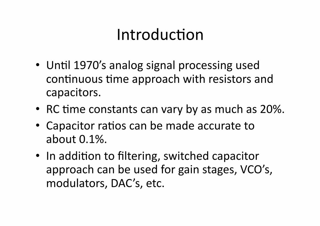
Introduc3on
• Un3l 1970’s analog signal processing used con3nuous 3me approach with resistors and capacitors.
• RC 3me constants can vary by as much as 20%. • Capacitor ra3os can be made accurate to about 0.1%.
• In addi3on to filtering, switched capacitor approach can be used for gain stages, VCO’s, modulators, DAC’s, etc.
Introduc3on
• A Switched Capacitor (SC) circuit is built of OPAMPs, switches, capacitors, and clocks.
• The OPAMPs used will have finite dc gain, finite unity gain frequency (GBW), slew rate, and dc offset.
• The capacitors are generally parallel plate capacitors and should be correctly modeled.
• The ON and OFF resistances and parasi3c capacitances of the switches are important.
• The 3ming of the clocks is very important and non-‐overlapping clocks may be required.

Introduc3on
Phi1 Phi2
V1 V2

Introduc3on
• C1 is charged to V1 and V2 each clock period. • The change in charge over one clock period ΔQ1 is given by,
• Then,
€
ΔQ1 = C1 V1 −V2( )
€
Iavg =C1 V1 −V2( )
T
Req =TC1
=1C1 f s
Technology
• Capacitors can be realized by four different techniques; metal-‐n+, metal poly, poly-‐poly, and metal-‐metal.
• Metal-‐n+ uses the gate oxide. Hence, large capacitance in a small area. However, voltage dependence and substrate noise.
• Metal-‐poly is more linear, but has large parasi3cs.

Technology
• Poly-‐poly is also quite good, but not available in many technologies. Also, large parasi3c capacitances.
• MIM (Metal-‐Insulator-‐Metal) present only in modern technologies. Typically the best choice.
• You can even build your own ver3cal capacitors. However, matching will not be that good.
Technology
• In order to match capacitors, the Area/Perimeter ra3os should be kept the same.
• Also, use symmetry and common centroid type layouts.
• Be careful about local and global type random errors.
Technology
sweep
impe
danc
e
XXX
0.2 0.4 0.6 0.8 1.0 1.2 1.4 1.6 1.8 2.0 2.2V
0.0
5.0
10.0
15.0
20.0
kohm (v(3) - v(4))/i(vdum)

Technology
sweep
impe
danc
e
XXX
0.0 0.5 1.0 1.5 2.0 2.5 3.0 3.5V
1
2
3
4
5
6
7
8
9
kohm (v(3) - v(4))/i(vdum)

Technology
sweep
impe
danc
e
XXX
0.0 0.5 1.0 1.5 2.0 2.5 3.0 3.5V
1.8
2.0
2.2
2.4
2.6
2.8
kohm (v(3) - v(4))/i(vdum)
Technology
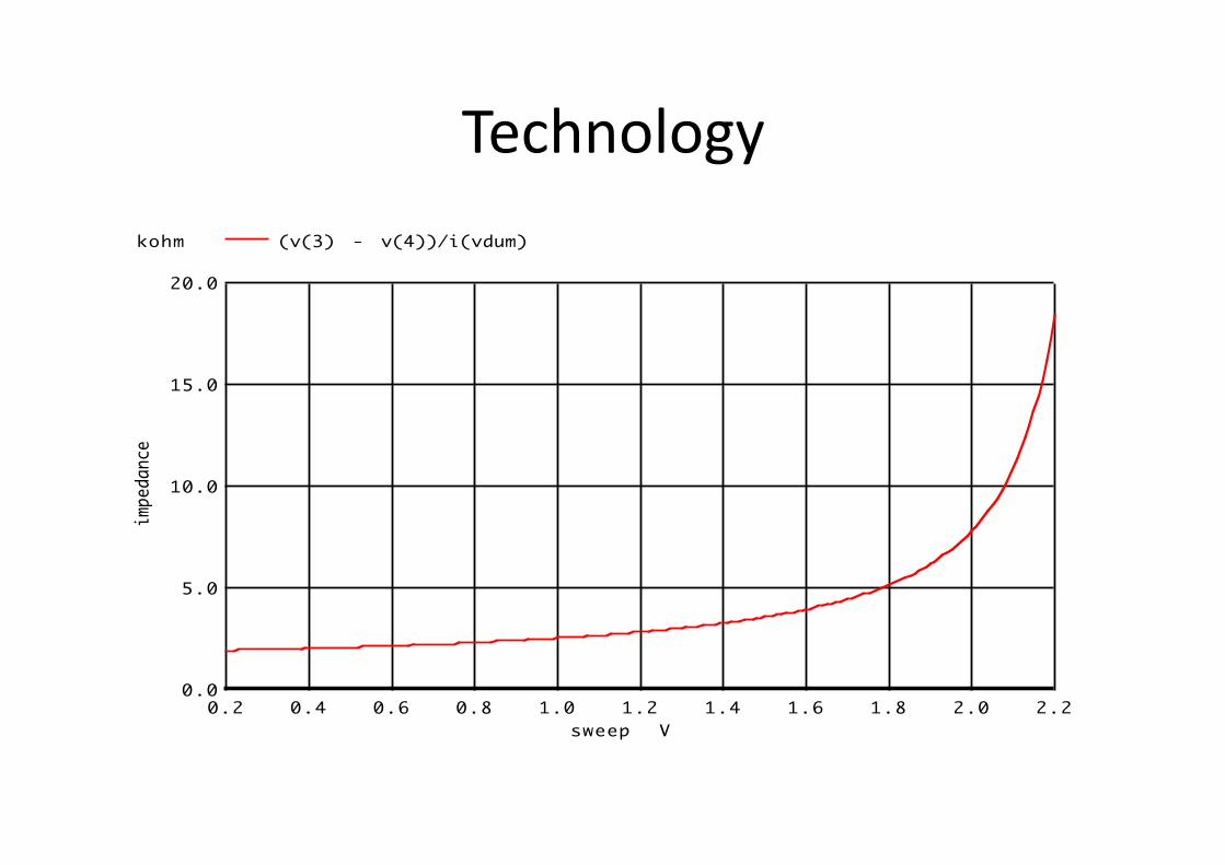
• The first curve is the ON resistance of a single NMOS (W=1µm L=0.35µm).
• The second curve is the ON resistance of a transmission gate with iden3cal NMOS and PMOS devices.
• The final curve is the ON resistance of a transmission gate with a PMOS device of dimension W=3.5µm L=0.35µm.
Technology
• For small supply voltages, the two peaks come together and the resistance is not reduced properly.
• Now, let us decrease the supply voltage to 2.5V from 3.3V.
• Finally, we will decrease it to 0.8V. • Take the most symmetric curve (with the larger PMOS device).

Technology
sweep
impe
danc
e
XXX
0.0 0.5 1.0 1.5 2.0 2.5V
2.0
2.5
3.0
3.5
4.0
4.5
kohm (v(3) - v(4))/i(vdum)

Technology
sweep
impe
danc
e
XXX
0.2 0.4 0.6 0.8 1.0 1.2 1.4 1.6 1.8V
2.0
4.0
6.0
8.0
10.0
12.0
14.0
16.0
kohm (v(3) - v(4))/i(vdum)

Simple Calcula3ons
• Let us now calculate the effect of RON on the opera3on of the circuit.
• The resistance creates a simple RC network with the capacitance of the SC circuit.
• One can easily write its behavior.
€
Vout =Vin 1− exp −tRC
⎛
⎝ ⎜
⎞
⎠ ⎟
⎛
⎝ ⎜
⎞
⎠ ⎟
ts = RC ln 1ε( )
Simple Calcula3ons
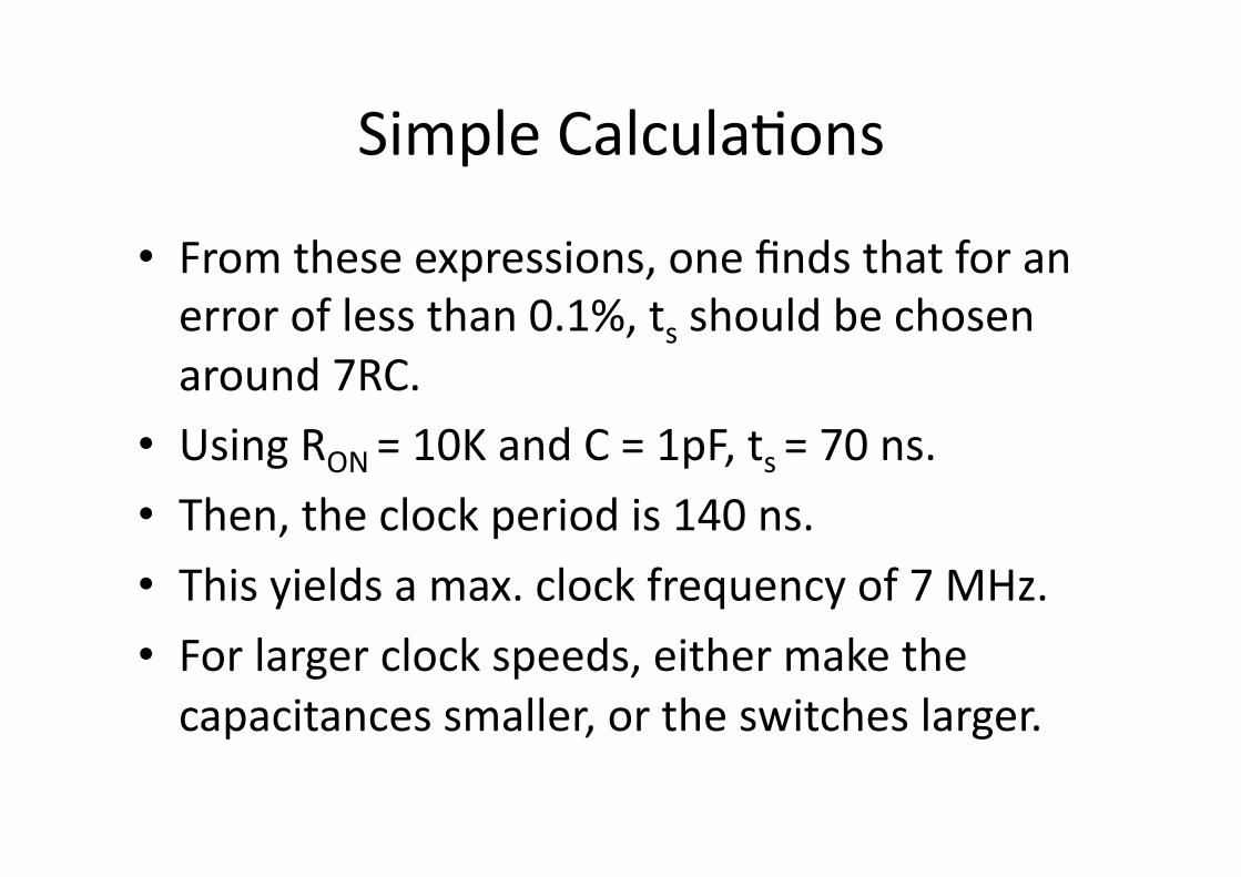
• From these expressions, one finds that for an error of less than 0.1%, ts should be chosen around 7RC.
• Using RON = 10K and C = 1pF, ts = 70 ns. • Then, the clock period is 140 ns. • This yields a max. clock frequency of 7 MHz.
• For larger clock speeds, either make the capacitances smaller, or the switches larger.

Simple Calcula3ons
• The leakage currents through the OFF switches also dictate a minimum frequency.
• For our technology, this frequency is on the order of a few Hz at room temperature although it increases exponen3ally with temperature.

Simple Calcula3ons
• Clock feedthrough is also important. • The clock signals couple to the capacitors over the overlap capacitances.
• For W = 3µm and L = 0.7µm, Cov = 1fF.
• This creates about 3mV error in the stored voltage.
• Note however that this error is at the clock frequency and its harmonics.

Simple Calcula3ons
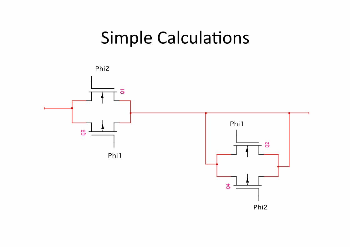
• Charge redistribu3on is also important. • The charge stored in the channel disappears when the transistor is switched OFF.
• For the same transistor, Q is about 6fC.
• If it divides into two equal por3ons (for source and drain), it creates 3mV error on the 1pF external capacitors.

Simple Calcula3ons
• One solu3on to charge redistribu3on is to increase the capacitances. However, this will also increase the area and the power and decrease the speed.
• Another op3on is to insert a dummy switch of half size working at the opposite phase. This is successful if the charge is split into two equal por3ons.
Simple Calcula3ons
Phi2
Phi1
Phi1
Phi2
Simple Calcula3ons
• If the charge is not split equally, this might even may things worse.
• How the charge splits is a complex func3on of the rise and fall 3mes of the clocks, the clock jijer, and the capacitances on each side of the switch.
• For steep rise and fall 3mes, the capacitance ra3os on either side has less effect.
Simple Calcula3ons
• Another op3on to reduce the error is to use a fully differen3al approach.
• Also, using iden3cal NMOS and PMOS devices helps.

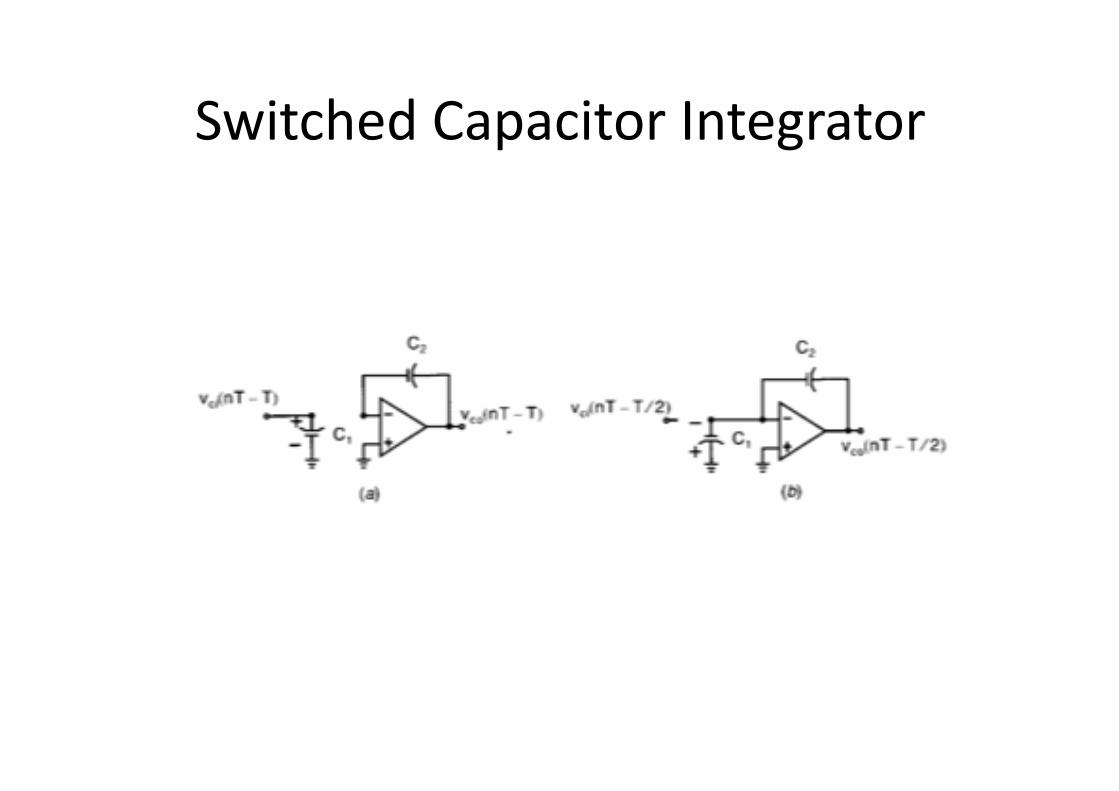
Switched Capacitor Integrator
Switched Capacitor Integrator
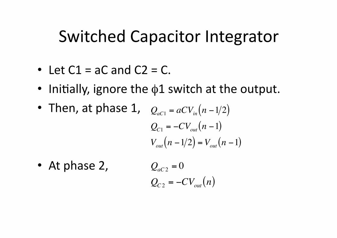
• Let C1 = aC and C2 = C. • Ini3ally, ignore the φ1 switch at the output. • Then, at phase 1,
• At phase 2, €
QaC1 = aCVin n −1 2( )QC1 = −CVout n −1( )Vout n −1 2( ) =Vout n −1( )
€
QaC 2 = 0QC 2 = −CVout n( )

Switched Capacitor Integrator
• Using charge conserva3on,
• This equa3on is valid if sampling is performed at φ2.
• If φ1 is preferred for sampling,
€
QaC 2 +QC 2 =QaC1 +QC1
−CVout n( ) = aCVin n −1 2( ) −CVout n −1( )
€
−CVout n( ) = aCVin n −1( ) −CVout n −1( )

Switched Capacitor Integrator
• The first equa3on becomes in the z-‐domain
• The second equa3on becomes
€
CVout = z−1CVout − z−1 2aCVin
Vout
Vin
= −a z−1 2
1− z−1
€
CVout = z−1CVout − z−1aCVin
Vout
Vin
= −a z−1
1− z−1
Switched Capacitor Integrator
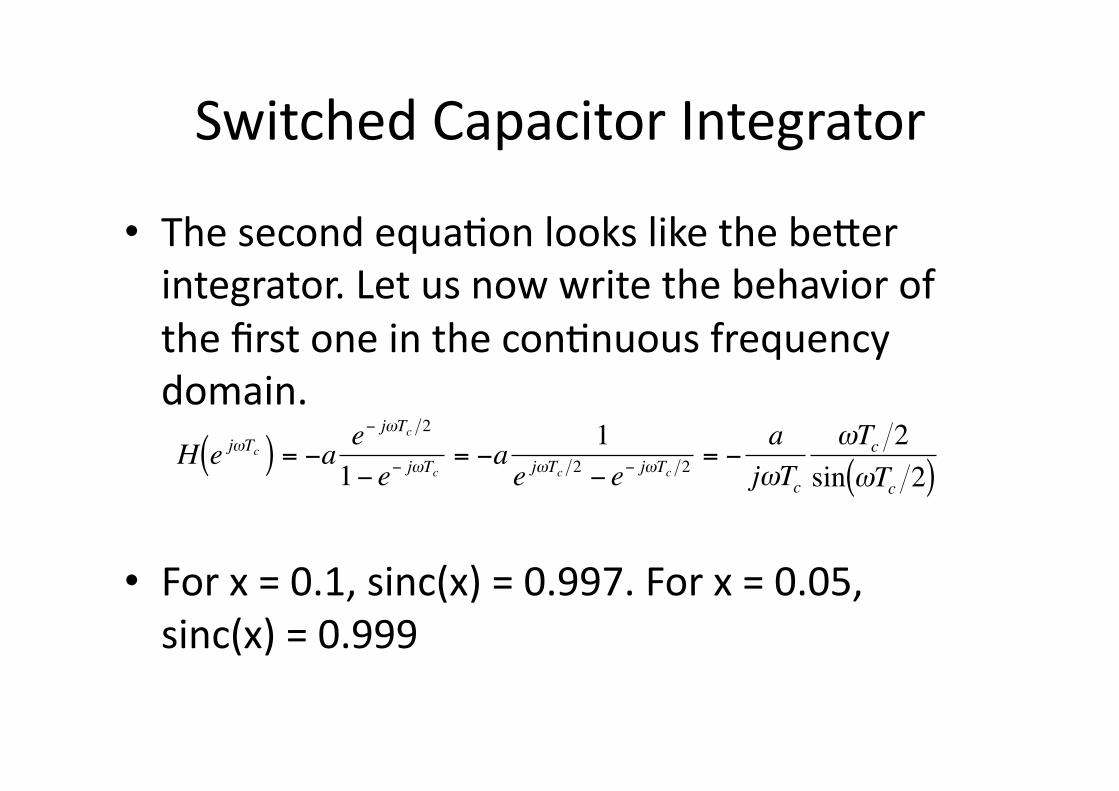
• The second equa3on looks like the bejer integrator. Let us now write the behavior of the first one in the con3nuous frequency domain.
• For x = 0.1, sinc(x) = 0.997. For x = 0.05, sinc(x) = 0.999
€
H e jωTc( ) = −a e− jωTc 2
1− e− jωTc= −a 1
e jωTc 2 − e− jωTc 2= −
ajωTc
ωTc 2sin ωTc 2( )

Switched Capacitor Integrator
• The second equa3on becomes in the frequency domain,
• This equa3on has a phase error in addi3on to the magnitude error.
• The phase error can create instabili3es in higher order systems.
€
Vout
Vin
= −ajωTc
ωTc 2sin ωTc 2( )
e− jωTc 2

Switched Capacitor Integrator
• There are stray capacitances at the input. These are typically connected to ground. Hence they are shorted out.
• There are also stray capacitances also in the feedback. – If the stray capacitance is connected to the nega3ve input of the OPAMP, it couples noise.
– If it is connected to the output, it changes the load capacitance.

Switched Capacitor Integrator
• Moreover, the source and drain capacitances of the switches are added to the input capacitance, causing 5 -‐ 10% error.
• Thus, this integrator is rarely used. • Instead, a stray insensi3ve integrator should be preferred.

Switched Capacitor Integrator

Switched Capacitor Integrator
• Capacitor C1 is now floa3ng. • Similar func3ons are carried out during the two phases.
• During phase 1, C1 is charged to the input voltage.
• During phase 2, it is discharged to zero, forcing the charge to C2.
Switched Capacitor Integrator

Switched Capacitor Integrator
• During phase 1 (figure a), the lel side of the capacitor is charged posi3vely. Its right side is nega3ve.
• During phase 2 (figure b), it is applied to an inver3ng configura3on.
• Therefore, the net result is that it is a non-‐inver3ng integrator.
Switched Capacitor Integrator
• Now, look at phase 1 (figure a) more closely. • The stray capacitance to the lel of C1 is charged to the input voltage through a low impedance node.
• Thus, its charge does not affect the charge on C1.
• The capacitance to the right is shorted to ground. Hence, no effect.

Switched Capacitor Integrator
• During phase 2 (figure b), the parasi3c capacitor to the lel of C1 is shunted to ground.
• Its charge obtained during phase 1 disappears into ground.
• The parasi3c capacitor on the right is now connected to the nega3ve terminal of the OPAMP and hence to virtual ground.
• This way, one can choose the integrator capacitances smaller, saving power and speed.

Switched Capacitor Integrator

Switched Capacitor Integrator
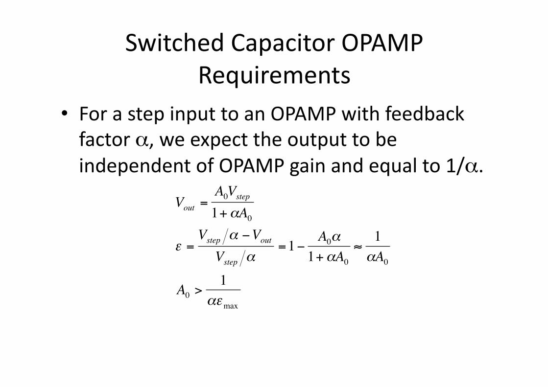
Switched Capacitor OPAMP Requirements
• For a step input to an OPAMP with feedback factor α, we expect the output to be independent of OPAMP gain and equal to 1/α.
€
Vout =A0Vstep
1+αA0
ε =Vstep α −Vout
Vstep α=1− A0α
1+αA0≈1αA0
A0 >1
αεmax
Switched Capacitor OPAMP Requirements
• For a maximum error of 0.05%, the required gain is 5000 – 10000.
• The sejling 3me is also quite important.
• Let us call the error from the sejling 3me the dynamic error εD.
• For a devia3on of 0.1%, about 7 3me constants are necessary.
• Let us look at this more analy3cally
Switched Capacitor OPAMP Requirements
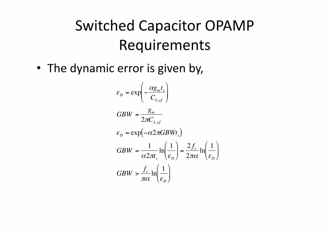
• The dynamic error is given by,
€
εD = exp −αgmtsCL,ef
⎛
⎝ ⎜ ⎜
⎞
⎠ ⎟ ⎟
GBW =gm
2πCL ,ef
εD = exp −α2πGBWts( )
GBW =1
α2πtsln 1εD
⎛
⎝ ⎜
⎞
⎠ ⎟ =
2 fc2πα
ln 1εD
⎛
⎝ ⎜
⎞
⎠ ⎟
GBW >fcπαln 1εD
⎛
⎝ ⎜
⎞
⎠ ⎟
Switched Capacitor OPAMP Requirements
• The term ln(1/εD) is about 7 for 0.1%, but 7.6 for 0.05%.
• For α unity, 2.4*fc would be enough. • Typically, large a values are not present in switched capacitor circuits. Thus, the GBW is chosen about 3 3mes the clock period.
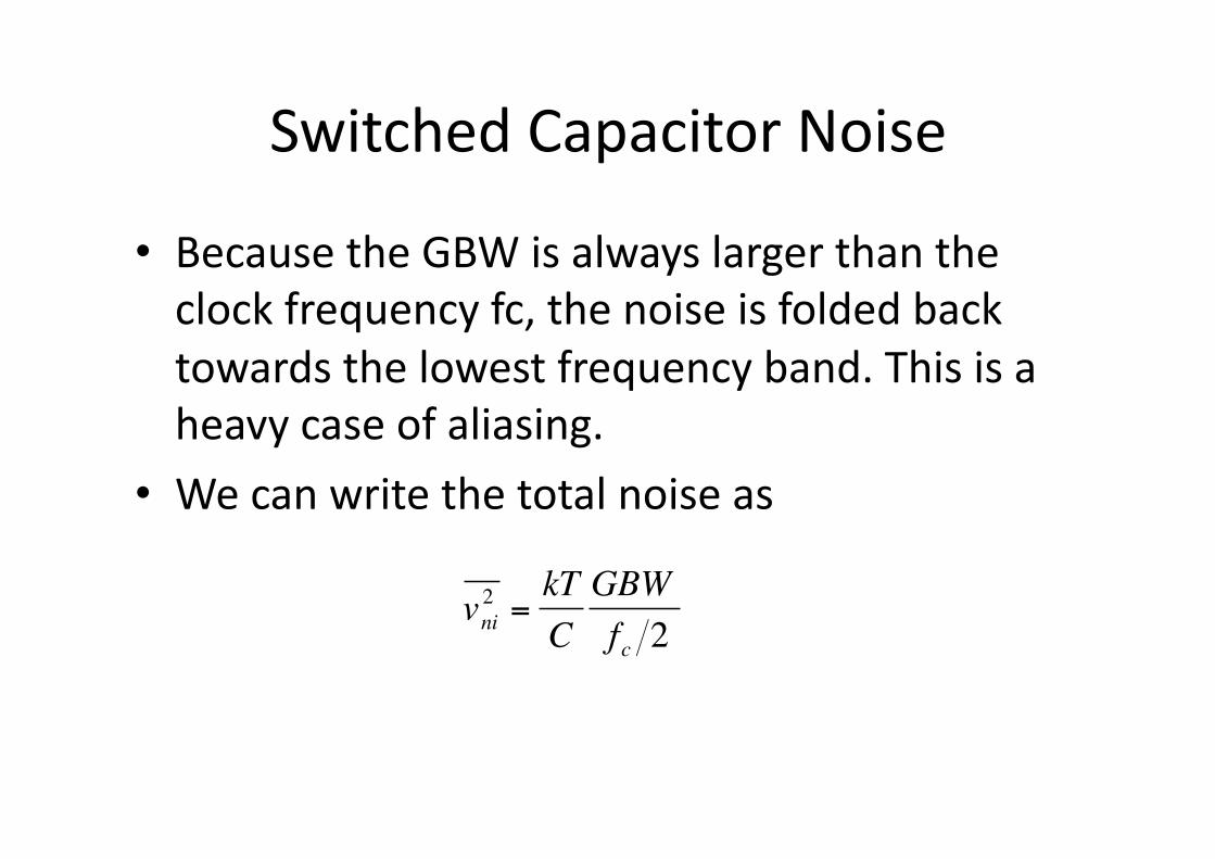
Switched Capacitor Noise
• Because the GBW is always larger than the clock frequency fc, the noise is folded back towards the lowest frequency band. This is a heavy case of aliasing.
• We can write the total noise as
€
vni2 =
kTCGBWfc 2
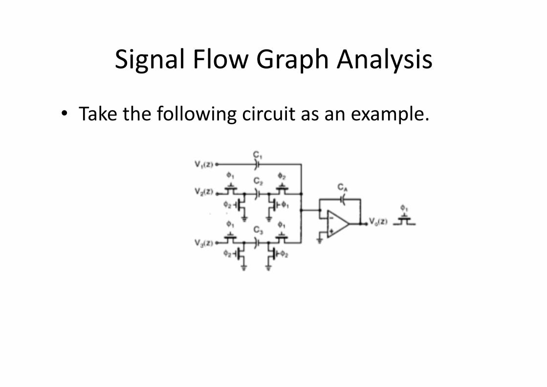
Signal Flow Graph Analysis
• Take the following circuit as an example.
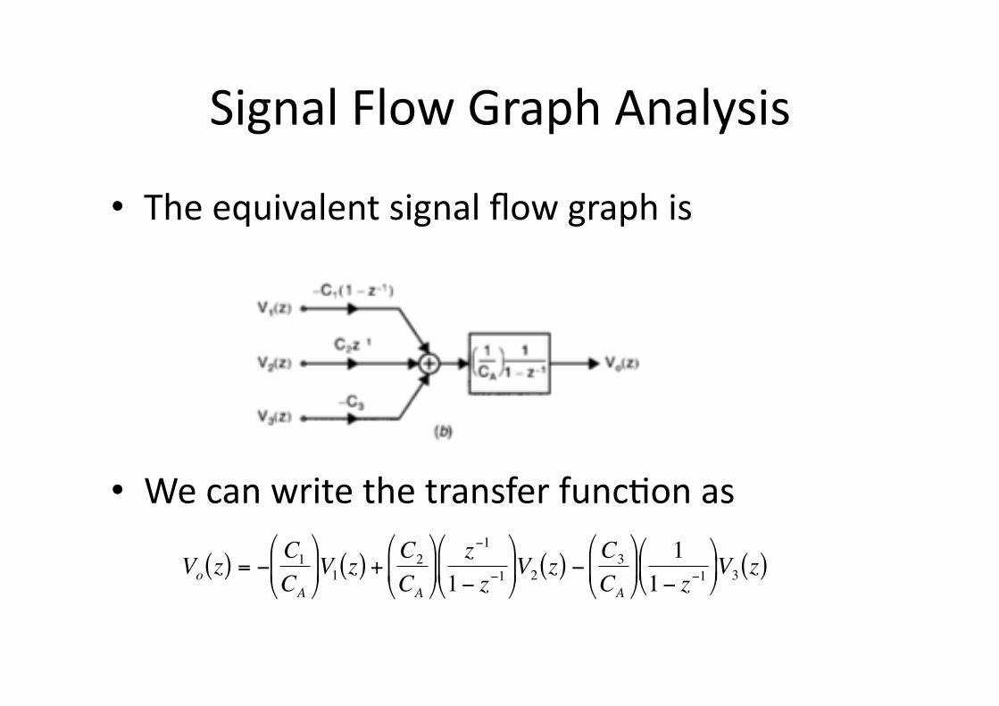
Signal Flow Graph Analysis
• The equivalent signal flow graph is
• We can write the transfer func3on as
€
Vo z( ) = −C1CA
⎛
⎝ ⎜
⎞
⎠ ⎟ V1 z( ) +
C2
CA
⎛
⎝ ⎜
⎞
⎠ ⎟
z−1
1− z−1⎛
⎝ ⎜
⎞
⎠ ⎟ V2 z( ) − C3
CA
⎛
⎝ ⎜
⎞
⎠ ⎟
11− z−1⎛
⎝ ⎜
⎞
⎠ ⎟ V3 z( )
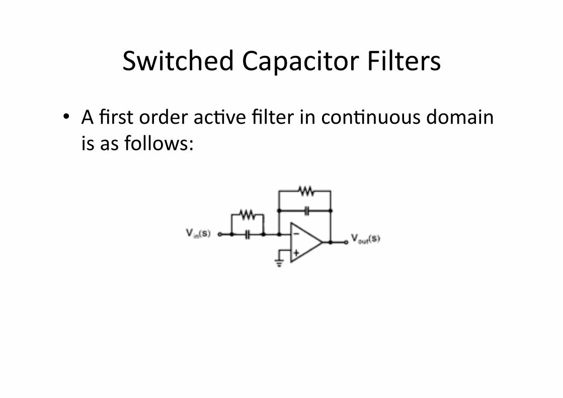
Switched Capacitor Filters
• A first order ac3ve filter in con3nuous domain is as follows:

Switched Capacitor Filters
• A direct implementa3on of this is as follows:
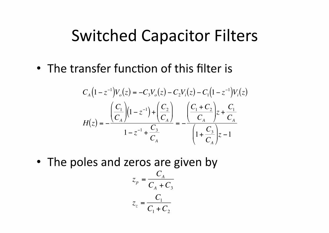
Switched Capacitor Filters
• The transfer func3on of this filter is
• The poles and zeros are given by €
CA 1− z−1( )Vo z( ) = −C3Vo z( ) −C2Vi z( ) −C1 1− z
−1( )Vi z( )
H z( ) = −
C1CA
⎛
⎝ ⎜
⎞
⎠ ⎟ 1− z−1( ) +
C2
CA
⎛
⎝ ⎜
⎞
⎠ ⎟
1− z−1 +C3
CA
= −
C1 +C2
CA
⎛
⎝ ⎜
⎞
⎠ ⎟ z +
C1CA
1+C3
CA
⎛
⎝ ⎜
⎞
⎠ ⎟ z −1
€
zp =CA
CA +C3
zz =C1
C1 +C2
Switched Capacitor Filters
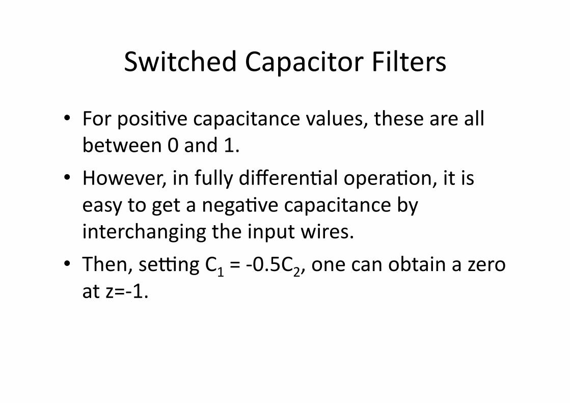
• For posi3ve capacitance values, these are all between 0 and 1.
• However, in fully differen3al opera3on, it is easy to get a nega3ve capacitance by interchanging the input wires.
• Then, sepng C1 = -‐0.5C2, one can obtain a zero at z=-‐1.

Switched Capacitor Filters
• Let us now carry out an exact analysis
• Making ωT<<1, €
H z( ) = −
C1CA
⎛
⎝ ⎜
⎞
⎠ ⎟ z1 2 − z−1 2( ) +
C2
CA
⎛
⎝ ⎜
⎞
⎠ ⎟ z1 2
z1 2 − z−1 2 +C3
CA
z1 2
H e jωT( ) = −j 2C1 +C2
CA
sin ωT2
⎛
⎝ ⎜
⎞
⎠ ⎟ +
C2
CA
cos ωT2
⎛
⎝ ⎜
⎞
⎠ ⎟
j 2 +C3
CA
⎛
⎝ ⎜
⎞
⎠ ⎟ sin
ωT2
⎛
⎝ ⎜
⎞
⎠ ⎟ +
C3
CA
cos ωT2
⎛
⎝ ⎜
⎞
⎠ ⎟
€
H e jωT( ) ≈j C1 +C2 2
CA
⎛
⎝ ⎜
⎞
⎠ ⎟ ωT +
C2
CA
j 1+C3
2CA
⎛
⎝ ⎜
⎞
⎠ ⎟ ωT +
C3
CA
Switched Capacitor Filters
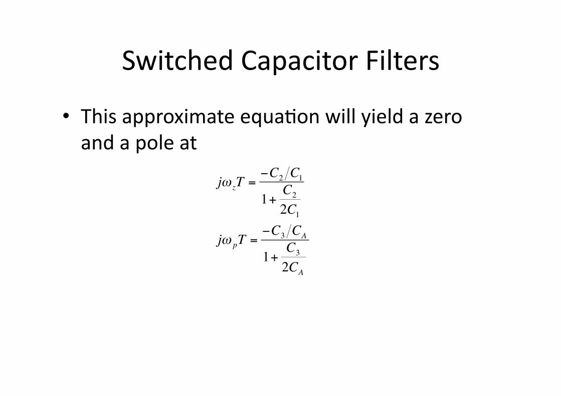
• This approximate equa3on will yield a zero and a pole at
€
jω zT =−C2 C11+
C2
2C1
jω pT =−C3 CA
1+C3
2CA
Switched Capacitor Filters
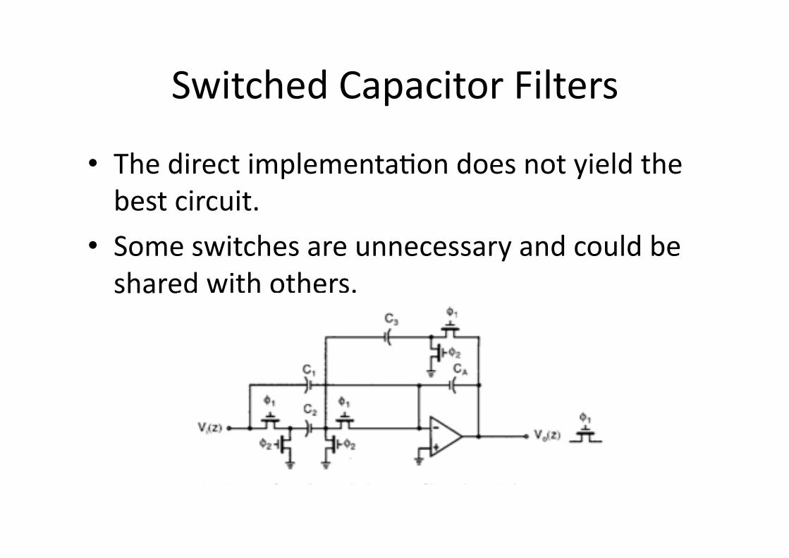
• The direct implementa3on does not yield the best circuit.
• Some switches are unnecessary and could be shared with others.

Switched Capacitor Filters
• Switched capacitor filters should in general be implemented in a fully differen3al fashion.

Switched Capacitor Filters
• One can design more complex filters with the techniques shown above.
• Many higher order filters are designed with the SC technique nowadays.
• However, SC circuits have many more applica3ons.

Differen3al SC Integrator
time
voltage
XXX
0.0 20.0 40.0 60.0 80.0 100.0us
-600
-400
-200
0
200
400
600
mV v(10) v(11)
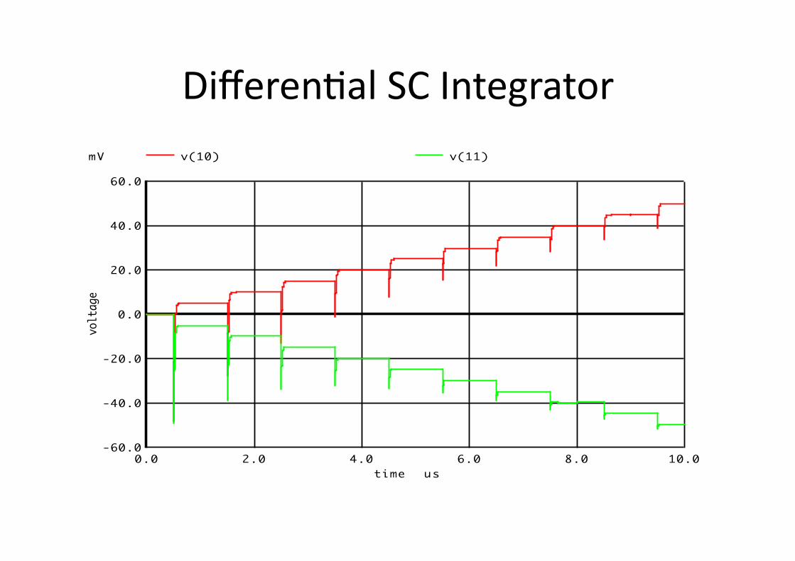
Differen3al SC Integrator
time
volt
age
XXX
0.0 2.0 4.0 6.0 8.0 10.0us
-60.0
-40.0
-20.0
0.0
20.0
40.0
60.0
mV v(10) v(11)
Switched Capacitor Gain Circuits

Switched Capacitor Gain Circuits
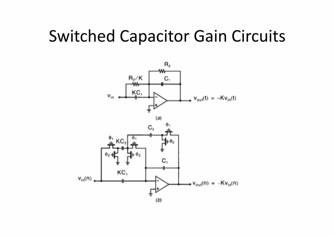
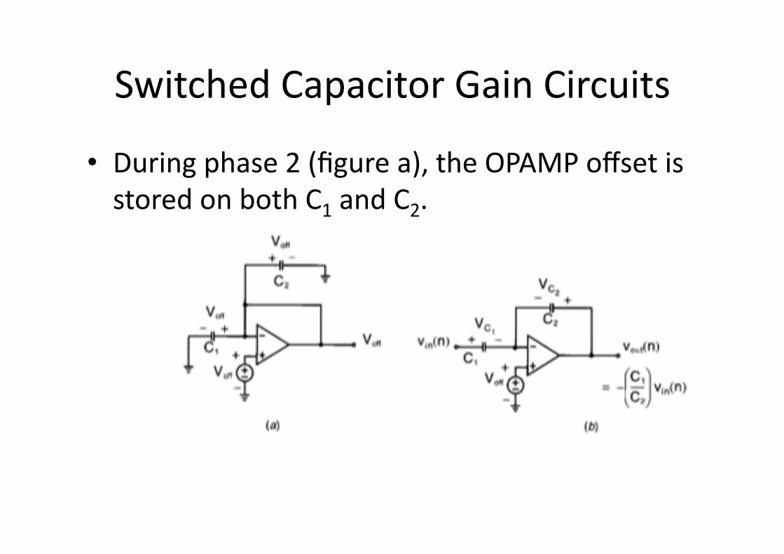
• The following is a resejable gain circuit where OPAMP offset is cancelled.
Switched Capacitor Gain Circuits
• During phase 2 (figure a), the OPAMP offset is stored on both C1 and C2.

Switched Capacitor Gain Circuits
• At the end of phase 1 (figure b), the voltage across C1 is given by VC1(n) = Vin(n) – Voff.
• On the other hand, the voltage across C2 is given by VC2(n) = Vout(n) – Voff.
• Then,
€
ΔQC1 = C1 VC1 n( ) − −Voff( )[ ] = C1Vin n( )
VC 2 n( ) =VC 2 n −1 2( ) − ΔQC 2
C2
Switched Capacitor Gain Circuits
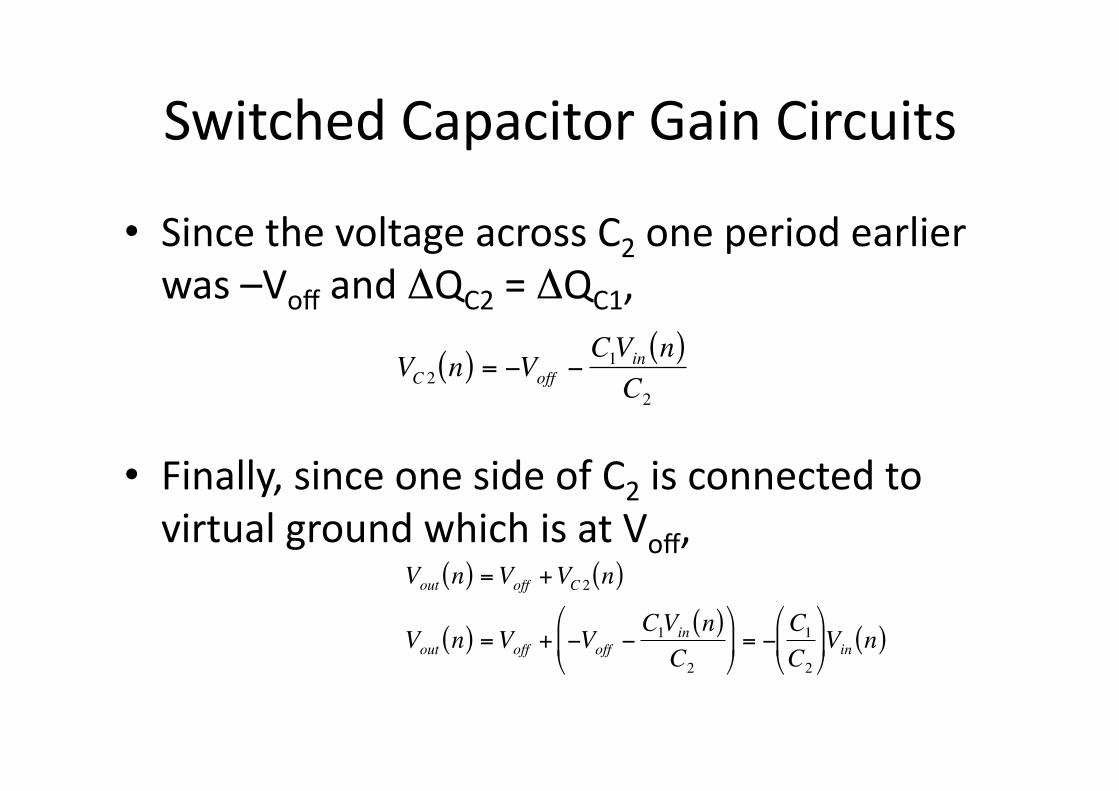
• Since the voltage across C2 one period earlier was –Voff and ΔQC2 = ΔQC1,
• Finally, since one side of C2 is connected to virtual ground which is at Voff,
€
VC 2 n( ) = −Voff −C1Vin n( )C2
€
Vout n( ) =Voff +VC 2 n( )
Vout n( ) =Voff + −Voff −C1Vin n( )C2
⎛
⎝ ⎜
⎞
⎠ ⎟ = −
C1C2
⎛
⎝ ⎜
⎞
⎠ ⎟ Vin n( )

Switched Capacitor Gain Circuits
• Note that offset cancella3on is also good for comba3ng 1/f noise.
• Also note that this structure requires a high slew rate from the OPAMP.
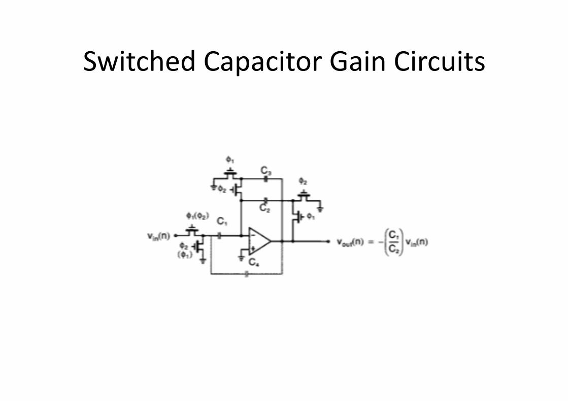
• A bejer structure is called the capaci3ve reset circuit and is as follows:
Switched Capacitor Gain Circuits

Switched Capacitor Gain Circuits
• The main idea here is the inclusion of C3 which charges to the output voltage during phase 1.
• During phase 2, it prevents the output from going to zero. The output remains near the previous output level.
• Also, during phase 2, the charges of C1 and C2 are equal and thus C3 does not effect the behavior of the circuit.