Embed Size (px)
Citation preview
SY87700AL
Low-Power, 3.3V, 32Mbps to 208Mbps AnyRate® Clock and Data Recovery
AnyRate is a registered trademark of Micrel, Inc. Micrel Inc. • 2180 Fortune Drive • San Jose, CA 95131 • USA • tel +1 (408) 944-0800 • fax + 1 (408) 474-1000 • http://www.micrel.com
August 2009
[email protected] or (408) 955-1690
General Description The SY87700AL is a complete clock recovery and data retiming integrated circuit for data rates from 32Mbps up to 208Mbps NRZ. The device is ideally suited for SONET/SDH/ATM applications and other high-speed data transmission systems. Clock recovery and data retiming is performed by synchronizing the on-chip VCO directly to the incoming data stream. The VCO center frequency is controlled by the reference clock frequency and the selected divide ratio. On-chip clock generation is performed through the use of a frequency multiplier PLL with a byte rate source as reference. The SY87700AL also includes a link fault detection circuit. Data sheets and support documentation can be found on Micrel’s web site at: www.micrel.com.
AnyRate® Features
• 3.3V power supply • SONET/SDH/ATM compatible • Clock and data recovery from 32Mbps up to
208Mbps NRZ data stream; clock generation from 32Mbps to 208Mbps
• Two on-chip PLLs: one for clock generation and another for clock recovery
• Selectable reference frequencies • Differential PECL high-speed serial I/O • Line receiver input: no external buffering needed • Link fault indication • 100K ECL-compatible I/O • Industrial temperature range (–40°C to +85°C) • Low power: fully compatible with Micrel’s SY87700V,
but with 30% less power • Available in 32-pin EPAD-TQFP and 28-pin EPAD
SOIC packages, (28-pin SOIC is available, but NOT recommended for new designs.)
Applications • SONET/SDH/ATM OC-1 and OC-3 • Fast Ethernet, SMPTE 259 • Proprietary architecture up to 208Mbps
Micrel, Inc. SY87700AL
August 2009 2 [email protected] or (408) 955-1690
Ordering Information(1) Part Number Package
Type Operating
Range Package Marking
Lead Finish
SY87700ALZG(2) Z28-1 Industrial SY87700ALZG with Pb-Free bar-line indicator
NiPdAu Pb-Free
SY87700ALHG(2) H32-1 Industrial SY87700ALHG with Pb-Free bar-line indicator
NiPdAu Pb-Free
Notes: 1. Contact factory for die availability. Dice are guaranteed at TA = 25°C, DC Electricals only. 2. Pb-Free package is recommended for new designs.
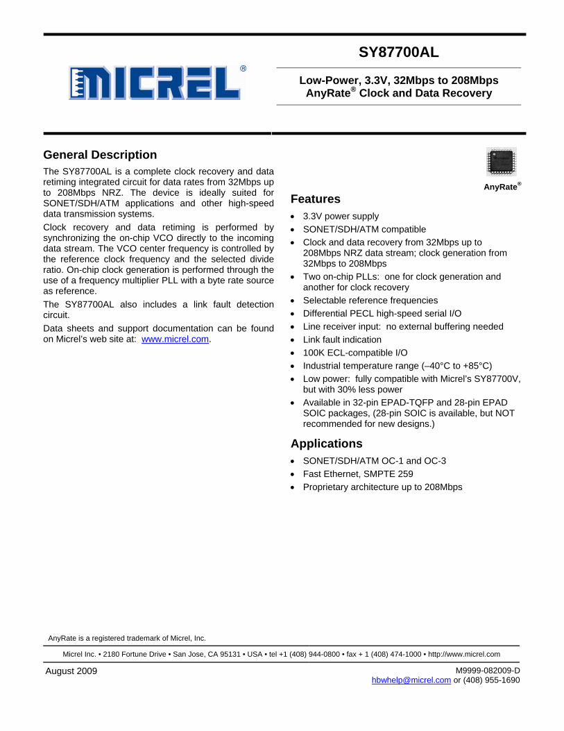
Pin Configuration
28-Pin SOIC (Z28-1)
32-Pin EPAD-TQFP (H32-1)
Micrel, Inc. SY87700AL
August 2009 3 [email protected] or (408) 955-1690
Pin Description Inputs
Pin Number (28-SOIC)
Pin Number (32-TQFP)
Pin Name Pin Name
4, 5
2, 3
RDINP, RDINN
Serial Data Input. Differential PECL: These built-in line receiver inputs are connected to the differential receive serial data stream. An internal receive PLL recovers the embedded clock (RCLK) and data (RDOUT) information. The incoming data rate can be within one of eight frequency ranges depending on the state of the FREQSEL pins. See “Frequency Selection” Table.
7 5 REFCLK Reference Clock. TTL Input: This input is used as the reference for the internal frequency synthesizer and the “training” frequency for the receiver PLL to keep it centered in the absence of data coming in on the RDIN inputs
27 26 CD Carrier Detect. PECL Input: This input controls the recovery function of the Receive PLL and can be driven by the carrier detect output of optical modules or from external transition detection circuitry. When this input is HIGH the input data stream (RDIN) is recovered normally by the Receive PLL. When this input is LOW the data on the inputs RDIN will be internally forced to a constant LOW, the data outputs RDOUT will remain LOW, the Link Fault Indicator output LFIN forced LOW and the clock recovery PLL forced to lock onto the clock frequency generated from REFCLK.
6 8 9
4 6 7
FREQSEL1 FREQSEL2 FREQSEL3
Frequency Select. TTL Inputs: These inputs select the output clock frequency range as shown in the “Frequency Selection” Table.
3 26
32 25
DIVSEL1 DIVSEL2
Divider Select. TTL Inputs: These inputs select the ratio between the output clock frequency (RCLK/TCLK) and the REFCLK input frequency as shown in the “Reference Frequency Selection” Table.
17 16 CLKSEL Clock Select. TTL Input: This input is used to select either the recovered clock of the receiver PLL (CLKSEL = HIGH) or the clock of the frequency synthesizer (CLKSEL = LOW) to the TCLK outputs.
Outputs 2 31 LFIN Link Fault Indicator. TTL Output: This output indicates the status of the input
data stream RDIN. Active HIGH signal is indicating when the internal clock recovery PLL has locked onto the incoming data stream. LFIN will go HIGH if CD is HIGH and RDIN is within the frequency range of the Receive PLL (1000ppm). LFIN is an asynchronous output.
25 24
24 23
RDOUTP RDOUTN
Receive Data Output. Differential PECL: These ECL 100k outputs represent the recovered data from the input data stream (RDIN). This recovered data is specified against the rising edge of RCLK.
22, 21 21, 20 RCLKP, RCLKN
Clock Output. Differential PECL: These ECL 100k outputs represent the recovered clock used to sample the recovered data (RDOUT).
19, 18 18, 17 TCLKP, TCLKN
Clock Output. Differential PECL: These ECL 100k outputs represent either the recovered clock (CLKSEL = HIGH) used to sample the recovered data (RDOUT) or the transmit clock of the frequency synthesizer (CLKSEL = LOW).
11, 12 9, 10 PLLSP, PLLSN
Clock Synthesis PLL Loop Filter: External loop filter pins for the clock synthesis PLL.
16, 15 15, 14 PLLRP, PLLRN
Clock Recovery PLL Loop Filter: External loop filter pins for the receiver PLL.
Micrel, Inc. SY87700AL
August 2009 4 [email protected] or (408) 955-1690
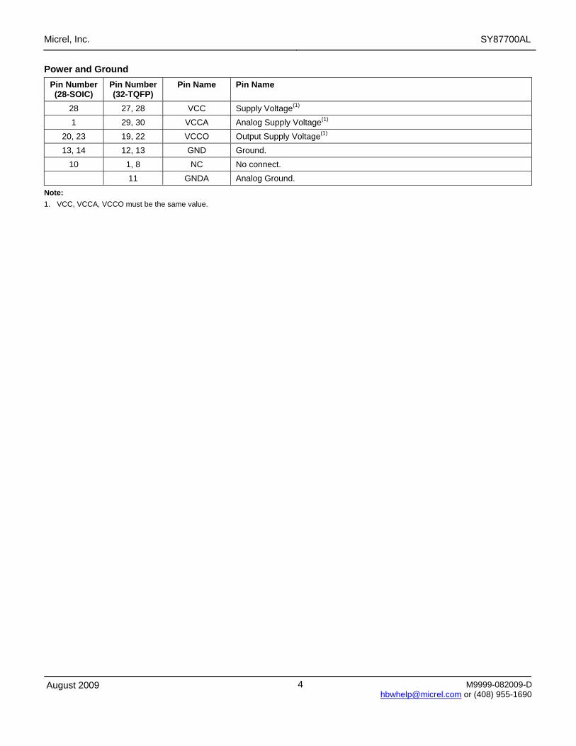
Power and Ground Pin Number (28-SOIC)
Pin Number (32-TQFP)
Pin Name Pin Name
28 27, 28 VCC Supply Voltage(1) 1 29, 30 VCCA Analog Supply Voltage(1)
20, 23 19, 22 VCCO Output Supply Voltage(1) 13, 14 12, 13 GND Ground.
10 1, 8 NC No connect. 11 GNDA Analog Ground.
Note: 1. VCC, VCCA, VCCO must be the same value.
Micrel, Inc. SY87700AL
August 2009 5 [email protected] or (408) 955-1690
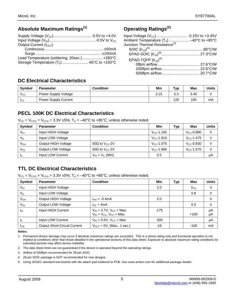
Absolute Maximum Ratings(1)
Supply Voltage (VCC) ................................... -0.5V to +4.0V Input Voltage (VIN) ........................................... -0.5V to VCC Output Current (IOUT) Continuous........................................................±50mA Surge ..............................................................±100mA Lead Temperature (soldering, 20sec.) ................... +260°C Storage Temperature (Ts) ........................-65°C to +150°C
Operating Ratings(2)
Input Voltage (VCC)............................. -3.15V to +3.45V Ambient Temperature (TA) ................... –40°C to +85°C Junction Thermal Resistance(3) SOIC (θJA)(4) ................................................. 80°C/W EPAD-SOIC (θJA)(5).................................... 27.3°C/W EPAD-TQFP (θJA)(5) 0lfpm airflow........................................ 27.6°C/W 200lfpm airflow.................................... 22.6°C/W 500lfpm airflow.................................... 20.7°C/W
DC Electrical Characteristics Symbol Parameter Condition Min Typ Max Units VCC Power Supply Voltage 3.15 3.3 3.45 V ICC Power Supply Current 120 160 mA
PECL 100K DC Electrical Characteristics VCC = VCCO = VCCA = 3.3V ±5%; TA = –40°C to +85°C, unless otherwise noted.
Symbol Parameter Condition Min Typ Max Units VIH Input HIGH Voltage VCC-1.165 VCC-0.880 V VIL Input LOW Voltage VCC-1.810 VCC-1.475 V VOH Output HIGH Voltage 50Ω to VCC-2V VCC-1.075 VCC-0.830 V VOL Output LOW Voltage 50Ω to VCC-2V VCC-1.860 VCC-1.570 V IIL Input LOW Current VIN = VIL (Min) 0.5 µA
TTL DC Electrical Characteristics VCC = VCCO = VCCA = 3.3V ±5%; TA = –40°C to +85°C, unless otherwise noted.
Symbol Parameter Condition Min Typ Max Units VIH Input HIGH Voltage 2.0 VCC V VIL Input LOW Voltage 0.8 V VOH Output HIGH Voltage IOH = -0.4mA 2.0 V VOL Output LOW Voltage IOL = 4mA 0.5 V IIH Input HIGH Current VIN = 2.7V, VCC = Max.
VIN = VCC, VCC = Max. -175
+100 µA µA
IIL Input LOW Current VIN = 0.5V, VCC = Max. -300 µA IOS Output Short-Circuit Current VOUT = 0V, (Max., 1 sec.) -15 -100 mA
Notes: 1. Permanent device damage may occur if absolute maximum ratings are exceeded. This is a stress rating only and functional operation is not
implied at conditions other than those detailed in the operational sections of this data sheet. Exposure to absolute maximum rating conditions for extended periods may affect device reliability.
2. The data sheet limits are not guaranteed if the device is operated beyond the operating ratings. 3. Airflow of 500lfpm recommended for 28-pin SOIC. 4. 28-pin SOIC package is NOT recommended for new designs. 5. Using JEDEC standard test boards with die attach pad soldered to PCB. See www.amkor.com for additional package details.
Micrel, Inc. SY87700AL
August 2009 6 [email protected] or (408) 955-1690
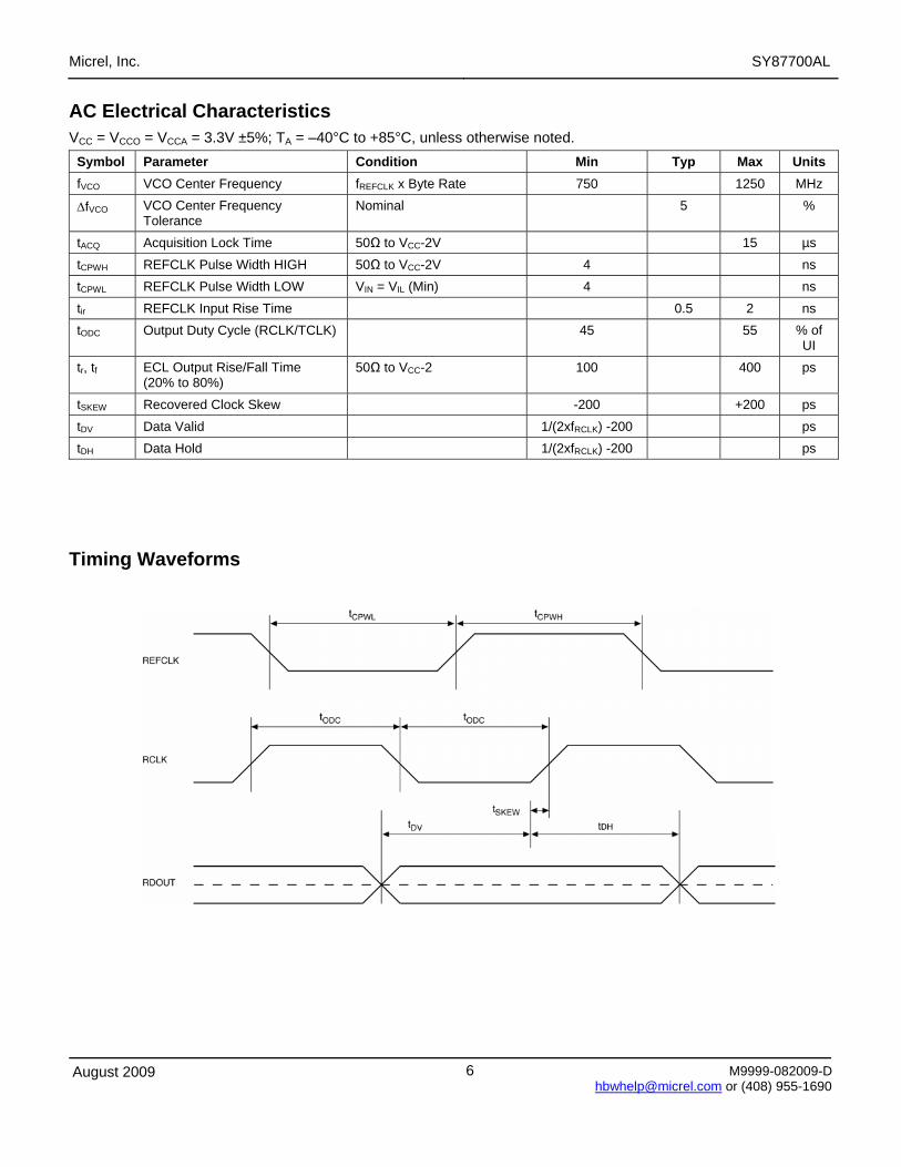
AC Electrical Characteristics VCC = VCCO = VCCA = 3.3V ±5%; TA = –40°C to +85°C, unless otherwise noted.
Symbol Parameter Condition Min Typ Max Units fVCO VCO Center Frequency fREFCLK x Byte Rate 750 1250 MHz
ΔfVCO VCO Center Frequency Tolerance
Nominal 5 %
tACQ Acquisition Lock Time 50Ω to VCC-2V 15 µs tCPWH REFCLK Pulse Width HIGH 50Ω to VCC-2V 4 ns tCPWL REFCLK Pulse Width LOW VIN = VIL (Min) 4 ns tir REFCLK Input Rise Time 0.5 2 ns tODC Output Duty Cycle (RCLK/TCLK) 45 55 % of
UI tr, tf ECL Output Rise/Fall Time
(20% to 80%) 50Ω to VCC-2 100 400 ps
tSKEW Recovered Clock Skew -200 +200 ps tDV Data Valid 1/(2xfRCLK) -200 ps tDH Data Hold 1/(2xfRCLK) -200 ps
Timing Waveforms
Micrel, Inc. SY87700AL
August 2009 7 [email protected] or (408) 955-1690
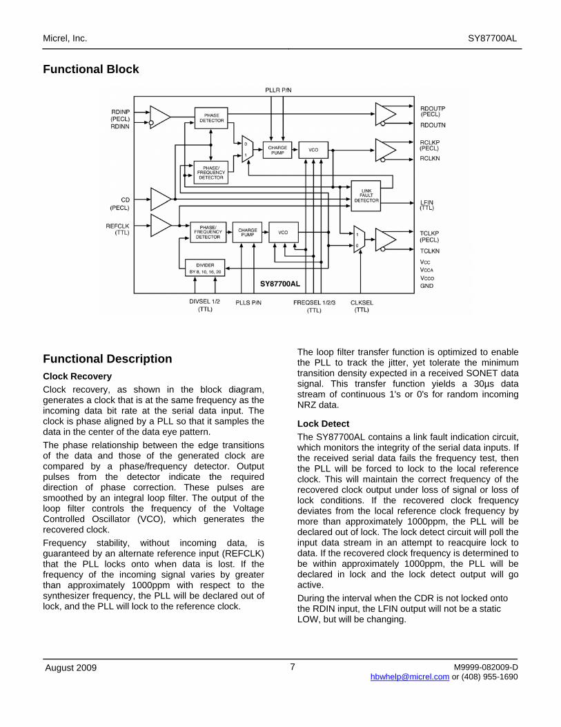
Functional Block
Functional Description Clock Recovery Clock recovery, as shown in the block diagram, generates a clock that is at the same frequency as the incoming data bit rate at the serial data input. The clock is phase aligned by a PLL so that it samples the data in the center of the data eye pattern. The phase relationship between the edge transitions of the data and those of the generated clock are compared by a phase/frequency detector. Output pulses from the detector indicate the required direction of phase correction. These pulses are smoothed by an integral loop filter. The output of the loop filter controls the frequency of the Voltage Controlled Oscillator (VCO), which generates the recovered clock. Frequency stability, without incoming data, is guaranteed by an alternate reference input (REFCLK) that the PLL locks onto when data is lost. If the frequency of the incoming signal varies by greater than approximately 1000ppm with respect to the synthesizer frequency, the PLL will be declared out of lock, and the PLL will lock to the reference clock.
The loop filter transfer function is optimized to enable the PLL to track the jitter, yet tolerate the minimum transition density expected in a received SONET data signal. This transfer function yields a 30µs data stream of continuous 1's or 0's for random incoming NRZ data.
Lock Detect The SY87700AL contains a link fault indication circuit, which monitors the integrity of the serial data inputs. If the received serial data fails the frequency test, then the PLL will be forced to lock to the local reference clock. This will maintain the correct frequency of the recovered clock output under loss of signal or loss of lock conditions. If the recovered clock frequency deviates from the local reference clock frequency by more than approximately 1000ppm, the PLL will be declared out of lock. The lock detect circuit will poll the input data stream in an attempt to reacquire lock to data. If the recovered clock frequency is determined to be within approximately 1000ppm, the PLL will be declared in lock and the lock detect output will go active. During the interval when the CDR is not locked onto the RDIN input, the LFIN output will not be a static LOW, but will be changing.
Micrel, Inc. SY87700AL
August 2009 8 [email protected] or (408) 955-1690
.
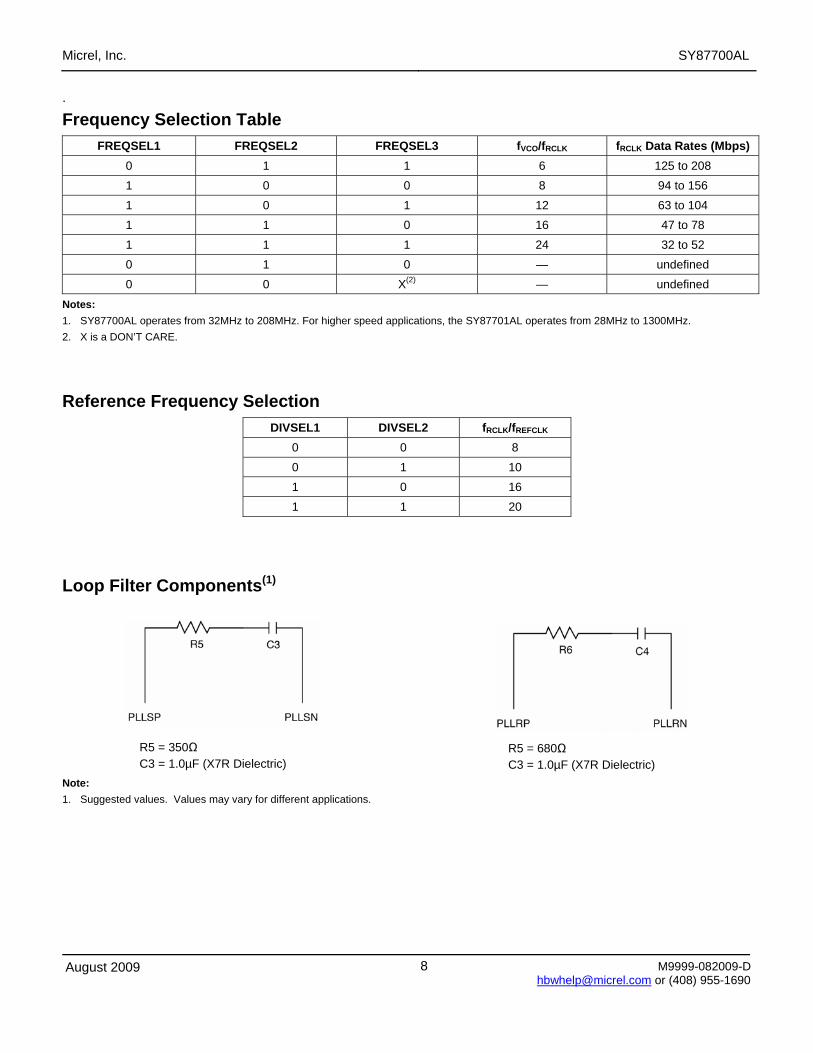
Frequency Selection Table FREQSEL1 FREQSEL2 FREQSEL3 fVCO/fRCLK fRCLK Data Rates (Mbps)
0 1 1 6 125 to 208 1 0 0 8 94 to 156 1 0 1 12 63 to 104 1 1 0 16 47 to 78 1 1 1 24 32 to 52 0 1 0 — undefined 0 0 X(2) — undefined
Notes: 1. SY87700AL operates from 32MHz to 208MHz. For higher speed applications, the SY87701AL operates from 28MHz to 1300MHz. 2. X is a DON’T CARE.
Reference Frequency Selection DIVSEL1 DIVSEL2 fRCLK/fREFCLK
0 0 8 0 1 10 1 0 16 1 1 20
Loop Filter Components(1)
R5 = 350Ω C3 = 1.0µF (X7R Dielectric)
R5 = 680Ω C3 = 1.0µF (X7R Dielectric)
Note: 1. Suggested values. Values may vary for different applications.
Micrel, Inc. SY87700AL
August 2009 9 [email protected] or (408) 955-1690
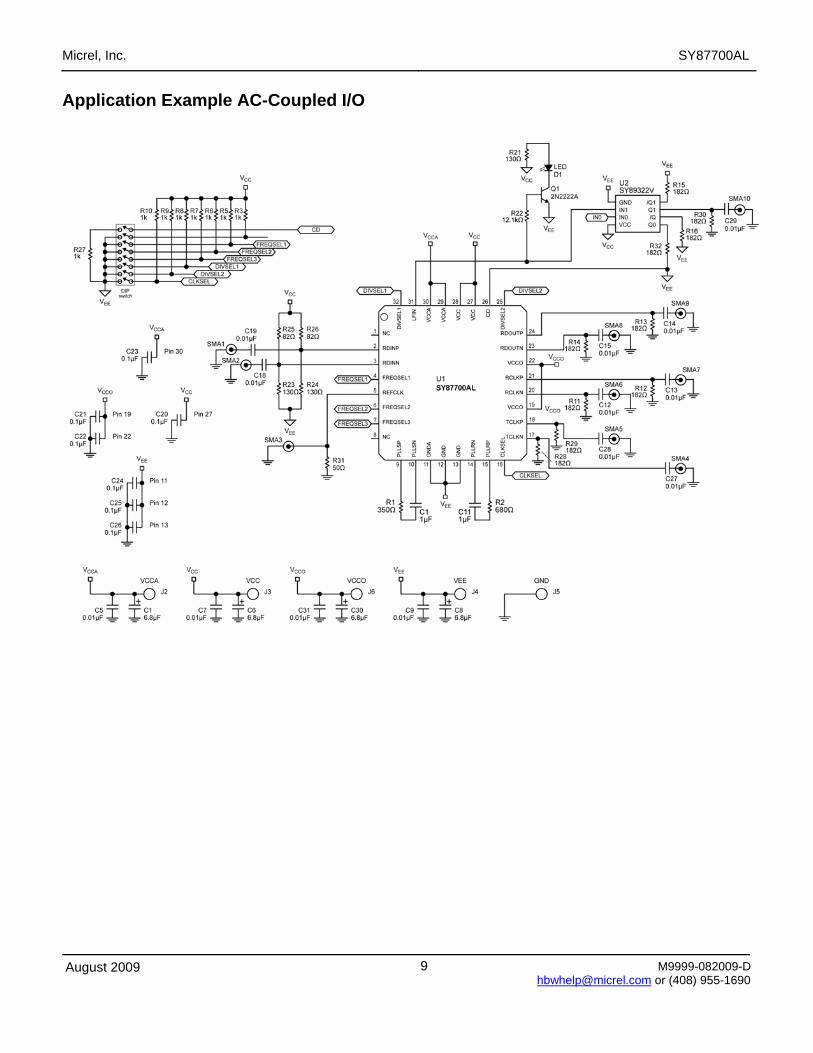
Application Example AC-Coupled I/O
Micrel, Inc. SY87700AL
August 2009 10 [email protected] or (408) 955-1690
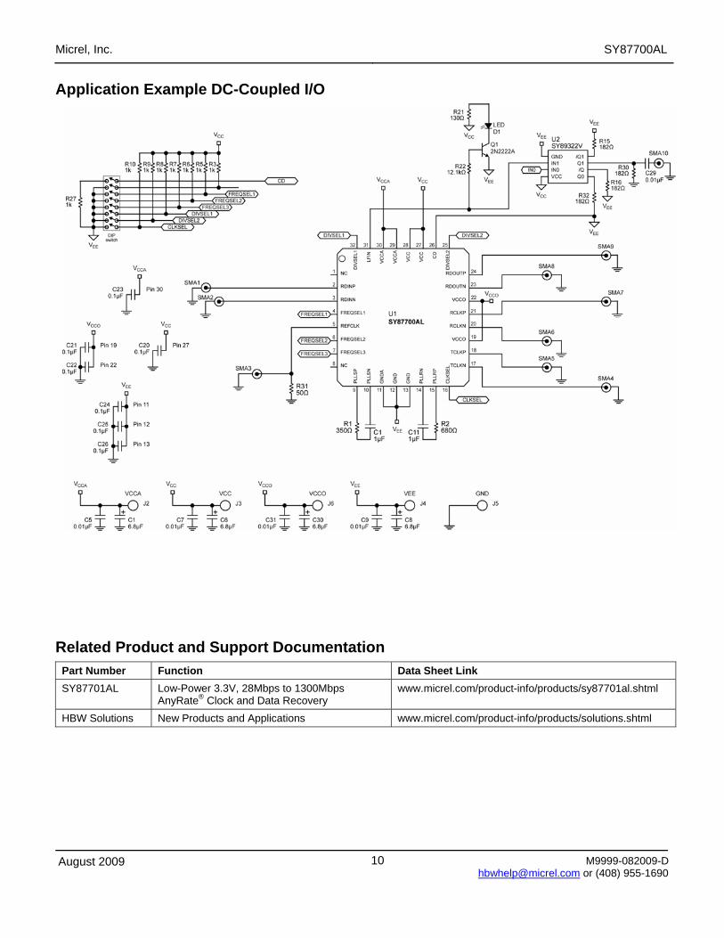
Application Example DC-Coupled I/O
Related Product and Support Documentation Part Number Function Data Sheet Link SY87701AL Low-Power 3.3V, 28Mbps to 1300Mbps
AnyRate® Clock and Data Recovery www.micrel.com/product-info/products/sy87701al.shtml
HBW Solutions New Products and Applications www.micrel.com/product-info/products/solutions.shtml
Micrel, Inc. SY87700AL
August 2009 11 [email protected] or (408) 955-1690
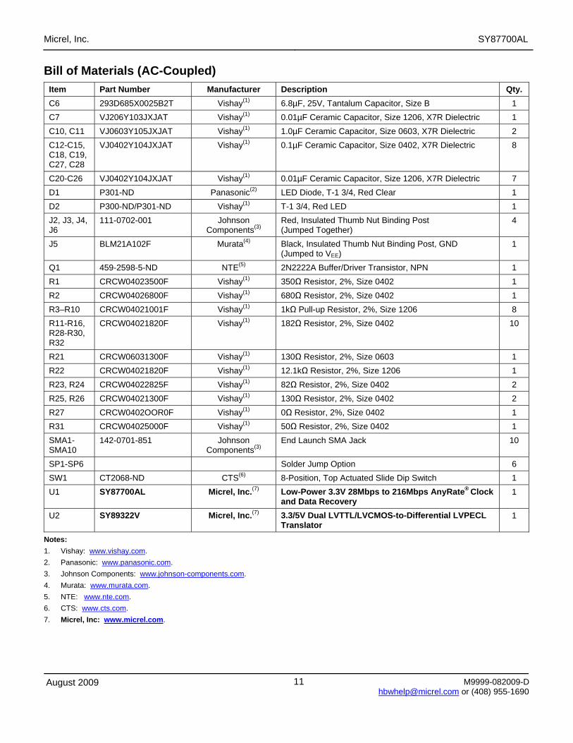
Bill of Materials (AC-Coupled) Item Part Number Manufacturer Description Qty. C6 293D685X0025B2T Vishay(1) 6.8µF, 25V, Tantalum Capacitor, Size B 1 C7 VJ206Y103JXJAT Vishay(1) 0.01µF Ceramic Capacitor, Size 1206, X7R Dielectric 1 C10, C11 VJ0603Y105JXJAT Vishay(1) 1.0µF Ceramic Capacitor, Size 0603, X7R Dielectric 2 C12-C15, C18, C19, C27, C28
VJ0402Y104JXJAT Vishay(1) 0.1µF Ceramic Capacitor, Size 0402, X7R Dielectric 8
C20-C26 VJ0402Y104JXJAT Vishay(1) 0.01µF Ceramic Capacitor, Size 1206, X7R Dielectric 7 D1 P301-ND Panasonic(2) LED Diode, T-1 3/4, Red Clear 1 D2 P300-ND/P301-ND Vishay(1) T-1 3/4, Red LED 1 J2, J3, J4, J6
111-0702-001 Johnson Components(3)
Red, Insulated Thumb Nut Binding Post (Jumped Together)
4
J5 BLM21A102F Murata(4) Black, Insulated Thumb Nut Binding Post, GND (Jumped to VEE)
1
Q1 459-2598-5-ND NTE(5) 2N2222A Buffer/Driver Transistor, NPN 1 R1 CRCW04023500F Vishay(1) 350Ω Resistor, 2%, Size 0402 1 R2 CRCW04026800F Vishay(1) 680Ω Resistor, 2%, Size 0402 1 R3–R10 CRCW04021001F Vishay(1) 1kΩ Pull-up Resistor, 2%, Size 1206 8 R11-R16, R28-R30, R32
CRCW04021820F Vishay(1) 182Ω Resistor, 2%, Size 0402 10
R21 CRCW06031300F Vishay(1) 130Ω Resistor, 2%, Size 0603 1 R22 CRCW04021820F Vishay(1) 12.1kΩ Resistor, 2%, Size 1206 1 R23, R24 CRCW04022825F Vishay(1) 82Ω Resistor, 2%, Size 0402 2 R25, R26 CRCW04021300F Vishay(1) 130Ω Resistor, 2%, Size 0402 2 R27 CRCW0402OOR0F Vishay(1) 0Ω Resistor, 2%, Size 0402 1 R31 CRCW04025000F Vishay(1) 50Ω Resistor, 2%, Size 0402 1 SMA1-SMA10
142-0701-851 Johnson Components(3)
End Launch SMA Jack 10
SP1-SP6 Solder Jump Option 6 SW1 CT2068-ND CTS(6) 8-Position, Top Actuated Slide Dip Switch 1 U1 SY87700AL Micrel, Inc.(7) Low-Power 3.3V 28Mbps to 216Mbps AnyRate® Clock
and Data Recovery 1
U2 SY89322V Micrel, Inc.(7) 3.3/5V Dual LVTTL/LVCMOS-to-Differential LVPECL Translator
1
Notes: 1. Vishay: www.vishay.com. 2. Panasonic: www.panasonic.com. 3. Johnson Components: www.johnson-components.com. 4. Murata: www.murata.com. 5. NTE: www.nte.com. 6. CTS: www.cts.com. 7. Micrel, Inc: www.micrel.com.
Micrel, Inc. SY87700AL
August 2009 12 [email protected] or (408) 955-1690
Bill of Materials (DC-Coupled) Item Part Number Manufacturer Description Qty. C6 293D685X0025B2T Vishay(1) 6.8µF, 25V, Tantalum Capacitor, Size B 1 C7 VJ206Y103JXJAT Vishay(1) 0.01µF Ceramic Capacitor, Size 1206, X7R Dielectric 1 C10, C11 VJ0603Y105JXJAT Vishay(1) 1.0µF Ceramic Capacitor, Size 0603, X7R Dielectric 2 C12-C15, C18, C19, C27, C28
VJ0402Y104JXJAT Vishay(1) 0.1µF Ceramic Capacitor, Size 0402, X7R Dielectric 8
C20-C26 VJ0402Y104JXJAT Vishay(1) 0.01µF Ceramic Capacitor, Size 1206, X7R Dielectric 7 D1 P301-ND Panasonic(2) LED Diode, T-1 3/4, Red Clear 1 D2 P300-ND/P301-ND Vishay(1) T-1 3/4, Red LED 1 J2, J3, J4, J6
111-0702-001 Johnson Components(3)
Red, Insulated Thumb Nut Binding Post (Jumped Together)
4
J5 BLM21A102F Johnson Components(3)
Black, Insulated Thumb Nut Binding Post, GND (Jumped to VEE)
1
Q1 459-2598-5-ND NTE(5) 2N2222A Buffer/Driver Transistor, NPN 1 R1 CRCW04023500F Vishay(1) 350Ω Resistor, 2%, Size 0402 1 R2 CRCW04026800F Vishay(1) 680Ω Resistor, 2%, Size 0402 1 R3–R10 CRCW04021001F Vishay(1) 1kΩ Pull-up Resistor, 2%, Size 1206 8 R15, R16, R30, R32
CRCW04021820F Vishay(1) 182Ω Resistor, 2%, Size 0402 10
R21 CRCW06031300F Vishay(1) 130Ω Resistor, 2%, Size 0603 1 R22 CRCW04021820F Vishay(1) 12.1kΩ Resistor, 2%, Size 1206 1 R23, R24 CRCW04022825F Vishay(1) 82Ω Resistor, 2%, Size 0402 2 R27 CRCW0402OOR0F Vishay(1) 0Ω Resistor, 2%, Size 0402 1 R31 CRCW04025000F Vishay(1) 50Ω Resistor, 2%, Size 0402 1 SMA1-SMA10
142-0701-851 Johnson Components(3)
End Launch SMA Jack 10
SP1-SP6 Solder Jump Option 6 SW1 CT2068-ND CTS(6) 8-Position, Top Actuated Slide Dip Switch 1 U1 SY87700AL Micrel, Inc.(7) Low-Power 3.3V 28Mbps to 216Mbps AnyRate® Clock
and Data Recovery 1
U2 SY89322V Micrel, Inc.(7) 3.3/5V Dual LVTTL/LVCMOS-to-Differential LVPECL Translator
1
Notes: 5. Vishay: www.vishay.com. 6. Panasonic: www.panasonic.com. 7. Johnson Components: www.johnson-components.com. 8. Murata: www.murata.com. 5. NTE: www.nte.com. 6. CTS: www.cts.com. 7. Micrel, Inc: www.micrel.com.
Micrel, Inc. SY87700AL
August 2009 13 [email protected] or (408) 955-1690
Appendix A Layout and General Suggestions 1. Establish controlled impedance stripline, microstrip, or
coplanar construction techniques. 2. Signal paths should have approximately the same width
as the device pads. 3. All differential paths are critical timing paths, where
skew should be matched to within ±10ps. 4. Signal trace impedance should not vary more than
±5%. If in doubt, perform TDR analysis of all high-speed signal traces.
5. Maintain compact filter networks as close to filter pins as possible. Provide ground plane relief under filter path to reduce stray capacitance. Be careful of crosstalk coupling into the filter network.
6. Maintain low jitter on the REFCLK input. Isolate the XTAL oscillator from power supply noise by adequately decoupling. Keep XTAL oscillator close to device, and minimize capacitive coupling from adjacent signals.
7. Higher speed operation may require use of fundamental-tone (third-overtone typically has more jitter) crystal-based oscillator for optimum performance. Evaluate and compare candidates by measuring TXCLK jitter.
8. All unused outputs must be terminated. To conserve power, unused PECL outputs can be terminated with a 1kΩ resistor to VEE.
Micrel, Inc. SY87700AL
August 2009 14 [email protected] or (408) 955-1690
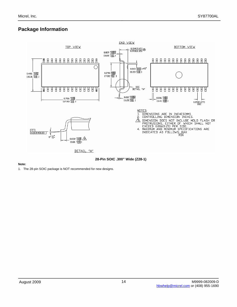
Package Information
28-Pin SOIC .300” Wide (Z28-1) Note: 1. The 28-pin SOIC package is NOT recommended for new designs.
Micrel, Inc. SY87700AL
August 2009 15 [email protected] or (408) 955-1690
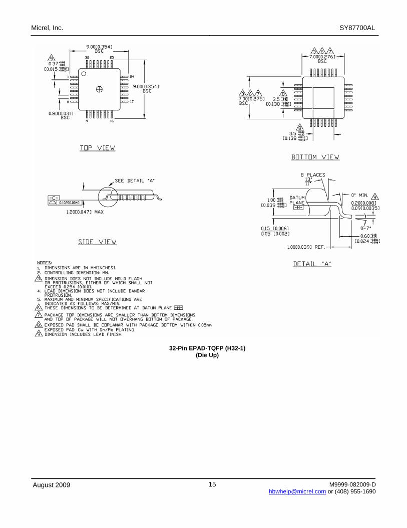
32-Pin EPAD-TQFP (H32-1) (Die Up)
Micrel, Inc. SY87700AL
August 2009 16 [email protected] or (408) 955-1690
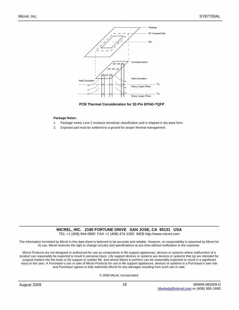
PCB Thermal Consideration for 32-Pin EPAD-TQFP
Package Notes: 1. Package meets Leve 2 moisture sensitivity classification and is shipped in dry-pack form. 2. Exposed pad must be soldered to a ground for proper thermal management.
MICREL, INC. 2180 FORTUNE DRIVE SAN JOSE, CA 95131 USA TEL +1 (408) 944-0800 FAX +1 (408) 474-1000 WEB http://www.micrel.com
The information furnished by Micrel in this data sheet is believed to be accurate and reliable. However, no responsibility is assumed by Micrel for
its use. Micrel reserves the right to change circuitry and specifications at any time without notification to the customer.
Micrel Products are not designed or authorized for use as components in life support appliances, devices or systems where malfunction of a product can reasonably be expected to result in personal injury. Life support devices or systems are devices or systems that (a) are intended for
surgical implant into the body or (b) support or sustain life, and whose failure to perform can be reasonably expected to result in a significant injury to the user. A Purchaser’s use or sale of Micrel Products for use in life support appliances, devices or systems is a Purchaser’s own risk
and Purchaser agrees to fully indemnify Micrel for any damages resulting from such use or sale.
© 2006 Micrel, Incorporated.