Embed Size (px)
Citation preview
SATHYABAMA UNIVERSITY(Established under section 3 of UGC Act, 1956)
Jeppiaar Nagar, Rajiv Gandhi Salai, Chennai - 119.
SYLLABUS
MASTER OF ENGINEERING PROGRAMMEIN
APPLIED ELECTRONICS(4 SEMESTERS)
REGULATIONS 2010
SATHYABAMA UNIVERSITYREGULATIONS – 2010
Effective from the academic year 2010-2011 and applicable to the students admitted to the Master of Engineering/ Technology / Architecture /Science (Four Semesters)
1. Structure of Programme
1.1 Every Programme will have a curriculum with syllabi consisting theory and practical such as:
(i) General core courses like Mathematics
(ii) Core course of Engineering / Technology/Architecture / Science
(iii) Elective course for specialization in related fields
(iv) Workshop practice, Computer Practice, laboratory Work, Industrial Training, SeminarPresentation, Project Work, Educational Tours, Camps etc.
1.2 Each semester curriculum shall normally have a blend of lecture course not exceeding 7 and practicalcourse not exceeding 4.
1.3 The medium of instruction, examinations and project report will be English.
2. Duration of the Programme
A student is normally expected to complete the M.E/M.Tech./M.Arch/M.Sc Programme in 4 semesters but inany case not more than 8 consecutive semesters from the time of commencement of the course. TheHead of the Department shall ensure that every teacher imparts instruction as per the number of hours specifiedin the syllabus and that the teacher teaches the full content of the specified syllabus for the course beingtaught.
3. Requirements for Completion of a Semester
A candidate who has fulfilled the following conditions shall be deemed to have satisfied the requirement forcompletion of a semester.
3.1 He/She secures not less than 90% of overall attendance in that semester.
3.2 Candidates who do not have the requisite attendance for the semester will not be permitted towrite the University Exams.
4. Examinations
The examinations shall normally be conducted between October and December during the odd semesters andbetween March and May in the even semesters. The maximum marks for each theory and practical course(including the project work and Viva Voce examination in the Fourth Semester) shall be 100 with the followingbreakup.
(i) Theory Courses
Internal Assessment : 20 Marks
University Exams : 80 Marks
(ii) Practical courses
Internal Assessment : - -
University Exams : 100 Marks
SATHYABAMA UNIVERSITY FACULTY OF ELECTRONICS ENGINEERING
M.E (APPLIED ELECTRONICS) i REGULATIONS 2010
5. Passing requirements:
(i) A candidate who secures not less than 50% of total marks prescribed for the course (For all coursesincluding Theory, Practicals and Project work) with a minimum of 40 marks out of 80 in the UniversityTheory Examinations, shall be declared to have passed in the Examination.
(ii) If a candidate fails to secure a Pass in a particular course, it is mandatory that he/she shall reappearfor the examination in that course during the next semester when examination is conducted in thatcourse. However the Internal Assessment marks obtained by the candidate in the first attempt shallbe retained and considered valid for all subsequent attempts.
6. Eligibility for the Award of Degree
A student shall be declared to be eligible for the award of the M.E/M.Tech./M.Arch./M.Sc degree provided thestudent has successfully completed the course requirements and has passed all the prescribed examinations inall the 4 semesters within the maximum period specified in clause 2.
7. Award of Credits and Grades:
All assessments of a course will be done on absolute marks basis. However, for the purpose of reporting theperformance of a candidate, Letter Grades will be awarded as per the range of total marks (out of 100) obtainedby the candidate as given below:
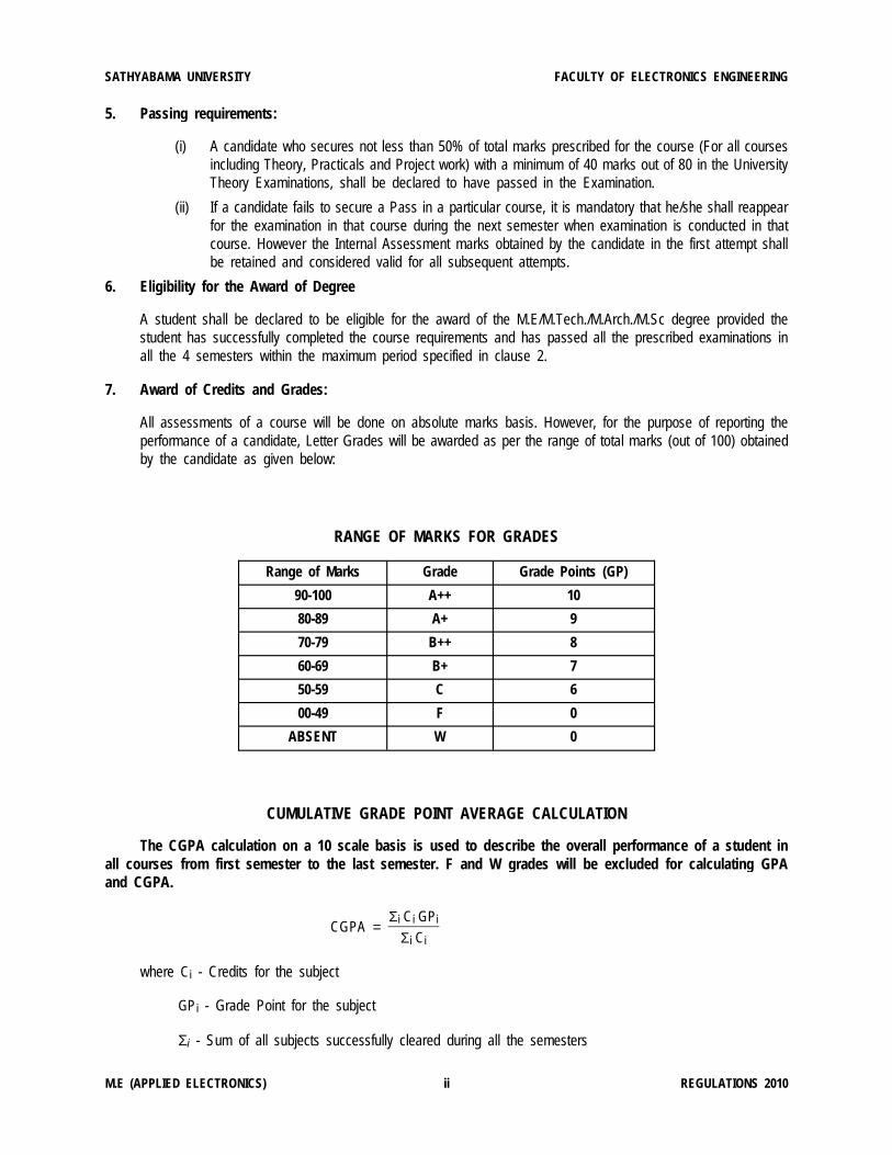
RANGE OF MARKS FOR GRADES
Range of Marks Grade Grade Points (GP)
90-100 A++ 10
80-89 A+ 9
70-79 B++ 8
60-69 B+ 7
50-59 C 6
00-49 F 0
ABSENT W 0
CUMULATIVE GRADE POINT AVERAGE CALCULATION
The CGPA calculation on a 10 scale basis is used to describe the overall performance of a student inall courses from first semester to the last semester. F and W grades will be excluded for calculating GPAand CGPA.
CGPA = Σi Ci GPi
Σi Ci
where Ci - Credits for the subject
GPi - Grade Point for the subject
Σi - Sum of all subjects successfully cleared during all the semesters
SATHYABAMA UNIVERSITY FACULTY OF ELECTRONICS ENGINEERING
M.E (APPLIED ELECTRONICS) ii REGULATIONS 2010
8. Classification of the Degree Awarded
1 A candidate who qualifies for the award of the Degree having passed the examination in all thecourses of all the semesters in his/her first appearance within a maximum period of 4 consecutivesemesters after commencement of study securing a CGPA not less than 9.0 shall be declared tohave passed the examination in First Class – Exemplary.
2. A candidate who qualifies for the award of the Degree having passed the examination in all thecourses of all the semesters in his/her first appearance within a maximum period of 4 consecutivesemesters after commencement of study, securing a CGPA not less than 7.5 shall be declared tohave passed the examination in First Class with Distinction.
3. A candidate who qualifies for the award of the Degree having passed the examination in all thecourses of all the semesters in his/her first appearance within a maximum period of 4 consecutivesemesters after commencement of study securing a CGPA not less than 6.0 shall be declared tohave passed the examination in First Class.
4 All other candidates who qualify for the award of the Degree having passed the examination in allthe courses of all the 4 semesters within a maximum period of 8 consecutive semesters after his/hercommencement of study securing a CGPA not less than 5.0 shall be declared to have passedthe examination in Second Class.
5 A candidate who is absent in semester examination in a course/project work after having registeredfor the same, shall be considered to have appeared in that examination for the purpose ofclassification of degree. For all the above mentioned classification of Degree, the break of studyduring the programme, will be counted for the purpose of classification of degree.
6 A candidate can apply for revaluation of his/her semester examination answer paper in a theorycourse, within 1 week from the declaration of results, on payment of a prescribed fee along withprescribed application to the Controller of Examinations through the Head of Department. TheController of Examination will arrange for the revaluation and the result will be intimated to thecandidate concerned through the Head of the Department. Revaluation is not permitted for practicalcourses and for project work.
Final Degree is awarded based on the following :
CGPA ≥ 9.0 - First Class - Exemplary
CGPA ≥ 7.50 < 9.0 - First Class with Distinction
CGPA ≥ 6.00 < 7.50 - First Class
CGPA ≥ 5.00 < 6.00 - Second Class
Minimum CGPA requirements for award of Degree is 5.0 CGPA.
9. Discipline
Every student is required to observe disciplined and decorous behaviour both inside and outside the Universityand not to indulge in any activity which will tend to bring down the prestige of the University. If a studentindulges in malpractice in any of the University theory / practical examination, he/she shall be liable for punitiveaction as prescribed by the University from time to time.
10. Revision of Regulations and Curriculum
The University may revise, amend or change the regulations, scheme of examinations and syllabi from time totime, if found necessary.
SATHYABAMA UNIVERSITY FACULTY OF ELECTRONICS ENGINEERING
M.E (APPLIED ELECTRONICS) iii REGULATIONS 2010
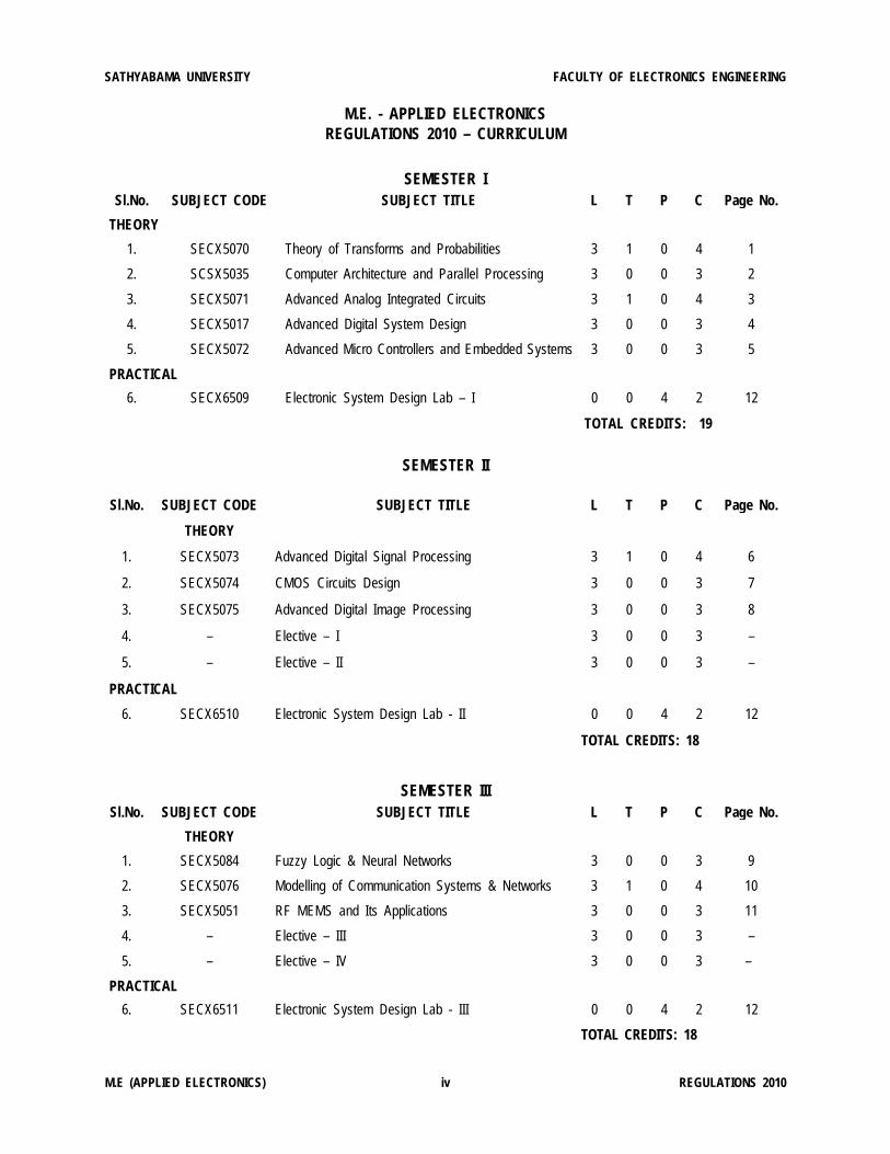
M.E. - APPLIED ELECTRONICSREGULATIONS 2010 – CURRICULUM
SEMESTER ISl.No. SUBJECT CODE SUBJECT TITLE L T P C Page No.
THEORY
1. SECX5070 Theory of Transforms and Probabilities 3 1 0 4 1
2. SCSX5035 Computer Architecture and Parallel Processing 3 0 0 3 2
3. SECX5071 Advanced Analog Integrated Circuits 3 1 0 4 3
4. SECX5017 Advanced Digital System Design 3 0 0 3 4
5. SECX5072 Advanced Micro Controllers and Embedded Systems 3 0 0 3 5
PRACTICAL
6. SECX6509 Electronic System Design Lab – I 0 0 4 2 12
TOTAL CREDITS: 19
SEMESTER II
Sl.No. SUBJECT CODE SUBJECT TITLE L T P C Page No.
THEORY
1. SECX5073 Advanced Digital Signal Processing 3 1 0 4 6
2. SECX5074 CMOS Circuits Design 3 0 0 3 7
3. SECX5075 Advanced Digital Image Processing 3 0 0 3 8
4. – Elective – I 3 0 0 3 –
5. – Elective – II 3 0 0 3 –
PRACTICAL
6. SECX6510 Electronic System Design Lab - II 0 0 4 2 12
TOTAL CREDITS: 18
SEMESTER IIISl.No. SUBJECT CODE SUBJECT TITLE L T P C Page No.
THEORY
1. SECX5084 Fuzzy Logic & Neural Networks 3 0 0 3 9
2. SECX5076 Modelling of Communication Systems & Networks 3 1 0 4 10
3. SECX5051 RF MEMS and Its Applications 3 0 0 3 11
4. – Elective – III 3 0 0 3 –
5. – Elective – IV 3 0 0 3 –
PRACTICAL
6. SECX6511 Electronic System Design Lab - III 0 0 4 2 12
TOTAL CREDITS: 18
SATHYABAMA UNIVERSITY FACULTY OF ELECTRONICS ENGINEERING
M.E (APPLIED ELECTRONICS) iv REGULATIONS 2010
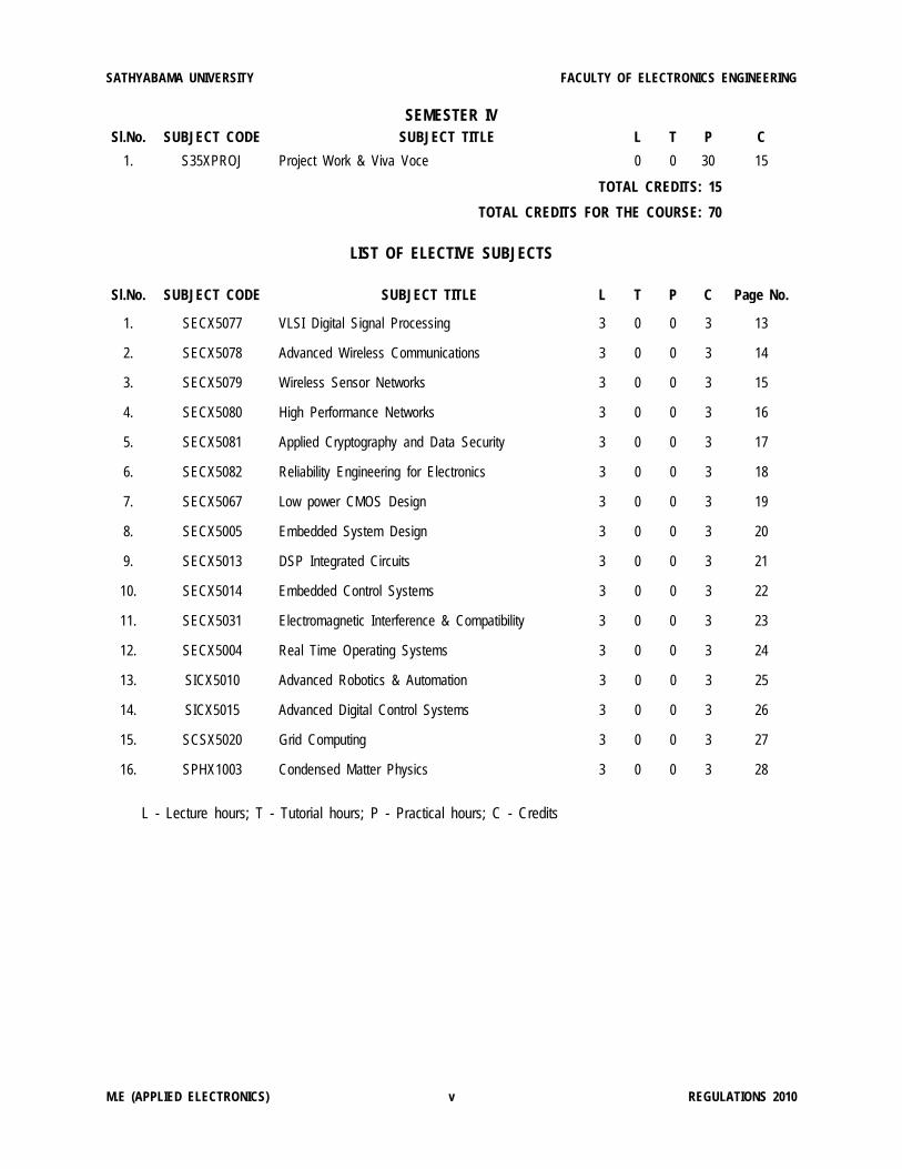
SEMESTER IVSl.No. SUBJECT CODE SUBJECT TITLE L T P C
1. S35XPROJ Project Work & Viva Voce 0 0 30 15
TOTAL CREDITS: 15
TOTAL CREDITS FOR THE COURSE: 70
LIST OF ELECTIVE SUBJECTS
Sl.No. SUBJECT CODE SUBJECT TITLE L T P C Page No.
1. SECX5077 VLSI Digital Signal Processing 3 0 0 3 13
2. SECX5078 Advanced Wireless Communications 3 0 0 3 14
3. SECX5079 Wireless Sensor Networks 3 0 0 3 15
4. SECX5080 High Performance Networks 3 0 0 3 16
5. SECX5081 Applied Cryptography and Data Security 3 0 0 3 17
6. SECX5082 Reliability Engineering for Electronics 3 0 0 3 18
7. SECX5067 Low power CMOS Design 3 0 0 3 19
8. SECX5005 Embedded System Design 3 0 0 3 20
9. SECX5013 DSP Integrated Circuits 3 0 0 3 21
10. SECX5014 Embedded Control Systems 3 0 0 3 22
11. SECX5031 Electromagnetic Interference & Compatibility 3 0 0 3 23
12. SECX5004 Real Time Operating Systems 3 0 0 3 24
13. SICX5010 Advanced Robotics & Automation 3 0 0 3 25
14. SICX5015 Advanced Digital Control Systems 3 0 0 3 26
15. SCSX5020 Grid Computing 3 0 0 3 27
16. SPHX1003 Condensed Matter Physics 3 0 0 3 28
L - Lecture hours; T - Tutorial hours; P - Practical hours; C - Credits
SATHYABAMA UNIVERSITY FACULTY OF ELECTRONICS ENGINEERING
M.E (APPLIED ELECTRONICS) v REGULATIONS 2010
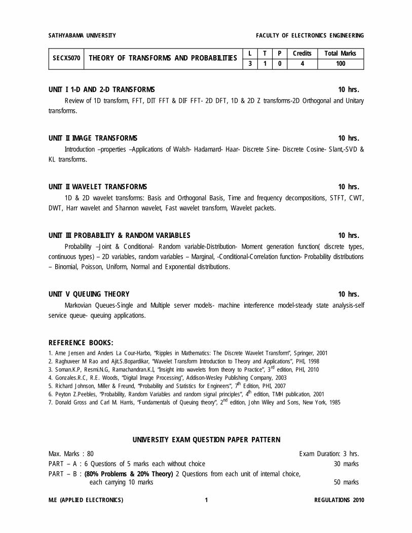
SECX5070 THEORY OF TRANSFORMS AND PROBABILITIESL T P Credits Total Marks
3 1 0 4 100
UNIT I 1-D AND 2-D TRANSFORMS 10 hrs.Review of 1D transform, FFT, DIT FFT & DIF FFT- 2D DFT, 1D & 2D Z transforms-2D Orthogonal and Unitary
transforms.
UNIT II IMAGE TRANSFORMS 10 hrs.Introduction –properties –Applications of Walsh- Hadamard- Haar- Discrete Sine- Discrete Cosine- Slant,-SVD &
KL transforms.
UNIT II WAVELET TRANSFORMS 10 hrs.1D & 2D wavelet transforms: Basis and Orthogonal Basis, Time and frequency decompositions, STFT, CWT,
DWT, Harr wavelet and Shannon wavelet, Fast wavelet transform, Wavelet packets.
UNIT III PROBABILITY & RANDOM VARIABLES 10 hrs.Probability –Joint & Conditional- Random variable-Distribution- Moment generation function( discrete types,
continuous types) – 2D variables, random variables – Marginal, -Conditional-Correlation function- Probability distributions– Binomial, Poisson, Uniform, Normal and Exponential distributions.
UNIT V QUEUING THEORY 10 hrs.Markovian Queues-Single and Multiple server models- machine interference model-steady state analysis-self
service queue- queuing applications.
REFERENCE BOOKS:1. Arne Jensen and Anders La Cour-Harbo, “Ripples in Mathematics: The Discrete Wavelet Transform”, Springer, 20012. Raghuveer M Rao and Ajit.S.Bopardikar, “Wavelet Transform Introduction to Theory and Applications”, PHI, 19983. Soman.K.P, Resmi.N.G, Ramachandran.K.I, “Insight into wavelets from theory to Practice”, 3 rd edition, PHI, 20104. Gonzales.R.C, R.E. Woods, “Digital Image Processing”, Addison-Wesley Publishing Company, 20035. Richard Johnson, Miller & Freund, “Probability and Statistics for Engineers”, 7th Edition, PHI, 20076. Peyton Z.Peebles, “Probability, Random Variables and random signal principles”, 4th edition, TMH publication, 20017. Donald Gross and Carl M. Harris, “Fundamentals of Queuing theory”, 2nd edition, John Wiley and Sons, New York, 1985
UNIVERSITY EXAM QUESTION PAPER PATTERN
Max. Marks : 80 Exam Duration: 3 hrs.PART – A : 6 Questions of 5 marks each without choice 30 marksPART – B : (80% Problems & 20% Theory) 2 Questions from each unit of internal choice, each carrying 10 marks 50 marks
SATHYABAMA UNIVERSITY FACULTY OF ELECTRONICS ENGINEERING
M.E (APPLIED ELECTRONICS) 1 REGULATIONS 2010
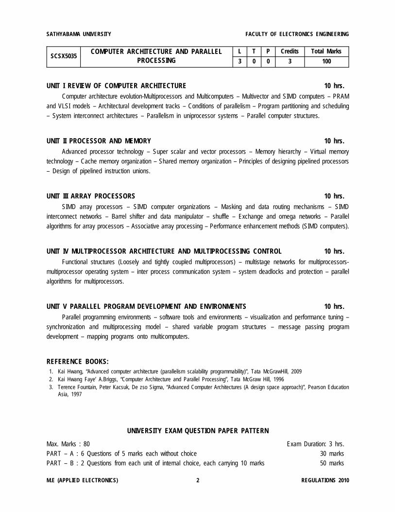
SCSX5035COMPUTER ARCHITECTURE AND PARALLEL
PROCESSINGL T P Credits Total Marks
3 0 0 3 100
UNIT I REVIEW OF COMPUTER ARCHITECTURE 10 hrs.Computer architecture evolution-Multiprocessors and Multicomputers – Multivector and SIMD computers – PRAM
and VLSI models – Architectural development tracks – Conditions of parallelism – Program partitioning and scheduling– System interconnect architectures – Parallelism in uniprocessor systems – Parallel computer structures.
UNIT II PROCESSOR AND MEMORY 10 hrs.Advanced processor technology – Super scalar and vector processors – Memory hierarchy – Virtual memory
technology – Cache memory organization – Shared memory organization – Principles of designing pipelined processors– Design of pipelined instruction unions.
UNIT III ARRAY PROCESSORS 10 hrs.SIMD array processors – SIMD computer organizations – Masking and data routing mechanisms – SIMD
interconnect networks – Barrel shifter and data manipulator – shuffle – Exchange and omega networks – Parallelalgorithms for array processors – Associative array processing – Performance enhancement methods (SIMD computers).
UNIT IV MULTIPROCESSOR ARCHITECTURE AND MULTIPROCESSING CONTROL 10 hrs.Functional structures (Loosely and tightly coupled multiprocessors) – multistage networks for multiprocessors-
multiprocessor operating system – inter process communication system – system deadlocks and protection – parallelalgorithms for multiprocessors.
UNIT V PARALLEL PROGRAM DEVELOPMENT AND ENVIRONMENTS 10 hrs.Parallel programming environments – software tools and environments – visualization and performance tuning –
synchronization and multiprocessing model – shared variable program structures – message passing programdevelopment – mapping programs onto multicomputers.
REFERENCE BOOKS: 1. Kai Hwang, “Advanced computer architecture (parallelism scalability programmability)”, Tata McGrawHill, 2009 2. Kai Hwang Faye’ A.Briggs, “Computer Architecture and Parallel Processing”, Tata McGraw Hill, 1996 3. Terence Fountain, Peter Kacsuk, De zso Sigma, “Advanced Computer Architectures (A design space approach)”, Pearson Education
Asia, 1997
UNIVERSITY EXAM QUESTION PAPER PATTERN
Max. Marks : 80 Exam Duration: 3 hrs.PART – A : 6 Questions of 5 marks each without choice 30 marksPART – B : 2 Questions from each unit of internal choice, each carrying 10 marks 50 marks
SATHYABAMA UNIVERSITY FACULTY OF ELECTRONICS ENGINEERING
M.E (APPLIED ELECTRONICS) 2 REGULATIONS 2010
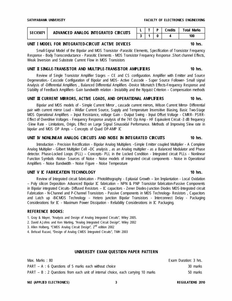
SECX5071 ADVANCED ANALOG INTEGRATED CIRCUITSL T P Credits Total Marks
3 1 0 4 100
UNIT I MODEL FOR INTEGRATED-CIRCUIT ACTIVE DEVICES 10 hrs.
Small-Signal Model of the Bipolar and MOS Transistor -Parasitic Elements, Specification of Transistor FrequencyResponse - Body Transconductance - Parasitic Elements - MOS Transistor Frequency Response .Short channel Effects,Weak Inversion and Substrate Current Flow in MOS Transistors
UNIT II SINGLE-TRANSISTOR AND MULTIPLE-TRANSISTOR AMPLIFIERS 10 hrs.
Review of Single Transistor Amplifier Stages – CE and CS configuration. Amplifier with Emitter and SourceDegeneration.- Cascode Configuration of Bipolar and MOS- Active Cascode - Super Source Follower- Small signalAnalysis of -Differential Amplifiers , Balanced Differential Amplifiers -Device Mismatch Effects-Frequency Response andStability of Feedback Amplifiers- Gain bandwidth relation - Instability and the Nyquist Criterion – Compensation methods
UNIT III CURRENT MIRRORS, ACTIVE LOADS, AND OPERATIONAL AMPLIFIERS 10 hrs.
Bipolar and MOS models of - Simple Current Mirror , cascade current mirrors, Wilson Current Mirror- Differentialpair with current mirror Load - Widlar Current Source, Supply and Temperature Insensitive Biasing, Basic Two-StageMOS Operational Amplifiers – Input Resistance, voltage Gain - Output Swing - Input Offset Voltage - CMRR- PSRR-Effect of Overdrive Voltages - Frequency Response analysis of the 741 Op Amp - HF Equivalent Circuit -3 dB frequency-Slew Rate - Limitations, Origin, Effect on Large Signal Sinusoidal Performance. Methods of Improving Slew rate inbipolar and MOS OP Amps – Concepts of Quad OP-AMP IC
UNIT IV NONLINEAR ANALOG CIRCUITS AND NOISE IN INTEGRATED CIRCUITS 10 hrs.
Introduction - Precision Rectification - Bipolar Analog Multipliers –Simple Emitter coupled Multiplier - A CompleteAnalog Multiplier - Gilbert Multiplier Cell –DC analysis , as an Analog multiplier - as a Balanced Modulator and Phasedetector. Phase-Locked Loops (PLL) – Concepts- PLL in the Locked Condition - Integrated circuit PLLs - NonlinearFunction Symbols -Noise- Sources of Noise - Noise models of integrated circuit components - Noise in OperationalAmplifiers - Noise Bandwidth - Noise Figure - Noise Temperature
UNIT V IC FABRICATION TECHNOLOGY 10 hrs.
Review of Integrated circuit fabrication - Photolithography - Epitaxial Growth – Ion Implantation - Local Oxidation– Poly silicon Deposition- Advanced Bipolar IC fabrication – NPN & PNP Transistor fabrication-Passive Componentsin Bipolar integrated Circuits- Diffused Resistors – IC capacitors - Zener Diodes-Junction Diodes MOS-Integrated circuitFabrication - N-Channel and P-Channel Transistors - Passive Components in MOS Technology- Resistors , Capacitorsand Latch up -BiCMOS Technology – Hetero junction Bipolar Transistors - Interconnect Delay - PackagingConsiderations for IC - Maximum Power Dissipation - Reliability Considerations in IC Packaging.
REFERENCE BOOKS:1. Gray & Mayer, “Analysis and Design of Analog Integrated Circuits”, Wiley 2005.2. David A.Johns and Ken Marting, “Analog Integrated Circuit Design”, Wiley 20023. Allen Holberg, “CMOS Analog Circuit Design”, 2nd edition 20024. Behzad Razavi, “Design of Analog CMOS Integrated Circuits”, TMH 2003
UNIVERSITY EXAM QUESTION PAPER PATTERN
Max. Marks : 80 Exam Duration: 3 hrs.
PART – A : 6 Questions of 5 marks each without choice 30 marks
PART – B : 2 Questions from each unit of internal choice, each carrying 10 marks 50 marks
SATHYABAMA UNIVERSITY FACULTY OF ELECTRONICS ENGINEERING
M.E (APPLIED ELECTRONICS) 3 REGULATIONS 2010
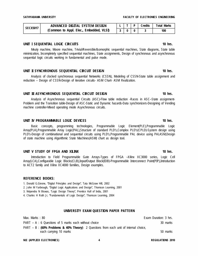
SECX5017ADVANCED DIGITAL SYSTEM DESIGN
(Common to Appl. Elec., Embedded, VLSI)L T P Credits Total Marks
3 0 0 3 100
UNIT I SEQUENTIAL LOGIC CIRCUITS 10 hrs.
Mealy machine, Moore machine, Trivial/Reversible/Isomorphic sequential machines, State diagrams, State tableminimization, Incompletely specified sequential machines, State assignments, Design of synchronous and asynchronoussequential logic circuits working in fundamental and pulse mode.
UNIT II SYNCHRONOUS SEQUENTIAL CIRCUIT DESIGN 10 hrs.
Analysis of clocked synchronous sequential Networks (CSSN), Modeling of CSSN-State table assignment andreduction – Design of CSSN-Design of iterative circuits- ASM Chart- ASM Realization.
UNIT III ASYNCHRONOUS SEQUENTIAL CIRCUIT DESIGN 10 hrs.
Analysis of Asynchronous sequential Circuits (ASC)-Flow table reduction -Races in ASC--State assignment-Problem and the Transition table-Design of ASC-Static and Dynamic hazards-Data synchronizers-Designing of Vendingmachine controller-Mixed operating mode Asynchronous circuits.
UNIT IV PROGRAMMABLE LOGIC DEVICES 10 hrs.
Basic concepts, programming technologies, Programmable Logic Element(PLE),Programmable LogicArray(PLA),Programmable Array Logic(PAL),Structure of standard PLD’s,Complex PLD’s(CPLD)-System design usingPLD’s-Design of combinational and sequential circuits using PLD’s,Programmable PAL device using PALASM,Designof state machine using Algorithmic State Machines(ASM) chart as design tool.
UNIT V STUDY OF FPGA AND XILINX 10 hrs.
Introduction to Field Programmable Gate Arrays-Types of FPGA –Xilinx XC3000 series, Logic CellArray(LCA),Configurable Logic Blocks(CLB),Input/Output Block(IOB)-Programmable Interconnect Point(PIP),Introductionto ACT2 family and Xilinx XC4000 families, Design examples.
REFERENCE BOOKS:1. Donald G.Givone, “Digital Principles and Design”, Tata McGraw Hill, 20022. John M Yarbrough, “Digital Logic Applications and Design”, Thomson Learning, 20013. Nripendra N Biswas, “Logic Design Theory”, Prentice Hall of India, 20014. Charles H Roth Jr, “Fundamentals of Logic Design”, Thomson Learning, 2004
UNIVERSITY EXAM QUESTION PAPER PATTERN
Max. Marks : 80 Exam Duration: 3 hrs.
PART – A : 6 Questions of 5 marks each without choice 30 marks
PART – B : (60% Problems & 40% Theory) 2 Questions from each unit of internal choice, each carrying 10 marks 50 marks
SATHYABAMA UNIVERSITY FACULTY OF ELECTRONICS ENGINEERING
M.E (APPLIED ELECTRONICS) 4 REGULATIONS 2010
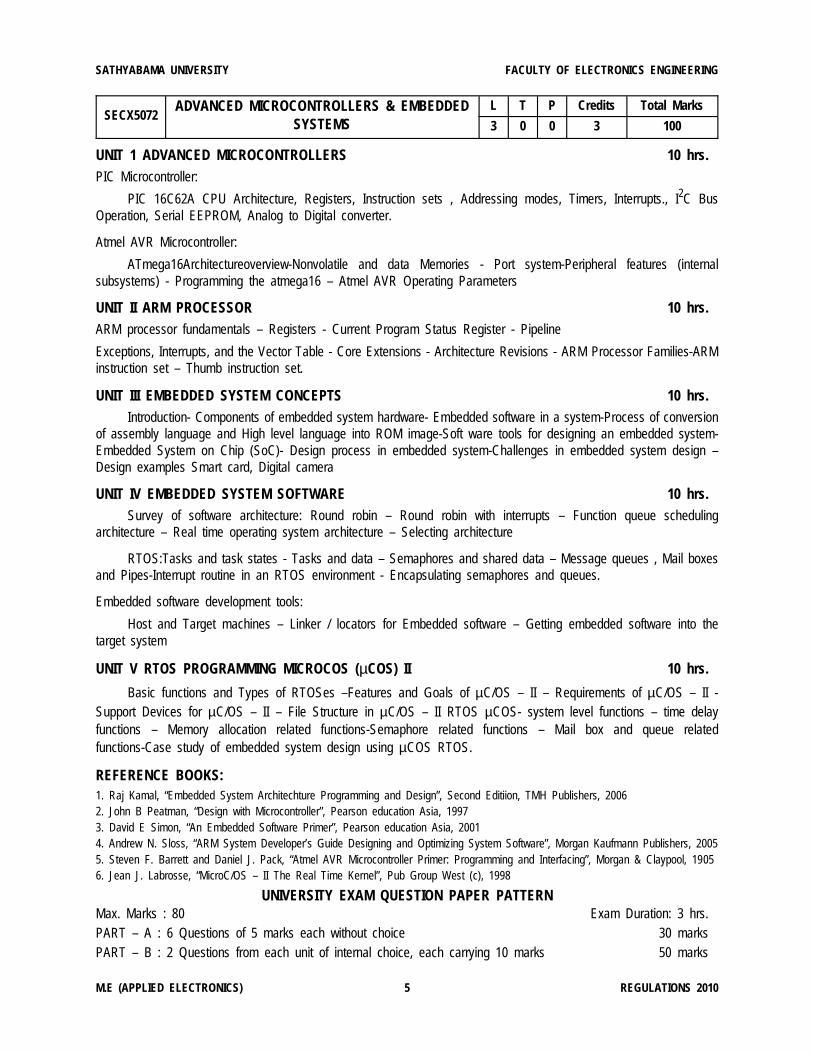
SECX5072ADVANCED MICROCONTROLLERS & EMBEDDED
SYSTEMSL T P Credits Total Marks
3 0 0 3 100
UNIT 1 ADVANCED MICROCONTROLLERS 10 hrs.PIC Microcontroller:
PIC 16C62A CPU Architecture, Registers, Instruction sets , Addressing modes, Timers, Interrupts., I2C BusOperation, Serial EEPROM, Analog to Digital converter.
Atmel AVR Microcontroller:
ATmega16Architectureoverview-Nonvolatile and data Memories - Port system-Peripheral features (internalsubsystems) - Programming the atmega16 – Atmel AVR Operating Parameters
UNIT II ARM PROCESSOR 10 hrs.ARM processor fundamentals – Registers - Current Program Status Register - Pipeline
Exceptions, Interrupts, and the Vector Table - Core Extensions - Architecture Revisions - ARM Processor Families-ARMinstruction set – Thumb instruction set.
UNIT III EMBEDDED SYSTEM CONCEPTS 10 hrs.Introduction- Components of embedded system hardware- Embedded software in a system-Process of conversion
of assembly language and High level language into ROM image-Soft ware tools for designing an embedded system-Embedded System on Chip (SoC)- Design process in embedded system-Challenges in embedded system design –Design examples Smart card, Digital camera
UNIT IV EMBEDDED SYSTEM SOFTWARE 10 hrs.Survey of software architecture: Round robin – Round robin with interrupts – Function queue scheduling
architecture – Real time operating system architecture – Selecting architecture
RTOS:Tasks and task states - Tasks and data – Semaphores and shared data – Message queues , Mail boxesand Pipes-Interrupt routine in an RTOS environment - Encapsulating semaphores and queues.
Embedded software development tools:
Host and Target machines – Linker / locators for Embedded software – Getting embedded software into thetarget system
UNIT V RTOS PROGRAMMING MICROCOS (µCOS) II 10 hrs.
Basic functions and Types of RTOSes –Features and Goals of µC/OS – II – Requirements of µC/OS – II -Support Devices for µC/OS – II – File Structure in µC/OS – II RTOS µCOS- system level functions – time delayfunctions – Memory allocation related functions-Semaphore related functions – Mail box and queue relatedfunctions-Case study of embedded system design using µCOS RTOS.
REFERENCE BOOKS:1. Raj Kamal, “Embedded System Architechture Programming and Design”, Second Editiion, TMH Publishers, 20062. John B Peatman, “Design with Microcontroller”, Pearson education Asia, 19973. David E Simon, “An Embedded Software Primer”, Pearson education Asia, 20014. Andrew N. Sloss, “ARM System Developer’s Guide Designing and Optimizing System Software”, Morgan Kaufmann Publishers, 20055. Steven F. Barrett and Daniel J. Pack, “Atmel AVR Microcontroller Primer: Programming and Interfacing”, Morgan & Claypool, 19056. Jean J. Labrosse, “MicroC/OS – II The Real Time Kernel”, Pub Group West (c), 1998
UNIVERSITY EXAM QUESTION PAPER PATTERNMax. Marks : 80 Exam Duration: 3 hrs.PART – A : 6 Questions of 5 marks each without choice 30 marksPART – B : 2 Questions from each unit of internal choice, each carrying 10 marks 50 marks
SATHYABAMA UNIVERSITY FACULTY OF ELECTRONICS ENGINEERING
M.E (APPLIED ELECTRONICS) 5 REGULATIONS 2010
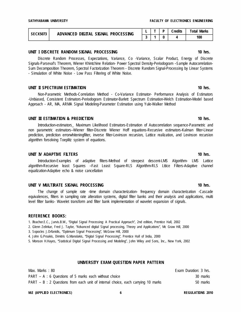
SECX5073 ADVANCED DIGITAL SIGNAL PROCESSINGL T P Credits Total Marks
3 1 0 4 100
UNIT I DISCRETE RANDOM SIGNAL PROCESSING 10 hrs.Discrete Random Processes, Expectations, Variance, Co -Variance, Scalar Product, Energy of Discrete
Signals-Parseval’s Theorem, Wiener Khintchine Relation- Power Spectral Density-Periodogram –Sample Autocorrelation-Sum Decomposition Theorem, Spectral Factorization Theorem - Discrete Random Signal-Processing by Linear Systems- Simulation of White Noise - Low Pass Filtering of White Noise.
UNIT II SPECTRUM ESTIMATION 10 hrs.Non-Parametric Methods-Correlation Method - Co-Variance Estimator- Performance Analysis of Estimators
-Unbiased, Consistent Estimators-Periodogram Estimator-Barlett Spectrum Estimation-Welch Estimation-Model basedApproach - AR, MA, ARMA Signal Modeling-Parameter Estimation using Yule-Walker Method
UNIT III ESTIMATION & PREDICTION 10 hrs.Introduction-estimators_ Maximum Likelihood Estimators-Estimation of Autocorrelation sequence-Parametric and
non parametric estimators--Wiener filter-Discrete Wiener Hoff equations-Recursive estimators-Kalman filter-Linearprediction, prediction errorwhiteningfilter, inverse filter-Levinson recursion, Lattice realization, and Levinson recursionalgorithm forsolving Toeplitz system of equations.
UNIT IV ADAPTIVE FILTERS 10 hrs.Introduction-Examples of adaptive filters-Method of steepest descent-LMS Algorithm- LMS Lattice
algorithm-Recursive least Squares –Fast Least Square-RLS Algorithm-RLS Lttice Filters-Adaptive channelequalization-Adaptive echo & noise cancellation
UNIT V MULTIRATE SIGNAL PROCESSING 10 hrs.The change of sample rate -time domain characterization- frequency domain characterization -Cascade
equivalences, filters in sampling rate alteration systems, digital filter banks and their analysis and applications, multilevel filter banks- Wavelet transform and filter bank implementation of wavelet expansion of signals.
REFERENCE BOOKS:1. Ifeachor.E.C., Jarvis.B.W., “Digital Signal Processing: A Practical Approach”, 2nd edition, Prentice Hall, 20022. Glenn Zelinkar, Fred J. Taylor, “Advanced digital Signal processing, Theory and Applications”, Mc Graw Hill, 20003. Sopocles J.Orfanidis, “Optimum Signal Processing”, McGraw Hill, 20004. John G.Proakis, Dimitris G.Manolakis, “Digital Signal Processing”, Prentice Hall of India, 20005. Monson H.Hayes, “Statistical Digital Signal Processing and Modeling”, John Wiley and Sons, Inc., New York, 2002
UNIVERSITY EXAM QUESTION PAPER PATTERN
Max. Marks : 80 Exam Duration: 3 hrs.PART – A : 6 Questions of 5 marks each without choice 30 marksPART – B : 2 Questions from each unit of internal choice, each carrying 10 marks 50 marks
SATHYABAMA UNIVERSITY FACULTY OF ELECTRONICS ENGINEERING
M.E (APPLIED ELECTRONICS) 6 REGULATIONS 2010
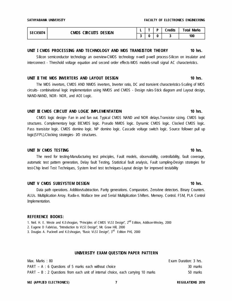
SECX5074 CMOS CIRCUITS DESIGNL T P Credits Total Marks
3 0 0 3 100
UNIT I CMOS PROCESSING AND TECHNOLOGY AND MOS TRANSISTOR THEORY 10 hrs.
Silicon semiconductor technology an overview-CMOS technology n-well p-well process-Silicon on insulator andinterconnect - Threshold voltage equation and second order effects-MOS models-small signal AC characteristics.
UNIT II THE MOS INVERTERS AND LAYOUT DESIGN 10 hrs.The MOS invertors, CMOS AND NMOS inverters, Inverter ratio, DC and transient characteristics-Scaling of MOS
circuits- combinational logic implementation using NMOS and CMOS - Design rules-Stick diagram and Layout design,NAND-NAND, NOR- NOR, and AOI Logic.
UNIT III CMOS CIRCUIT AND LOGIC IMPLEMENTATION 10 hrs.CMOS logic design- Fan in and fan out. Typical CMOS NAND and NOR delays.Transistor sizing. CMOS logic
structures. Complementary logic BICMOS logic. Pseudo NMOS logic. Dynamic CMOS logic. Clocked CMOS logic.Pass transistor logic. CMOS domino logic. NP domino logic. Cascade voltage switch logic. Source follower pull uplogic(SFPL).Clocking strategies- I/O structures.
UNIT IV CMOS TESTING 10 hrs.
The need for testing-Manufacturing test principles, Fault models, observability, controllability, fault coverage,automatic test pattern generation, Delay fault Testing, Statistical fault analysis, Fault sampling-Design strategies fortest-Chip level Test Techniques, System level test techniques-Layout design for improved testability
UNIT V CMOS SUBSYSTEM DESIGN 10 hrs.Data path operations. Addition/subtraction. Parity generations. Comparators. Zero/one detectors. Binary Counters.
ALUs. Multiplication Array. Radix-n. Wallace tree and Serial Multiplication Shifters. Memory. Control. FSM, PLA ControlImplementation.
REFERENCE BOOKS:1. Neil. H. E. Weste and K.Eshragian, “Principles of CMOS VLSI Design”, 2nd Edition, Addison-Wesley, 20002. Eugene D Fabricius, “Introduction to VLSI Design”, Mc Graw Hill, 20003. Douglas A. Pucknell and K.Eshragian, “Basic VLSI Design”, 3rd Edition PHI, 2000
UNIVERSITY EXAM QUESTION PAPER PATTERN
Max. Marks : 80 Exam Duration: 3 hrs.PART – A : 6 Questions of 5 marks each without choice 30 marksPART – B : 2 Questions from each unit of internal choice, each carrying 10 marks 50 marks
SATHYABAMA UNIVERSITY FACULTY OF ELECTRONICS ENGINEERING
M.E (APPLIED ELECTRONICS) 7 REGULATIONS 2010
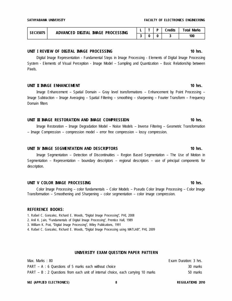
SECX5075 ADVANCED DIGITAL IMAGE PROCESSINGL T P Credits Total Marks
3 0 0 3 100
UNIT I REVIEW OF DIGITAL IMAGE PROCESSING 10 hrs.
Digital Image Representation - Fundamental Steps in Image Processing - Elements of Digital Image ProcessingSystem - Elements of Visual Perception - Image Model – Sampling and Quantization – Basic Relationship betweenPixels.
UNIT II IMAGE ENHANCEMENT 10 hrs.
Image Enhancement – Spatial Domain – Gray level transformations – Enhancement by Point Processing –Image Subtraction – Image Averaging – Spatial Filtering – smoothing – sharpening – Fourier Transform – FrequencyDomain filters
UNIT III IMAGE RESTORATION AND IMAGE COMPRESSION 10 hrs.
Image Restoration – Image Degradation Model – Noise Models – Inverse Filtering – Geometric Transformation– Image Compression – compression model – error free compression – lossy compression.
UNIT IV IMAGE SEGMENTATION AND DESCRIPTORS 10 hrs.
Image Segmentation – Detection of Discontinuities – Region Based Segmentation – The Use of Motion inSegmentation – Representation – boundary descriptors – regional descriptors – use of principal components fordescription.
UNIT V COLOR IMAGE PROCESSING 10 hrs.
Color Image Processing – color fundamentals – Color Models – Pseudo Color Image Processing – Color ImageTransformation – Smoothening and Sharpening – color segmentation – color image compression.
REFERENCE BOOKS:1. Rafael C. Gonzalez, Richard E. Woods, “Digital Image Processing”, PHI, 20082. Anil K. Jain, “Fundamentals of Digital Image Processing”, Prentice Hall, 19893. William K. Prat, “Digital Image Processing”, Wiley Publications, 19914. Rafael C. Gonzalez, Richard E. Woods, “Digital Image Processing using MATLAB”, PHI, 2009
UNIVERSITY EXAM QUESTION PAPER PATTERN
Max. Marks : 80 Exam Duration: 3 hrs.
PART – A : 6 Questions of 5 marks each without choice 30 marks
PART – B : 2 Questions from each unit of internal choice, each carrying 10 marks 50 marks
SATHYABAMA UNIVERSITY FACULTY OF ELECTRONICS ENGINEERING
M.E (APPLIED ELECTRONICS) 8 REGULATIONS 2010
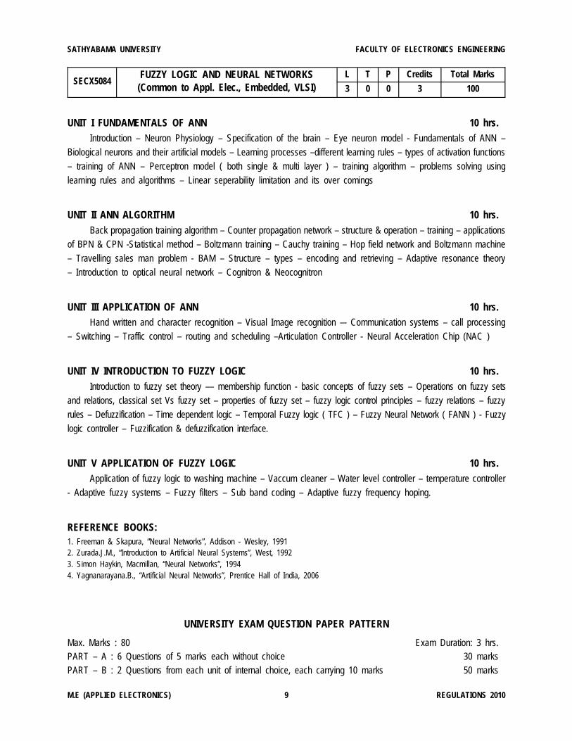
SECX5084FUZZY LOGIC AND NEURAL NETWORKS
(Common to Appl. Elec., Embedded, VLSI)L T P Credits Total Marks
3 0 0 3 100
UNIT I FUNDAMENTALS OF ANN 10 hrs.Introduction – Neuron Physiology – Specification of the brain – Eye neuron model - Fundamentals of ANN –
Biological neurons and their artificial models – Learning processes –different learning rules – types of activation functions– training of ANN – Perceptron model ( both single & multi layer ) – training algorithm – problems solving usinglearning rules and algorithms – Linear seperability limitation and its over comings
UNIT II ANN ALGORITHM 10 hrs.Back propagation training algorithm – Counter propagation network – structure & operation – training – applications
of BPN & CPN -Statistical method – Boltzmann training – Cauchy training – Hop field network and Boltzmann machine– Travelling sales man problem - BAM – Structure – types – encoding and retrieving – Adaptive resonance theory– Introduction to optical neural network – Cognitron & Neocognitron
UNIT III APPLICATION OF ANN 10 hrs.Hand written and character recognition – Visual Image recognition –- Communication systems – call processing
– Switching – Traffic control – routing and scheduling –Articulation Controller - Neural Acceleration Chip (NAC )
UNIT IV INTRODUCTION TO FUZZY LOGIC 10 hrs.Introduction to fuzzy set theory –– membership function - basic concepts of fuzzy sets – Operations on fuzzy sets
and relations, classical set Vs fuzzy set – properties of fuzzy set – fuzzy logic control principles – fuzzy relations – fuzzyrules – Defuzzification – Time dependent logic – Temporal Fuzzy logic ( TFC ) – Fuzzy Neural Network ( FANN ) - Fuzzylogic controller – Fuzzification & defuzzification interface.
UNIT V APPLICATION OF FUZZY LOGIC 10 hrs.Application of fuzzy logic to washing machine – Vaccum cleaner – Water level controller – temperature controller
- Adaptive fuzzy systems – Fuzzy filters – Sub band coding – Adaptive fuzzy frequency hoping.
REFERENCE BOOKS:1. Freeman & Skapura, “Neural Networks”, Addison - Wesley, 19912. Zurada.J.M., “Introduction to Artificial Neural Systems”, West, 19923. Simon Haykin, Macmillan, “Neural Networks”, 19944. Yagnanarayana.B., “Artificial Neural Networks”, Prentice Hall of India, 2006
UNIVERSITY EXAM QUESTION PAPER PATTERN
Max. Marks : 80 Exam Duration: 3 hrs.PART – A : 6 Questions of 5 marks each without choice 30 marksPART – B : 2 Questions from each unit of internal choice, each carrying 10 marks 50 marks
SATHYABAMA UNIVERSITY FACULTY OF ELECTRONICS ENGINEERING
M.E (APPLIED ELECTRONICS) 9 REGULATIONS 2010
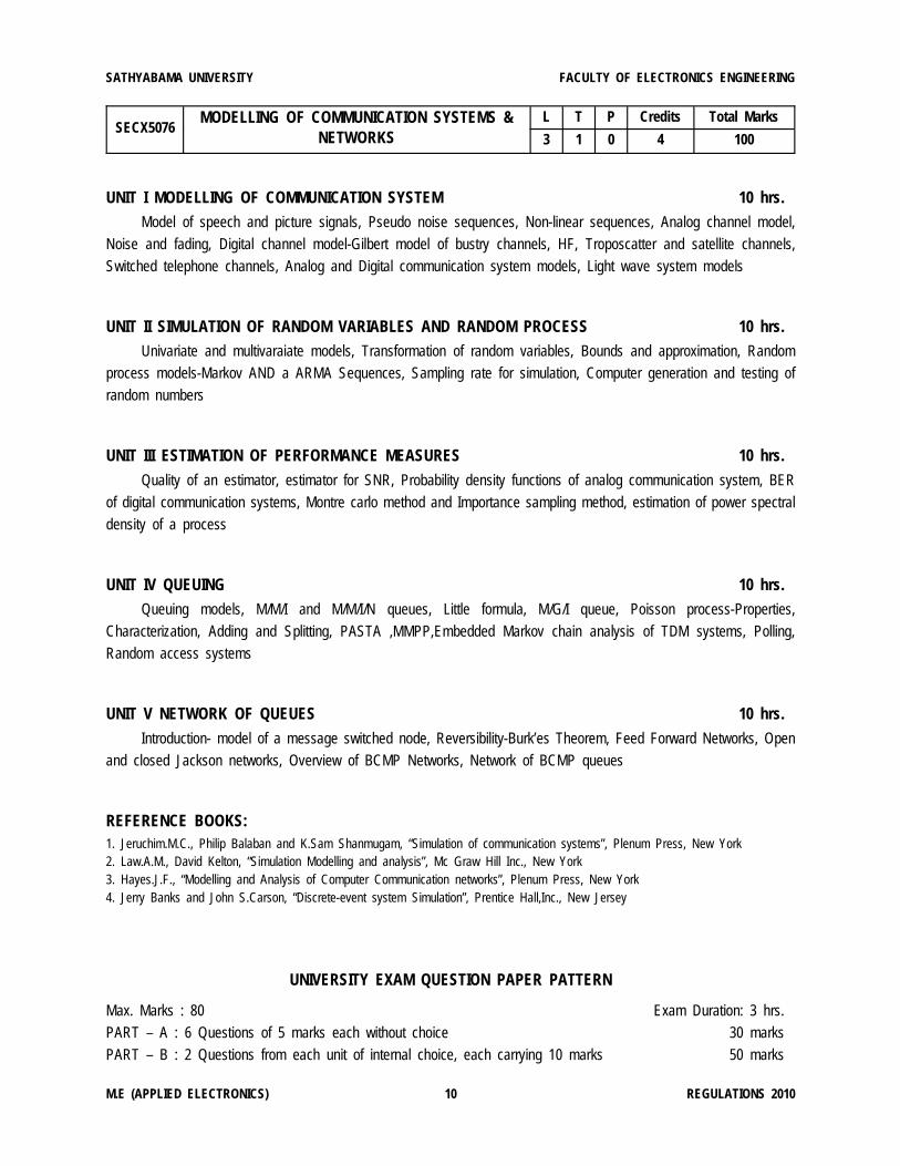
SECX5076MODELLING OF COMMUNICATION SYSTEMS &
NETWORKSL T P Credits Total Marks
3 1 0 4 100
UNIT I MODELLING OF COMMUNICATION SYSTEM 10 hrs.Model of speech and picture signals, Pseudo noise sequences, Non-linear sequences, Analog channel model,
Noise and fading, Digital channel model-Gilbert model of bustry channels, HF, Troposcatter and satellite channels,Switched telephone channels, Analog and Digital communication system models, Light wave system models
UNIT II SIMULATION OF RANDOM VARIABLES AND RANDOM PROCESS 10 hrs.Univariate and multivaraiate models, Transformation of random variables, Bounds and approximation, Random
process models-Markov AND a ARMA Sequences, Sampling rate for simulation, Computer generation and testing ofrandom numbers
UNIT III ESTIMATION OF PERFORMANCE MEASURES 10 hrs.
Quality of an estimator, estimator for SNR, Probability density functions of analog communication system, BERof digital communication systems, Montre carlo method and Importance sampling method, estimation of power spectraldensity of a process
UNIT IV QUEUING 10 hrs.Queuing models, M/M/I and M/M/I/N queues, Little formula, M/G/I queue, Poisson process-Properties,
Characterization, Adding and Splitting, PASTA ,MMPP,Embedded Markov chain analysis of TDM systems, Polling,Random access systems
UNIT V NETWORK OF QUEUES 10 hrs.
Introduction- model of a message switched node, Reversibility-Burk’es Theorem, Feed Forward Networks, Openand closed Jackson networks, Overview of BCMP Networks, Network of BCMP queues
REFERENCE BOOKS:1. Jeruchim.M.C., Philip Balaban and K.Sam Shanmugam, “Simulation of communication systems”, Plenum Press, New York2. Law.A.M., David Kelton, “Simulation Modelling and analysis”, Mc Graw Hill Inc., New York3. Hayes.J.F., “Modelling and Analysis of Computer Communication networks”, Plenum Press, New York4. Jerry Banks and John S.Carson, “Discrete-event system Simulation”, Prentice Hall,Inc., New Jersey
UNIVERSITY EXAM QUESTION PAPER PATTERN
Max. Marks : 80 Exam Duration: 3 hrs.PART – A : 6 Questions of 5 marks each without choice 30 marksPART – B : 2 Questions from each unit of internal choice, each carrying 10 marks 50 marks
SATHYABAMA UNIVERSITY FACULTY OF ELECTRONICS ENGINEERING
M.E (APPLIED ELECTRONICS) 10 REGULATIONS 2010
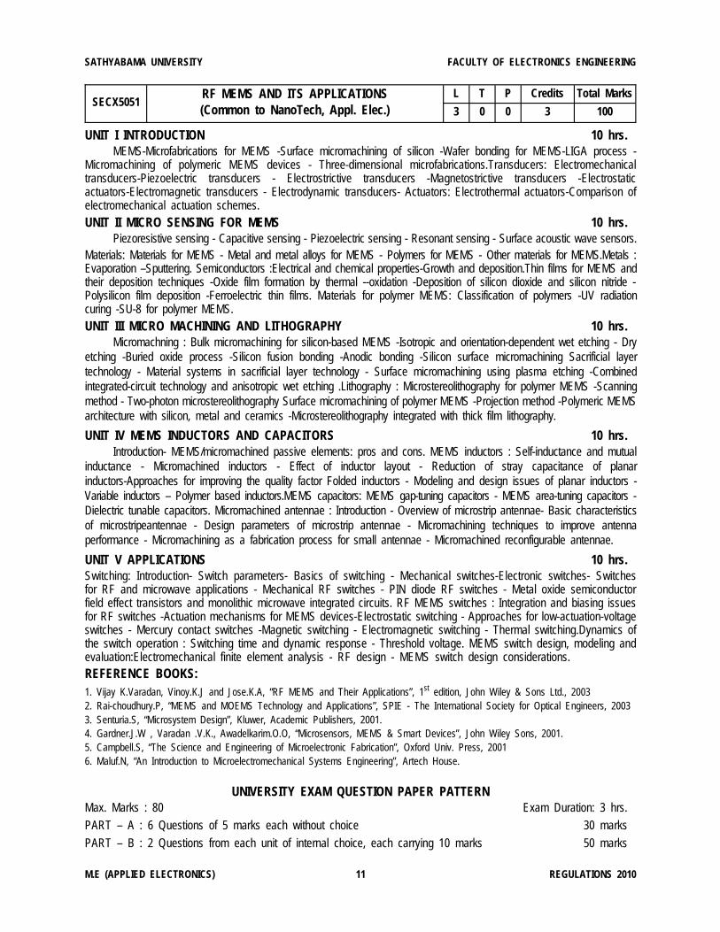
SECX5051RF MEMS AND ITS APPLICATIONS(Common to NanoTech, Appl. Elec.)
L T P Credits Total Marks
3 0 0 3 100
UNIT I INTRODUCTION 10 hrs.MEMS-Microfabrications for MEMS -Surface micromachining of silicon -Wafer bonding for MEMS-LIGA process -
Micromachining of polymeric MEMS devices - Three-dimensional microfabrications.Transducers: Electromechanicaltransducers-Piezoelectric transducers - Electrostrictive transducers -Magnetostrictive transducers -Electrostaticactuators-Electromagnetic transducers - Electrodynamic transducers- Actuators: Electrothermal actuators-Comparison ofelectromechanical actuation schemes.UNIT II MICRO SENSING FOR MEMS 10 hrs.
Piezoresistive sensing - Capacitive sensing - Piezoelectric sensing - Resonant sensing - Surface acoustic wave sensors.Materials: Materials for MEMS - Metal and metal alloys for MEMS - Polymers for MEMS - Other materials for MEMS.Metals :Evaporation –Sputtering. Semiconductors :Electrical and chemical properties-Growth and deposition.Thin films for MEMS andtheir deposition techniques -Oxide film formation by thermal --oxidation -Deposition of silicon dioxide and silicon nitride -Polysilicon film deposition -Ferroelectric thin films. Materials for polymer MEMS: Classification of polymers -UV radiationcuring -SU-8 for polymer MEMS.UNIT III MICRO MACHINING AND LITHOGRAPHY 10 hrs.
Micromachning : Bulk micromachining for silicon-based MEMS -Isotropic and orientation-dependent wet etching - Dryetching -Buried oxide process -Silicon fusion bonding -Anodic bonding -Silicon surface micromachining Sacrificial layertechnology - Material systems in sacrificial layer technology - Surface micromachining using plasma etching -Combinedintegrated-circuit technology and anisotropic wet etching .Lithography : Microstereolithography for polymer MEMS -Scanningmethod - Two-photon microstereolithography Surface micromachining of polymer MEMS -Projection method -Polymeric MEMSarchitecture with silicon, metal and ceramics -Microstereolithography integrated with thick film lithography.
UNIT IV MEMS INDUCTORS AND CAPACITORS 10 hrs.Introduction- MEMS/micromachined passive elements: pros and cons. MEMS inductors : Self-inductance and mutual
inductance - Micromachined inductors - Effect of inductor layout - Reduction of stray capacitance of planarinductors-Approaches for improving the quality factor Folded inductors - Modeling and design issues of planar inductors -Variable inductors – Polymer based inductors.MEMS capacitors: MEMS gap-tuning capacitors - MEMS area-tuning capacitors -Dielectric tunable capacitors. Micromachined antennae : Introduction - Overview of microstrip antennae- Basic characteristicsof microstripeantennae - Design parameters of microstrip antennae - Micromachining techniques to improve antennaperformance - Micromachining as a fabrication process for small antennae - Micromachined reconfigurable antennae.
UNIT V APPLICATIONS 10 hrs.Switching: Introduction- Switch parameters- Basics of switching - Mechanical switches-Electronic switches- Switchesfor RF and microwave applications - Mechanical RF switches - PIN diode RF switches - Metal oxide semiconductorfield effect transistors and monolithic microwave integrated circuits. RF MEMS switches : Integration and biasing issuesfor RF switches -Actuation mechanisms for MEMS devices-Electrostatic switching - Approaches for low-actuation-voltageswitches - Mercury contact switches -Magnetic switching - Electromagnetic switching - Thermal switching.Dynamics ofthe switch operation : Switching time and dynamic response - Threshold voltage. MEMS switch design, modeling andevaluation:Electromechanical finite element analysis - RF design - MEMS switch design considerations.REFERENCE BOOKS:1. Vijay K.Varadan, Vinoy.K.J and Jose.K.A, “RF MEMS and Their Applications”, 1st edition, John Wiley & Sons Ltd., 20032. Rai-choudhury.P, “MEMS and MOEMS Technology and Applications”, SPIE - The International Society for Optical Engineers, 20033. Senturia.S, “Microsystem Design”, Kluwer, Academic Publishers, 2001.4. Gardner.J.W , Varadan .V.K., Awadelkarim.O.O, “Microsensors, MEMS & Smart Devices”, John Wiley Sons, 2001.5. Campbell.S, “The Science and Engineering of Microelectronic Fabrication”, Oxford Univ. Press, 20016. Maluf.N, “An Introduction to Microelectromechanical Systems Engineering”, Artech House.
UNIVERSITY EXAM QUESTION PAPER PATTERNMax. Marks : 80 Exam Duration: 3 hrs.PART – A : 6 Questions of 5 marks each without choice 30 marks
PART – B : 2 Questions from each unit of internal choice, each carrying 10 marks 50 marks
SATHYABAMA UNIVERSITY FACULTY OF ELECTRONICS ENGINEERING
M.E (APPLIED ELECTRONICS) 11 REGULATIONS 2010
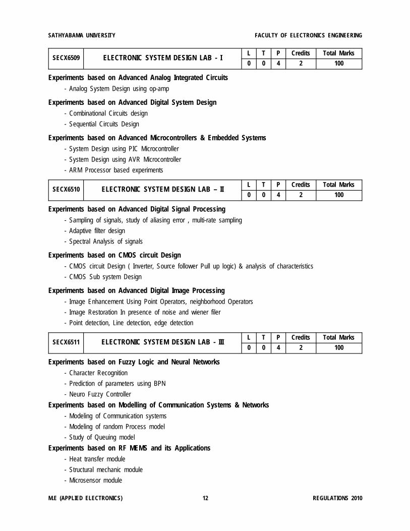
SECX6509 ELECTRONIC SYSTEM DESIGN LAB - IL T P Credits Total Marks
0 0 4 2 100
Experiments based on Advanced Analog Integrated Circuits- Analog System Design using op-amp
Experiments based on Advanced Digital System Design- Combinational Circuits design
- Sequential Circuits Design
Experiments based on Advanced Microcontrollers & Embedded Systems- System Design using PIC Microcontroller
- System Design using AVR Microcontroller
- ARM Processor based experiments
SECX6510 ELECTRONIC SYSTEM DESIGN LAB – IIL T P Credits Total Marks
0 0 4 2 100
Experiments based on Advanced Digital Signal Processing- Sampling of signals, study of aliasing error , multi-rate sampling
- Adaptive filter design
- Spectral Analysis of signals
Experiments based on CMOS circuit Design- CMOS circuit Design ( Inverter, Source follower Pull up logic) & analysis of characteristics
- CMOS Sub system Design
Experiments based on Advanced Digital Image Processing- Image Enhancement Using Point Operators, neighborhood Operators
- Image Restoration In presence of noise and wiener filer
- Point detection, Line detection, edge detection
SECX6511 ELECTRONIC SYSTEM DESIGN LAB - IIIL T P Credits Total Marks
0 0 4 2 100
Experiments based on Fuzzy Logic and Neural Networks- Character Recognition
- Prediction of parameters using BPN
- Neuro Fuzzy Controller
Experiments based on Modelling of Communication Systems & Networks- Modeling of Communication systems
- Modeling of random Process model
- Study of Queuing model
Experiments based on RF MEMS and its Applications- Heat transfer module
- Structural mechanic module
- Microsensor module
SATHYABAMA UNIVERSITY FACULTY OF ELECTRONICS ENGINEERING
M.E (APPLIED ELECTRONICS) 12 REGULATIONS 2010
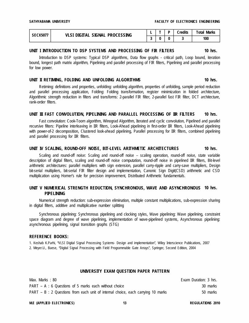
SECX5077 VLSI DIGITAL SIGNAL PROCESSINGL T P Credits Total Marks
3 0 0 3 100
UNIT I INTRODUCTION TO DSP SYSTEMS AND PROCESSING OF FIR FILTERS 10 hrs.
Introduction to DSP systems: Typical DSP algorithms, Data flow graphs - critical path, Loop bound, iterationbound, longest path matrix algorithm, Pipelining and parallel processing of FIR filters, Pipelining and parallel processingfor low power.
UNIT II RETIMING, FOLDING AND UNFOLDING ALGORITHMS 10 hrs.
Retiming: definitions and properties, unfolding: unfolding algorithm, properties of unfolding, sample period reductionand parallel processing application, Folding: Folding transformation, register minimization in folded architecture,Algorithmic strength reduction in filters and transforms: 2-parallel FIR filter, 2-parallel fast FIR filter, DCT architecture,rank-order filters.
UNIT III FAST CONVOLUTION, PIPELINING AND PARALLEL PROCESSING OF IIR FILTERS 10 hrs.
Fast convolution: Cook-Toom algorithm, Winograd Algorithm, Iterated and cyclic convolution, Pipelined and parallelrecursive filters: Pipeline interleaving in IIR filters, Look-Ahead pipelining in first-order IIR filters, Look-Ahead pipeliningwith power-of-2 decomposition, Clustered look-ahead pipelining, Parallel processing for IIR filters, combined pipeliningand parallel processing for IIR filters.
UNIT IV SCALING, ROUND-OFF NOISE, BIT-LEVEL ARITHMETIC ARCHITECTURES 10 hrs.
Scaling and round-off noise: Scaling and round-off noise – scaling operation, round-off noise, state variabledescription of digital filters, scaling and round-off noise computation, round-off noise in pipelined IIR filters, Bit-levelarithmetic architectures: parallel multipliers with sign extension, parallel carry-ripple and carry-save multipliers, Designbit-serial multipliers, bit-serial FIR filter design and implementation, Canonic Sign Digit(CSD) arithmetic and CSDmultiplication using Horner’s rule for precision improvement, Distributed Arithmetic fundamentals.
UNIT V NUMERICAL STRENGTH REDUCTION, SYNCHRONOUS, WAVE AND ASYNCHRONOUS PIPELINING
10 hrs.
Numerical strength reduction: sub-expression elimination, multiple constant multiplications, sub-expression sharingin digital filters, additive and multiplicative number splitting
Synchronous pipelining: Synchronous pipelining and clocking styles, Wave pipelining: Wave pipelining, constraintspace diagram and degree of wave pipelining, implementation of wave-pipelined systems, Asynchronous pipelining:asynchronous pipelining, signal transition graphs (STG)
REFERENCE BOOKS:1. Keshab K.Parhi, “VLSI Digital Signal Processing Systems- Design and implementation”, Wiley Interscience Publications, 20072. Meyer.U., Baese, “Digital Signal Processing with Field Programmable Gate Arrays”, Springer, Second Edition, 2004
UNIVERSITY EXAM QUESTION PAPER PATTERN
Max. Marks : 80 Exam Duration: 3 hrs.PART – A : 6 Questions of 5 marks each without choice 30 marks
PART – B : 2 Questions from each unit of internal choice, each carrying 10 marks 50 marks
SATHYABAMA UNIVERSITY FACULTY OF ELECTRONICS ENGINEERING
M.E (APPLIED ELECTRONICS) 13 REGULATIONS 2010
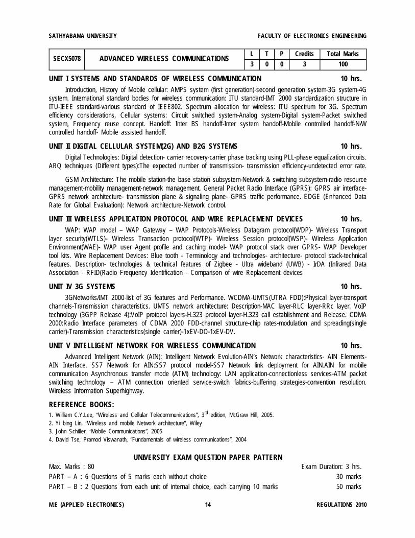
SECX5078 ADVANCED WIRELESS COMMUNICATIONSL T P Credits Total Marks
3 0 0 3 100
UNIT I SYSTEMS AND STANDARDS OF WIRELESS COMMUNICATION 10 hrs.Introduction, History of Mobile cellular: AMPS system (first generation)-second generation system-3G system-4G
system. International standard bodies for wireless communication: ITU standard-IMT 2000 standardization structure inITU-IEEE standard-various standard of IEEE802. Spectrum allocation for wireless: ITU spectrum for 3G. Spectrumefficiency considerations, Cellular systems: Circuit switched system-Analog system-Digital system-Packet switchedsystem, Frequency reuse concept. Handoff: Inter BS handoff-Inter system handoff-Mobile controlled handoff-N/Wcontrolled handoff- Mobile assisted handoff.
UNIT II DIGITAL CELLULAR SYSTEM(2G) AND B2G SYSTEMS 10 hrs.Digital Technologies: Digital detection- carrier recovery-carrier phase tracking using PLL-phase equalization circuits.
ARQ techniques (Different types):The expected number of transmission- transmission efficiency-undetected error rate.
GSM Architecture: The mobile station-the base station subsystem-Network & switching subsystem-radio resourcemanagement-mobility management-network management. General Packet Radio Interface (GPRS): GPRS air interface-GPRS network architecture- transmission plane & signaling plane- GPRS traffic performance. EDGE (Enhanced DataRate for Global Evaluation): Network architecture-Network control.
UNIT III WIRELESS APPLICATION PROTOCOL AND WIRE REPLACEMENT DEVICES 10 hrs.WAP: WAP model – WAP Gateway – WAP Protocols-Wireless Datagram protocol(WDP)- Wireless Transport
layer security(WTLS)- Wireless Transaction protocol(WTP)- Wireless Session protocol(WSP)- Wireless ApplicationEnvironment(WAE)- WAP user Agent profile and caching model- WAP protocol stack over GPRS- WAP Developertool kits. Wire Replacement Devices: Blue tooth - Terminology and technologies- architecture- protocol stack-technicalfeatures. Description- technologies & technical features of Zigbee - Ultra wideband (UWB) - IrDA (Infrared DataAssociation - RFID(Radio Frequency Identification - Comparison of wire Replacement devices
UNIT IV 3G SYSTEMS 10 hrs.3GNetworks/IMT 2000-list of 3G features and Performance. WCDMA-UMTS(UTRA FDD):Physical layer-transport
channels-Transmission characteristics. UMTS network architecture: Description-MAC layer-RLC layer-RRc layer. VoIPtechnology (3GPP Release 4):VoIP protocol layers-H.323 protocol layer-H.323 call establishment and Release. CDMA2000:Radio Interface parameters of CDMA 2000 FDD-channel structure-chip rates-modulation and spreading(singlecarrier)-Transmission characteristics(single carrier)-1xEV-DO-1xEV-DV.
UNIT V INTELLIGENT NETWORK FOR WIRELESS COMMUNICATION 10 hrs.Advanced Intelligent Network (AIN): Intelligent Network Evolution-AIN’s Network characteristics- AIN Elements-
AIN Interface. SS7 Network for AIN:SS7 protocol model-SS7 Network link deployment for AIN.AIN for mobilecommunication Asynchronous transfer mode (ATM) technology: LAN application-connectionless services-ATM packetswitching technology – ATM connection oriented service-switch fabrics-buffering strategies-convention resolution.Wireless Information Superhighway.
REFERENCE BOOKS:1. William C.Y.Lee, “Wireless and Cellular Telecommunications”, 3rd edition, McGraw Hill, 2005.2. Yi bing Lin, “Wireless and mobile Network architecture”, Wiley3. John Schiller, “Mobile Communications”, 20054. David Tse, Pramod Viswanath, “Fundamentals of wireless communications”, 2004
UNIVERSITY EXAM QUESTION PAPER PATTERNMax. Marks : 80 Exam Duration: 3 hrs.PART – A : 6 Questions of 5 marks each without choice 30 marksPART – B : 2 Questions from each unit of internal choice, each carrying 10 marks 50 marks
SATHYABAMA UNIVERSITY FACULTY OF ELECTRONICS ENGINEERING
M.E (APPLIED ELECTRONICS) 14 REGULATIONS 2010
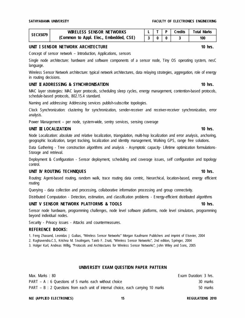
SECX5079WIRELESS SENSOR NETWORKS
(Common to Appl. Elec., Embedded, CSE)L T P Credits Total Marks
3 0 0 3 100
UNIT I SENSOR NETWORK ARCHITECTURE 10 hrs.Concept of sensor network – Introduction, Applications, sensors
Single node architecture: hardware and software components of a sensor node, Tiny OS operating system, nesClanguage.
Wireless Sensor Network architecture: typical network architectures, data relaying strategies, aggregation, role of energyin routing decisions.
UNIT II ADDRESSING & SYNCHRONISATION 10 hrs.MAC layer strategies: MAC layer protocols, scheduling sleep cycles, energy management, contention-based protocols,schedule-based protocols, 802.15.4 standard.
Naming and addressing: Addressing services publish-subscribe topologies.
Clock Synchronization: clustering for synchronization, sender-receiver and receiver-receiver synchronization, erroranalysis.
Power Management – per node, system-wide, sentry services, sensing coverage
UNIT III LOCALIZATION 10 hrs.Node Localization: absolute and relative localization, triangulation, multi-hop localization and error analysis, anchoring,geographic localization, target tracking, localization and identity management, Walking GPS, range free solutions.
Data Gathering - Tree construction algorithms and analysis - Asymptotic capacity- Lifetime optimization formulations-Storage and retrieval.
Deployment & Configuration - Sensor deployment, scheduling and coverage issues, self configuration and topologycontrol.
UNIT IV ROUTING TECHNIQUES 10 hrs.Routing: Agent-based routing, random walk, trace routing data centric, hierarchical, location-based, energy efficientrouting
Querying - data collection and processing, collaborative information processing and group connectivity.
Distributed Computation - Detection, estimation, and classification problems - Energy-efficient distributed algorithms
UNIT V SENSOR NETWORK PLATFORMS & TOOLS 10 hrs.Sensor node hardware, programming challenges, node level software platforms, node level simulators, programmingbeyond individual nodes.
Security - Privacy issues - Attacks and countermeasures.
REFERENCE BOOKS:1. Feng Zhaoand, Leonidas J Guibas, “Wireless Sensor Networks” Morgan Kaufmann Publishers and imprint of Elsevier, 20042. Raghavendra.C.S, Krishna M. Sivalingam, Taieb F. Znati, “Wireless Sensor Networks”, 2nd edition, Springer, 20043. Holger Karl, Andreas Willig, “Protocols and Architectures for Wireless Sensor Networks”, John Wiley and Sons, 2005
UNIVERSITY EXAM QUESTION PAPER PATTERN
Max. Marks : 80 Exam Duration: 3 hrs.PART – A : 6 Questions of 5 marks each without choice 30 marksPART – B : 2 Questions from each unit of internal choice, each carrying 10 marks 50 marks
SATHYABAMA UNIVERSITY FACULTY OF ELECTRONICS ENGINEERING
M.E (APPLIED ELECTRONICS) 15 REGULATIONS 2010
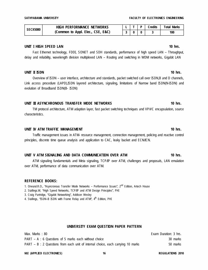
SECX5080HIGH PERFORMANCE NETWORKS
(Common to Appl. Elec., CSE, E&C)L T P Credits Total Marks
3 0 0 3 100
UNIT I HIGH SPEED LAN 10 hrs.
Fast Ethernet technology, FDDI, SONET and SDH standards, performance of high speed LAN – Throughput,delay and reliability, wavelength division multiplexed LAN – Routing and switching in WDM networks, Gigabit LAN
UNIT II ISDN 10 hrs.
Overview of ISDN – user interface, architecture and standards, packet switched call over ISDN,B and D channels,Link access procedure (LAPD),ISDN layered architecture, signaling, limitations of Narrow band ISDN(N-ISDN) andevolution of Broadband ISDN(B- ISDN)
UNIT III ASYNCHRONOUS TRANSFER MODE NETWORKS 10 hrs.
TM protocol architecture, ATM adaption layer, fast packet switching techniques and VP/VC encapsulation, sourcecharacteristics.
UNIT IV ATM TRAFFIC MANAGEMENT 10 hrs.
Traffic management issues in ATM- resource management, connection management, policing and reactive controlprinciples, discrete time queue analysis and application to CAC, leaky bucket and ECN/ICN.
UNIT V ATM SIGNALING AND DATA COMMUNICATION OVER ATM 10 hrs.
ATM signaling fundamentals and Meta signaling, TCP/IP over ATM, challenges and proposals, LAN emulationover ATM, performance of data communication over ATM.
REFERENCE BOOKS:1. Onvural.R.O., “Asyncronous Transfer Mode Networks – Performance Issues”, 2nd Edition, Artech House2. Stallings.W, “High Speed Networks, TCP/IP and ATM Design Principles”, PHI3. Craig Partridge, “Gigabit Networking”, Addison Wesley4. Stallings, “ISDN–B ISDN with Frame Relay and ATM”, 4th Edition, PHI
UNIVERSITY EXAM QUESTION PAPER PATTERN
Max. Marks : 80 Exam Duration: 3 hrs.
PART – A : 6 Questions of 5 marks each without choice 30 marks
PART – B : 2 Questions from each unit of internal choice, each carrying 10 marks 50 marks
SATHYABAMA UNIVERSITY FACULTY OF ELECTRONICS ENGINEERING
M.E (APPLIED ELECTRONICS) 16 REGULATIONS 2010
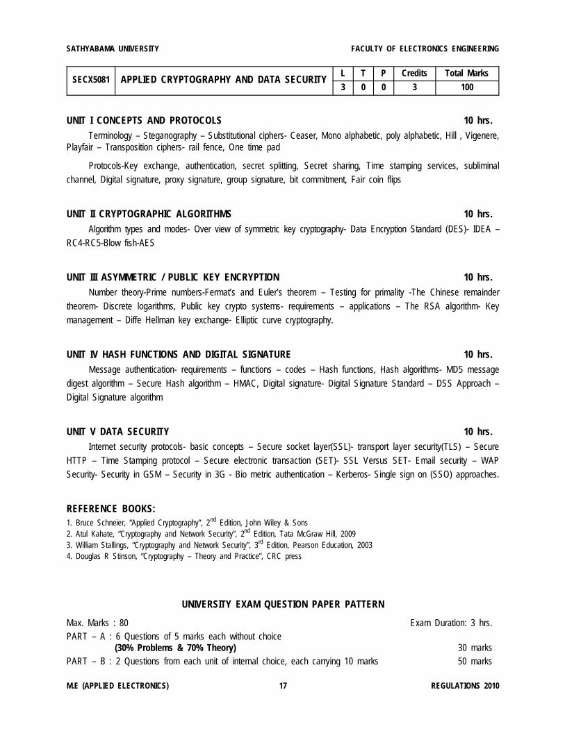
SECX5081 APPLIED CRYPTOGRAPHY AND DATA SECURITYL T P Credits Total Marks
3 0 0 3 100
UNIT I CONCEPTS AND PROTOCOLS 10 hrs.Terminology – Steganography – Substitutional ciphers- Ceaser, Mono alphabetic, poly alphabetic, Hill , Vigenere,
Playfair – Transposition ciphers- rail fence, One time pad
Protocols-Key exchange, authentication, secret splitting, Secret sharing, Time stamping services, subliminalchannel, Digital signature, proxy signature, group signature, bit commitment, Fair coin flips
UNIT II CRYPTOGRAPHIC ALGORITHMS 10 hrs.Algorithm types and modes- Over view of symmetric key cryptography- Data Encryption Standard (DES)- IDEA –
RC4-RC5-Blow fish-AES
UNIT III ASYMMETRIC / PUBLIC KEY ENCRYPTION 10 hrs.Number theory-Prime numbers-Fermat’s and Euler’s theorem – Testing for primality -The Chinese remainder
theorem- Discrete logarithms, Public key crypto systems- requirements – applications – The RSA algorithm- Keymanagement – Diffe Hellman key exchange- Elliptic curve cryptography.
UNIT IV HASH FUNCTIONS AND DIGITAL SIGNATURE 10 hrs.Message authentication- requirements – functions – codes – Hash functions, Hash algorithms- MD5 message
digest algorithm – Secure Hash algorithm – HMAC, Digital signature- Digital Signature Standard – DSS Approach –Digital Signature algorithm
UNIT V DATA SECURITY 10 hrs.Internet security protocols- basic concepts – Secure socket layer(SSL)- transport layer security(TLS) – Secure
HTTP – Time Stamping protocol – Secure electronic transaction (SET)- SSL Versus SET- Email security – WAPSecurity- Security in GSM – Security in 3G - Bio metric authentication – Kerberos- Single sign on (SSO) approaches.
REFERENCE BOOKS:1. Bruce Schneier, “Applied Cryptography”, 2nd Edition, John Wiley & Sons2. Atul Kahate, “Cryptography and Network Security”, 2nd Edition, Tata McGraw Hill, 20093. William Stallings, “Cryptography and Network Security”, 3rd Edition, Pearson Education, 2003 4. Douglas R Stinson, “Cryptography – Theory and Practice”, CRC press
UNIVERSITY EXAM QUESTION PAPER PATTERN
Max. Marks : 80 Exam Duration: 3 hrs.PART – A : 6 Questions of 5 marks each without choice (30% Problems & 70% Theory) 30 marksPART – B : 2 Questions from each unit of internal choice, each carrying 10 marks 50 marks
SATHYABAMA UNIVERSITY FACULTY OF ELECTRONICS ENGINEERING
M.E (APPLIED ELECTRONICS) 17 REGULATIONS 2010
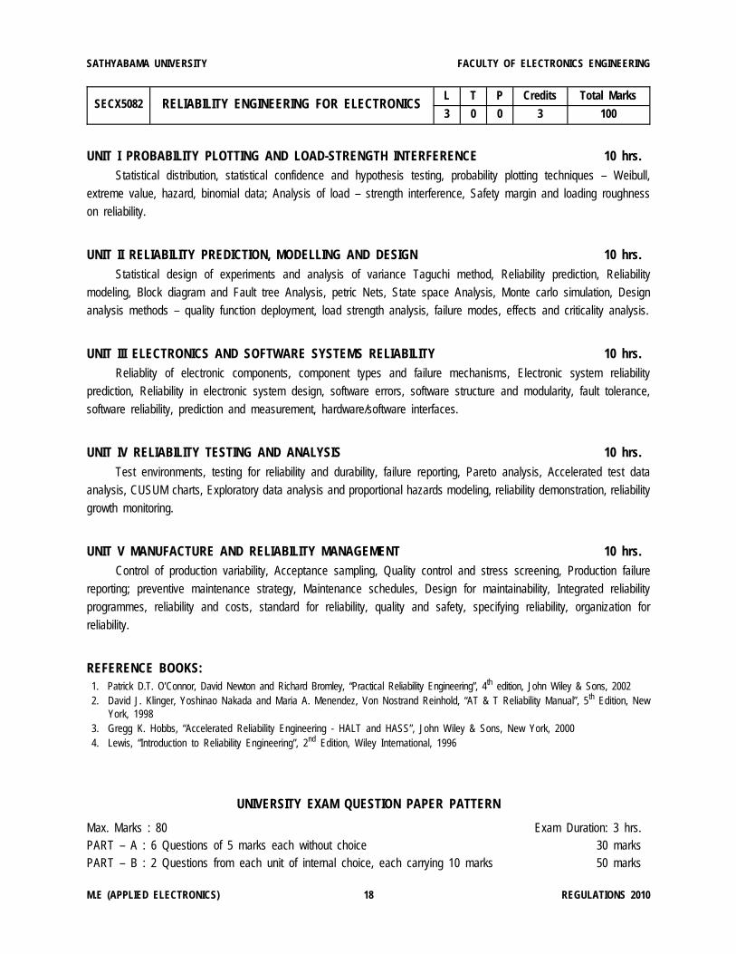
SECX5082 RELIABILITY ENGINEERING FOR ELECTRONICSL T P Credits Total Marks
3 0 0 3 100
UNIT I PROBABILITY PLOTTING AND LOAD-STRENGTH INTERFERENCE 10 hrs.Statistical distribution, statistical confidence and hypothesis testing, probability plotting techniques – Weibull,
extreme value, hazard, binomial data; Analysis of load – strength interference, Safety margin and loading roughnesson reliability.
UNIT II RELIABILITY PREDICTION, MODELLING AND DESIGN 10 hrs.Statistical design of experiments and analysis of variance Taguchi method, Reliability prediction, Reliability
modeling, Block diagram and Fault tree Analysis, petric Nets, State space Analysis, Monte carlo simulation, Designanalysis methods – quality function deployment, load strength analysis, failure modes, effects and criticality analysis.
UNIT III ELECTRONICS AND SOFTWARE SYSTEMS RELIABILITY 10 hrs.Reliablity of electronic components, component types and failure mechanisms, Electronic system reliability
prediction, Reliability in electronic system design, software errors, software structure and modularity, fault tolerance,software reliability, prediction and measurement, hardware/software interfaces.
UNIT IV RELIABILITY TESTING AND ANALYSIS 10 hrs.Test environments, testing for reliability and durability, failure reporting, Pareto analysis, Accelerated test data
analysis, CUSUM charts, Exploratory data analysis and proportional hazards modeling, reliability demonstration, reliabilitygrowth monitoring.
UNIT V MANUFACTURE AND RELIABILITY MANAGEMENT 10 hrs.Control of production variability, Acceptance sampling, Quality control and stress screening, Production failure
reporting; preventive maintenance strategy, Maintenance schedules, Design for maintainability, Integrated reliabilityprogrammes, reliability and costs, standard for reliability, quality and safety, specifying reliability, organization forreliability.
REFERENCE BOOKS: 1. Patrick D.T. O’Connor, David Newton and Richard Bromley, “Practical Reliability Engineering”, 4th edition, John Wiley & Sons, 2002 2. David J. Klinger, Yoshinao Nakada and Maria A. Menendez, Von Nostrand Reinhold, “AT & T Reliability Manual”, 5th Edition, New
York, 1998 3. Gregg K. Hobbs, “Accelerated Reliability Engineering - HALT and HASS”, John Wiley & Sons, New York, 2000 4. Lewis, “Introduction to Reliability Engineering”, 2nd Edition, Wiley International, 1996
UNIVERSITY EXAM QUESTION PAPER PATTERN
Max. Marks : 80 Exam Duration: 3 hrs.PART – A : 6 Questions of 5 marks each without choice 30 marksPART – B : 2 Questions from each unit of internal choice, each carrying 10 marks 50 marks
SATHYABAMA UNIVERSITY FACULTY OF ELECTRONICS ENGINEERING
M.E (APPLIED ELECTRONICS) 18 REGULATIONS 2010
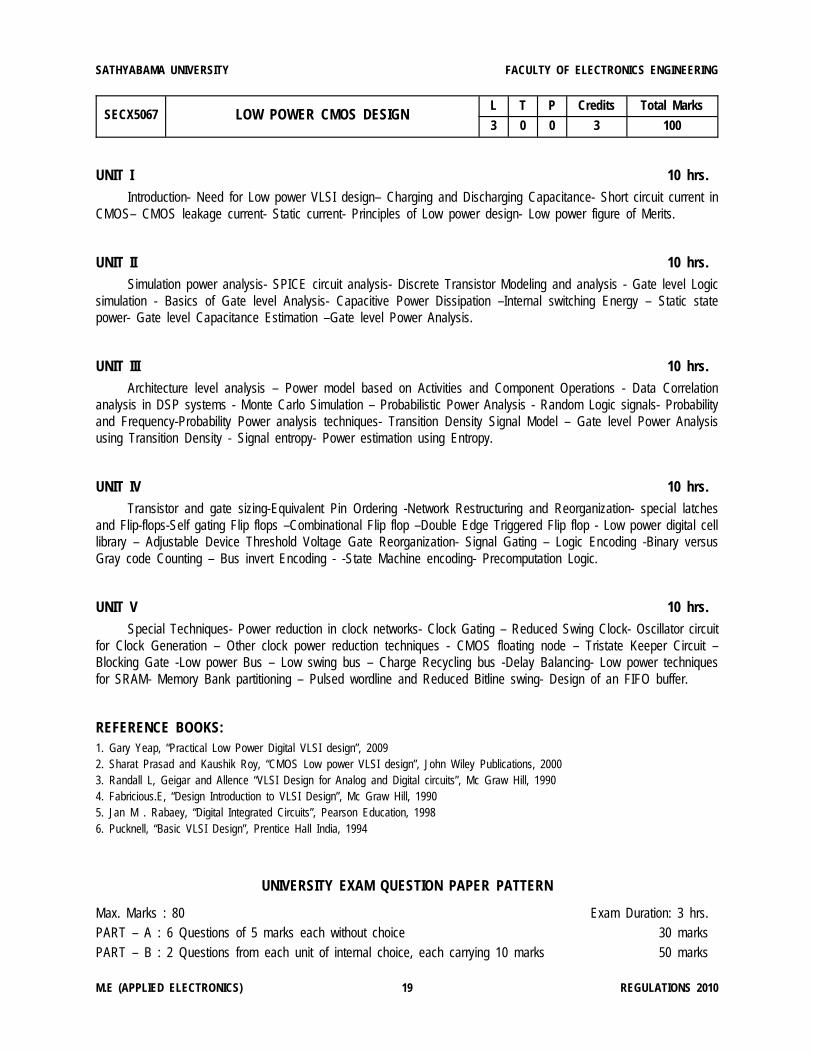
SECX5067 LOW POWER CMOS DESIGNL T P Credits Total Marks
3 0 0 3 100
UNIT I 10 hrs.Introduction- Need for Low power VLSI design– Charging and Discharging Capacitance- Short circuit current in
CMOS– CMOS leakage current- Static current- Principles of Low power design- Low power figure of Merits.
UNIT II 10 hrs.Simulation power analysis- SPICE circuit analysis- Discrete Transistor Modeling and analysis - Gate level Logic
simulation - Basics of Gate level Analysis- Capacitive Power Dissipation –Internal switching Energy – Static statepower- Gate level Capacitance Estimation –Gate level Power Analysis.
UNIT III 10 hrs.Architecture level analysis – Power model based on Activities and Component Operations - Data Correlation
analysis in DSP systems - Monte Carlo Simulation – Probabilistic Power Analysis - Random Logic signals- Probabilityand Frequency-Probability Power analysis techniques- Transition Density Signal Model – Gate level Power Analysisusing Transition Density - Signal entropy- Power estimation using Entropy.
UNIT IV 10 hrs.Transistor and gate sizing-Equivalent Pin Ordering -Network Restructuring and Reorganization- special latches
and Flip-flops-Self gating Flip flops –Combinational Flip flop –Double Edge Triggered Flip flop - Low power digital celllibrary – Adjustable Device Threshold Voltage Gate Reorganization- Signal Gating – Logic Encoding -Binary versusGray code Counting – Bus invert Encoding - -State Machine encoding- Precomputation Logic.
UNIT V 10 hrs.Special Techniques- Power reduction in clock networks- Clock Gating – Reduced Swing Clock- Oscillator circuit
for Clock Generation – Other clock power reduction techniques - CMOS floating node – Tristate Keeper Circuit –Blocking Gate -Low power Bus – Low swing bus – Charge Recycling bus -Delay Balancing- Low power techniquesfor SRAM- Memory Bank partitioning – Pulsed wordline and Reduced Bitline swing- Design of an FIFO buffer.
REFERENCE BOOKS:1. Gary Yeap, “Practical Low Power Digital VLSI design”, 20092. Sharat Prasad and Kaushik Roy, “CMOS Low power VLSI design”, John Wiley Publications, 20003. Randall L, Geigar and Allence “VLSI Design for Analog and Digital circuits”, Mc Graw Hill, 19904. Fabricious.E, “Design Introduction to VLSI Design”, Mc Graw Hill, 19905. Jan M . Rabaey, “Digital Integrated Circuits”, Pearson Education, 19986. Pucknell, “Basic VLSI Design”, Prentice Hall India, 1994
UNIVERSITY EXAM QUESTION PAPER PATTERN
Max. Marks : 80 Exam Duration: 3 hrs.PART – A : 6 Questions of 5 marks each without choice 30 marksPART – B : 2 Questions from each unit of internal choice, each carrying 10 marks 50 marks
SATHYABAMA UNIVERSITY FACULTY OF ELECTRONICS ENGINEERING
M.E (APPLIED ELECTRONICS) 19 REGULATIONS 2010
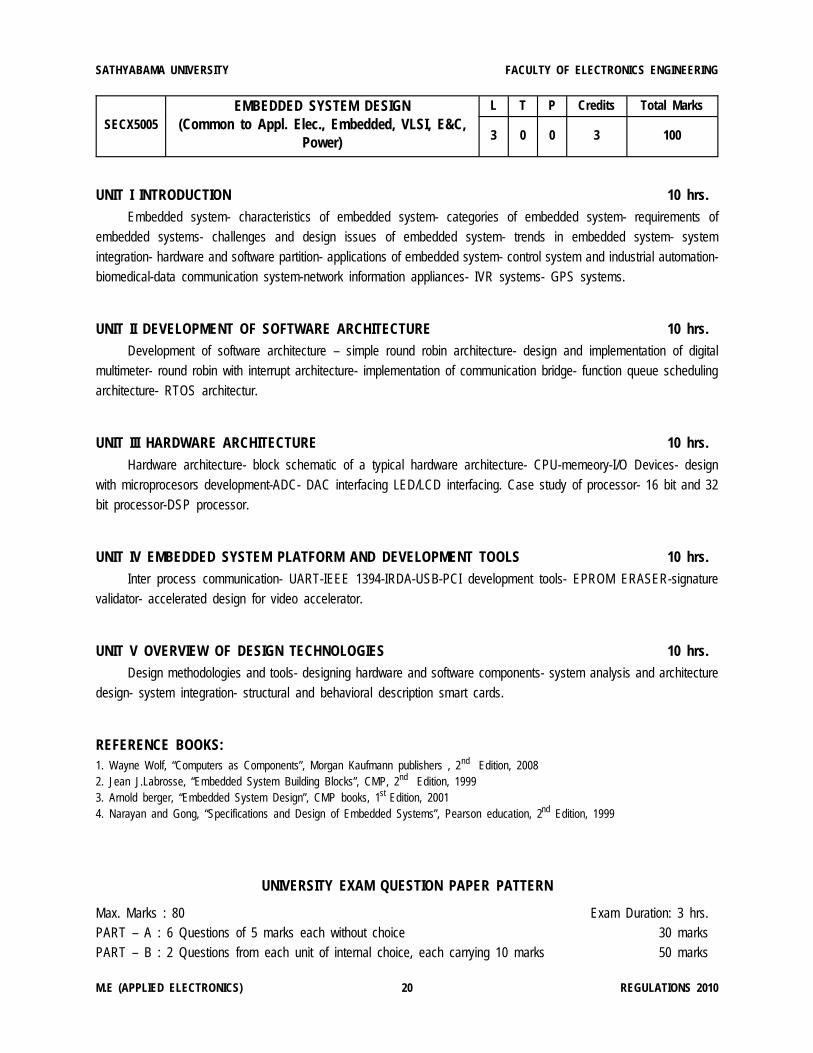
SECX5005EMBEDDED SYSTEM DESIGN
(Common to Appl. Elec., Embedded, VLSI, E&C,Power)
L T P Credits Total Marks
3 0 0 3 100
UNIT I INTRODUCTION 10 hrs.Embedded system- characteristics of embedded system- categories of embedded system- requirements of
embedded systems- challenges and design issues of embedded system- trends in embedded system- systemintegration- hardware and software partition- applications of embedded system- control system and industrial automation-biomedical-data communication system-network information appliances- IVR systems- GPS systems.
UNIT II DEVELOPMENT OF SOFTWARE ARCHITECTURE 10 hrs.Development of software architecture – simple round robin architecture- design and implementation of digital
multimeter- round robin with interrupt architecture- implementation of communication bridge- function queue schedulingarchitecture- RTOS architectur.
UNIT III HARDWARE ARCHITECTURE 10 hrs.Hardware architecture- block schematic of a typical hardware architecture- CPU-memeory-I/O Devices- design
with microprocesors development-ADC- DAC interfacing LED/LCD interfacing. Case study of processor- 16 bit and 32bit processor-DSP processor.
UNIT IV EMBEDDED SYSTEM PLATFORM AND DEVELOPMENT TOOLS 10 hrs.Inter process communication- UART-IEEE 1394-IRDA-USB-PCI development tools- EPROM ERASER-signature
validator- accelerated design for video accelerator.
UNIT V OVERVIEW OF DESIGN TECHNOLOGIES 10 hrs.Design methodologies and tools- designing hardware and software components- system analysis and architecture
design- system integration- structural and behavioral description smart cards.
REFERENCE BOOKS:1. Wayne Wolf, “Computers as Components”, Morgan Kaufmann publishers , 2nd Edition, 20082. Jean J.Labrosse, “Embedded System Building Blocks”, CMP, 2nd Edition, 19993. Arnold berger, “Embedded System Design”, CMP books, 1st Edition, 20014. Narayan and Gong, “Specifications and Design of Embedded Systems”, Pearson education, 2nd Edition, 1999
UNIVERSITY EXAM QUESTION PAPER PATTERN
Max. Marks : 80 Exam Duration: 3 hrs.PART – A : 6 Questions of 5 marks each without choice 30 marksPART – B : 2 Questions from each unit of internal choice, each carrying 10 marks 50 marks
SATHYABAMA UNIVERSITY FACULTY OF ELECTRONICS ENGINEERING
M.E (APPLIED ELECTRONICS) 20 REGULATIONS 2010
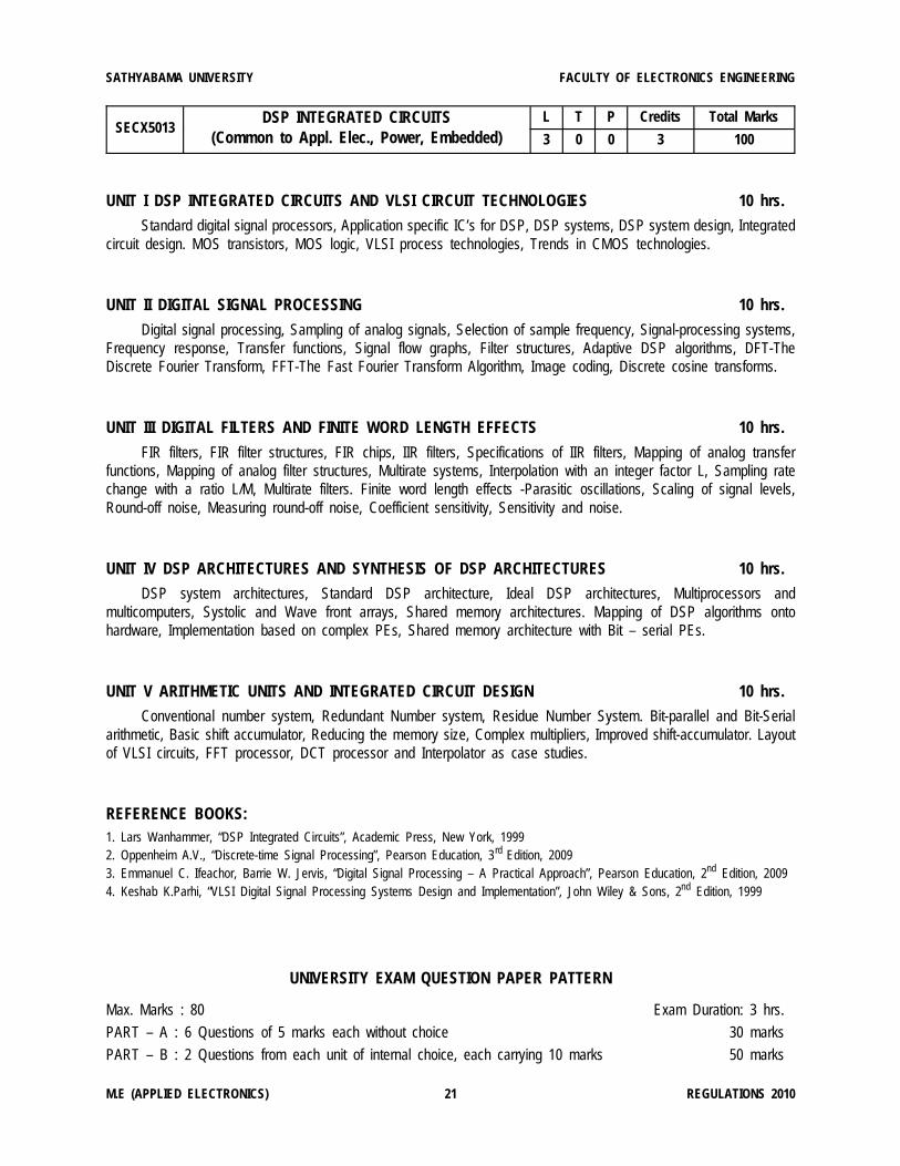
SECX5013DSP INTEGRATED CIRCUITS
(Common to Appl. Elec., Power, Embedded)L T P Credits Total Marks
3 0 0 3 100
UNIT I DSP INTEGRATED CIRCUITS AND VLSI CIRCUIT TECHNOLOGIES 10 hrs.
Standard digital signal processors, Application specific IC’s for DSP, DSP systems, DSP system design, Integratedcircuit design. MOS transistors, MOS logic, VLSI process technologies, Trends in CMOS technologies.
UNIT II DIGITAL SIGNAL PROCESSING 10 hrs.
Digital signal processing, Sampling of analog signals, Selection of sample frequency, Signal-processing systems,Frequency response, Transfer functions, Signal flow graphs, Filter structures, Adaptive DSP algorithms, DFT-TheDiscrete Fourier Transform, FFT-The Fast Fourier Transform Algorithm, Image coding, Discrete cosine transforms.
UNIT III DIGITAL FILTERS AND FINITE WORD LENGTH EFFECTS 10 hrs.
FIR filters, FIR filter structures, FIR chips, IIR filters, Specifications of IIR filters, Mapping of analog transferfunctions, Mapping of analog filter structures, Multirate systems, Interpolation with an integer factor L, Sampling ratechange with a ratio L/M, Multirate filters. Finite word length effects -Parasitic oscillations, Scaling of signal levels,Round-off noise, Measuring round-off noise, Coefficient sensitivity, Sensitivity and noise.
UNIT IV DSP ARCHITECTURES AND SYNTHESIS OF DSP ARCHITECTURES 10 hrs.
DSP system architectures, Standard DSP architecture, Ideal DSP architectures, Multiprocessors andmulticomputers, Systolic and Wave front arrays, Shared memory architectures. Mapping of DSP algorithms ontohardware, Implementation based on complex PEs, Shared memory architecture with Bit – serial PEs.
UNIT V ARITHMETIC UNITS AND INTEGRATED CIRCUIT DESIGN 10 hrs.
Conventional number system, Redundant Number system, Residue Number System. Bit-parallel and Bit-Serialarithmetic, Basic shift accumulator, Reducing the memory size, Complex multipliers, Improved shift-accumulator. Layoutof VLSI circuits, FFT processor, DCT processor and Interpolator as case studies.
REFERENCE BOOKS:1. Lars Wanhammer, “DSP Integrated Circuits”, Academic Press, New York, 19992. Oppenheim A.V., “Discrete-time Signal Processing”, Pearson Education, 3rd Edition, 20093. Emmanuel C. Ifeachor, Barrie W. Jervis, “Digital Signal Processing – A Practical Approach”, Pearson Education, 2nd Edition, 20094. Keshab K.Parhi, “VLSI Digital Signal Processing Systems Design and Implementation”, John Wiley & Sons, 2nd Edition, 1999
UNIVERSITY EXAM QUESTION PAPER PATTERN
Max. Marks : 80 Exam Duration: 3 hrs.
PART – A : 6 Questions of 5 marks each without choice 30 marks
PART – B : 2 Questions from each unit of internal choice, each carrying 10 marks 50 marks
SATHYABAMA UNIVERSITY FACULTY OF ELECTRONICS ENGINEERING
M.E (APPLIED ELECTRONICS) 21 REGULATIONS 2010
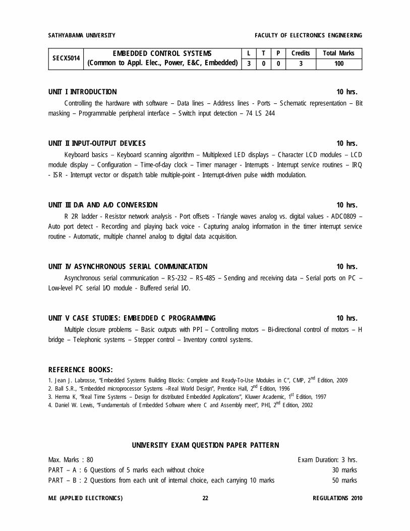
SECX5014EMBEDDED CONTROL SYSTEMS
(Common to Appl. Elec., Power, E&C, Embedded)L T P Credits Total Marks
3 0 0 3 100
UNIT I INTRODUCTION 10 hrs.
Controlling the hardware with software – Data lines – Address lines - Ports – Schematic representation – Bitmasking – Programmable peripheral interface – Switch input detection – 74 LS 244
UNIT II INPUT-OUTPUT DEVICES 10 hrs.
Keyboard basics – Keyboard scanning algorithm – Multiplexed LED displays – Character LCD modules – LCDmodule display – Configuration – Time-of-day clock – Timer manager - Interrupts - Interrupt service routines – IRQ- ISR - Interrupt vector or dispatch table multiple-point - Interrupt-driven pulse width modulation.
UNIT III D/A AND A/D CONVERSION 10 hrs.
R 2R ladder - Resistor network analysis - Port offsets - Triangle waves analog vs. digital values - ADC0809 –Auto port detect - Recording and playing back voice - Capturing analog information in the timer interrupt serviceroutine - Automatic, multiple channel analog to digital data acquisition.
UNIT IV ASYNCHRONOUS SERIAL COMMUNICATION 10 hrs.
Asynchronous serial communication – RS-232 – RS-485 – Sending and receiving data – Serial ports on PC –Low-level PC serial I/O module - Buffered serial I/O.
UNIT V CASE STUDIES: EMBEDDED C PROGRAMMING 10 hrs.
Multiple closure problems – Basic outputs with PPI – Controlling motors – Bi-directional control of motors – Hbridge – Telephonic systems – Stepper control – Inventory control systems.
REFERENCE BOOKS:1. Jean J. Labrosse, “Embedded Systems Building Blocks: Complete and Ready-To-Use Modules in C”, CMP, 2nd Edition, 20092. Ball S.R., “Embedded microprocessor Systems –Real World Design”, Prentice Hall, 2nd Edition, 19963. Herma K, “Real Time Systems – Design for distributed Embedded Applications”, Kluwer Academic, 1st Edition, 19974. Daniel W. Lewis, “Fundamentals of Embedded Software where C and Assembly meet”, PHI, 2nd Edition, 2002
UNIVERSITY EXAM QUESTION PAPER PATTERN
Max. Marks : 80 Exam Duration: 3 hrs.
PART – A : 6 Questions of 5 marks each without choice 30 marks
PART – B : 2 Questions from each unit of internal choice, each carrying 10 marks 50 marks
SATHYABAMA UNIVERSITY FACULTY OF ELECTRONICS ENGINEERING
M.E (APPLIED ELECTRONICS) 22 REGULATIONS 2010
SECX5031ELECTROMAGNETIC INTERFERENCE &
COMPATIBILITY(Common to Appl. Elec., E&C, VLSI, Embedded)
L T P Credits Total Marks
3 0 0 3 100
UNIT I EMI ENVIRONMENT 10 hrs.Introduction to EMI/EMC-Basics of electro Magnetic interference (EMI) Fundamentals of electromagnetic
compatibility (EMC)-Radiation hazards Transients and other EMI sources Transients Electrostatics discharge(ESD)-Tempest- Lightning
UNIT II EMI COUPLING 10 hrs.EMI from apparatus and circuits: Introduction-Electromagnetic emission-Appliances-noise from relays and
switches-nonlinearities in circuits-Passive inter modulation-Cross talk in transmission lines-Transmission in power supplylines-Electromagnetic interference.
UNIT III EMI SPECIFICATION/STANDARDS AND MEASUREMENTS 10 hrs.Units of specification - civilian standards and military standards. Basics of EMI measurements-EMI measurement
tools-TEM cell-measurement using TEM cell-Reverberating chamber-GTEM cell-Anechoic chamber-Open area testsite-RF absorbers-conducted interference measurements-conducted EMI from equipments-Experimental setup formeasuring conducted EMI-Measurement of DM interferences.
UNIT IV EMI CONTROL TECHNIQUE 10 hrs.Shielding technique-Filter techniques-Grounding techniques-Bonding techniques-Cable connectors and
components-Isolation transformer-Transient suppressor
UNIT V EMC DESIGN OF PCB 10 hrs.Designing for EMC:Introduction-Different techniques involved in designing for EMC-EMC guide lines for PCB
designs-EMC design guide line for audio and control circuit design-EMC guide lines for RF design-EMC guidelinesfor power supply design-Mother board designs and propagation delay performance models
REFERENCE BOOKS:1. Bernhard Keiser, “Principles of Electromagnetic Compatibility”, Artech House, 3rd Edition 19872. Henry W.Ott, “Noise Reduction Techniques in Electronics Systems”, John Wiley and Sons. New York, 19763. DonWhite, “Consultant incorporate-Handbook of EMI/EMC”, Vol 1, 19854. Clayton R. Pau, “Introduction to EMC”, Wiley & Sons, 20065. Sathyamurthy.S, “Basics of Electro Magnetic Compatibility”, Society of EMC Engineerirs (India), 20036. Kodali.V.P., “Engineering EMC Principles, Measurements and Technologies”, IEEE Press, 2001
UNIVERSITY EXAM QUESTION PAPER PATTERN
Max. Marks : 80 Exam Duration: 3 hrs.PART – A : 6 Questions of 5 marks each without choice 30 marksPART – B : 2 Questions from each unit of internal choice, each carrying 10 marks 50 marks
SATHYABAMA UNIVERSITY FACULTY OF ELECTRONICS ENGINEERING
M.E (APPLIED ELECTRONICS) 23 REGULATIONS 2010
SECX5004REAL TIME OPERATING SYSTEMS
(Common to Appl. Elec., Embedded)L T P Credits Total Marks
3 0 0 3 100
UNIT I REVIEW OF OPERATING SYSTEMS 10 hrs.
Basic Principles - system calls - Files - Processes - Design and implementation of processes - Communicationbetween processes - operating system structures.
UNIT II DISTRIBUTED OPERATING SYSTEMS 10 hrs.
Topology-Network Types-Communication-RPC-Client server model-Distributed file systems
UNIT III REAL TIME MODELS AND LANGUAGES 10 hrs.
Event based – Process based - Graph models - Pettrinet models - RTOS tasks - RT scheduling - Interruptprocessing-Synchronization - Control blocks-Memory requirements.
UNIT IV REAL TIME KERNEL 10 hrs.
Principles - Polled loop systems - RTOS porting to a target - Comparison and Study of RTOS - VxWorks andmCoS, Introduction to POSIX and OSEK standards
UNIT V RTOS AND APPLICATION DOMAINS 10 hrs.
RTOS for image processing - Embedded RTOS for voice over IP-RTOS for fault tolerant applications - RTOSfor control systems
REFERENCE BOOKS:1. Hermann K, “Real time systems-design principles for distributed embedded Applications”, kluwer academic, 19952. Charles Crowley, “Operating systems - A design oriented approach”, McGraw Hill3. Raj Buhr, Beily.D.L., “An introduction to real time systems”, PHI, 19994. Krishna.C.M.,Kang G. Shin, “Real time Systems”, Mc Graw Hill, 19975. Raymond J.A., Donald L Baily, “An introduction to real time operating systems”, PHI, 1999
UNIVERSITY EXAM QUESTION PAPER PATTERN
Max. Marks : 80 Exam Duration: 3 hrs.
PART – A : 6 Questions of 5 marks each without choice 30 marks
PART – B : 2 Questions from each unit of internal choice, each carrying 10 marks 50 marks
SATHYABAMA UNIVERSITY FACULTY OF ELECTRONICS ENGINEERING
M.E (APPLIED ELECTRONICS) 24 REGULATIONS 2010
SICX5010ADVANCED DIGITAL CONTROL SYSTEMS
(Common to Appl. Elec., E&C)L T P Credits Total Marks
3 0 0 3 100
UNIT I PRINCIPLES OF CONTROLLERS 10 hrs.
Review of frequency and time response analysis - specification of control system - need for controller - continuoustime compensation - continuous time PI, PD, PID controllers, Digital PID Controllers
UNIT II SIGNAL PROCESSING IN DIGITAL CONTROL 10 hrs.
Sampling and holding – Sample and hold devices – D/A and A/D conversion – Reconstruction – Z transform– Inverse Z transform – Properties – Pulse transfer function and state variable approach – Review of controllabilityand observability.
UNIT III DESIGN USING TRANSFORM AND STATE SPACE TECHNIQUES 10 hrs.
Methods of discretisation – Comparison – Direct design – Frequency response methods – State space design– Pole assignment – Optimal control – State estimation in the presence of noise – Effect of delays.
UNIT IV COMPUTER BASED CONTROL 10 hrs.
Selection of processors – Mechanization of control algorithms – PID control laws predictor merits and demerits– Application to temperature control – Control of electric drives – Data communication for control.
UNIT V QUANTIZATION EFFECTS AND SAMPLE RATE SELECTION 10 hrs.
Analysis of round off error – Parameter round off – Limit cycles and dither – Sampling theorem limit – Timeresponse and smoothness – Sensitivity to parameter variations – Measurement noise and anti aliasing filter – Multiratesampling.
REFFERENCE BOOKS:1. Gopal.M., “Digital control Engineering”, Wiley Eastern Ltd., 19892 Franklin.G.F., David Powell.J., Michael Workman, “Digital control of Dynamic Systems”, 3rd Edition, Addison Wesley, 20003. Paul Katz, “Digital control using Microprocessors”, Prentice Hall International, 19824. Forsytheand.W., Goodall.R.N., “Digital Control”, McMillan,19915. Chesmond, Wilson, Lepla, “Advanced Control System Technology”, Viva low price edition, 1998
UNIVERSITY EXAM QUESTION PAPER PATTERN
Max. Marks : 80 Exam Duration: 3 hrs.
PART – A : 6 Questions of 5 marks each without choice 30 marks
PART – B : 2 Questions from each unit of internal choice, each carrying 10 marks 50 marks
SATHYABAMA UNIVERSITY FACULTY OF ELECTRONICS ENGINEERING
M.E (APPLIED ELECTRONICS) 25 REGULATIONS 2010
SICX5015ADVANCED ROBOTICS AND AUTOMATION(Common to Appl. Elec., Embedded, E&C)
L T P Credits Total Marks
3 0 0 3 100
UNIT I INTRODUCTION 10 hrs.Geometric configuration of robots - manipulators - drive systems - internal and external sensors - end effectors -
control systems - robot programming languages and applications - Introduction to robotic vision.
UNIT II ROBOT ARM KINEMATICS 10 hrs.Direct and Inverse Kinematics - rotation matrices - composite rotation matrices - Euler angle representation -
homogeneous transformation - Denavit Hattenberg representation and various arm configurations.
UNIT III ROBOT ARM DYNAMICS 10 hrs.Lagrange - Euler formulation, joint velocities - kinetic energy - potential energy and motion equations - generalized
D’Alembert equations of motion.
UNIT IV ROBOT APPLICATONS 10 hrs.Material Transfer & Machine Loading / Unloading
General Consideration in robot material handling transfer applications – Machine loading and unloading.
Processing Operations
Spot welding – Continuous arc welding - spray coating – other processing operations using robots.
UNIT V ASSEMBLY AND INSPECTION 10 hrs.Assembly and robotic assembly automation – Parts presentation methods – assembly operation – Compliance
and the Remote Center Compliance(RCC) device – Assembly system Configurations – Adaptable, Programmableassembly system – Designing for robotic assembly – Inspection automation.
REFFERENCE BOOKS:1. Fu, Gonazlez.K.S., R.C. and Lee, C.S.G., Robotics (Control, Sensing, Vision and Intelligence), McGraw Hill, 19682. Wesley.E, Snyder.R, Industrial Robots, “Computer Interfacing and Control”, Prentice Hall International Edition, 19883. Asada and Slotine, “Robot analysis and Control”, John Wiley and sons, 19864. Philippe Coiffet, “Robot technology” - Vol.II (Modelling and Control), Prentice Hall Inc., 19835. Groover.M.P., Mitchell, Weiss, “Industrial Robotics Technology Programming and Applications”, Tata McGraw Hill, 1986
UNIVERSITY EXAM QUESTION PAPER PATTERN
Max. Marks : 80 Exam Duration: 3 hrs.PART – A : 6 Questions of 5 marks each without choice 30 marksPART – B : 2 Questions from each unit of internal choice, each carrying 10 marks 50 marks
SATHYABAMA UNIVERSITY FACULTY OF ELECTRONICS ENGINEERING
M.E (APPLIED ELECTRONICS) 26 REGULATIONS 2010
SCSX5020GRID COMPUTING
(Common to Appl. Elec., IT, CSE)L T P Credits Total Marks
3 0 0 3 100
UNIT I INTRODUCTION 10 hrs.
High Performance Computing- Cluster Computing-Grid Computing- Grid Computing Models- Types of Grids –An overview of Grid Business Areas- Grid Applications –Grid Protocols
UNIT II GRID COMPUTING SYSTEMS AND ARCHITECTURES 10 hrs.
Grid architecture – Grid architecture and relationship to other Distributed Technologies –Concept of virtualorganizations- Grid Computing road map
UNIT III THE NEW GENERATION OF GRID COMPUTING APPLICATIONS 10 hrs.
Merging the Grid services Architecture with the Web Services Architecture
UNIT IV OPEN GRID SERVICES 10 hrs.
Architecture: OGSA – Sample use cases – OGSA platform components - OGSA Basic Services
Infrastructure: Technical details of OSGI- OGSI/OGSA service elements and layered model
UNIT V GRID COMPUTING TOOL KITS 10 hrs.
Globus Toolkit – Architecture, Programming model, High level services – OGSI .Net middleware Solutions
REFERENCE BOOKS:1. Joshy Joseph & Craig Fellenstein, “Grid Computing”, PHI, PTR-20032. Ahmar Abbas, “Grid Computing: A Practical Guide to technology and Applications”, Charles River media – 20033. Ian Foster, Carl Kesselman, “The Grid2: Blueprint for a New Computing Infrastructure”, New Delhi, 20044. Fran Bermn, Geoffrey Fox, Anthony Hey J.G., “Grid Computing: Making the Global Infrastructure a Reality”, Wiley & sons. 20005. Maozhen Li, Mark Baker, “The Grid: Core Technologies”, John Wiley & Sons, 20056. www.globus.org and glite.web.cern.ch
UNIVERSITY EXAM QUESTION PAPER PATTERN
Max. Marks : 80 Exam Duration: 3 hrs.
PART – A : 6 Questions of 5 marks each without choice 30 marks
PART – B : 2 Questions from each unit of internal choice, each carrying 10 marks 50 marks
SATHYABAMA UNIVERSITY FACULTY OF ELECTRONICS ENGINEERING
M.E (APPLIED ELECTRONICS) 27 REGULATIONS 2010
SPHX1003 CONDENSED MATTER PHYSICSL T P Credits Total Marks
3 0 0 3 100
UNIT I 10 hrs.
Crystal binding: Force between atoms-cohesive energy-calculation of cohesive energy bonding in solids-iconic,covalent, metallic, molecular-hydrogen bonded crystals-binding energy of ionic crystals-Madelung constant-Born HeberCycle.
UNIT II 10 hrs.
Lattice dynamics: Reciprocal space: Brolliouin Zones-vibration modes of mono of mono and diatomiclattices-quantization of lattice vibration-phonon momentum-scattering of neurons by phonons-neutron diffraction.
UNIT III 10 hrs.
Condensed matter under High pressure :Elastic constants –Measurements –Mechanical properties –Tension andcompression –Fatigue – creep-Hydrostatic extrution, material synthesis –super hard materials –Diamond –oxides andother compounds –Water jet.
UNIT IV 10 hrs.
Optical Properties: Index of refraction-damping constant –characteristic penetration depth-absorbance-reflectivityand transmissivity-point defect-color centers-luminescence-exciton-polaron-interband-intra band transitions-dispersionrelation.
UNIT V 10 hrs.
Atomic molecular structure: Central field approximation-Thomas Fermi model and its application-Hartree andHartree Fock equations –hydrogen molecules-Heitler London model-LCAO-Hybridization.
REFERENCE BOOKS:1. Kittel.C, “Introduction to solid stae physics”, 7th, Edition, Wiley Eastern, 19962. Chandra.A.K., “Quantum Chemistry”, Prentice Hall, 19903. Hummel.R.E., “Electronic properties of materials”, Narosa, 19934. Raimes.S, “The wave mechanics of electrons in metals”, North Holland, 1967
UNIVERSITY EXAM QUESTION PAPER PATTERN
Max. Marks : 80 Exam Duration: 3 hrs.
PART – A : 6 Questions of 5 marks each without choice 30 marks
PART – B : 2 Questions from each unit of internal choice, each carrying 10 marks 50 marks
SATHYABAMA UNIVERSITY FACULTY OF ELECTRONICS ENGINEERING
M.E (APPLIED ELECTRONICS) 28 REGULATIONS 2010