Embed Size (px)
Citation preview
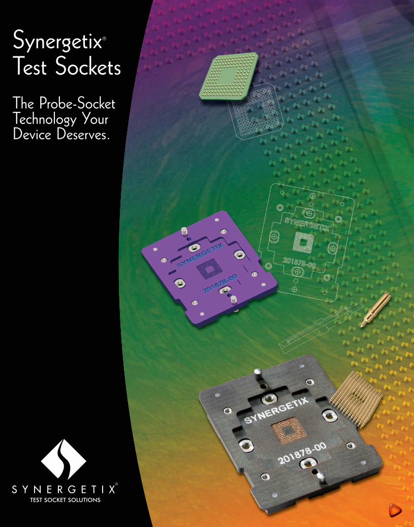
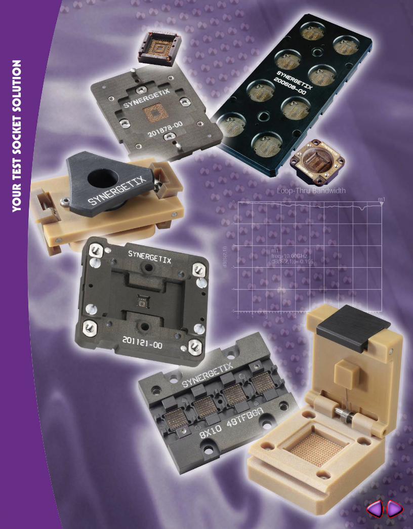
Synergetix®
Test SocketsThe Probe-SocketTechnology YourDevice Deserves.
YOUR PERFECT CONNECTIONTEST SOCKET SOLUTIONS
117aBinderCurved.qxd 8/4/2003 10:42 AM Page 1
YOUR
TES
T SO
CKET
SO
LUTI
ON
117aBinderCurved.qxd 8/4/2003 10:47 AM Page 2
TABLE O
F CON
TENTS
Table of ContentsSynergetix Test Socket Solutions
The Synergetix Advantage
Mechanical Performance Features
Electrical Performance Features
Synergetix History
Quality Control Capabilities
Customization Options
Contact Options
Socket Material Options
Heat Control Options
Lid Options
Probe Technology Versus Conventional Interconnect Options
Handler and DUT Board Options
Specialty Socket Options
SocketBuilder.com
Letter From the CEO
Probe Spec Sheets:
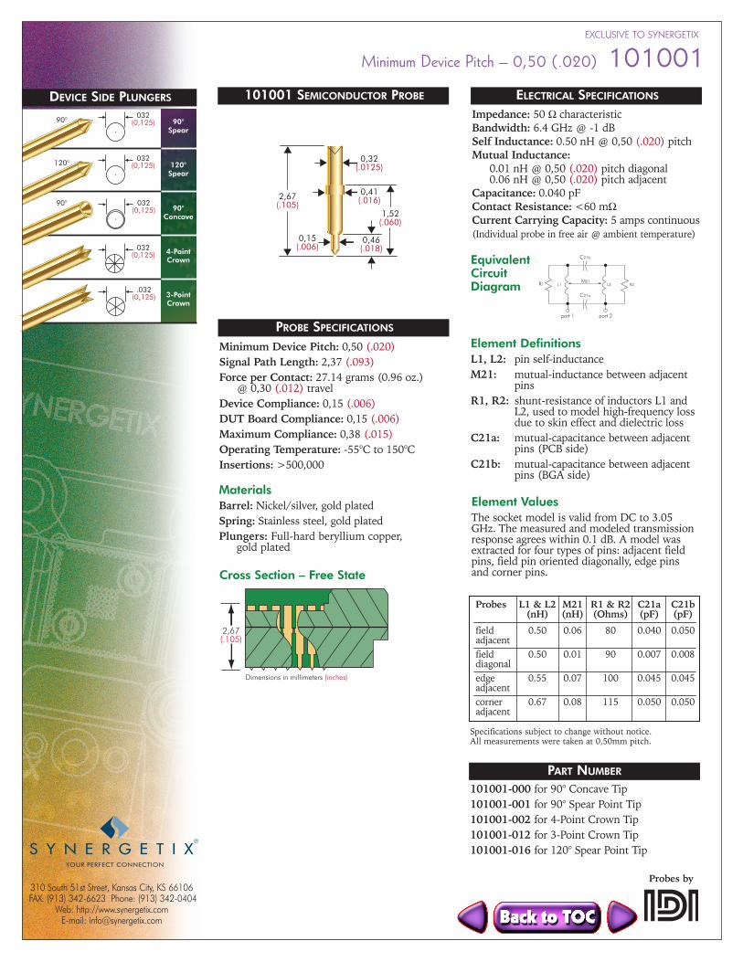
101001—Minimum Device Pitch: 0,50 (.020), Bandwidth: 6.4 GHz @ -1 dB
101041—Minimum Device Pitch: 0,50 (.020), Bandwidth: 6.4 GHz @ -1 dB
101210—Minimum Device Pitch: 0,50 (.020), Bandwidth: 4.5 GHz @ -1 dB
101085—Minimum Device Pitch: 0,65 (.026), Bandwidth: 7.8 GHz @ -1 dB
100938—Minimum Device Pitch: 0,65 (.026), Bandwidth: 2.4 GHz @ -1 dB
101052—Minimum Device Pitch: 0,75 (.029), Bandwidth: 10.0 GHz @ -1 dB
101053—Minimum Device Pitch: 0,75 (.029), Bandwidth: 10.0 GHz @ -1 dB
101111—Minimum Device Pitch: 0,75 (.029), Bandwidth: 10.0 GHz @ -1 dB
101084—Minimum Device Pitch: 0,75 (.029), Bandwidth: 6.3 GHz @ -1 dB
100881—Minimum Device Pitch: 1,00 (.039), Bandwidth: 2.9 GHz @ -1 dB
100929—Minimum Device Pitch: 1,00 (.039), Bandwidth: 2.0 GHz @ -1 dB
101150—Minimum Device Pitch: 1,27 (.050), Bandwidth: 10.0 GHz @ -1 dB
Socket Specifications
Request for Test Socket Quotation
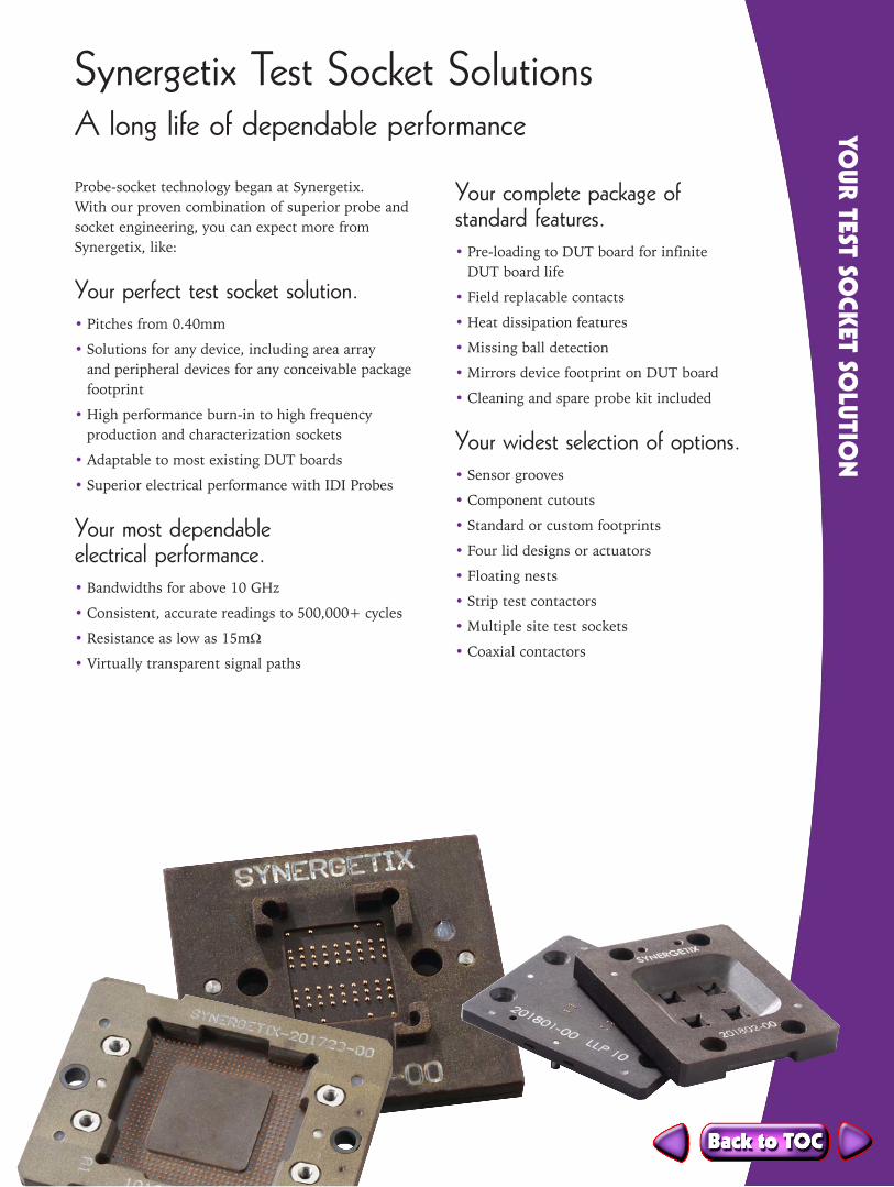
Your complete package of standard features.• Pre-loading to DUT board for infinite
DUT board life
• Field replacable contacts
• Heat dissipation features
• Missing ball detection
• Mirrors device footprint on DUT board
• Cleaning and spare probe kit included
Your widest selection of options.• Sensor grooves
• Component cutouts
• Standard or custom footprints
• Four lid designs or actuators
• Floating nests
• Strip test contactors
• Multiple site test sockets
• Coaxial contactors
Probe-socket technology began at Synergetix. With our proven combination of superior probe andsocket engineering, you can expect more fromSynergetix, like:
Your perfect test socket solution.• Pitches from 0.40mm
• Solutions for any device, including area array and peripheral devices for any conceivable packagefootprint
• High performance burn-in to high frequency production and characterization sockets
• Adaptable to most existing DUT boards
• Superior electrical performance with IDI Probes
Your most dependable electrical performance.• Bandwidths for above 10 GHz
• Consistent, accurate readings to 500,000+ cycles
• Resistance as low as 15mΩ
• Virtually transparent signal paths
Synergetix Test Socket SolutionsA long life of dependable performance YO
UR TEST SOCK
ET SOLUTIO
N
1
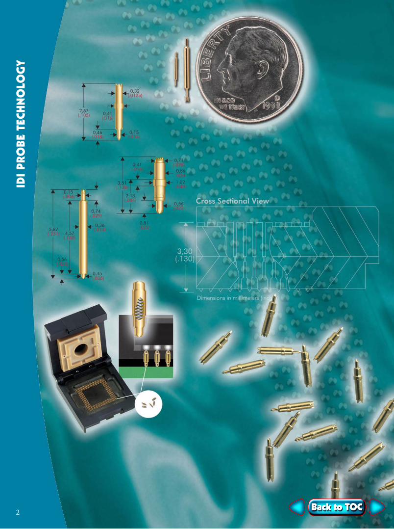
IDI
PRO
BE T
ECH
NO
LOG
Y
2
Electrical Performance Features:• Bandwidths for above 10 GHz
• Virtually transparent signal path for minimaldistortion
• Signal paths as short as 1.60mm
• Self-inductance as low as 0.33 nH
• Capacitance as low as .005 pF
• Operating temperature from -55°C to 150°C
• Current rating up to 6 amps
• 50 Ohm characteristic impedance
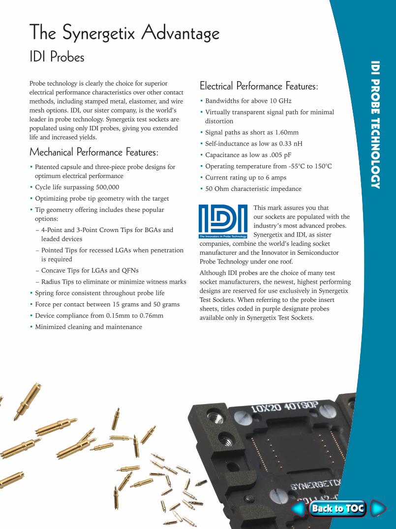
This mark assures you that our sockets are populated with theindustry’s most advanced probes.Synergetix and IDI, as sister
companies, combine the world’s leading socket manufacturer and the Innovator in SemiconductorProbe Technology under one roof.
Although IDI probes are the choice of many test socket manufacturers, the newest, highest performingdesigns are reserved for use exclusively in SynergetixTest Sockets. When referring to the probe insertsheets, titles coded in purple designate probes available only in Synergetix Test Sockets.
Probe technology is clearly the choice for superior electrical performance characteristics over other contactmethods, including stamped metal, elastomer, and wiremesh options. IDI, our sister company, is the world’sleader in probe technology. Synergetix test sockets arepopulated using only IDI probes, giving you extendedlife and increased yields.
Mechanical Performance Features:• Patented capsule and three-piece probe designs for
optimum electrical performance
• Cycle life surpassing 500,000
• Optimizing probe tip geometry with the target
• Tip geometry offering includes these popularoptions:
– 4-Point and 3-Point Crown Tips for BGAs andleaded devices
– Pointed Tips for recessed LGAs when penetrationis required
– Concave Tips for LGAs and QFNs
– Radius Tips to eliminate or minimize witness marks
• Spring force consistent throughout probe life
• Force per contact between 15 grams and 50 grams
• Device compliance from 0.15mm to 0.76mm
• Minimized cleaning and maintenance
The Synergetix AdvantageIDI Probes ID
I PROBE TECH
NO
LOG
Y
3

ABO
UT S
YNER
GET
IX
4
Quality Control CapabilitiesBefore we help you test, we test ourselves.Building sockets demands exact component toler-ances. In order to assure that these tolerances aremet, Synergetix assures the highest standards of accuracy throughout our quality control and failure analysis processes. All equipment used forinspection is calibrated and traceable to NISTstandards. Our capabilities include:
• ROI OMIS III 12x12 Automated VideoInspection Equipment
• Smart Scope 8x8x6 Automated VideoInspection Equipment
• X-ray examination
• HAST Testing
• Equipment+/- .0002" tolerance measurement
• Network Analyzer
• TDR — DC to 18 GHz
• LCR Meter
• Spice Modeling
early 1990’s, the company began a strategic initiative to identify new marketplaces where itscore competencies could be utilized competitively.Spring-loaded probes, after all, had proven them-selves to be ideal electro-mechanical connectors forPCB testing, why not introduce this technology toother applications where high reliability intercon-nect was demanded? The result of this initiative wasthe launch of Synergetix in 1994.
You know Synergetix for its leadership in the socketindustry. Yet our core competency in multi-cycle interconnection has been welcomed in other areaswhere reliability is critical. For example, we manufac-ture custom test interfaces for ATE manufacturers. We have also introduced probe technology to a broaderrange of markets. If you know an associate who isexploring new interconnect solutions please let themknow about Synergetix.
ABO
UT SYNERG
ETIX
5
Synergetix®
Where Probe-Socket Technology Began
When the first Synergetix Test Socket was delivered in1994, it was the result of a novel approach in socketmanufacturing. Never before had socket engineersdesigned side-by-side with probe engineers. This synergy of probe and socket engineering raised the barin socket performance standards to a whole new level.
When you talk to us, it doesn’t take long to realize that you’re teaming up with the leading probe-socketdevelopers. We ask questions that others don’t. Workingengineer-to-engineer, we understand what it takes todesign the best socket for your application. And we knowhow to choose the precise probe so your device alignsproperly in the socket for a 100% hit rate every time.
This excellence has earned us the socket business ofmany of the leaders in the semiconductor industry. InJapan, Synergetix is the leading brand of imported testsockets. We would like the opportunity to earn yoursocket business.
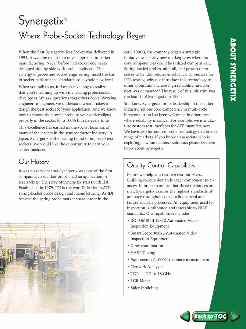
Our History It was no accident that Synergetix was one of the firstcompanies to see that probes had an application in test sockets. The story of Synergetix starts with IDI.Established in 1979, IDI is the world’s leader in ATEspring-loaded probe design and manufacturing. As IDIbecame the spring probe market share leader in the
Every chip is a unique creation and so is everysocket. Your Synergetix sales engineer anddesign engineer will help you determine whatoptions will be required for your SynergetixTest Socket.
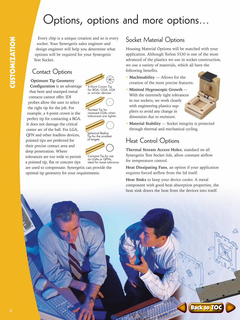
Contact OptionsOptimum Tip GeometryConfiguration is an advantagethat bent and stamped metalcontacts cannot offer. IDIprobes allow the user to selectthe right tip for the job. Forexample, a 4-point crown is theperfect tip for contacting a BGA.It does not damage the criticalcenter arc of the ball. For LGA,QFN and other leadless devices,pointed tips are preferred fortheir precise contact area anddeep penetration. Where tolerances are too wide to permita pointed tip, flat or concave tipsare used to compensate. Synergetix can provide theoptimal tip geometry for your requirements.
Socket Material OptionsHousing Material Options will be matched with yourapplication. Although Torlon 5530 is one of the mostadvanced of the plastics we use in socket construction,we use a variety of materials, which all have the following benefits.
• Machinability — Allows for the creation of the most precise features.
• Minimal Hygroscopic Growth —With the extremely tight tolerancesin our sockets, we work closelywith engineering plastics sup-pliers to avoid any change indimension due to moisture.
• Material Stability — Socket integrity is protectedthrough thermal and mechanical cycling.
Heat Control OptionsThermal Stream Access Holes, standard on allSynergetix Test Socket lids, allow constant airflow for temperature control.
Heat Dissipating Fans, an option if your applicationrequires forced airflow from the lid itself.
Heat Sinks to keep your device cooler. A metal component with good heat absorption properties, theheat sink draws the heat from the devices into itself.
Options, options and more options...CU
STO
MIZ
ATI
ON
6
Concave Tip for use on LGAs or QFNs, ideal for loose tolerance
Pointed Tip for recessed LGAs when tolerances are tighter
Spherical Radius Tip for the smallest of targets
4-Point Crown Tip for BGA, CGA, LGA or similar devices
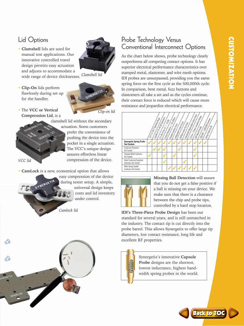
Lid Options• Clamshell lids are used for
manual test applications. Ourinnovative controlled traveldesign permits easy actuationand adjusts to accommodate awide range of device thicknesses.
• Clip-On lids performflawlessly during set upfor the handler.
• The VCC or VerticalCompression Lid, is a
clamshell lid without the secondaryactuation. Some customers
prefer the convenience ofpushing the device into thepocket in a single actuation.The VCC’s unique designassures effortless linearcompression of the device.
• CamLock is a new, economical option that allowseasy compression of the deviceduring tester setup. A simple,
universal design keepscosts and lid inventoryunder control.
Probe Technology Versus Conventional Interconnect Options As the chart below shows, probe technology clearlyoutperforms all competing contact options. It hassuperior electrical performance characteristics overstamped metal, elastomer, and wire mesh options. IDI probes are unsurpassed, providing you the samespring force on the first cycle as the 500,000th cycle. In comparison, bent metal, fuzz buttons and elastomers all take a set and as the cycles continue,their contact force is reduced which will cause moreresistance and jeopardize electrical performance.
Missing Ball Detection will assurethat you do not get a false positive if a ball is missing on your device. Wemake sure that there is a clearancebetween the chip and probe tips, controlled by a hard stop location.
IDI’s Three-Piece Probe Design has been our standard for several years, and is still unmatched in the industry. The contact tip is cut directly into theprobe barrel. This allows Synergetix to offer large tipdiameters, low contact resistance, long life and excellent RF properties.
CUSTOM
IZATIO
N
7
Synergetix Spring Probe Test Sockets
-55°
C to 1
50°C
Ope
ratin
g Ra
nge
Capa
ble of
.25
nH S
elf In
ducta
nce
0.5
dB of
Loss
@ >
10
GHz
Cont
act R
esist
ance
< 5
0 m
Ohm
s
Varia
ble In
serti
on Fo
rces
Inde
pend
ent C
onta
ct Fo
rces
Multip
le Co
ntac
t Tip
Style
sIn
dividu
ally R
eplac
eable
Cont
act P
oints
0,5m
m -
2,0m
m Co
mpli
ance
Ran
ge
DUT B
oard
Frien
dly50
0,00
0 - 1
,000
,000
Inse
rtion
s
Sprin
g Pr
obes
by I
DI
Conductive Elastomer Test Sockets
Stamped Metal Conductor Test Sockets
Metal Conductor/Compliant Elastomer Test Sockets
Other Spring Loaded Conductor Test Sockets
Camlock lid
Clip-on lid
Clamshell lid
VCC lid
Synergetix’s innovative CapsuleProbe designs are the shortest,lowest inductance, highest band-width spring probes in the world.
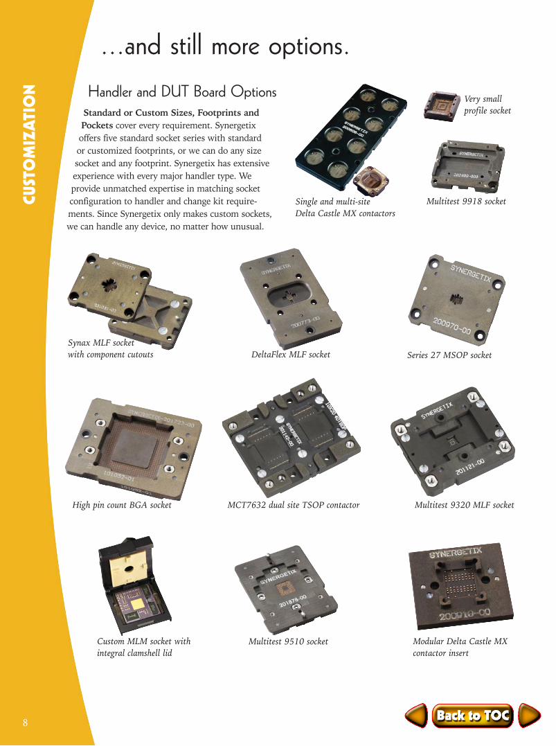
Handler and DUT Board OptionsStandard or Custom Sizes, Footprints andPockets cover every requirement. Synergetixoffers five standard socket series with standard or customized footprints, or we can do any sizesocket and any footprint. Synergetix has extensiveexperience with every major handler type. We provide unmatched expertise in matching socketconfiguration to handler and change kit require-ments. Since Synergetix only makes custom sockets,we can handle any device, no matter how unusual.
...and still more options.CU
STO
MIZ
ATI
ON
8
Multitest 9510 socket
DeltaFlex MLF socket Series 27 MSOP socket
Multitest 9918 socket
High pin count BGA socket
Custom MLM socket withintegral clamshell lid
Modular Delta Castle MXcontactor insert
Single and multi-site Delta Castle MX contactors
MCT7632 dual site TSOP contactor Multitest 9320 MLF socket
Synax MLF socket with component cutouts
Very smallprofile socket
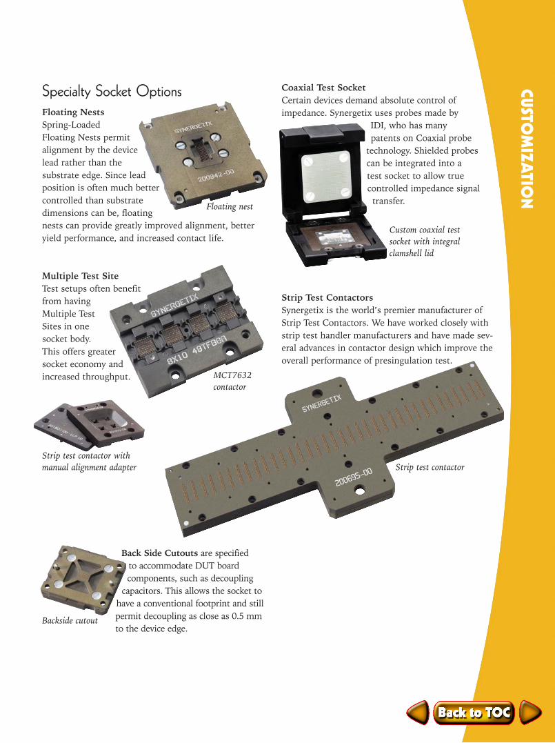
Back Side Cutouts are specified to accommodate DUT board components, such as decoupling
capacitors. This allows the socket tohave a conventional footprint and stillpermit decoupling as close as 0.5 mmto the device edge.
Strip Test ContactorsSynergetix is the world’s premier manufacturer ofStrip Test Contactors. We have worked closely withstrip test handler manufacturers and have made sev-eral advances in contactor design which improve theoverall performance of presingulation test.
Coaxial Test SocketCertain devices demand absolute control ofimpedance. Synergetix uses probes made by
IDI, who has manypatents on Coaxial probe
technology. Shielded probescan be integrated into a test socket to allow truecontrolled impedance signal
transfer.
CUSTOM
IZATIO
N
9
Specialty Socket OptionsFloating NestsSpring-LoadedFloating Nests permitalignment by the devicelead rather than the substrate edge. Since leadposition is often much bettercontrolled than substratedimensions can be, floatingnests can provide greatly improved alignment, betteryield performance, and increased contact life.
Multiple Test SiteTest setups often benefitfrom havingMultiple TestSites in one socket body. This offers greatersocket economy andincreased throughput.
Strip test contactor
Custom coaxial testsocket with integralclamshell lid
Floating nest
Strip test contactor withmanual alignment adapter
MCT7632contactor
Backside cutout
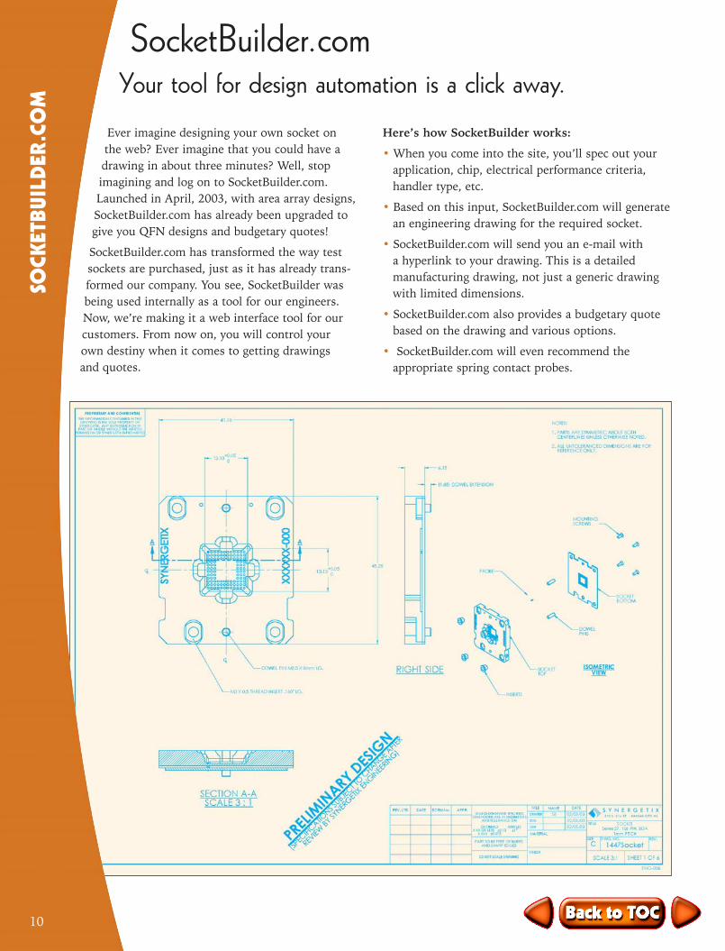
Ever imagine designing your own socket on the web? Ever imagine that you could have adrawing in about three minutes? Well, stopimagining and log on to SocketBuilder.com.Launched in April, 2003, with area array designs,SocketBuilder.com has already been upgraded togive you QFN designs and budgetary quotes!
SocketBuilder.com has transformed the way testsockets are purchased, just as it has already trans-formed our company. You see, SocketBuilder wasbeing used internally as a tool for our engineers.Now, we’re making it a web interface tool for ourcustomers. From now on, you will control your own destiny when it comes to getting drawings and quotes.
SocketBuilder.comYour tool for design automation is a click away.
SOCK
ETBU
ILD
ER.C
OM
10
Here’s how SocketBuilder works:
• When you come into the site, you’ll spec out yourapplication, chip, electrical performance criteria,handler type, etc.
• Based on this input, SocketBuilder.com will generatean engineering drawing for the required socket.
• SocketBuilder.com will send you an e-mail with a hyperlink to your drawing. This is a detailed manufacturing drawing, not just a generic drawingwith limited dimensions.
• SocketBuilder.com also provides a budgetary quotebased on the drawing and various options.
• SocketBuilder.com will even recommend the appropriate spring contact probes.

Use our flash animated
demo to see how easy it is
to use SocketBuilder.com
These are two sample
screens of the
SocketBuilder.com
automated design
application. In the screen
above, the user defines
the device footprint.
In the lower screen, the
user can customize the
socket footprint.
SOCK
ETBUILDER
.COM
11

We’ll Keep You Current...Dear Synergetix Test Socket Customer,
Synergetix has become an innovator of probe-socket technology, the
industry standard for ultimate performance. But we haven’t done this alone.
The innovations and impressive solutions you see in this brochure are the
result of thorough collaboration between our engineers and our customers.
But innovation has one drawback: it’s so easy for your literature to become
outdated! Hence, the reason for this pocket. We want to make sure the informa-
tion on the enclosed probe spec sheets represents the most current state of our
capabilities. When you refer to this folder in the future, please contact your sales
engineers for potential updates, or visit our web site at www.synergetix.com.
Another thing I’ve learned about innovation at Synergetix: it doesn’t stop with our test socket design and
manufacturing. Our award-winning web team has revolutionized the way we deliver our service. I am referring
to SocketBuilder.com, the unique web tool that has put socket design automation in the hands of our customers.
Imagine designing your own socket on the web. Now imagine that you could have a drawing in about three
minutes. That’s the reality of SocketBuilder.com! With this web innovation, what used to take us weeks is now
achieved by you in around three minutes.
I invite you to use SocketBuilder.com on your next test socket order. It will simplify your job and gain you
precious time. After you use it, let me know what you think by e-mailing me at [email protected].
Sincerely,
Ed Schifman
CEO, Synergetix
MES
SAG
E FR
OM
OUR
PRE
SID
ENT
12
YOUR PERFECT CONNECTION
310 South 51st Street, Kansas City, KS 66106 FAX: (913) 342-6623 Phone: (913) 342-0404
Web: http://www.synergetix.com E-mail: [email protected]
Probes by
90°Spear
120°Spear
90°Concave
4-PointCrown
3-PointCrown
.032(0,125)
032(0,125)90°
032(0,125)
90°
032(0,125)120°
032(0,125)
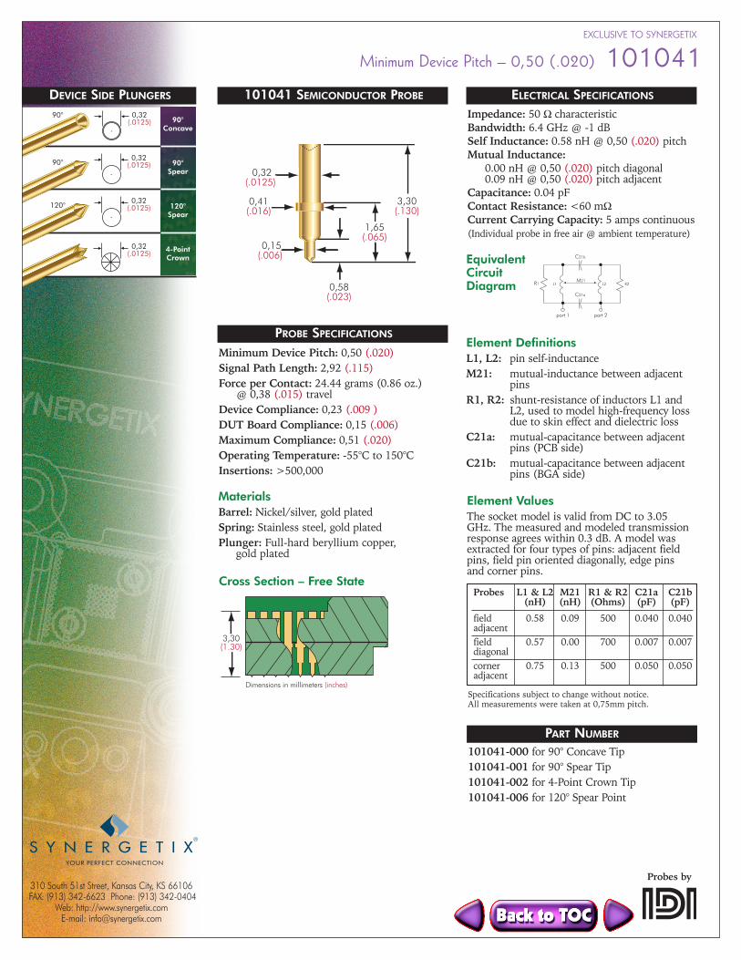
DEVICE SIDE PLUNGERS
Minimum Device Pitch – 0,50 (.020) 101001101001 SEMICONDUCTOR PROBE
0,41(.016)2,67
(.105)1,52 (.060)
0,15(.006)
0,32(.0125)
0,46(.018)
Minimum Device Pitch: 0,50 (.020)Signal Path Length: 2,37 (.093)Force per Contact: 27.14 grams (0.96 oz.)
@ 0,30 (.012) travelDevice Compliance: 0,15 (.006)DUT Board Compliance: 0,15 (.006)Maximum Compliance: 0,38 (.015)Operating Temperature: -55°C to 150°CInsertions: >500,000
PROBE SPECIFICATIONS
Impedance: 50 Ω characteristicBandwidth: 6.4 GHz @ -1 dBSelf Inductance: 0.50 nH @ 0,50 (.020) pitchMutual Inductance:
0.01 nH @ 0,50 (.020) pitch diagonal0.06 nH @ 0,50 (.020) pitch adjacent
Capacitance: 0.040 pFContact Resistance: <60 mΩCurrent Carrying Capacity: 5 amps continuous(Individual probe in free air @ ambient temperature)
ELECTRICAL SPECIFICATIONS
EquivalentCircuitDiagram
Element ValuesThe socket model is valid from DC to 3.05GHz. The measured and modeled transmissionresponse agrees within 0.1 dB. A model wasextracted for four types of pins: adjacent fieldpins, field pin oriented diagonally, edge pins and corner pins.
MaterialsBarrel: Nickel/silver, gold platedSpring: Stainless steel, gold platedPlungers: Full-hard beryllium copper,
gold plated
Element DefinitionsL1, L2: pin self-inductanceM21: mutual-inductance between adjacent
pinsR1, R2: shunt-resistance of inductors L1 and
L2, used to model high-frequency lossdue to skin effect and dielectric loss
C21a: mutual-capacitance between adjacentpins (PCB side)
C21b: mutual-capacitance between adjacentpins (BGA side)
R1 L1 L2 R2
port 1 port 2
M21
C21b
C21a
PART NUMBER
101001-000 for 90° Concave Tip101001-001 for 90° Spear Point Tip101001-002 for 4-Point Crown Tip101001-012 for 3-Point Crown Tip101001-016 for 120° Spear Point Tip
Cross Section – Free State
2,67(.105)
Dimensions in millimeters (inches)
Probes L1 & L2 M21 R1 & R2 C21a C21b(nH) (nH) (Ohms) (pF) (pF)
field 0.50 0.06 80 0.040 0.050adjacentfield 0.50 0.01 90 0.007 0.008diagonaledge 0.55 0.07 100 0.045 0.045adjacentcorner 0.67 0.08 115 0.050 0.050adjacent
Specifications subject to change without notice.All measurements were taken at 0,50mm pitch.
EXCLUSIVE TO SYNERGETIX
YOUR PERFECT CONNECTION
310 South 51st Street, Kansas City, KS 66106 FAX: (913) 342-6623 Phone: (913) 342-0404
Web: http://www.synergetix.com E-mail: [email protected]
Probes by
EXCLUSIVE TO SYNERGETIX
90°Concave
90°Spear
120°Spear
4-PointCrown
0,32(.0125)90°
0,32(.0125)
90°
0,32(.0125)120°
0,32(.0125)
DEVICE SIDE PLUNGERS
Minimum Device Pitch – 0,50 (.020) 101041101041 SEMICONDUCTOR PROBE
0,15(.006)
0,32(.0125)
0,41(.016)
3,30(.130)
0,58(.023)
1,65(.065)
Minimum Device Pitch: 0,50 (.020)Signal Path Length: 2,92 (.115)Force per Contact: 24.44 grams (0.86 oz.)
@ 0,38 (.015) travelDevice Compliance: 0,23 (.009 )DUT Board Compliance: 0,15 (.006)Maximum Compliance: 0,51 (.020)Operating Temperature: -55°C to 150°CInsertions: >500,000
PROBE SPECIFICATIONS
Impedance: 50 Ω characteristicBandwidth: 6.4 GHz @ -1 dBSelf Inductance: 0.58 nH @ 0,50 (.020) pitchMutual Inductance:
0.00 nH @ 0,50 (.020) pitch diagonal0.09 nH @ 0,50 (.020) pitch adjacent
Capacitance: 0.04 pFContact Resistance: <60 mΩCurrent Carrying Capacity: 5 amps continuous(Individual probe in free air @ ambient temperature)
ELECTRICAL SPECIFICATIONS
EquivalentCircuitDiagram
Element ValuesThe socket model is valid from DC to 3.05GHz. The measured and modeled transmissionresponse agrees within 0.3 dB. A model wasextracted for four types of pins: adjacent fieldpins, field pin oriented diagonally, edge pins and corner pins.
MaterialsBarrel: Nickel/silver, gold platedSpring: Stainless steel, gold platedPlunger: Full-hard beryllium copper,
gold plated
Element DefinitionsL1, L2: pin self-inductanceM21: mutual-inductance between adjacent
pinsR1, R2: shunt-resistance of inductors L1 and
L2, used to model high-frequency lossdue to skin effect and dielectric loss
C21a: mutual-capacitance between adjacentpins (PCB side)
C21b: mutual-capacitance between adjacentpins (BGA side)
Probes L1 & L2 M21 R1 & R2 C21a C21b(nH) (nH) (Ohms) (pF) (pF)
field 0.58 0.09 500 0.040 0.040adjacentfield 0.57 0.00 700 0.007 0.007diagonalcorner 0.75 0.13 500 0.050 0.050adjacent
Specifications subject to change without notice.All measurements were taken at 0,75mm pitch.
R1 L1 L2 R2
port 1 port 2
M21
C21b
C21a
PART NUMBER
101041-000 for 90° Concave Tip101041-001 for 90° Spear Tip101041-002 for 4-Point Crown Tip101041-006 for 120° Spear Point
Cross Section – Free State
3,30(1.30)
Dimensions in millimeters (inches)
YOUR PERFECT CONNECTION
310 South 51st Street, Kansas City, KS 66106 FAX: (913) 342-6623 Phone: (913) 342-0404
Web: http://www.synergetix.com E-mail: [email protected]
Probes by
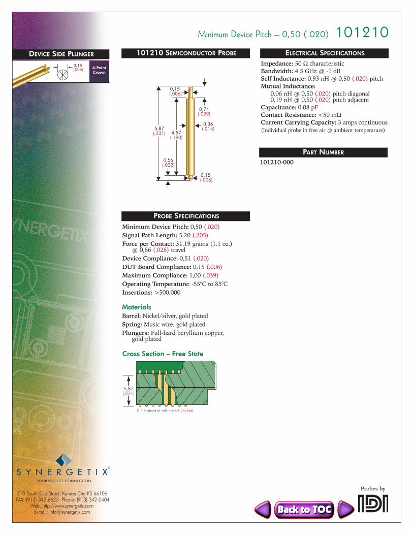
4-PointCrown
0,15(.006)
DEVICE SIDE PLUNGER
Minimum Device Pitch – 0,50 (.020) 101210101210 SEMICONDUCTOR PROBE
0,56 (.022)
0,15 (.006)
0,15 (.006)
0,36(.014)
0,74(.029)
4,57(.180)
5,87(.231)
Minimum Device Pitch: 0,50 (.020)Signal Path Length: 5,20 (.205)Force per Contact: 31.19 grams (1.1 oz.)
@ 0,66 (.026) travelDevice Compliance: 0,51 (.020)DUT Board Compliance: 0,15 (.006)Maximum Compliance: 1,00 (.039)Operating Temperature: -55°C to 85°CInsertions: >500,000
PROBE SPECIFICATIONS
Impedance: 50 Ω characteristicBandwidth: 4.5 GHz @ -1 dBSelf Inductance: 0.93 nH @ 0,50 (.020) pitchMutual Inductance:
0.06 nH @ 0,50 (.020) pitch diagonal0.19 nH @ 0,50 (.020) pitch adjacent
Capacitance: 0.08 pFContact Resistance: <50 mΩCurrent Carrying Capacity: 3 amps continuous(Individual probe in free air @ ambient temperature)
ELECTRICAL SPECIFICATIONS
MaterialsBarrel: Nickel/silver, gold platedSpring: Music wire, gold platedPlungers: Full-hard beryllium copper,
gold plated
PART NUMBER
101210-000
Cross Section – Free State
5,87(.231)
Dimensions in millimeters (inches)
YOUR PERFECT CONNECTION
310 South 51st Street, Kansas City, KS 66106 FAX: (913) 342-6623 Phone: (913) 342-0404
Web: http://www.synergetix.com E-mail: [email protected]
Probes by
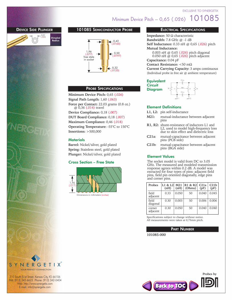
DimpledRadius
0,51(.020)
DEVICE SIDE PLUNGER
Minimum Device Pitch – 0,65 (.026) 101085101085 SEMICONDUCTOR PROBE
1,96(.077)
free state in socket
0,42(.0165)
0,32(.0125)
0,50(.0197)
Minimum Device Pitch: 0,65 (.026)Signal Path Length: 1,60 (.063)Force per Contact: 22.03 grams (0.8 oz.)
@ 0,36 (.014) travelDevice Compliance: 0,18 (.007)DUT Board Compliance: 0,18 (.007)Maximum Compliance: 0,46 (.018)Operating Temperature: -55°C to 150°CInsertions: >500,000
PROBE SPECIFICATIONS
Impedance: 50 Ω characteristicBandwidth: 7.8 GHz @ -1 dBSelf Inductance: 0.33 nH @ 0,65 (.026) pitchMutual Inductance:
0.003 nH @ 0,65 (.026) pitch diagonal0.050 nH @ 0,65 (.026) pitch adjacent
Capacitance: 0.04 pFContact Resistance: <50 mΩCurrent Carrying Capacity: 3 amps continuous(Individual probe in free air @ ambient temperature)
ELECTRICAL SPECIFICATIONS
EquivalentCircuitDiagram
Element ValuesThe socket model is valid from DC to 3.05GHz. The measured and modeled transmissionresponse agrees within 0.2 dB. A model wasextracted for four types of pins: adjacent fieldpins, field pin oriented diagonally, edge pins and corner pins.
MaterialsBarrel: Nickel/silver, gold platedSpring: Stainless steel, gold platedPlunger: Nickel/silver, gold plated
Element DefinitionsL1, L2: pin self-inductanceM21: mutual-inductance between adjacent
pinsR1, R2: shunt-resistance of inductors L1 and
L2, used to model high-frequency lossdue to skin effect and dielectric loss
C21a: mutual-capacitance between adjacentpins (PCB side)
C21b: mutual-capacitance between adjacentpins (BGA side)
Probes L1 & L2 M21 R1 & R2 C21a C21b(nH) (nH) (Ohms) (pF) (pF)
field 0.33 0.050 50 0.040 0.045adjacentfield 0.30 0.003 50 0.006 0.006diagonalcorner 0.30 0.050 50 0.040 0.040adjacent
Specifications subject to change without notice.All measurements were taken at 0,75mm pitch.
R1 L1 L2 R2
port 1 port 2
M21
C21b
C21a
PART NUMBER
101085-000
Cross Section – Free State
1,96(.077)
Dimensions in millimeters (inches)
EXCLUSIVE TO SYNERGETIX

YOUR PERFECT CONNECTION
310 South 51st Street, Kansas City, KS 66106 FAX: (913) 342-6623 Phone: (913) 342-0404
Web: http://www.synergetix.com E-mail: [email protected]
Probes by
60°Spear
SphericalRadius
4-PointCrown
0,25(.010)
0,25(.010)
60°
0,25(.010)
PLUNGER – BOTH ENDS 100938 SEMICONDUCTOR PROBE
0,25(.010)
5,72 (.225)
0,25(.010)
1,00 (.0395)
0,53(.021)
1,00(.0395)
Minimum Device Pitch: 0,65 (.026)Signal Path Length: 4,75 (.187)Force per Contact: 31.22 grams (1.1 oz.)
@ 0,97 (.038) travelDevice Compliance: 0,48 (.019)DUT Board Compliance: 0,48 (.019)Maximum Compliance: 1,30 (.051)Operating Temperature: -55°C to 150°CInsertions: >500,000
PROBE SPECIFICATIONS
Impedance: 50 Ω characteristicBandwidth: 2.4 GHz @ -1 dBSelf Inductance: 0.9 nH @ 0,75 (.029) pitchMutual Inductance:
0.09 nH @ 0,75 (.029) pitch diagonal0.23 nH @ 0,75 (.029) pitch adjacent
Capacitance: 0.10 pFContact Resistance: <70 mΩCurrent Carrying Capacity: 3 amps continuous(Individual probe in free air @ ambient temperature)
ELECTRICAL SPECIFICATIONS
EquivalentCircuitDiagram
Element ValuesThe socket model is valid from DC to 3.05GHz. The measured and modeled transmissionresponse agrees within 0.3 dB. A model wasextracted for four types of pins: adjacent fieldpins, field pin oriented diagonally, edge pins and corner pins.Materials
Barrel: Nickel/silver, gold platedSpring: Stainless steel, gold platedPlungers: Full-hard beryllium copper,
gold plated
Element DefinitionsL1, L2: pin self-inductanceM21: mutual-inductance between adjacent
pinsR1, R2: shunt-resistance of inductors L1 and
L2, used to model high-frequency lossdue to skin effect and dielectric loss
C21a: mutual-capacitance between adjacentpins (PCB side)
C21b: mutual-capacitance between adjacentpins (BGA side)
Probes L1 & L2 M21 R1 & R2 C21a C21b(nH) (nH) (Ohms) (pF) (pF)
field 0.9 0.23 250 0.10 0.10adjacentfield 0.9 0.09 250 0.04 0.04diagonaledge 1.0 0.30 250 0.14 0.14adjacentcorner 1.3 0.30 250 0.14 0.14adjacent
Specifications subject to change without notice.All measurements were taken at 0,75mm pitch.
R1 L1 L2 R2
port 1 port 2
M21
C21b
C21a
HOW TO ORDER
100938-001: for 4-point crown tip both ends100938-014: for 4-point crown tip and radius tip100938-015: for 4-point crown tip and spear tip100938-016: for radius tip both ends100938-018: for spear tip both ends
Cross Section – Free State
5,72(.225)
Dimensions in millimeters (inches)
Minimum Device Pitch – 0,65 (.026) 100938
YOUR PERFECT CONNECTION
310 South 51st Street, Kansas City, KS 66106 FAX: (913) 342-6623 Phone: (913) 342-0404
Web: http://www.synergetix.com E-mail: [email protected]
Probes by
4-PointCrown
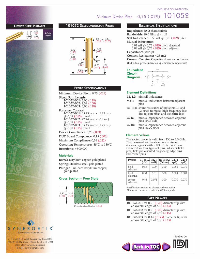
0,51(.020)
or0,44
(.0175)
DEVICE SIDE PLUNGER
Minimum Device Pitch – 0,75 (.029) 101052101052 SEMICONDUCTOR PROBE
2,92(.115)
or3,38(.133)
0,25(.010)
1,52(.060)
0,58(.023)
0,69(.027)
0,51(.020)
0,44(.0175)
0,25(.010)
or
Minimum Device Pitch: 0,75 (.029)Signal Path Length:
101052-001: 3,00 (.118)101052-002: 2,54 (.100)101052-003: 3,00 (.118)
Force per Contact:101052-001: 35.45 grams (1.25 oz.)@ 0,38 (.015) travel101052-002: 22.74 grams (0.8 oz.)@ 0,38 (.015) travel101052-003: 35.45 grams (1.25 oz.)@ 0,38 (.015) travel
Device Compliance: 0,23 (.009)DUT Board Compliance: 0,15 (.006)Maximum Compliance: 0,56 (.022)Operating Temperature: -55°C to 150°CInsertions: >500,000
PROBE SPECIFICATIONS
Impedance: 50 Ω characteristicBandwidth: 10.0 GHz @ -1 dBSelf Inductance: 0.56 nH @ 0,75 (.029) pitchMutual Inductance:
0.01 nH @ 0,75 (.029) pitch diagonal0.09 nH @ 0,75 (.029) pitch adjacent
Capacitance: 0.05 pFContact Resistance: <25 mΩCurrent Carrying Capacity: 6 amps continuous(Individual probe in free air @ ambient temperature)
ELECTRICAL SPECIFICATIONS
EquivalentCircuitDiagram
Element ValuesThe socket model is valid from DC to 3.0 GHz.The measured and modeled transmissionresponse agrees within 0.3 dB. A model wasextracted for four types of pins: adjacent fieldpins, field pin oriented diagonally, edge pins and corner pins.Materials
Barrel: Beryllium copper, gold platedSpring: Stainless steel, gold platedPlunger: Full-hard beryllium copper,
gold plated
Element DefinitionsL1, L2: pin self-inductanceM21: mutual-inductance between adjacent
pinsR1, R2: shunt-resistance of inductors L1 and
L2, used to model high-frequency lossdue to skin effect and dielectric loss
C21a: mutual-capacitance between adjacentpins (PCB side)
C21b: mutual-capacitance between adjacentpins (BGA side)
Probes L1 & L2 M21 R1 & R2 C21a C21b(nH) (nH) (Ohms) (pF) (pF)
field 0.56 0.09 300 0.055 0.070adjacentfield 0.54 0.01 300 0.009 0.008diagonalcorner 0.85 0.071 300 0.070 0.070adjacent
Specifications subject to change without notice.All measurements were taken at 0,75mm pitch.
R1 L1 L2 R2
port 1 port 2
M21
C21b
C21a
PART NUMBER
101052-001 for 0,51 (.020) diameter tip withan overall length of 3,38 (.133)
101052-002 for 0,51 (.020) diameter tip withan overall length of 2,92 (.115)
101052-003 for 0,44 (.0175) diameter tip withan overall length of 3,38 (.133)
Cross Section – Free State
3,38(.133)
2,92(.115)
Dimensions in millimeters (inches)
or
EXCLUSIVE TO SYNERGETIX
YOUR PERFECT CONNECTION
310 South 51st Street, Kansas City, KS 66106 FAX: (913) 342-6623 Phone: (913) 342-0404
Web: http://www.synergetix.com E-mail: [email protected]
Probes by
DEVICE SIDE PLUNGER
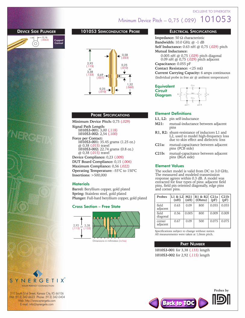
Minimum Device Pitch – 0,75 (.029) 101053101053 SEMICONDUCTOR PROBE
0,25(.010)
1,52(.060)
0,58(.023)
0,25(.010)
2,92(.115)
or3,38(.133) 0,69
(.027)
Minimum Device Pitch: 0,75 (.029)Signal Path Length:
101053-001: 3,00 (.118)101053-002: 2,54 (.100)
Force per Contact:101053-001: 35.45 grams (1.25 oz.)@ 0,38 (.015) travel101053-002: 22.74 grams (0.8 oz.)@ 0,38 (.015) travel
Device Compliance: 0,23 (.009)DUT Board Compliance: 0,15 (.006)Maximum Compliance: 0,56 (.022)Operating Temperature: -55°C to 150°CInsertions: >500,000
PROBE SPECIFICATIONS
MaterialsBarrel: Beryllium copper, gold platedSpring: Stainless steel, gold platedPlunger: Full-hard beryllium copper, gold plated
Cross Section – Free State
2,92(.115)
3,38(.133)
Dimensions in millimeters (inches)
or
Impedance: 50 Ω characteristicBandwidth: 10.0 GHz @ -1 dBSelf Inductance: 0.63 nH @ 0,75 (.029) pitchMutual Inductance:
0.005 nH @ 0,75 (.029) pitch diagonal0.09 nH @ 0,75 (.029) pitch adjacent
Capacitance: 0.055 pFContact Resistance: <25 mΩCurrent Carrying Capacity: 6 amps continuous(Individual probe in free air @ ambient temperature)
ELECTRICAL SPECIFICATIONS
EquivalentCircuitDiagram
Element ValuesThe socket model is valid from DC to 3.0 GHz.The measured and modeled transmissionresponse agrees within 0.3 dB. A model wasextracted for four types of pins: adjacent fieldpins, field pin oriented diagonally, edge pins and corner pins.
Element DefinitionsL1, L2: pin self-inductanceM21: mutual-inductance between adjacent
pinsR1, R2: shunt-resistance of inductors L1 and
L2, used to model high-frequency lossdue to skin effect and dielectric loss
C21a: mutual-capacitance between adjacentpins (PCB side)
C21b: mutual-capacitance between adjacentpins (BGA side)
Probes L1 & L2 M21 R1 & R2 C21a C21b(nH) (nH) (Ohms) (pF) (pF)
field 0.63 0.09 800 0.055 0.055adjacentfield 0.56 0.005 800 0.009 0.009diagonalcorner 0.67 0.09 500 0.075 0.075adjacent
Specifications subject to change without notice.All measurements were taken at 1,0mm pitch.
R1 L1 L2 R2
port 1 port 2
M21
C21b
C21a
PART NUMBER
101053-001 for 3,38 (.133) length101053-002 for 2,92 (.115) length
CuppedConical
0,16(.0063)
EXCLUSIVE TO SYNERGETIX
YOUR PERFECT CONNECTION
310 South 51st Street, Kansas City, KS 66106 FAX: (913) 342-6623 Phone: (913) 342-0404
Web: http://www.synergetix.com E-mail: [email protected]
Probes by
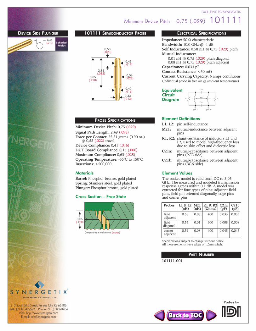
Minimum Device Pitch – 0,75 (.029) 101111EXCLUSIVE TO SYNERGETIX
101111 SEMICONDUCTOR PROBE
Minimum Device Pitch: 0,75 (.029)Signal Path Length: 2,49 (.098)Force per Contact: 25.51 grams (0.90 oz.)
@ 0,55 (.022) travelDevice Compliance: 0,41 (.016)DUT Board Compliance: 0,15 (.006)Maximum Compliance: 0,63 (.025)Operating Temperature: -55°C to 150°CInsertions: >500,000
PROBE SPECIFICATIONS
MaterialsBarrel: Phosphor bronze, gold platedSpring: Stainless steel, gold platedPlunger: Phosphor bronze, gold plated
Cross Section – Free State
3,05(.120)
Dimensions in millimeters (inches)
Impedance: 50 Ω characteristicBandwidth: 10.0 GHz @ -1 dBSelf Inductance: 0.58 nH @ 0,75 (.029) pitchMutual Inductance:
0.01 nH @ 0,75 (.029) pitch diagonal0.08 nH @ 0,75 (.029) pitch adjacent
Capacitance: 0.033 pFContact Resistance: <50 mΩCurrent Carrying Capacity: 6 amps continuous(Individual probe in free air @ ambient temperature)
ELECTRICAL SPECIFICATIONS
EquivalentCircuitDiagram
Element ValuesThe socket model is valid from DC to 3.05GHz. The measured and modeled transmissionresponse agrees within 0.1 dB. A model wasextracted for four types of pins: adjacent fieldpins, field pin oriented diagonally, edge pins and corner pins.
Element DefinitionsL1, L2: pin self-inductanceM21: mutual-inductance between adjacent
pinsR1, R2: shunt-resistance of inductors L1 and
L2, used to model high-frequency lossdue to skin effect and dielectric loss
C21a: mutual-capacitance between adjacentpins (PCB side)
C21b: mutual-capacitance between adjacentpins (BGA side)
Probes L1 & L2 M21 R1 & R2 C21a C21b(nH) (nH) (Ohms) (pF) (pF)
field 0.58 0.08 400 0.033 0.033adjacentfield 0.55 0.01 600 0.008 0.008diagonalcorner 0.59 0.08 400 0.045 0.045adjacent
Specifications subject to change without notice.All measurements were taken at 1,0mm pitch.
R1 L1 L2 R2
port 1 port 2
M21
C21b
C21a
PART NUMBER
101111-001
3,05(.120)
2,16(.085)
0,58 (.023)
0,43(.017)
0,40(.016)0,33(.013)
0,56(.022)
SphericalRadius
0,43(.017)
DEVICE SIDE PLUNGER
YOUR PERFECT CONNECTION
310 South 51st Street, Kansas City, KS 66106 FAX: (913) 342-6623 Phone: (913) 342-0404
Web: http://www.synergetix.com E-mail: [email protected]
Probes by
4-PointCrown
0,51(0,20)
DEVICE SIDE PLUNGER
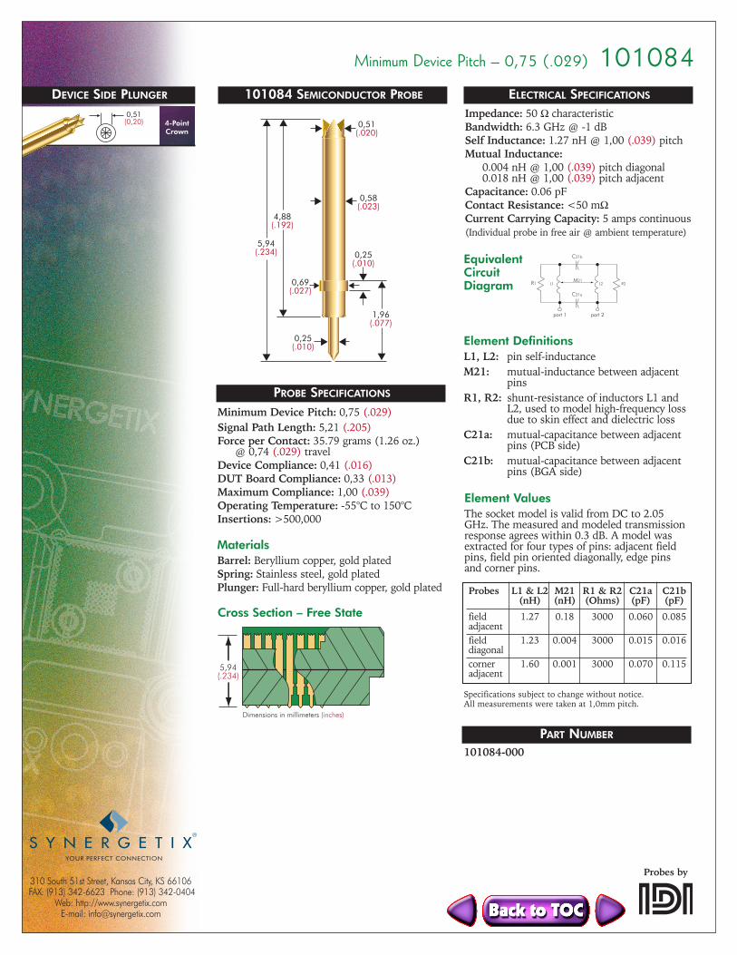
Minimum Device Pitch – 0,75 (.029) 101084
5,94(.234)
4,88(.192)
1,96(.077)
0,25(.010)
0,25(.010)
0,58(.023)
0,51(.020)
0,69(.027)
101084 SEMICONDUCTOR PROBE
Minimum Device Pitch: 0,75 (.029)Signal Path Length: 5,21 (.205)Force per Contact: 35.79 grams (1.26 oz.)
@ 0,74 (.029) travelDevice Compliance: 0,41 (.016)DUT Board Compliance: 0,33 (.013)Maximum Compliance: 1,00 (.039)Operating Temperature: -55°C to 150°CInsertions: >500,000
PROBE SPECIFICATIONS
MaterialsBarrel: Beryllium copper, gold platedSpring: Stainless steel, gold platedPlunger: Full-hard beryllium copper, gold plated
Cross Section – Free State
5,94(.234)
Dimensions in millimeters (inches)
Impedance: 50 Ω characteristicBandwidth: 6.3 GHz @ -1 dBSelf Inductance: 1.27 nH @ 1,00 (.039) pitchMutual Inductance:
0.004 nH @ 1,00 (.039) pitch diagonal0.018 nH @ 1,00 (.039) pitch adjacent
Capacitance: 0.06 pFContact Resistance: <50 mΩCurrent Carrying Capacity: 5 amps continuous(Individual probe in free air @ ambient temperature)
ELECTRICAL SPECIFICATIONS
EquivalentCircuitDiagram
Element ValuesThe socket model is valid from DC to 2.05GHz. The measured and modeled transmissionresponse agrees within 0.3 dB. A model wasextracted for four types of pins: adjacent fieldpins, field pin oriented diagonally, edge pins and corner pins.
Element DefinitionsL1, L2: pin self-inductanceM21: mutual-inductance between adjacent
pinsR1, R2: shunt-resistance of inductors L1 and
L2, used to model high-frequency lossdue to skin effect and dielectric loss
C21a: mutual-capacitance between adjacentpins (PCB side)
C21b: mutual-capacitance between adjacentpins (BGA side)
Probes L1 & L2 M21 R1 & R2 C21a C21b(nH) (nH) (Ohms) (pF) (pF)
field 1.27 0.18 3000 0.060 0.085adjacentfield 1.23 0.004 3000 0.015 0.016diagonalcorner 1.60 0.001 3000 0.070 0.115adjacent
Specifications subject to change without notice.All measurements were taken at 1,0mm pitch.
R1 L1 L2 R2
port 1 port 2
M21
C21b
C21a
PART NUMBER
101084-000
YOUR PERFECT CONNECTION
310 South 51st Street, Kansas City, KS 66106 FAX: (913) 342-6623 Phone: (913) 342-0404
Web: http://www.synergetix.com E-mail: [email protected]
Probes by
4-PointCrown
0,76(.030)
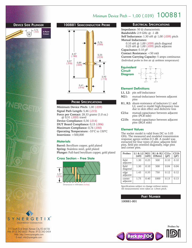
DEVICE SIDE PLUNGER 100881 SEMICONDUCTOR PROBE
0,25(.010)
2,92(.115)
0,76(.030)
0,41(.016)
5,97(.235)
4,57(.180)
0,89(.035)
Minimum Device Pitch: 1,00 (.039)Signal Path Length: 5,46 (.215)Force per Contact: 28.33 grams (1.0 oz.)
@ 0,51 (.020) travelDevice Compliance: 0,36 (.014)DUT Board Compliance: 0,15 (.006)Maximum Compliance: 0,76 (.030)Operating Temperature: -55°C to 150°CInsertions: >500,000
PROBE SPECIFICATIONS
MaterialsBarrel: Beryllium copper, gold platedSpring: Stainless steel, gold platedPlunger: Full-hard beryllium copper, gold plated
Cross Section – Free State
5,97(.235)
Dimensions in millimeters (inches)
Minimum Device Pitch – 1,00 (.039) 100881
Impedance: 50 Ω characteristicBandwidth: 2.9 GHz @ -1 dBSelf Inductance: 1.30 nH @ 1,00 (.039) pitchMutual Inductance:
0.10 nH @ 1,00 (.039) pitch diagonal0.25 nH @ 1,00 (.039) pitch adjacent
Capacitance: 0.10 pFContact Resistance: <50 mΩCurrent Carrying Capacity: 5 amps continuous(Individual probe in free air @ ambient temperature)
ELECTRICAL SPECIFICATIONS
EquivalentCircuitDiagram
Element ValuesThe socket model is valid from DC to 3.05GHz. The measured and modeled transmissionresponse agrees within 0.3 dB. A model wasextracted for four types of pins: adjacent fieldpins, field pin oriented diagonally, edge pins and corner pins.
Element DefinitionsL1, L2: pin self-inductanceM21: mutual-inductance between adjacent
pinsR1, R2: shunt-resistance of inductors L1 and
L2, used to model high-frequency lossdue to skin effect and dielectric loss
C21a: mutual-capacitance between adjacentpins (PCB side)
C21b: mutual-capacitance between adjacentpins (BGA side)
Probes L1 & L2 M21 R1 & R2 C21a C21b(nH) (nH) (Ohms) (pF) (pF)
field 1.30 0.25 500 0.10 0.10adjacentfield 1.30 0.10 500 0.04 0.04diagonaledge 1.45 0.35 750 0.12 0.12adjacentcorner 1.75 0.40 1000 0.13 0.13adjacent
Specifications subject to change without notice.All measurements were taken at 1,0mm pitch.
R1 L1 L2 R2
port 1 port 2
M21
C21b
C21a
PART NUMBER
100881-001
YOUR PERFECT CONNECTION
310 South 51st Street, Kansas City, KS 66106 FAX: (913) 342-6623 Phone: (913) 342-0404
Web: http://www.synergetix.com E-mail: [email protected]
Probes by
4-PointCrown
0,76(.030)
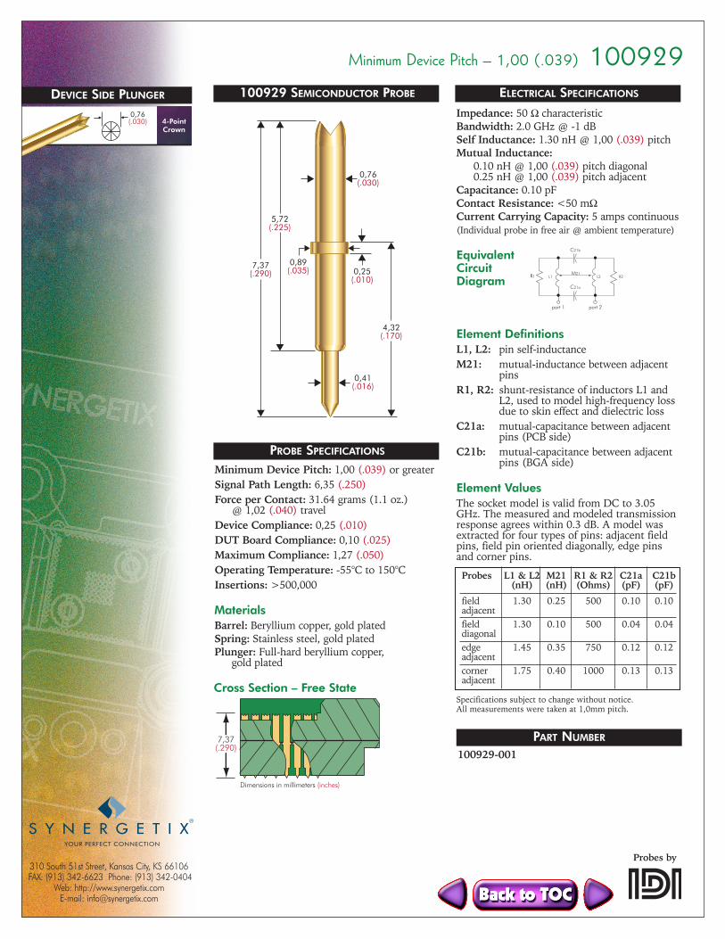
DEVICE SIDE PLUNGER 100929 SEMICONDUCTOR PROBE
7,37(.290)
5,72(.225)
0,25(.010)
4,32(.170)
0,76(.030)
0,89(.035)
0,41(.016)
Minimum Device Pitch: 1,00 (.039) or greaterSignal Path Length: 6,35 (.250)Force per Contact: 31.64 grams (1.1 oz.)
@ 1,02 (.040) travelDevice Compliance: 0,25 (.010)DUT Board Compliance: 0,10 (.025)Maximum Compliance: 1,27 (.050)Operating Temperature: -55°C to 150°CInsertions: >500,000
PROBE SPECIFICATIONS
Impedance: 50 Ω characteristicBandwidth: 2.0 GHz @ -1 dBSelf Inductance: 1.30 nH @ 1,00 (.039) pitchMutual Inductance:
0.10 nH @ 1,00 (.039) pitch diagonal0.25 nH @ 1,00 (.039) pitch adjacent
Capacitance: 0.10 pFContact Resistance: <50 mΩCurrent Carrying Capacity: 5 amps continuous(Individual probe in free air @ ambient temperature)
EquivalentCircuitDiagram
Element ValuesThe socket model is valid from DC to 3.05GHz. The measured and modeled transmissionresponse agrees within 0.3 dB. A model wasextracted for four types of pins: adjacent fieldpins, field pin oriented diagonally, edge pins and corner pins.
MaterialsBarrel: Beryllium copper, gold platedSpring: Stainless steel, gold platedPlunger: Full-hard beryllium copper,
gold plated
Element DefinitionsL1, L2: pin self-inductanceM21: mutual-inductance between adjacent
pinsR1, R2: shunt-resistance of inductors L1 and
L2, used to model high-frequency lossdue to skin effect and dielectric loss
C21a: mutual-capacitance between adjacentpins (PCB side)
C21b: mutual-capacitance between adjacentpins (BGA side)
Probes L1 & L2 M21 R1 & R2 C21a C21b(nH) (nH) (Ohms) (pF) (pF)
field 1.30 0.25 500 0.10 0.10adjacentfield 1.30 0.10 500 0.04 0.04diagonaledge 1.45 0.35 750 0.12 0.12adjacentcorner 1.75 0.40 1000 0.13 0.13adjacent
Specifications subject to change without notice.All measurements were taken at 1,0mm pitch.
R1 L1 L2 R2
port 1 port 2
M21
C21b
C21a
PART NUMBER
100929-001
Minimum Device Pitch – 1,00 (.039) 100929
Cross Section – Free State
7,37(.290)
Dimensions in millimeters (inches)
ELECTRICAL SPECIFICATIONS
YOUR PERFECT CONNECTION
310 South 51st Street, Kansas City, KS 66106 FAX: (913) 342-6623 Phone: (913) 342-0404
Web: http://www.synergetix.com E-mail: [email protected]
Probes by
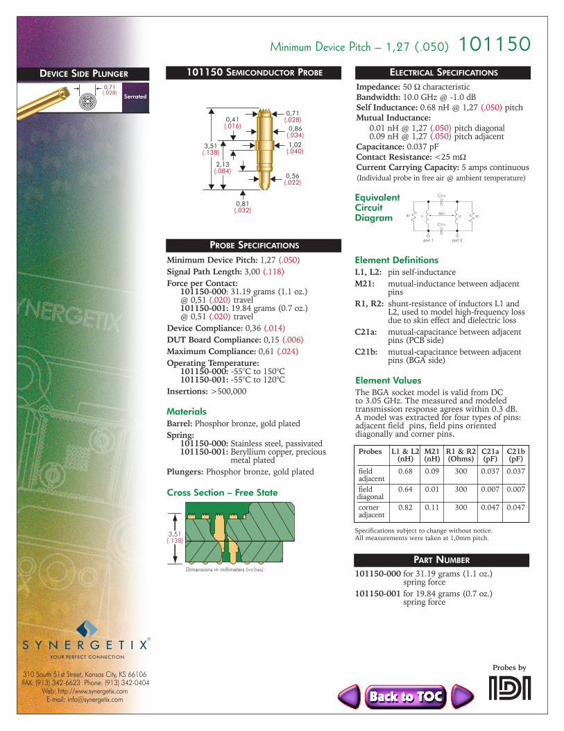
Serrated
0,71(.028)
DEVICE SIDE PLUNGER
Minimum Device Pitch – 1,27 (.050) 101150101150 SEMICONDUCTOR PROBE
1,02(.040)
0,86(.034)
0,71(.028)
0,56(.022)
0,81(.032)
0,41(.016)
2,13(.084)
3,51(.138)
Minimum Device Pitch: 1,27 (.050)Signal Path Length: 3,00 (.118)Force per Contact:
101150-000: 31.19 grams (1.1 oz.)@ 0,51 (.020) travel101150-001: 19.84 grams (0.7 oz.)@ 0,51 (.020) travel
Device Compliance: 0,36 (.014)DUT Board Compliance: 0,15 (.006)Maximum Compliance: 0,61 (.024)Operating Temperature:
101150-000: -55°C to 150°C101150-001: -55°C to 120°C
Insertions: >500,000
PROBE SPECIFICATIONS
Impedance: 50 Ω characteristicBandwidth: 10.0 GHz @ -1.0 dBSelf Inductance: 0.68 nH @ 1,27 (.050) pitchMutual Inductance:
0.01 nH @ 1,27 (.050) pitch diagonal0.09 nH @ 1,27 (.050) pitch adjacent
Capacitance: 0.037 pFContact Resistance: <25 mΩCurrent Carrying Capacity: 5 amps continuous(Individual probe in free air @ ambient temperature)
ELECTRICAL SPECIFICATIONS
PART NUMBER
101150-000 for 31.19 grams (1.1 oz.)spring force
101150-001 for 19.84 grams (0.7 oz.)spring force
3,51(.138)
Dimensions in millimeters (inches)
MaterialsBarrel: Phosphor bronze, gold platedSpring:
101150-000: Stainless steel, passivated101150-001: Beryllium copper, precious
metal platedPlungers: Phosphor bronze, gold plated
Cross Section – Free State
EquivalentCircuitDiagram
Element ValuesThe BGA socket model is valid from DC to 3.05 GHz. The measured and modeledtransmission response agrees within 0.3 dB. A model was extracted for four types of pins:adjacent field pins, field pins oriented diagonally and corner pins.
Element DefinitionsL1, L2: pin self-inductanceM21: mutual-inductance between adjacent
pinsR1, R2: shunt-resistance of inductors L1 and
L2, used to model high-frequency lossdue to skin effect and dielectric loss
C21a: mutual-capacitance between adjacentpins (PCB side)
C21b: mutual-capacitance between adjacentpins (BGA side)
Probes L1 & L2 M21 R1 & R2 C21a C21b(nH) (nH) (Ohms) (pF) (pF)
field 0.68 0.09 300 0.037 0.037adjacentfield 0.64 0.01 300 0.007 0.007diagonalcorner 0.82 0.11 300 0.047 0.047adjacent
Specifications subject to change without notice.All measurements were taken at 1,0mm pitch.
R1 L1 L2 R2
port 1 port 2
M21
C21b
C21a
YOUR PERFECT CONNECTION
310 South 51st Street, Kansas City, KS 66106 FAX: (913) 342-6623 Phone: (913) 342-0404
Web: http://www.synergetix.com E-mail: [email protected]
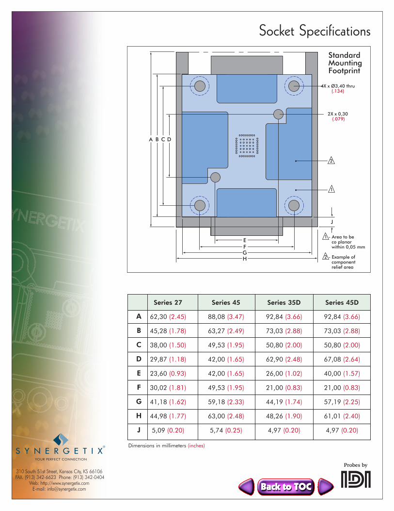
Socket Specifications
Probes by
1 - Area to be co planar within 0,05 mm
2 - Example of component relief area
1
2
A B C D
E
J
FGH
4X x Ø3,40 thru (.134)
2X x 0,30 (.079)
Series 27 Series 45 Series 35D Series 45D
62,30 (2.45) 88,08 (3.47) 92,84 (3.66) 92,84 (3.66)
45,28 (1.78) 63,27 (2.49) 73,03 (2.88) 73,03 (2.88)
38,00 (1.50) 49,53 (1.95) 50,80 (2.00) 50,80 (2.00)
29,87 (1.18) 42,00 (1.65) 62,90 (2.48) 67,08 (2.64)
23,60 (0.93) 42,00 (1.65) 26,00 (1.02) 40,00 (1.57)
30,02 (1.81) 49,53 (1.95) 21,00 (0.83) 21,00 (0.83)
41,18 (1.62) 59,18 (2.33) 44,19 (1.74) 57,19 (2.25)
44,98 (1.77) 63,00 (2.48) 48,26 (1.90) 61,01 (2.40)
5,09 (0.20) 5,74 (0.25) 4,97 (0.20) 4,97 (0.20)
A
B
C
D
E
F
G
H
J
Dimensions in millimeters (inches)
StandardMountingFootprint

YOUR PERFECT CONNECTION
310 South 51st Street, Kansas City, KS 66106 FAX: (913) 342-6623 Phone: (913) 342-0404
Web: http://www.synergetix.com E-mail: [email protected]
Request for Test Socket QuotationLid RequirementsStyle
ClamshellControlled Travel – Star Handle
Bolt-on Slide-onFree Travel – 3 Lobe Handle
Bolt-on Slide-on Clip-on Integral VCC Clip-on One Piece Bolt-Down
FeaturesIs heat dissipation required? Yes No
If yes, how much? <20 Watts 20-35 Watts >35 Watts
Application Used with handler Hand test
If a handler is used, what type? ____________Is this a new application? Yes ExistingOther requirements: _________________________
Quantity Requested ship date:Socket
Prototype: _____ ______________________Production: ____ ______________________
LidPrototype: _____ ______________________Production: ____ ______________________
Additional comments:__________________________________________________________________________________________________________________________________________________________________________________________________________________________________________________________________________________________________________________________________________________________________________________________________________________________________________________________________
Please fax your Request for Quotation to (913) 342-6623. Thank you.
Date: _______________________________________Name:_______________________________________Title: _______________________________________Company: ___________________________________Address: ____________________________________City: ________________________________________State: ___________ Zip Code: _________________Country: ____________________________________Phone: ________________________ X____________Fax: ___________________________E-MAIL: _____________________________________
Device RequirementsDevice Family:
BGA PGA Leaded Leadless Other
Please submit complete device drawings (includingdimensions and tolerances)
If device drawings not available, please fill out the below:Array pitch: _________________________________
Number of balls, lands, leads, etc.: _____________
Size of contacts (balls, lands, leads, etc.): _______
Number of probes for Ground Pad (if applicable): Minimum Nominal Maximum (heat dissipation)
Socket PreferencesNumber of sites: Single Multiple
If multiple, how many? ___________________Are component relief cutouts required? Yes No
If yes, please specify:______________________Are specific board fasteners required? Yes No
If yes, please specify:______________________Are specific alignment dowels required?
Yes No If yes, please specify:______________________
Is custom engraving required? Yes NoIf yes, please specify:______________________
Temperature RequirementsMax. temp: __________°C Duration: ___________Min. temp: __________°C Duration: ___________
Electrical RequirementsMax. operating frequency (in GHz): ____________Max. current (in amps): _____
Constant IntermittentIf intermittent, the cycle time on/off: _________________________________________
Other electrical parameters:_________________________________________________________________


![TEE Sockets API Specification v1.0 - GlobalPlatform · TEE Sockets API Specification Annex A: TCP/IP Specification of TEE Sockets API Specification [Sockets TCP/IP] GPD_SPE_102 :](https://img.pdfslide.net/doc/110x75/60421070f2b21560856dea9a/tee-sockets-api-specification-v10-globalplatform-tee-sockets-api-specification.jpg)