Embed Size (px)
Citation preview

SYNOPSIS
ON
AUTOMATIC RAILWAY CROSSING SYSTEM
Submitted in partial fulfillment of the requirement forThe award of degree
of B.TECH IN MECHANICAL ENGINEERING
Submitted by:- Guided by:-
Anuj Tyagi (3408419) Er. Goutam AroraArun Kumar (3408420) (Project Guide)Pawan Jeet (3408421) Mohit Kumar (3408422)Chirag Arora (3408423)Sandeep Kumar (3408424)
Department of Mechanical EngineeringS.D. Institute of Technology & Management
Israna-(Panipat)

ABSTRACT
Present project is designed using 8051 microcontroller to avoid
railway accidents happening at unattended railway gates, if
implemented in spirit. This project utilizes two powerful IR
transmitters and two receivers; one pair of transmitter and receiver is
fixed at up side (from where the train comes) at a level higher than a
human being in exact alignment and similarly the other pair is fixed
at down side of the train direction. Sensor activation time is so
adjusted by calculating the time taken at a certain speed to cross at
least one compartment of standard minimum size of the Indian
railway. We have considered 5 seconds for this project. Sensors are
fixed at 1km on both sides of the gate. We call the sensor along the
train direction as ‘foreside sensor’ and the other as ‘aft side sensor’.
When foreside receiver gets activated, the gate motor is turned on in
one direction and the gate is closed and stays closed until the train
crosses the gate and reaches aft side sensors. When aft side receiver
gets activated motor turns in opposite direction and gate opens and
motor stops. Buzzer will immediately sound at the fore side receiver
activation and gate will close after 5 seconds, so giving time to
drivers to clear gate area in order to avoid trapping between the
gates and stop sound after the train has crossed.
The same principle is applied for track switching. Considering a
situation wherein an express train and a local train are traveling in
opposite directions on the same track; the express train is allowed to

travel on the same track and the local train has to switch on to the
other track. Two sensors are placed at the either sides of the junction
where the track switches. If there’s a train approaching from the
other side, then another sensor placed along that direction gets
activated and will send an interrupt to the controller. The interrupt
service routine switches the track. Indicator lights have been
provided to avoid collisions. Here the switching operation is
performed using a stepper motor. Assuming that within a certain
delay, the train has passed the track is switched back to its original
position, allowing the first train to pass without any interruption. This
concept of track switching can be applied at 1km distance from the
stations.
The project is simple to implement and subject to further
improvement.

Model of Automatic Railway Gate Control & Track Switching
Railways being the cheapest mode of transportation are preferred
over all the other means .When we go through the daily newspapers
we come across many railway accidents occurring at unmanned
railway crossings. This is mainly due to the carelessness in manual
operations or lack of workers. We, in this project has come up with a
solution for the same. Using simple electronic components we have
tried to automate the control of railway gates. As a train approaches
the railway crossing from either side, the sensors placed at a certain
distance from the gate detects the approaching train and accordingly
controls the operation of the gate. Also an indicator light has been
provided to alert the motorists about the approaching train.

Gate controlTrack Switching
Using the same principle as that for gate control, we have developed
a concept of automatic track switching. Considering a situation
wherein an express train and a local train are traveling in opposite
directions on the same track; the express train is allowed to travel on
the same track and the local train has to switch on to the other track.
Indicator lights have been provided to avoid collisions .Here the
switching operation is performed using a stepper motor. In practical
purposes this can be achieved using electromagnets.

INTRODUCTION TO MICROCONTROLLERS
A micro-controller can be compared to a small stand alone computer, it is a
very powerful device, which is capable of executing a series of pre-
programmed tasks and interacting with other hardware devices. Being
packed in a tiny integrated circuit (IC) whose size and weight is usually
negligible, it is becoming the perfect controller for robots or any machines
requiring some kind of intelligent automation. A single microcontroller can
be sufficient to control a small mobile robot, an automatic washer machine
or a security system. Any microcontroller contains a memory to store the
program to be executed, and a number of input/output lines that can be used
to interact with other devices, like reading the state of a sensor or controlling
a motor.
Nowadays, microcontrollers are so cheap and easily available that it is
common to use them instead of simple logic circuits like counters for the
sole purpose of gaining some design flexibility and saving some space.
Some machines and robots will even rely on a multitude of microcontrollers,
each one dedicated to a certain task.
Today, microcontrollers are an indispensable tool for the robotics hobbyist
as well as for the engineer. Starting in this field can be a little difficult,
because you usually can't understand how everything works inside that
integrated circuit, so you have to study the system gradually, a small part at
a time, until you can figure out the whole image and understand how the
system works.

The underlying principle mainly relies up on the ability
of DTMF (Double Tune Multi Frequency) ICs to generate DTMF
corresponding to a number or code in the number pad and to detect
the same number or code from its corresponding DTMF. In detail, a
DTMF generator generates two frequencies corresponding to a
number or code in the number pad which will be transmitted through
the communication networks, constituting the transmitter section
which is simply equivalent to a mobile set. In the receiver part, the
DTMF detector IC, for example IC MT 8870 detects the number or
code represented by DTMF back, through the inspection of the two
transmitted frequencies. The DTMF frequencies representing the
number/ codes are shown below.
The 8051 microcontroller architecture
The 8051 is the name of a big family of microcontrollers. The device which
we are going to use along this report is the 'AT89S52' which is a typical 8051
microcontroller manufactured by Atmel™. Note that this part doesn't aim to
explain the functioning of the different components of a 89S52
microcontroller, but rather to give you a general idea of the organization of
the chip and the available features, which shall be explained in detail along
this report.
The block diagram provided by Atmel™ in their datasheet showing the
architecture the 89S52 device can seem very complicated, and since we are
going to use the its own assembly language to program it, a simpler
architecture can be represented as the figure 1.2.A.
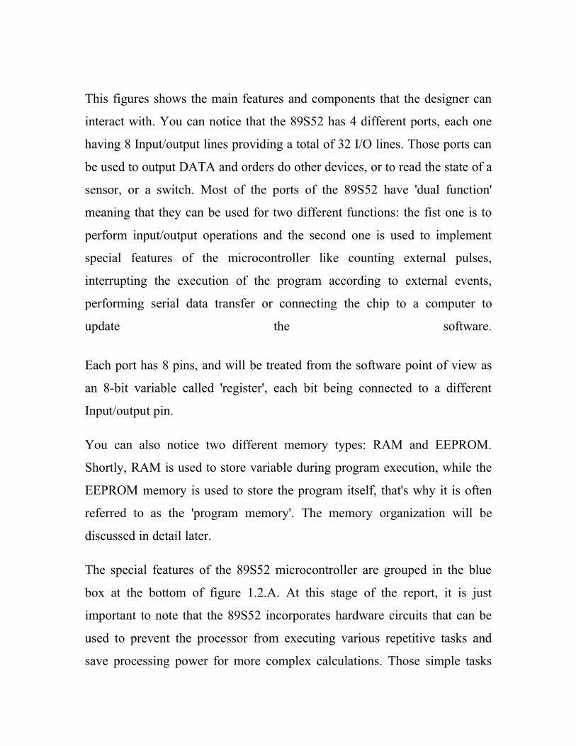
This figures shows the main features and components that the designer can
interact with. You can notice that the 89S52 has 4 different ports, each one
having 8 Input/output lines providing a total of 32 I/O lines. Those ports can
be used to output DATA and orders do other devices, or to read the state of a
sensor, or a switch. Most of the ports of the 89S52 have 'dual function'
meaning that they can be used for two different functions: the fist one is to
perform input/output operations and the second one is used to implement
special features of the microcontroller like counting external pulses,
interrupting the execution of the program according to external events,
performing serial data transfer or connecting the chip to a computer to
update the software.
Each port has 8 pins, and will be treated from the software point of view as
an 8-bit variable called 'register', each bit being connected to a different
Input/output pin.
You can also notice two different memory types: RAM and EEPROM.
Shortly, RAM is used to store variable during program execution, while the
EEPROM memory is used to store the program itself, that's why it is often
referred to as the 'program memory'. The memory organization will be
discussed in detail later.
The special features of the 89S52 microcontroller are grouped in the blue
box at the bottom of figure 1.2.A. At this stage of the report, it is just
important to note that the 89S52 incorporates hardware circuits that can be
used to prevent the processor from executing various repetitive tasks and
save processing power for more complex calculations. Those simple tasks

can be counting the number of external pulses on a pin, or generating precise
timing sequences.
Fig 1.2.A
It is clear that the CPU (Central Processing Unit) is the heart of the
microcontroller, It is the CPU that will Read the program from the FLASH
memory and execute it by interacting with the different peripherals
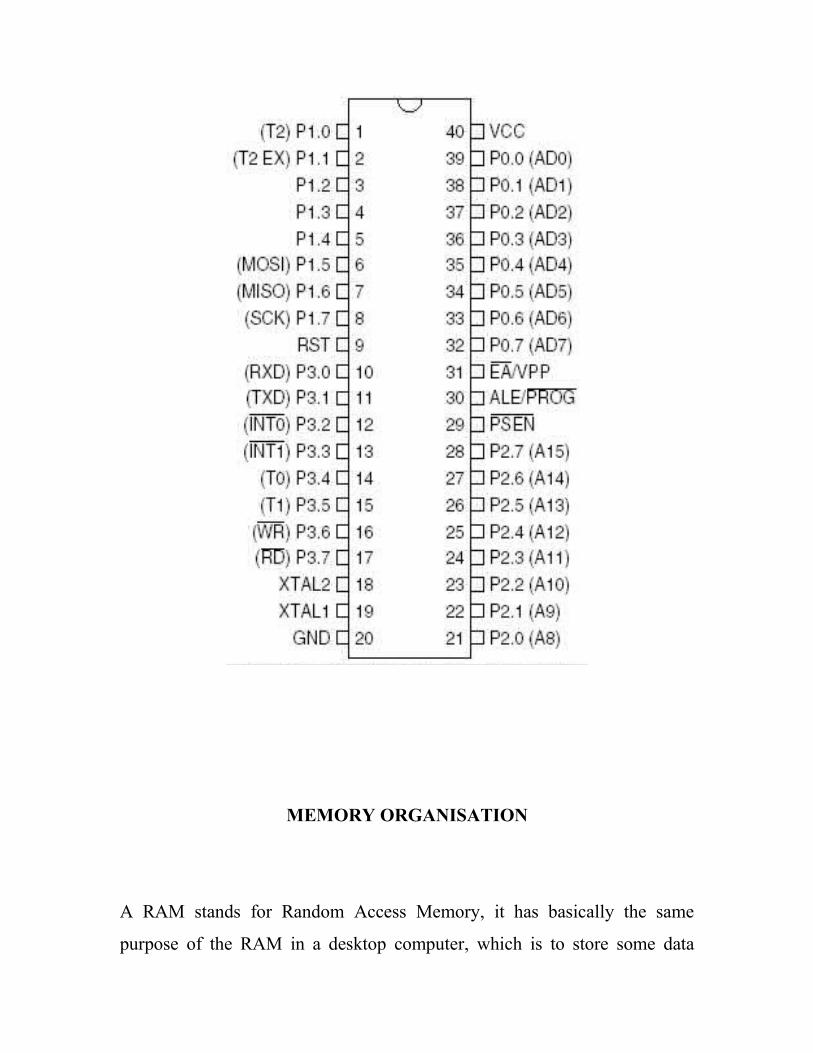
discussed above. Figure 1.2.B shows the pin configuration of the 89S52,
where the function of each pin is written next to it, and, if it exists, the dual
function is written between brackets. The pins are written in the same order

as in the block diagram of figure 1.2.A, except for the VCC and GND pins
which I usually note at the top and the bottom of any device.
Note that the pin that have dual functions, can still be used normally as an
input/output pin. Unless you program uses their dual functions, All the 32
I/O pins of the microcontroller are configured as input/output pins.

Most of the function of the pins of the 89S52 microcontroller will be
discussed in detail, except for the pins required to control an external
memory, which are the pins number 29, 30 and 31.
Since we are not going to use any external memory, pins 29 and 30 will be
ignored through all the report, and pin 31 (EA) always connected to VCC (5
Volts) to enable the micro-controller to use the internal on chip memory
rather than an external one (connecting the pin 31 to ground would indicate
to the microcontroller that an external memory is to be used instead of the
internal one).
MEMORY ORGANISATION
A RAM stands for Random Access Memory, it has basically the same
purpose of the RAM in a desktop computer, which is to store some data

required during the execution time of different programs. While an
EEPROM, also called FLASH memory is a more elaborated ROM (Read
Only Memory) which is the memory where the program being executed is
stored. Even if that's not exactly true, you can compare an EEPROM to the
Hard-Disk of a desktop computer from a general point of view. The
EEPROM term stands for Electronically Erasable and Programmable Read
Only Memory.
In microcontrollers, like in any digital system, memory is organized in
Registers, Which is the basic unit of construction of a memory. Each register
is composed of a number of bits (usually 8) where the data can be stored. In
the 8051 family of microcontrollers for example, most registers
are 8-bit register, capable of storing values
ranging from 0 to 255. In order to use bigger
values, various register can be used
simultaneously. Figure 1.3.A shows a typical 8-
bit registers, where the notation D0 to D7
stands for the 8 DATA bits of the register.
Typical register
D7 D6 D5 D4 D3 D2 D1 D0
Figure 1.3.A
As you shall see, the RAM memory of the 89S52, which contains 256
registers, is divided into two main parts, the GPR part, and the SFR part.
GPR stands for 'General Purpose Register' and are the registers that you can
use to store any data during the execution of your program. SFRs (Special
function Register) are registers used to control the functioning of the
microcontroller and to assist the processor through the various operations
being executed. For example, SFRs can be used to control Input/output lines,
to retrieve data transmitted through the serial port of a desktop computer, or
to configure one of the on-chip counters and timers.
In a memory each register has a specific address which is used by the
processor to read and write from specific memory location. Figure 1.3.B
shows the memory organization of the 256 registers of the RAM of the
89S52 microcontroller. The address is noted in Hexadecimal format as this
notation simplifies digital logic calculations for the designers, 00
corresponds to the first location and FF which is equal to 256 corresponds to
the last location.
CLOCK CONCEPT
The clock concept is found in all modern digital electronics, it is a simple
circuit that will generate pulses of electricity at a very specific frequency.
Those pulses will cadence all the events happening inside a microcontroller,
those pulses will also assure the synchronization of the events between
various components inside the microcontroller. For example, if the CPU is
waiting for some result of mathematical operation from the ALU
(Arithmetic and Logic Unit), it will be known - according to very specific
protocol - when and where the resulting data will be delivered to the CPU.
The synchronization of those two devices is maintained because they share
the same clock.

The clock has another very important role which is to enable the
microcontroller to count timing, without a precise clock, it would be
impossible to build a 'Real Time System', or any other device that relies on
time measurements. It can be deduced that the precision of the timing of a
microcontroller depends on the frequency of its clock.
In the 89S52 microcontroller, the clock can be fixed to different value by
connecting a crystal to the pins 18 and 19. Those crystals are sold with the
frequency written on them in Mega Hertz. The maximum operating
frequency of the AT89S52 is 33Mhz, however other manufacturers like
PHILIPS built similar 8051 microcontrollers that can run at frequencies up
to 120 Mhz.
Life cycle of a microcontroller project
Before passing to the next part of the report, it is important to have a general
idea of the steps that are followed to realize a project, from the very
beginning when you get an idea to the very end when you finalize your
project.
As you can see in figure 1.5.A, after you settle on the choice of your project
in the 'brain storming' part, its imperative to imagine how it can be
implemented from the hardware point of view, before passing to the
programming phase, because programming is much more flexible than the
hardware design. In other words, you start by designing the hardware, then

you work on the programming while taking in consideration the eventual
constraints imposed by the hardware design.
Fig 1.5.A
The hardware design includes all the aspects of the electronic connections
between other devices, like the compatibility of the voltage levels, or the
required number of pins, etc...
After you're done with a first version of your program, you can transfer it to
the microcontroller mounted on the board that you realized already, resulting
in a first prototype. The transfer of the code is done using a special device
called 'burner' or 'programmer' that connect to the computer, reads the HEX
file generated by the compiler, and sends it to the 'program memory' of the
microcontroller. The prototype will be used to test your project, correct
eventual errors and enhance its performance, tacking in account the famous

rule that states that any project never works the first time, at least it does not
work as you expected!
Your project will always stay in the prototyping cycle, even if you decide
that it is functioning correctly, simply because perfect machines or
inventions do not exist, so there is always some room for little changes and
updates.

I/O port detailed structure
It is important to have some basic notions about the structure of an I/O port
in the 8051 architecture. You will notice along this report how this will
affect our choices when it comes to connect I/O devices to the ports.
Actually, the I/O ports configuration and mechanism of the 8051 can be
confusing, due to the fact that a pin acts as an output pin as well as an input
pin in the same time.
Figure 3.1.A shows the internal diagram of a single I/O pin of port 1. The
first thing you have to notice is that there are tow different direction for the
data flow from the microcontroller's processor and the external pin: The
Latch value and the Pin value. The latch value is the value that the
microcontroller tries to output on the pin, whiles the pin value, is the actual
logic state of the pin, regardless of the latch value that was set by the
processor in the first place. The microcontroller reads the state of a pin
through the Pin value line, and writes through the latch value line. If you
imagine the behavior of the simple circuit in figure 3.1.A, you'll notice that
the I/O pin should follow the voltage of the Latch value, providing 5V
through the pull-up resistor, or 0V by connecting the pin directly to the GND
through the transistor.
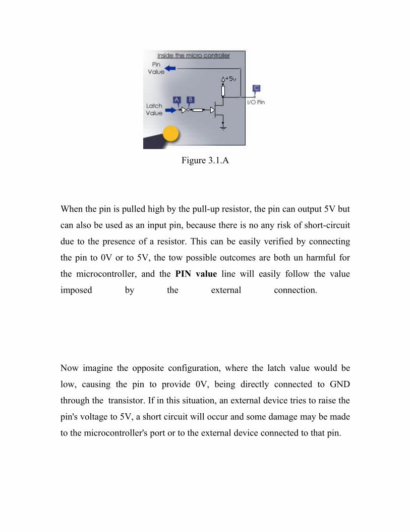
Figure 3.1.A
When the pin is pulled high by the pull-up resistor, the pin can output 5V but
can also be used as an input pin, because there is no any risk of short-circuit
due to the presence of a resistor. This can be easily verified by connecting
the pin to 0V or to 5V, the tow possible outcomes are both un harmful for
the microcontroller, and the PIN value line will easily follow the value
imposed by the external connection.
Now imagine the opposite configuration, where the latch value would be
low, causing the pin to provide 0V, being directly connected to GND
through the transistor. If in this situation, an external device tries to raise the
pin's voltage to 5V, a short circuit will occur and some damage may be made
to the microcontroller's port or to the external device connected to that pin.

To summarize, in the 8051 architecture, to use a PIN as an input pin,
you have to output '1', and the pin value will follow the value imposed
by the device connected to it (switch, sensor, etc...). If you plan to use the
pin as an output pin, then just output the required value without taking
any of this in consideration.
Even if some ports like P3 and P0 can have a slightly different internal
composition than P1, due to the dual functions they assure, understanding
the structure and functioning of port 1 as described above is fairly enough to
use all the ports for basic I/O operations.

Introduction to 89S52 Peripherals
Figure 4.1 below shows a simplified diagram of the main peripherals present
in the 89S52 and their interaction with the CPU and with the external I/O
pins. You can notice that there are 3 timers/Counters. We use the expression
"Timer/Counter" because this unit can be a counter when it counts external
pulses on it's corresponding pin, and it can be a timer when it counts the
pulses provided by the main clock oscillator of the microcontroller.
Timer/Counter 2 is a special counter, that does not behave like the tow
others, because it have a couple of extra functionality.
The serial port, using a UART (Universal Asynchronous Receive Transmit)
protocol can be used in a wide range of communication applications. With
the UART provided in the 89S52 you can easily communicate with a serial
port equipped computer, as well as communicate with another
microcontroller. This last application, called Multi-processor
communication, is quite interesting, and can be easily implemented with 2
89S52 microcontrollers to build a very powerful multi-processor controllers.
If all the peripherals described above can generate interrupt signals in the
CPU according to some specific events, it can be useful to generate an
interrupt signal from an external device, that may be a sensor or a Digital to
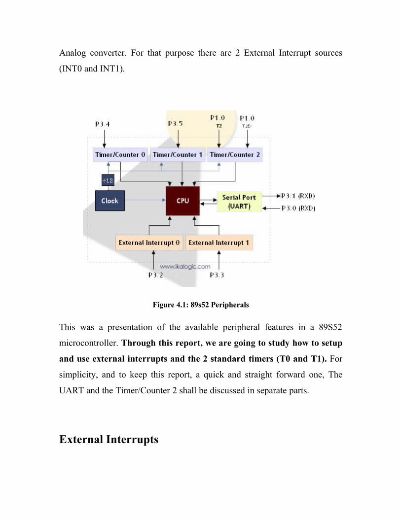
Analog converter. For that purpose there are 2 External Interrupt sources
(INT0 and INT1).
Figure 4.1: 89s52 Peripherals
This was a presentation of the available peripheral features in a 89S52
microcontroller. Through this report, we are going to study how to setup
and use external interrupts and the 2 standard timers (T0 and T1). For
simplicity, and to keep this report, a quick and straight forward one, The
UART and the Timer/Counter 2 shall be discussed in separate parts.
External Interrupts

Let's start with the simplest peripheral which is the external interrupt, which
can be used to cause interruptions on external events (a pin changing its state
from 0 to 1 or vice-versa). Interruption is a mean of stopping the flow of a
program, as a response to a certain event, to execute a small program called
'interrupt routine'.
As we noticed in figure 4.1, in the 89S52, there are two external interrupt
sources, one connected to the pin P3.2 and the other to P3.3. They are
configured using a number of SFRs (Special Function Registers). Most of
those SFRs are shared by other peripherals as you shall see in the rest of the
part.
The IE register
Figure 4.2.A: IE Register
The first register we have to configure (by turning On or Off the right
bits) is the IE register, shown in figure 4.2.A. IE stands for 'Interrupt
Enable', and it is used to allow different peripherals to cause software
interruption. To use any of the interrupts, the bit EA (Enable ALL) must be
set to 1, then, you have enable each one of the interrupts to be used with its
individual enable bit. For the external interrupts, the two bits EX0 and EX1
are used for External Interrupt 0 and External Interrupt 1. The rest of the bits
of IE register are used for other interrupt sources like the 3 timers overflow
(ETx) and the serial interface (ES).

The TCON register
figure 4.2.B: TCON Register
Similarly, you have to set the bits IT0 and IT1 in the TCON register, shown
in figure 4.2.B. The bits IT0/IT1 are used to configure the type of signal on
the corresponding pins (P3.2/P3.3) that generated an interrupt according to
the following table:
IT0/IT1 = 1 External interrupt caused by a falling edge signal on P3.2/P3.3IT0/IT1 = 0 External interrupt caused by a low level signal on P3.2/P3.3
If IT0 or IT1 is set to 0, an interruption will keep reoccurring as long as P3.2
or P3.3 is set to 0. This mode isn't easy to mange, and most programmers
tends to use external interrupts triggered by a falling edge (transition from 1
to 0).

Timer/Counter
The timer is a very interesting peripheral, that is imperatively present in
every microcontroller. It can be used in tow distinct modes:
Timer: Counting internal clock pulses, which are fixed with time, hence, we
can say that it is very precise timer, whose resolution depends on the
frequency of the main CPU clock (note that CPU clock equals the crystal
frequency over 12).
Counter: Counting external pulses (on the corresponding I/O pin), which
can be provided by a rotational encoder, an IR-barrier sensor, or any device
that provide pulses, whose number would be of some interest.
Sure, the CPU of a microcontroller could provide the required timing or
counting, but the timer/counter peripheral relieves the CPU from that
redundant and repetitive task, allowing it to allocate maximum processing
power for more complex calculations.
So, like any other peripheral, a Timer/Counter can ask for an interruption of
the program, which - if enabled - occurs when the counting registers of the
Timer/Counter are full and overflow. More precisely, the interruption will
occur at the same time the counting register will be reinitialized to its initial
value.

INTRODUCTION TO THE PROJECT
Project Definit ion:
Project title is “AUTOMATIC ROOM LIGHT CONTROLLER WITH BIDIRECTIONAL VISITOR
COUNTER “.
The objective of this project is to make a controller based model to count number of persons
visiting particular room and accordingly light up the room. Here we can use sensor and can know
present number of persons.
In today’s world, there is a continuous need for automatic appliances with the increase in
standard of living, there is a sense of urgency for developing circuits that would ease the
complexity of life.
Also if at all one wants to know the number of people present in room so as not to have
congestion. This circuit proves to be helpful.
Project Overview
This Project “Automatic Room Light Controller with Visitor Counter using Microcontroller is a
reliable circuit that takes over the task of controlling the room lights as well us counting number
of persons/ visitors in the room very accurately. When somebody enters into the room then the
counter is incremented by one and the light in the room will be switched ON and when any one
leaves the room then the counter is decremented by one. The light will be only switched OFF
until all the persons in the room go out. The total number of persons inside the room is also
displayed on the seven segment displays.

The microcontroller does the above job. It receives the signals from the sensors, and this signal
is operated under the control of software which is stored in ROM. Microcontroller AT89S52
continuously monitor the Infrared Receivers, When any object pass through the IR Receiver’s
then the IR Rays falling on the receiver are obstructed , this obstruction is sensed by the
Microcontroller
APPLICATION, ADVANTAGES & DISADVANTAGES
• Application
For counting purposes
For automatic room light control
• Advantages
• Disadvantages
.


MICROCONTROLLER MODULE SNAPSHOT
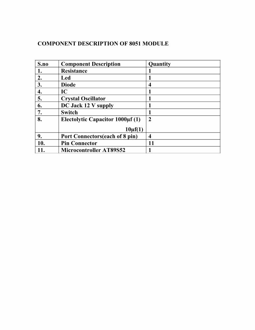
COMPONENT DESCRIPTION OF 8051 MODULE
S.no Component Description Quantity1. Resistance 12. Led 13. Diode 44. IC 15. Crystal Oscillator 16. DC Jack 12 V supply 17. Switch 18. Electolytic Capacitor 1000µf (1)
10µf(1)
2
9. Port Connectors(each of 8 pin) 410. Pin Connector 1111. Microcontroller AT89S52 1

References 1) www.instructables.com/answers/What-is-a-piezoelectric-crystal
2) inhabitat.com/index.php?s=piezoelectric crystal
3) www.aurelienr.com/electronique/ piezo / piezo . pdf
4) www.piezomaterials.com/
5) hyperphysics.phy-astr.gsu.edu/hbase/solids/piezo.html
6) www.iitk.ac.in/directions/dirnet7/P~S-Kamle~F.pdf

7) www. definition -of.net/ piezoelectric
8) piezo.com/tech1terms.html
9) www.treehugger.com
10) ieeexplore.ieee.org/iel5/27/19498/00901194.pdf?arnumber.
11) books.google.co.in/books?isbn=1402046693...