Embed Size (px)
Citation preview

7/29/2019 Synplicity Efficient Dsp
http://slidepdf.com/reader/full/synplicity-efficient-dsp 1/8
Introduction
The use of Digital Signal Processing (DSP) in electronic products is increasing at a phenomenal rate. Field-
Programmable Gate Arrays (FPGAs), with their multi-million equivalent gate counts and DSP-centric features can
offer dramatic performance increases over standard DSP chips. They also offer an attractive alternative for small
and medium volume production FPGAs also make very powerful prototyping and verification vehicles for real-
time emulation of DSP algorithms [1].
This paper discusses the challenges and requirements of creating portable algorithmic IP for FPGAs and ASICs
and illustrates how an ESL synthesis methodology using Synplicity's Synplify ® DSP tool can significantly reduce the
time and effort to implement either technology. The Synplify DSP tool automatically creates optimized logic
implementations for both FPGAs and ASICs.
Challenges In Porting RTL Between FPGA and ASICs
The design team might ask: why is porting RTL between FPGAs and ASICs a problem? After all, isn't RTL
(synthesizable Verilog and VHDL) supposed to make the design portable? The answer can be quite lengthy and
varies depending on the type of design. But for DSP algorithms, a general answer is that the RTL often specifies
the exact mapping of key operations like multipliers, adders, and storage. Another way of saying this is that
although the RTL is portable at the logic level, it is not at the architectural level. If synthesized to a different
target, the same RTL will yield less than ideal results; in a different target technology, the result may be function-
ally correct but very sub-optimal.
Choosing an algorithm architecture involves the basic question of how much pipelining, parallelization, or seriali-
zation is needed to meet the sample rate and throughput requirements of the algorithm. In addition, funda-
mental DSP functions like FIR, FFT, sine, cosine, divide, etc. may have different optimal implementations
depending on the target technologies. A good example is the direct form versus the transposed form of a FIR
filter - one may be better for a particular FPGA device [2], and the other may be better for an ASIC technology.
Different architectures are usually required to get good results from an FPGA versus an ASIC. It's commonly
known that FPGA devices tend to be more register-centric, and many ASIC-to-FPGA porting guidelines recom-
mend lots of pipelining, registering of all ports, and breaking combinatorial logic into smaller portions. This
results in an area increase if done in the ASIC, but might be required to meet timing in the FPGA [2].
For an ASIC target, the opposite is often desired. Register minimization is recommended to reduce area and
power. Higher clock speeds can be exploited using time-multiplexing and resource sharing techniques to mini-
mize multipliers and other expensive operations. Recent designs for the consumer and wireless markets balance
these demands carefully.
One of the inevitable differences between ASIC RTL and FPGA RTL is the use of memory. In an FPGA, standard
memory types are built into the device. Depending on the FPGA tool flow and vendor, specific coding styles are
required to describe storage arrays and memories. High quality FPGA synthesis tools automatically infer memory
use from the RTL. However, in the ASIC world, there are many different memory options available from IP and
fab library vendors. Users select and compile memory for a particular configuration, and instantiate it into the
RTL design.
Synplicity, Inc.White Paper July 2007
Efficient DSP Algorithm Development
for FPGA and ASIC Technologies
Shiv Balakrishnan,Technical Marketing Engineer, and Chris Eddington, Senior Technical Marketing Manager, Synplicity, Inc.

7/29/2019 Synplicity Efficient Dsp
http://slidepdf.com/reader/full/synplicity-efficient-dsp 2/8
There are many articles and resources describing the coding styles and porting techniques needed to move IP
between FPGAs and ASICs. [1, 3, 4] Such techniques include pipelining and building memory wrappers for
handling resets, enables, and other differences between FPGA and ASIC memory interfaces. Suffice to say that it
requires a significant amount of coding, verification, and expertise to move implementations between technology
types.
Additional porting challenges arise in ASIC designs first prototyped in FPGAs. This occurs when real-time stimuliand at-speed verification are required. To support these requirements, it is necessary to maintain bit and sample
accuracy between simulation models, in particular the FPGA implementation and the ASIC model. This can
require a lot of effort especially if the implementations are different or changing rapidly, and the test harness
must be manually modified, compared, and debugged.
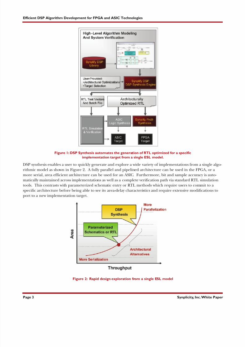
An ESL Synthesis Solution
Synplicity's Synplify DSP tool provides a powerful DSP synthesis methodology which overcomes many of the prob-
lems and issues described above. Synplicity's DSP synthesis concept is based on four key elements:
• Use of Electronic System Level (ESL) models with high levels of architectural and hardware abstraction
• Automatic optimizations based on user-specified sample rates
• User-selected target technologies
• Native support for multi-rate designs
With these elements, the DSP synthesis engine can synthesize different RTL implementations based on user
constraints using system-wide, target-aware optimizations. The RTL, produced with optimized architecture and
coding styles, can then be taken through the standard logic synthesis flow. Figure 1 shows this approach to high-
level design.
By using this ESL synthesis approach, designs are created and maintained at a high-level of abstraction, which
increases portability, shortens development time, and improves the return on engineering effort. Instead of main-
taining the IP at the RTL level, it can be done at the algorithm model level which increases portability and the
return on the algorithm developer's efforts.
Synplicity, Inc.White Paper Page 2
Efficient DSP Algorithm Development for FPGA and ASIC Technologies
7/29/2019 Synplicity Efficient Dsp
http://slidepdf.com/reader/full/synplicity-efficient-dsp 3/8
Figure 1: DSP Synthesis automates the generation of RTL optimized for a specific
implementation target from a single ESL model.
DSP synthesis enables a user to quickly generate and explore a wide variety of implementations from a single algo-
rithmic model as shown in Figure 2. A fully parallel and pipelined architecture can be used in the FPGA, or a
more serial, area efficient architecture can be used for an ASIC. Furthermore, bit and sample accuracy is auto-
matically maintained across implementations as well as a complete verification path via standard RTL simulation
tools. This contrasts with parameterized schematic entry or RTL methods which require users to commit to a
specific architecture before being able to see its area-delay characteristics and require extensive modifications to
port to a new implementation target.
Figure 2: Rapid design exploration from a single ESL model
Synplicity, Inc.White Paper Page 3
Efficient DSP Algorithm Development for FPGA and ASIC Technologies

7/29/2019 Synplicity Efficient Dsp
http://slidepdf.com/reader/full/synplicity-efficient-dsp 4/8
Features For ASIC Targets
As discussed earlier, ASIC technologies and design flows are substantially different from those of FPGAs. As illus-
trated in Figure 1, there are some special features and capabilities required to support ASIC flows. Some of these
features include:
• ASIC lithography performance characterization necessary for architectural optimizations
• Automatic memory extraction for flexible support of memory IP
• Choice of Synchronous/Asynchronous Resets
• RTL optimizations and suitable output files for smooth operation with ASIC logic synthesis flows
These ASIC-specific features, combined with complementary FPGA-specific features allow automatic porting of
ASIC designs to FPGAs or vice versa replacing time-consuming manual coding and translation efforts.
Design Example
We illustrate these benefits with a simple FIR design example which highlights the power of high level modeling
abstraction, architectural DSP synthesis, and target-aware optimizations.
The first step is to create a model that includes fixed-point and sample rate behavior. The Synplify DSP library leverages the powerful quantization and multi-rate features in the Simulink® environment to simplify fixed-point
design capture and verification. The following figure shows a Synplify DSP model of a basic 16-tap FIR filter with
fixed coefficients.
Figure 3: Simulink [5] block diagram of a 16-tap FIR. Also shown are the filter design tool,
input waveform, and output analysis in time and frequency domains.
If we were to examine the specification of the filter itself, some of the key parameters are shown below in Figure 4.
Note that the block inherits the fixed-point data type at the input and automatically propagates the data type
according to user selected settings and the functionality of the internal calculations. During simulation, the exact
quantized, discrete-time behavior can be verified. In addition, powerful analysis tools such as floating-point over-
ride and overflow logging can be used to explore the impact of word length and precision on the algorithm
performance.
Synplicity, Inc.White Paper Page 4
Efficient DSP Algorithm Development for FPGA and ASIC Technologies

7/29/2019 Synplicity Efficient Dsp
http://slidepdf.com/reader/full/synplicity-efficient-dsp 5/8
Figure 4: Parameters of the Synplify DSP FIR filter block. Note specified data formats.
Algorithm Implementation Using DSP Synthesis
Given this algorithmic model we can show the benefits of automatic DSP synthesis and architectural optimizations.
An important detail to note is that the Synplify DSP algorithm model is vendor, technology, and architecture inde-
pendent, that is, the simulation behavior is independent of these implementation choices. Not until the DSP
synthesis step does the user define the target device and select architectural optimization choices. The Synplify
DSP tool then synthesizes an optimized RTL implementation from the model. Figure 5 shows an example selec-tion for an ASIC target.
Of particular note are the Retiming and Folding options. The Retiming option allows the Synplify DSP tool to
modify the architecture to use pipelining and other techniques to get to the desired performance goal, at the
expense of latency at the output. The Folding option allows the design to share hardware, at the expense of lower
throughput (i.e. trade off maximum sample rate for resource utilization).
Synplicity, Inc.White Paper Page 5
Efficient DSP Algorithm Development for FPGA and ASIC Technologies

7/29/2019 Synplicity Efficient Dsp
http://slidepdf.com/reader/full/synplicity-efficient-dsp 6/8
Figure 5: Defining parameters for architectural optimization to an ASIC target.
Architectural Exploration
The power of an automatic DSP synthesis engine is the ability to quickly explore a variety of architectures and
target technologies. This design-space exploration process can lead to a significantly more optimal solution,
especially if one is able to consider a variety of FPGA and ASIC technologies.
In this example, we'll explore the retiming and folding optimizations and show how they offer significant
tradeoffs in speed and area. First, we generate 4 cases of the 10 MHz 64-tap FIR filter in a Virtex-4 FPGA: a base-
line and three different folding factors for area reduction. The results are generated by logic synthesis of the
Synplify DSP RTL.
Table 1: Impact of automatically synthesized folding optimizations on filter
throughput and HW sharing for Virtex-4 FPGA
A similar analysis for an ASIC implementation of the same design is shown below in Table 2, which shows the area
difference in a 90nm technology for the two extremes i.e. fully parallel vs. fully serial implementation.
Synplicity, Inc.White Paper Page 6
Efficient DSP Algorithm Development for FPGA and ASIC Technologies
414.5 MHz > 400 Ms/s 16
4 346.7 MHz 86.7 Ms/s 4
8 352.0 MHz 44 Ms/s 2
16 338.5 MHz 21.2 Ms/s 1
Folding Factor Est. Frequency Max. Throughput DSP48 Slices
None

7/29/2019 Synplicity Efficient Dsp
http://slidepdf.com/reader/full/synplicity-efficient-dsp 7/8
* indicates the unit of area is scaled by 2.8 sq nm which is the approximate of a two-input NAND gate
** Multipliers are implemented with logic (gates)
*** Extracted memory is dual ported
Table 2: Serialization and hardware sharing allows implementing the 65-tap FIR filter in half the area
What we observe from Table 2 is that DSP synthesis provides area improvements automatically when lower sample
rates permit shared hardware. Alternatively, the powerful ESL capability permits easy mapping to different tech-
nologies while exploiting higher clock frequencies. At the same time, working from a single algorithmic model
eliminates the need to change or re-verify the model.
Conclusion
The simple FIR example above shows that the Synplify DSP software provides a rapid and efficient means of
making architectural tradeoffs based on accurate simulation of their relative performance and area. This enables
the user to explore multiple architectural possibilities, including important implementation details such as fixed
point considerations, while efficiently obtaining useful cost versus performance data. The result is optimal FPGA
and ASIC implementation of high level algorithms while minimizing design time.
The EDA industry seems to be evolving towards delivering on early promises of ESL design [6], both in an
integrated design flow for hardware prototypes as well as shipping systems [7]. Improvements to tools such as
Synplify DSP will be crucial to further this advance in performance-sensitive applications.
References:
1.“System Integration and Testing Before First Hardware Availability? It's Possible!” M. Serughetti,
CoWare, Inc., SoC Central, March 1, 2007.
2. 'DSP: Designing for Optimal Results”, Advanced Design Guide, Xilinx Inc., 2005
3.“Efficient Development of Wireless IP with High Level Modeling and Synthesis“, C. Eddington, Oct., 2006.
4.”Software-Intensive ASICS/ASSPs Demand Integrated Prototyping Solutions”, A. Haines, Synplicity Inc.,
EDA DesignLine, June, 2007.
5.MATLAB R2006b, Version 7.3.0.267, the MathWorks, Aug. 2006
6.“Focusing on Primary ESL Design Solutions”, S.Bloch,http://www.chipdesignmag.com/display.php?articleId=879
7.“Design Community Trend Survey Reveals Hidden Market for ESL and FPGA”,
http://www.embeddedstar.com/press/content/2005/9/embedded18796.html
Synplicity, Inc.White Paper Page 7
Efficient DSP Algorithm Development for FPGA and ASIC Technologies
90nm Baseline(parallel)
10 53000 64 ** 0 53000
90nmFolding = 64(serial)
640 MHz 11000 1 9800 *** 20800
Architecture
Extracted clock
(MHZ)
Logic Area
(gates)
*2.8 sq nm
# of 18x18 bit
Multiplies
Memory
(equiv. gates)*
2.8 * (sq nm)Total core
area (sq nm)

7/29/2019 Synplicity Efficient Dsp
http://slidepdf.com/reader/full/synplicity-efficient-dsp 8/8
Synplicity, Inc.600 W. California Ave, Sunnyvale, CA 94086Phone: (408) 215-6000, Fax: (408) 222-0264 www.synplicity.com
Copyright © 2007 Synplicity, Inc. All rights reserved. Specifications subject to change withoutnotice. Synplicity,the Synplicity logo,“Simply Better Results”, and Synplify are registered trademarksof Synplicity,Inc. All other names mentioned herein are trademarks or registered trademarks of their respective companies.
Synplicity, Inc.White Paper Page 8
Efficient DSP Algorithm Development for FPGA and ASIC Technologies