Embed Size (px)
Citation preview
06) 2073–2075www.elsevier.com/locate/matlet
Materials Letters 60 (20
Synthesis of carbon nanocoils on surface morphologychanged silicon substrates
Z.Y. Huang, X. Chen, J.R. Huang, M.Q. Li, J.H. Liu ⁎
Center for Biomimetic Sensing and Control Research, Institute of Intelligent Machines, Chinese Academy of Sciences, Hefei, Anhui 230031, PR China
Received 16 May 2005; accepted 22 December 2005Available online 17 January 2006
Abstract
By the controlled corrosion of HF, silicon substrates appeared to be in a state of concavo-convex morphology. Carbon nanocoils weresynthesized on these silicon substrates by the pyrolysis of acetylene with catalytic thermal chemical vapor deposition (CVD). Scanning electronmicroscopy and transmission electron microscopy were carried out to observe the regular morphology of carbon nanocoils, while Raman spectrawas used to characterize the graphitization degree. The growing process of the nanocoils was regarded as the anisotropic activity of catalystparticles resulting from the different thicknesses of FeO layer.© 2005 Elsevier B.V. All rights reserved.
Keywords: Carbon nanocoils; Chemical vapor deposition; Silicon substrate
1. Introduction
Since the discovery of carbon nanotubes (CNTs) by Iijima[1], great interest has been focused on the physical and electricproperties of these novel materials. Besides straight carbonnanotubes, carbon nanocoils (coiled carbon nanofibers andcoiled carbon nanotubes) were also predicated and observedexperimentally [2]. Because of the intrinsical structure, theirproperties [3–5] and potential applications as mechanicalcomponents such as resonating elements [6,7] and nanospringsare widely researched. Several methods are used for thesynthesis of carbon nanocoils. As for carbon nanocoils, catalyticchemical vapor deposition (CCVD) is more effective than othermethods. Generally, nanotubes prepared by the CCVD methodare in straight or randomly curled morphologies. So far eitherspecific process conditions [8] or a special catalyst [9–12] isavailable for the synthesis of carbon nanocoils. Little researchhas been focused on changing the surface morphology ofsubstrate. Bai [13] produced pure coiled carbon structures onthe porous aluminum surface of oxide films. In the present
⁎ Corresponding author. Tel.: +86 551 5591 142; fax: +86 551 5592 420.E-mail address: [email protected] (J.H. Liu).
0167-577X/$ - see front matter © 2005 Elsevier B.V. All rights reserved.doi:10.1016/j.matlet.2005.12.103
work, silicon substrates were corroded by HF firstly, whichshowed concavo-convex surface morphology. Carbon nano-coils were then synthesized on these silicon substrates by thepyrolysis of acetylene with catalytic thermal chemical vapordeposition. By changing the surface morphology of siliconsubstrates, regular carbon nanocoils can be obtained whilemultiwall carbon nanotubes (MWCNTs) were obtained for thenon-corroded Si substrate. Scanning probe microscope (AutoP-robe CP, Veeco, America) was used for the observation of thesurface of corroded silicon substrate. Field emission scanningelectron microscopy (FE-SEM, FEI Sirion 200 FEG, America)
Fig. 1. FE-SEM micrographs for the surface morphology of (a) non-corrodedand (b) corroded silicon substrate.
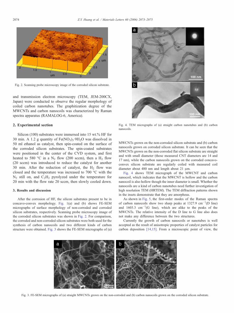
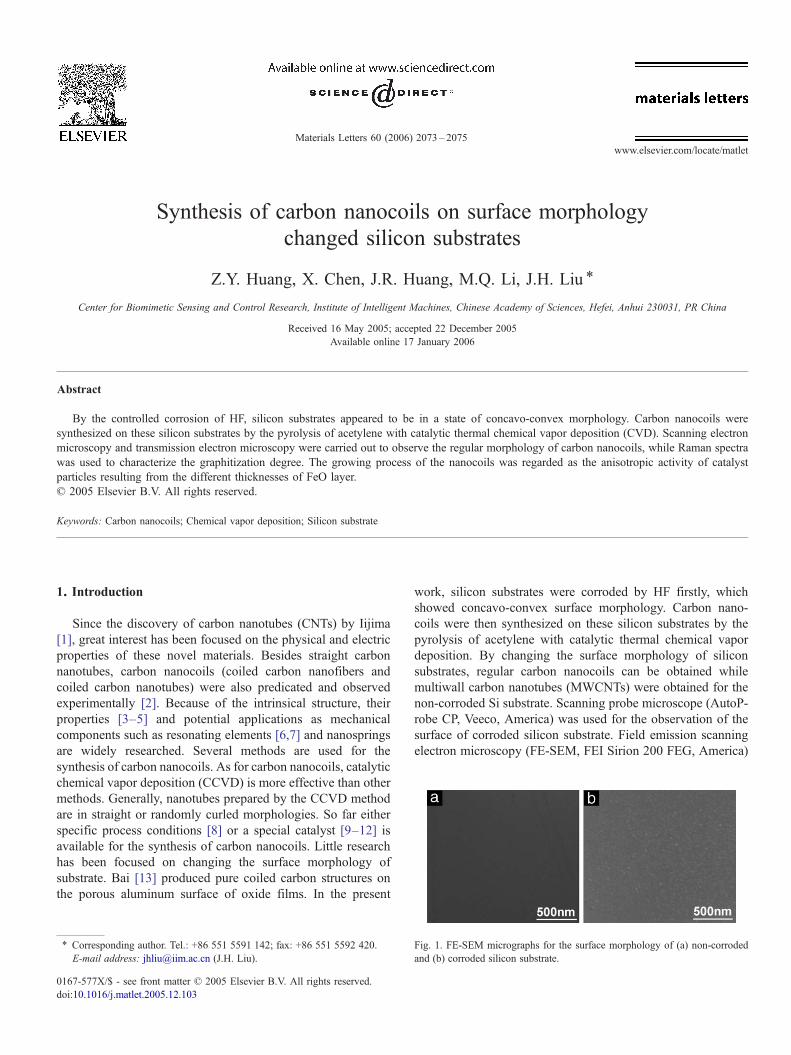
Fig. 2. Scanning probe microscopy image of the corroded silicon substrate.
Fig. 4. TEM micrographs of (a) straight carbon nanotubes and (b) carbonnanocoils.
2074 Z.Y. Huang et al. / Materials Letters 60 (2006) 2073–2075
and transmission electron microscopy (TEM, JEM-200CX,Japan) were conducted to observe the regular morphology ofcoiled carbon nanotubes. The graphitization degree of theMWCNTs and carbon nanocoils was characterized by Ramanspectra apparatus (RAMALOG-6, America).
2. Experimental section
Silicon (100) substrates were immersed into 15 wt.% HF for30 min. A 1.2 g quantity of Fe(NO3)3·9H2O was dissolved in50 ml ethanol as catalyst, then spin-coated on the surface ofthe corroded silicon substrates. The spin-coated substrateswere positioned in the center of the CVD system, and firstheated to 580 °C in a N2 flow (200 sccm), then a H2 flow(20 sccm) was introduced to reduce the catalyst for another30 min. After the reduction of catalyst, the H2 flow wasclosed and the temperature was increased to 700 °C with theN2 still on, and C2H2 pyrolyzed under the temperature for20 min with the flow rate 20 sccm, then slowly cooled down.
3. Results and discussion
After the corrosion of HF, the silicon substrates present to be inconcavo-convex morphology. Fig. 1(a) and (b) shows FE-SEMmicrographs of surface morphology of non-corroded and corrodedsilicon substrates, respectively. Scanning probe microscopy image ofthe corroded silicon substrates was shown in Fig. 2. For comparison,the corroded and non-corroded silicon substrates were both used for thesynthesis of carbon nanocoils and two different kinds of carbonstructure were obtained. Fig. 3 shows the FE-SEM micrographs of (a)
Fig. 3. FE-SEM micrographs of (a) straight MWCNTs grown on the non-cor
MWCNTs grown on the non-corroded silicon substrate and (b) carbonnanocoils grown on corroded silicon substrate. It can be seen that theMWCNTs grown on the non-corroded flat silicon substrate are straightand with small diameter (those measured CNT diameters are 14 and17 nm), while the carbon nanocoils grown on the corroded concavo-convex silicon substrate are regularly coiled with measured coildiameter about 480 nm and length about 21 μm.
Fig. 4 shows TEM micrograph of the MWCNT and carbonnanocoil, which indicates that the MWCNT is hollow and the carbonnanocoil is also hollow though the inner diameter is small. Whether thenanocoils are a kind of carbon nanotubes need further investigation ofhigh resolution TEM (HRTEM). The TEM diffraction patterns shownin the insets demonstrate that they are amorphous.
As shown in Fig. 5, the first-order modes of the Raman spectraof carbon nanocoils show two sharp peaks at 1327.9 cm–1(D line)and 1603.3 cm–1(G line), which are alike to the peaks of theMWCNTs. The relative intensity of the D line to G line also doesnot make any difference between the two structures.
Currently the growth of carbon nanocoils or nanotubes is wellaccepted as the result of anisotropic properties of catalyst particles forcarbon deposition [14,15]. From a microscopic point of view, the
roded and (b) carbon nanocoils grown on the corroded silicon substrate.
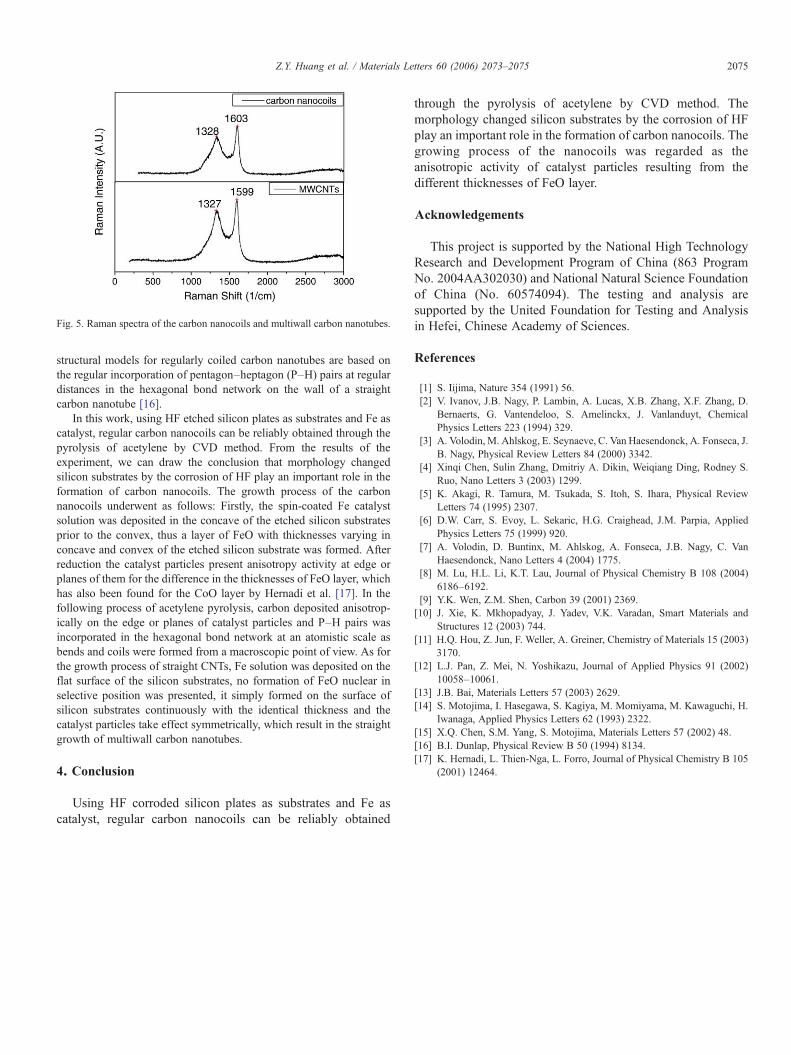
Fig. 5. Raman spectra of the carbon nanocoils and multiwall carbon nanotubes.
2075Z.Y. Huang et al. / Materials Letters 60 (2006) 2073–2075
structural models for regularly coiled carbon nanotubes are based onthe regular incorporation of pentagon–heptagon (P–H) pairs at regulardistances in the hexagonal bond network on the wall of a straightcarbon nanotube [16].
In this work, using HF etched silicon plates as substrates and Fe ascatalyst, regular carbon nanocoils can be reliably obtained through thepyrolysis of acetylene by CVD method. From the results of theexperiment, we can draw the conclusion that morphology changedsilicon substrates by the corrosion of HF play an important role in theformation of carbon nanocoils. The growth process of the carbonnanocoils underwent as follows: Firstly, the spin-coated Fe catalystsolution was deposited in the concave of the etched silicon substratesprior to the convex, thus a layer of FeO with thicknesses varying inconcave and convex of the etched silicon substrate was formed. Afterreduction the catalyst particles present anisotropy activity at edge orplanes of them for the difference in the thicknesses of FeO layer, whichhas also been found for the CoO layer by Hernadi et al. [17]. In thefollowing process of acetylene pyrolysis, carbon deposited anisotrop-ically on the edge or planes of catalyst particles and P–H pairs wasincorporated in the hexagonal bond network at an atomistic scale asbends and coils were formed from a macroscopic point of view. As forthe growth process of straight CNTs, Fe solution was deposited on theflat surface of the silicon substrates, no formation of FeO nuclear inselective position was presented, it simply formed on the surface ofsilicon substrates continuously with the identical thickness and thecatalyst particles take effect symmetrically, which result in the straightgrowth of multiwall carbon nanotubes.
4. Conclusion
Using HF corroded silicon plates as substrates and Fe ascatalyst, regular carbon nanocoils can be reliably obtained
through the pyrolysis of acetylene by CVD method. Themorphology changed silicon substrates by the corrosion of HFplay an important role in the formation of carbon nanocoils. Thegrowing process of the nanocoils was regarded as theanisotropic activity of catalyst particles resulting from thedifferent thicknesses of FeO layer.
Acknowledgements
This project is supported by the National High TechnologyResearch and Development Program of China (863 ProgramNo. 2004AA302030) and National Natural Science Foundationof China (No. 60574094). The testing and analysis aresupported by the United Foundation for Testing and Analysisin Hefei, Chinese Academy of Sciences.
References
[1] S. Iijima, Nature 354 (1991) 56.[2] V. Ivanov, J.B. Nagy, P. Lambin, A. Lucas, X.B. Zhang, X.F. Zhang, D.
Bernaerts, G. Vantendeloo, S. Amelinckx, J. Vanlanduyt, ChemicalPhysics Letters 223 (1994) 329.
[3] A. Volodin, M. Ahlskog, E. Seynaeve, C. Van Haesendonck, A. Fonseca, J.B. Nagy, Physical Review Letters 84 (2000) 3342.
[4] Xinqi Chen, Sulin Zhang, Dmitriy A. Dikin, Weiqiang Ding, Rodney S.Ruo, Nano Letters 3 (2003) 1299.
[5] K. Akagi, R. Tamura, M. Tsukada, S. Itoh, S. Ihara, Physical ReviewLetters 74 (1995) 2307.
[6] D.W. Carr, S. Evoy, L. Sekaric, H.G. Craighead, J.M. Parpia, AppliedPhysics Letters 75 (1999) 920.
[7] A. Volodin, D. Buntinx, M. Ahlskog, A. Fonseca, J.B. Nagy, C. VanHaesendonck, Nano Letters 4 (2004) 1775.
[8] M. Lu, H.L. Li, K.T. Lau, Journal of Physical Chemistry B 108 (2004)6186–6192.
[9] Y.K. Wen, Z.M. Shen, Carbon 39 (2001) 2369.[10] J. Xie, K. Mkhopadyay, J. Yadev, V.K. Varadan, Smart Materials and
Structures 12 (2003) 744.[11] H.Q. Hou, Z. Jun, F. Weller, A. Greiner, Chemistry of Materials 15 (2003)
3170.[12] L.J. Pan, Z. Mei, N. Yoshikazu, Journal of Applied Physics 91 (2002)
10058–10061.[13] J.B. Bai, Materials Letters 57 (2003) 2629.[14] S. Motojima, I. Hasegawa, S. Kagiya, M. Momiyama, M. Kawaguchi, H.
Iwanaga, Applied Physics Letters 62 (1993) 2322.[15] X.Q. Chen, S.M. Yang, S. Motojima, Materials Letters 57 (2002) 48.[16] B.I. Dunlap, Physical Review B 50 (1994) 8134.[17] K. Hernadi, L. Thien-Nga, L. Forro, Journal of Physical Chemistry B 105
(2001) 12464.