Embed Size (px)
Citation preview
Synthesis


Copyright Notice Copyright 1994-2007 Agilent Technologies, Inc. All rights reserved.
Notice The information contained in this document is subject to change without notice.
Agilent Technologies makes no warranty of any kind with regard to this material, including, but not limited to, the implied warranties of merchantability and fitness for a particular purpose. Agilent Technologies shall not be liable for errors contained herein or for incidental or consequential damages in connection with the furnishing, performance, or use of this material.
Warranty A copy of the specific warranty terms that apply to this software product is available upon request from your Agilent Technologies representative.
U.S. Government Restricted Rights Software and technical data rights granted to the federal government include only those rights customarily provided to end user customers. Agilent provides this customary commercial license in Software and technical data pursuant to FAR 12.211 (Technical Data) and 12.212 (Computer Software) and, for the Department of Defense, DFARS 252.227-7015 (Technical Data - Commercial Items) and DFARS 227.7202-3 (Rights in Commercial Computer Software or Computer Software Documentation).
© Agilent Technologies, Inc. 1994-2007
395 Page Mill Road, Palo Alto, CA 94304 U.S.A.
Acknowledgments Mentor Graphics is a trademark of Mentor Graphics Corporation in the U.S. and other countries.
Microsoft®, Windows®, MS Windows®, Windows NT®, and MS-DOS® are U.S. registered trademarks of Microsoft Corporation.
Pentium® is a U.S. registered trademark of Intel Corporation.
PostScript® and Acrobat® are trademarks of Adobe Systems Incorporated.
UNIX® is a registered trademark of the Open Group.
Java(TM) is a U.S. trademark of Sun Microsystems, Inc.
SystemC® is a registered trademark of Open SystemC Initiative, Inc. in the United States and other countries and is used with permission.
Drawing Interchange file (DXF) is a trademark of Auto Desk, Inc.

EMPOWER/ML, GENESYS, SPECTRASYS, HARBEC, and TESTLINK are trademarks of Eagleware-Elanix Corporation.
GDSII is a trademark of Calma Company.
Sonnet is a registered trademark of Sonnet Software, Inc.

v
Table Of Contents
Chapter 1: Introduction...............................................................................................................1 Overview..............................................................................................................................................1
Chapter 2: A/FILTER.................................................................................................................3
A/FILTER: Types .............................................................................................................................3 Overview..........................................................................................................................................3 GIC Transform Fundamentals ....................................................................................................4 Lowpass All-Pole Minimum Inductor ........................................................................................7 All-Pole Minimum Capacitor .......................................................................................................7 Lowpass All-Pole Single Feedback..............................................................................................8 Lowpass All-Pole Multiple Feedback..........................................................................................8 Lowpass All-Pole Low Sensitivity ...............................................................................................9 Lowpass All-Pole VCVS (Voltage Controlled Voltage Source) .............................................9 Lowpass All-Pole State Variable (Biquad)............................................................................... 10 Lowpass Elliptic Minimum Capacitor ..................................................................................... 10 Lowpass Elliptic VCVS.............................................................................................................. 11 Lowpass Elliptic State Variable................................................................................................. 11 Highpass All-Pole Minimum Inductor .................................................................................... 12 Highpass All-Pole Minimum Capacitor................................................................................... 13 Highpass All-Pole Single Feedback.......................................................................................... 14 Highpass All-Pole Multiple Feedback...................................................................................... 14 Highpass All-Pole Low Sensitivity ........................................................................................... 15 Highpass All-Pole VCVS (Voltage Controlled Voltage Source) ......................................... 15 Highpass All-Pole State Variable .............................................................................................. 16 Highpass Elliptic Minimum Inductor...................................................................................... 16 Highpass Elliptic VCVS ............................................................................................................. 17 Highpass Elliptic State Variable................................................................................................ 17 Bandpass All-Pole Top C........................................................................................................... 18 Bandpass All-Pole Top L........................................................................................................... 19 Bandpass All-Pole Multiple Feedback ..................................................................................... 19 Bandpass All-Pole Multiple Feedback Max Gain .................................................................. 20 Bandpass All-Pole Dual Amplifier ........................................................................................... 20 Bandpass All-Pole Dual Amplifier Max Gain ........................................................................ 21 Bandpass All-Pole Low Sensitivity ........................................................................................... 21 Bandpass All-Pole State Variable.............................................................................................. 22 Bandpass Elliptic VCVS............................................................................................................. 22
Synthesis
vi
Bandpass Elliptic State Variable................................................................................................ 23 Bandstop All-Pole VCVS........................................................................................................... 23 Bandstop All-Pole State Variable.............................................................................................. 24
A/FILTER: Operation................................................................................................................... 24 Active Filter Synthesis Overview.............................................................................................. 24 Walkthrough................................................................................................................................. 25 Parameters..................................................................................................................................... 26
Chapter 3: EQUALIZE ............................................................................................................ 29
EQUALIZE: Operation................................................................................................................. 29 Overview....................................................................................................................................... 29 Equalize Walkthrough ................................................................................................................ 29 Section Types ............................................................................................................................... 31 Finite Q Components ................................................................................................................. 34 Equalizing Measured Data ......................................................................................................... 35 Multiple Section Equalizers ....................................................................................................... 35 Group Delay Discontinuities..................................................................................................... 36 Exponent of the Error Function .............................................................................................. 36 Delay Lines ................................................................................................................................... 37
EQUALIZE: Concepts .................................................................................................................. 38 Definitions .................................................................................................................................... 38 Lowpass and Bandpass Group Delay ...................................................................................... 39 Highpass and Bandstop group delay........................................................................................ 40 All-Pass Networks ....................................................................................................................... 40 Delay Symmetry........................................................................................................................... 40 Repairing poor symmetry........................................................................................................... 41
Chapter 4: FILTER................................................................................................................... 43
FILTER: Operation ........................................................................................................................ 43 Overview....................................................................................................................................... 43 Walkthrough................................................................................................................................. 43
FILTER: Types................................................................................................................................ 50 Overview....................................................................................................................................... 50 Monotonic or Elliptic ................................................................................................................. 50 Minimum Inductor All-Pole Lowpass Minimum Capacitor All-Pole Lowpass................ 51 Minimum Inductor All-Pole Highpass Minimum Capacitor All-Pole Highpass.............. 52 Minimum Inductor All-Pole Bandpass.................................................................................... 53 Minimum Capacitor All-Pole Bandpass .................................................................................. 54 Coupled All-Pole Bandpass Filter Types................................................................................. 54 Top C Coupled All-Pole Bandpass........................................................................................... 56 Top L Coupled All-Pole Bandpass........................................................................................... 57

Table Of Contents
vii
Shunt C Coupled All-Pole Bandpass........................................................................................ 58 Tubular All-Pole Bandpass ........................................................................................................ 59 Blinchikoff 4th Order Flat Delay All-Pole Bandpass............................................................ 59 Symmetry Preserving All-Pole Bandpass ................................................................................ 60 Symmetric Transform................................................................................................................. 60 Top C Coupled TEM Resonator Bandpass........................................................................... 64 Full Transform All-Pole Bandstop........................................................................................... 64 Minimum Inductor Elliptic Lowpass Minimum Capacitor Elliptic Lowpass................... 65 Minimum Inductor Elliptic Highpass Minimum Capacitor Elliptic Highpass ................. 66 Full Transform Elliptic Bandpass............................................................................................. 66 Minimum Inductor ("Zig Zag") Elliptic Bandpass................................................................ 67 Elliptic Parametric Bandpass Filter .......................................................................................... 68 Elliptic Bandstop ......................................................................................................................... 69
Chapter 5: MATCH................................................................................................................... 71
MATCH: Operation........................................................................................................................ 71 Overview....................................................................................................................................... 71 Walkthrough................................................................................................................................. 72 Matching to device data.............................................................................................................. 76 Unstable devices .......................................................................................................................... 76 Custom Networks ....................................................................................................................... 76 How MATCH Works................................................................................................................. 76 Defaults Tab................................................................................................................................. 77 Summary Tab ............................................................................................................................... 78
MATCH: Network Types .............................................................................................................. 78 L-C Pi and Tee Networks .......................................................................................................... 78 LC Bandpass................................................................................................................................. 79 LC Pseudo Lowpass.................................................................................................................... 80 TRL 1/4 Wave............................................................................................................................. 80 TRL Single/Double Stub........................................................................................................... 80 TRL Pseudo Lowpass................................................................................................................. 81 TRL Stepped Impedance ........................................................................................................... 81 Custom.......................................................................................................................................... 81
Chapter 6: MIXER ....................................................................................................................83
MIXER: Operation ......................................................................................................................... 83 Operation Overview ................................................................................................................... 83 Simulation Outputs and Settings .............................................................................................. 90
MIXER: Types................................................................................................................................. 91 Mixer Type Overview................................................................................................................. 91 Diode Single Ended Basic.......................................................................................................... 92
Synthesis
viii
2. Bipolar Differential ................................................................................................................. 93 3. JFET Transformer Single Balanced ..................................................................................... 95 4. Diode Branch Line Single Balanced..................................................................................... 96 5. Diode Transformer Single Balanced.................................................................................... 97 6. JFET Single Ended ................................................................................................................. 99 7. Diode Transformer Double Balanced ............................................................................... 101 8. Bipolar Single Ended ............................................................................................................ 102 9. Bipolar Transformer Single Balanced ................................................................................ 104 10. Bipolar Double Balanced Gilbert ..................................................................................... 106 11. Diode Rat Race Single Balanced....................................................................................... 108
Chapter 7: M/FILTER............................................................................................................ 111 M/FILTER: Operation ................................................................................................................ 111
Overview..................................................................................................................................... 111 Walkthrough............................................................................................................................... 111
M/FILTER: Types........................................................................................................................ 118 Overview..................................................................................................................................... 118 Filter Shapes and Processes ..................................................................................................... 119 Elliptic ......................................................................................................................................... 119 All-Pole........................................................................................................................................ 119 Filter Physical Size..................................................................................................................... 120 Filter Examples .......................................................................................................................... 121 Edge Coupled Bandpass........................................................................................................... 121 Hairpin Bandpass....................................................................................................................... 122 Stepped-Z Lowpass................................................................................................................... 123 Stepped-Z Bandpass ................................................................................................................. 124 Combline Bandpass................................................................................................................... 125 Interdigital Bandpass................................................................................................................. 126 Elliptic Lowpass......................................................................................................................... 127 Elliptic Bandpass ....................................................................................................................... 128 End Coupled Bandpass ............................................................................................................ 129 Stub Lowpass ............................................................................................................................. 130 Stub Highpass ............................................................................................................................ 131 Edge Coupled Bandstop ..........................................................................................................132 Quarterwave Coupled Bandpass............................................................................................. 132 Stepped Penetrating Lowpass.................................................................................................. 133
Chapter 8: OSCILLATOR ....................................................................................................... 135
OSCILLATOR: Operation.......................................................................................................... 135 Overview..................................................................................................................................... 135 Oscillator Walkthrough ............................................................................................................ 136
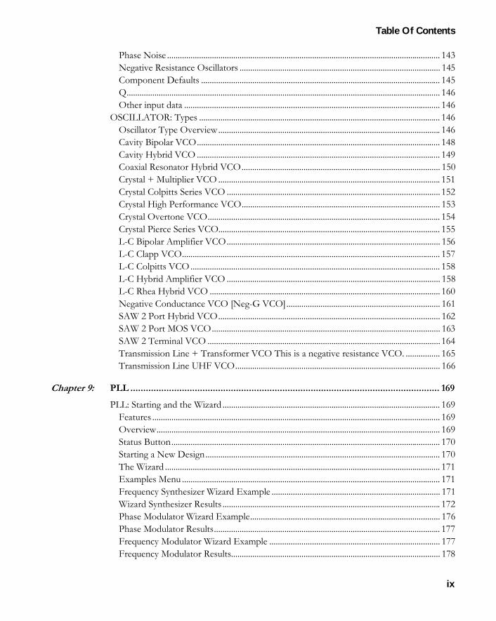
Table Of Contents
ix
Phase Noise ................................................................................................................................ 143 Negative Resistance Oscillators .............................................................................................. 145 Component Defaults ................................................................................................................ 145 Q................................................................................................................................................... 146 Other input data ........................................................................................................................ 146
OSCILLATOR: Types ................................................................................................................. 146 Oscillator Type Overview........................................................................................................ 146 Cavity Bipolar VCO.................................................................................................................. 148 Cavity Hybrid VCO .................................................................................................................. 149 Coaxial Resonator Hybrid VCO............................................................................................. 150 Crystal + Multiplier VCO ........................................................................................................ 151 Crystal Colpitts Series VCO .................................................................................................... 152 Crystal High Performance VCO............................................................................................. 153 Crystal Overtone VCO............................................................................................................. 154 Crystal Pierce Series VCO........................................................................................................ 155 L-C Bipolar Amplifier VCO.................................................................................................... 156 L-C Clapp VCO......................................................................................................................... 157 L-C Colpitts VCO ..................................................................................................................... 158 L-C Hybrid Amplifier VCO .................................................................................................... 158 L-C Rhea Hybrid VCO ............................................................................................................ 160 Negative Conductance VCO [Neg-G VCO]........................................................................ 161 SAW 2 Port Hybrid VCO........................................................................................................ 162 SAW 2 Port MOS VCO........................................................................................................... 163 SAW 2 Terminal VCO ............................................................................................................. 164 Transmission Line + Transformer VCO This is a negative resistance VCO. ................ 165 Transmission Line UHF VCO................................................................................................ 166
Chapter 9: PLL ........................................................................................................................ 169
PLL: Starting and the Wizard ...................................................................................................... 169 Features ....................................................................................................................................... 169 Overview..................................................................................................................................... 169 Status Button.............................................................................................................................. 170 Starting a New Design.............................................................................................................. 170 The Wizard ................................................................................................................................. 171 Examples Menu ......................................................................................................................... 171 Frequency Synthesizer Wizard Example ............................................................................... 171 Wizard Synthesizer Results ...................................................................................................... 172 Phase Modulator Wizard Example......................................................................................... 176 Phase Modulator Results.......................................................................................................... 177 Frequency Modulator Wizard Example ................................................................................ 177 Frequency Modulator Results.................................................................................................. 178
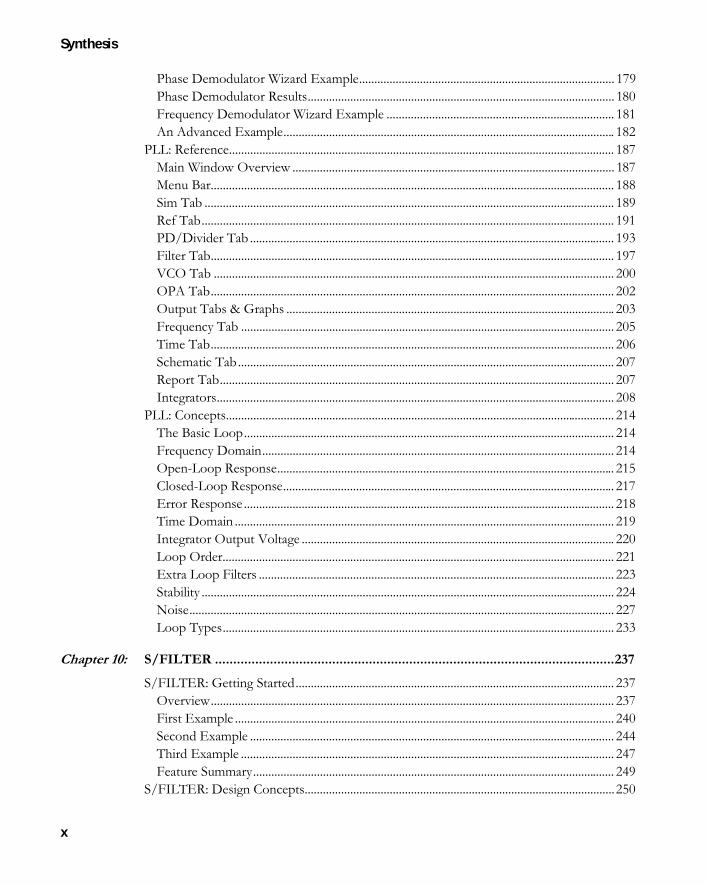
Synthesis
x
Phase Demodulator Wizard Example.................................................................................... 179 Phase Demodulator Results..................................................................................................... 180 Frequency Demodulator Wizard Example ........................................................................... 181 An Advanced Example............................................................................................................. 182
PLL: Reference............................................................................................................................... 187 Main Window Overview .......................................................................................................... 187 Menu Bar..................................................................................................................................... 188 Sim Tab ....................................................................................................................................... 189 Ref Tab........................................................................................................................................ 191 PD/Divider Tab ........................................................................................................................ 193 Filter Tab..................................................................................................................................... 197 VCO Tab .................................................................................................................................... 200 OPA Tab..................................................................................................................................... 202 Output Tabs & Graphs ............................................................................................................ 203 Frequency Tab ........................................................................................................................... 205 Time Tab..................................................................................................................................... 206 Schematic Tab............................................................................................................................ 207 Report Tab.................................................................................................................................. 207 Integrators................................................................................................................................... 208
PLL: Concepts................................................................................................................................ 214 The Basic Loop.......................................................................................................................... 214 Frequency Domain.................................................................................................................... 214 Open-Loop Response............................................................................................................... 215 Closed-Loop Response............................................................................................................. 217 Error Response .......................................................................................................................... 218 Time Domain ............................................................................................................................. 219 Integrator Output Voltage ....................................................................................................... 220 Loop Order................................................................................................................................. 221 Extra Loop Filters ..................................................................................................................... 223 Stability ........................................................................................................................................ 224 Noise............................................................................................................................................ 227 Loop Types................................................................................................................................. 233
Chapter 10: S/FILTER .............................................................................................................237
S/FILTER: Getting Started......................................................................................................... 237 Overview..................................................................................................................................... 237 First Example ............................................................................................................................. 240 Second Example ........................................................................................................................ 244 Third Example ........................................................................................................................... 247 Feature Summary....................................................................................................................... 249
S/FILTER: Design Concepts......................................................................................................250
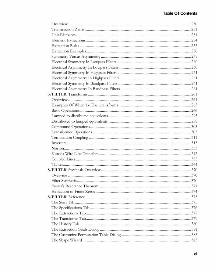
Table Of Contents
xi
Overview..................................................................................................................................... 250 Transmission Zeros................................................................................................................... 251 Unit Elements ............................................................................................................................ 251 Element Extractions ................................................................................................................. 254 Extraction Rules ........................................................................................................................ 255 Extraction Examples................................................................................................................. 256 Symmetry Versus Asymmetry ................................................................................................. 259 Electrical Symmetry In Lowpass Filters ................................................................................ 260 Electrical Asymmetry In Lowpass Filters.............................................................................. 260 Electrical Symmetry In Highpass Filters ............................................................................... 261 Electrical Asymmetry In Highpass Filters............................................................................. 261 Electrical Symmetry In Bandpass Filters............................................................................... 261 Electrical Asymmetry In Bandpass Filters ............................................................................ 261
S/FILTER: Transforms ............................................................................................................... 261 Overview..................................................................................................................................... 261 Examples Of When To Use Transforms .............................................................................. 263 Basic Operations........................................................................................................................ 266 Lumped to distributed equivalents ......................................................................................... 293 Distributed to lumped equivalents ......................................................................................... 298 Compound Operations............................................................................................................. 303 Transformer Operations .......................................................................................................... 305 Termination Coupling .............................................................................................................. 311 Inverters ...................................................................................................................................... 315 Norton......................................................................................................................................... 333 Kuroda Wire Line Transfers.................................................................................................... 342 Coupled Lines ............................................................................................................................ 355 TLines.......................................................................................................................................... 364
S/FILTER: Synthesis Overview................................................................................................. 370 Overview..................................................................................................................................... 370 Filter Synthesis ........................................................................................................................... 370 Foster's Reactance Theorem.................................................................................................... 371 Extraction of Finite Zeros ....................................................................................................... 374
S/FILTER: Reference .................................................................................................................. 375 The Start Tab ............................................................................................................................. 375 The Specifications Tab ............................................................................................................. 376 The Extractions Tab ................................................................................................................. 377 The Transforms Tab................................................................................................................. 379 The History Tab ........................................................................................................................ 380 The Extraction Goals Dialog .................................................................................................. 381 The Customize Permutation Table Dialog ........................................................................... 383 The Shape Wizard ..................................................................................................................... 385

Synthesis
xii
Chapter 11: Signal Control.........................................................................................................389
Signal Control: Operation ............................................................................................................ 389 Signal Control Overview .......................................................................................................... 389
Signal Control: Types.................................................................................................................... 399 Overview..................................................................................................................................... 399
Chapter 12: TLINE ...................................................................................................................419
Overview......................................................................................................................................... 419 Standalone Operation ................................................................................................................... 419
Starting TLINE.......................................................................................................................... 419 Screen Layout............................................................................................................................. 420 Operation.................................................................................................................................... 422 Example ...................................................................................................................................... 423 Synthesizing Dimensions ......................................................................................................... 424 Outputs ....................................................................................................................................... 424 Changing Input Parameters ..................................................................................................... 425 Units............................................................................................................................................. 426 Automatic Defaults ................................................................................................................... 426 Input Parameter Ranges ........................................................................................................... 426
Advanced TLINE Operation ...................................................................................................... 426 Overview..................................................................................................................................... 426 Advanced TLINE Example..................................................................................................... 426 Advanced TLINE...................................................................................................................... 435
Calculations..................................................................................................................................... 436 Overview..................................................................................................................................... 436 Accuracy...................................................................................................................................... 436 Input Parameters ....................................................................................................................... 437 Output Parameters .................................................................................................................... 437 Effective Dielectric Constant ..................................................................................................438 Loss.............................................................................................................................................. 438 Propagation Velocity................................................................................................................. 439 Highest Frequency..................................................................................................................... 439 Cover ........................................................................................................................................... 439 Resonator Q ............................................................................................................................... 440 Coupling...................................................................................................................................... 440
Chapter 13: WhatIF Frequency Planner....................................................................................441
WhatIF Overview.......................................................................................................................... 441 WhatIF Background...................................................................................................................... 442 Spur Analysis Basics ...................................................................................................................... 442 Traditional Approaches ................................................................................................................ 442
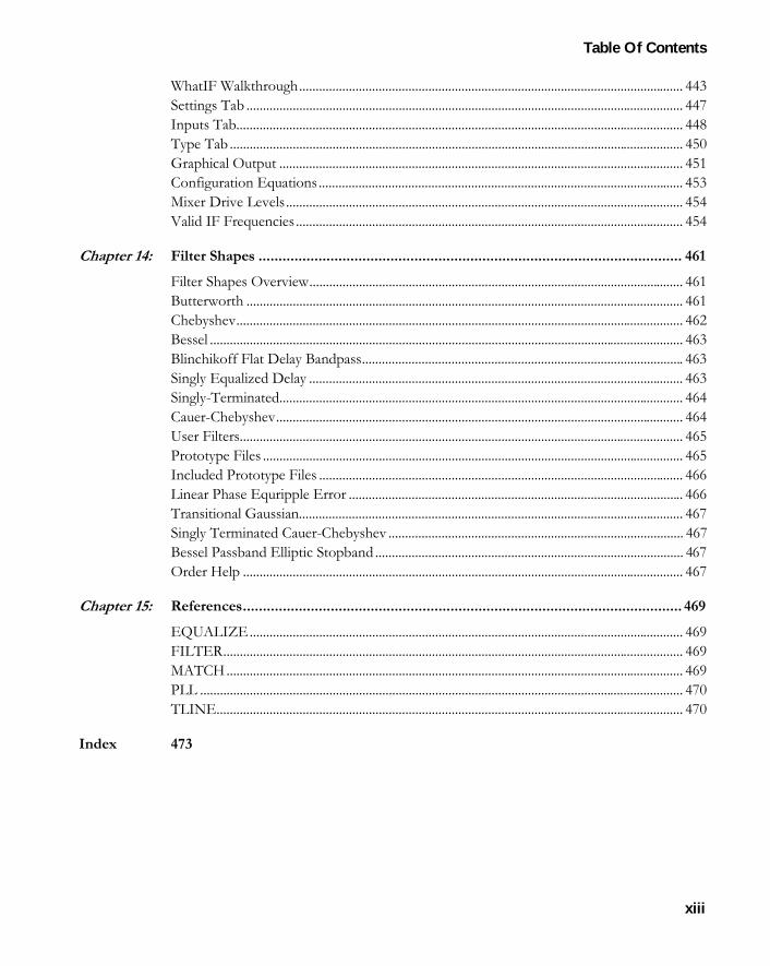
Table Of Contents
xiii
WhatIF Walkthrough.................................................................................................................... 443 Settings Tab .................................................................................................................................... 447 Inputs Tab....................................................................................................................................... 448 Type Tab ......................................................................................................................................... 450 Graphical Output .......................................................................................................................... 451 Configuration Equations.............................................................................................................. 453 Mixer Drive Levels........................................................................................................................ 454 Valid IF Frequencies ..................................................................................................................... 454
Chapter 14: Filter Shapes .......................................................................................................... 461
Filter Shapes Overview................................................................................................................. 461 Butterworth .................................................................................................................................... 461 Chebyshev....................................................................................................................................... 462 Bessel ............................................................................................................................................... 463 Blinchikoff Flat Delay Bandpass................................................................................................. 463 Singly Equalized Delay ................................................................................................................. 463 Singly-Terminated.......................................................................................................................... 464 Cauer-Chebyshev........................................................................................................................... 464 User Filters...................................................................................................................................... 465 Prototype Files ............................................................................................................................... 465 Included Prototype Files .............................................................................................................. 466 Linear Phase Equripple Error ..................................................................................................... 466 Transitional Gaussian.................................................................................................................... 467 Singly Terminated Cauer-Chebyshev ......................................................................................... 467 Bessel Passband Elliptic Stopband ............................................................................................. 467 Order Help ..................................................................................................................................... 467
Chapter 15: References.............................................................................................................. 469
EQUALIZE................................................................................................................................... 469 FILTER........................................................................................................................................... 469 MATCH.......................................................................................................................................... 469 PLL .................................................................................................................................................. 470 TLINE............................................................................................................................................. 470
Index 473


1
Chapter 1: Introduction
Overview For system requirements, installation, and setup information, refer to the Installation manual. This manual (Synthesis) describes FILTER, M/FILTER, A/FILTER, EQUALIZE, MATCH, OSCILLATOR, PLL, S/FILTER, and TLINE.
Only walkthrough examples are in this manual. Complete practical examples can now be found in the Examples manual.


3
Chapter 2: A/FILTER
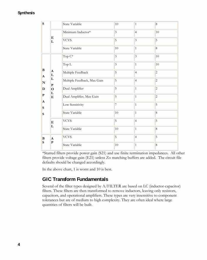
A/FILTER: Types
Overview Filter type specifies whether the filter is lowpass, highpass, bandpass, or bandstop. For each type, A/FILTER offers several available topologies. Each of these has different options and benefits, depending on the application need. Schematics and descriptions of the topologies designed by A/FILTER are given on the following pages.
Refer to the Filter Shapes section for a discussion of filter transfer approximations (shapes).
Filter Type Tunability Simplicity Insensitivity
Minimum Inductor 3 3 10
Minimum Capacitor 3 4 10
Single Feedback 5 6 2
Multiple Feedback 5 5 2
Low Sensitivity 7 3 5
VCVS 5 3 5
A L L
P O L E
State Variable 10 1 8
Minimum Capacitor 3 4 10
VCVS 5 4 5
L
O
W
P
A
S
S
E L
State Variable 10 1 8
Minimum Inductor 3 4 10
Minimum Capacitor 3 3 10
Single Feedback 5 6 2
Multiple Feedback 5 5 2
Low Sensitivity 7 3 5
H
I
G
H
P
A
S
A L L
P O L E
VCVS 5 3 5
Synthesis
4
State Variable 10 1 8
Minimum Inductor* 3 4 10
VCVS 5 3 5
S
E L
State Variable 10 1 8
Top C* 3 3 10
Top L 3 1 10
Multiple Feedback 5 4 2
Multiple Feedback, Max Gain 5 4 2
Dual Amplifier 5 1 2
Dual Amplifier, Max Gain 5 1 2
Low Sensitivity 7 1 5
A L L
P O L E
State Variable 10 1 8
VCVS 5 4 5
B
A
N
D
P
A
S
S
E L
State Variable 10 1 8
VCVS 5 4 5 B S
A P
State Variable 10 1 8
*Starred filters provide power gain (S21) and use finite termination impedances. All other filters provide voltage gain (E21) unless Zo matching buffers are added. The circuit file defaults should be changed accordingly.
In the above chart, 1 is worst and 10 is best.
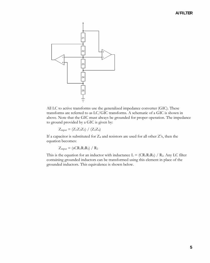
GIC Transform Fundamentals Several of the filter types designed by A/FILTER are based on LC (inductor-capacitor) filters. These filters are then transformed to remove inductors, leaving only resistors, capacitors, and operational amplifiers. These types are very insensitive to component tolerances but are of medium to high complexity. They are often ideal where large quantities of filters will be built.
A/FILTER
5
All LC to active transforms use the generalized impedance converter (GIC). These transforms are referred to as LC/GIC transforms. A schematic of a GIC is shown in above. Note that the GIC must always be grounded for proper operation. The impedance to ground provided by a GIC is given by:
Zinput = (Z1Z3Z5) / (Z2Z4)
If a capacitor is substituted for Z4 and resistors are used for all other Z’s, then the equation becomes:
Zinput = (sCR1R3R5) / R2
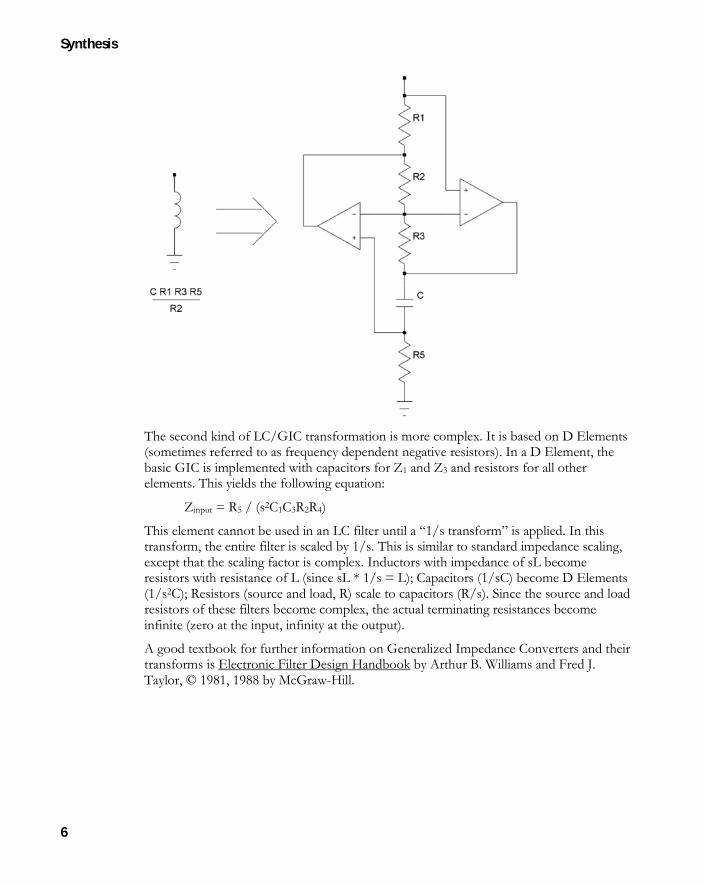
This is the equation for an inductor with inductance L = (CR1R3R5) / R2. Any LC filter containing grounded inductors can be transformed using this element in place of the grounded inductors. This equivalence is shown below.
Synthesis
6
The second kind of LC/GIC transformation is more complex. It is based on D Elements (sometimes referred to as frequency dependent negative resistors). In a D Element, the basic GIC is implemented with capacitors for Z1 and Z3 and resistors for all other elements. This yields the following equation:
Zinput = R5 / (s2C1C3R2R4)
This element cannot be used in an LC filter until a “1/s transform” is applied. In this transform, the entire filter is scaled by 1/s. This is similar to standard impedance scaling, except that the scaling factor is complex. Inductors with impedance of sL become resistors with resistance of L (since sL * 1/s = L); Capacitors (1/sC) become D Elements (1/s2C); Resistors (source and load, R) scale to capacitors (R/s). Since the source and load resistors of these filters become complex, the actual terminating resistances become infinite (zero at the input, infinity at the output).
A good textbook for further information on Generalized Impedance Converters and their transforms is Electronic Filter Design Handbook by Arthur B. Williams and Fred J. Taylor, © 1981, 1988 by McGraw-Hill.
A/FILTER
7
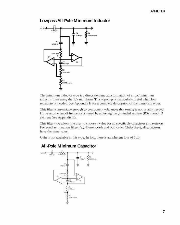
Lowpass All-Pole Minimum Inductor
The minimum inductor type is a direct element transformation of an LC minimum inductor filter using the 1/s transform. This topology is particularly useful when low sensitivity is needed. See Appendix E for a complete description of the transform types.
This filter is insensitive enough to component tolerances that tuning is not usually needed. However, the cutoff frequency is tuned by adjusting the grounded resistor (R3) in each D element (see Appendix E).
This filter type allows the user to choose a value for all specifiable capacitors and resistors. For equal termination filters (e.g. Butterworth and odd-order Chebyshev), all capacitors have the same value.
Gain is not available in this type. In fact, there is an inherent loss of 6dB.
All-Pole Minimum Capacitor
Synthesis
8
This type is a direct transform of the LC minimum capacitor filter using the 1/s transform. For odd order filters, there are fewer D elements in this type than in a comparable minimum inductor filter. However, there are more resistors in series with the signal path in this type. See Appendix E for a complete discussion of GIC transforms.
The minimum capacitor filter is tuned exactly as the minimum inductor type. Resistor R4 in the schematic tunes the cutoff frequency of the response.
This filter type allows the user to choose a value for all specifiable capacitors and resistors. For equal termination filters (e.g. Butterworth and odd-order Chebyshev), all capacitors have the same value.
Gain is not available in this type, and there is an inherent loss of 6dB.
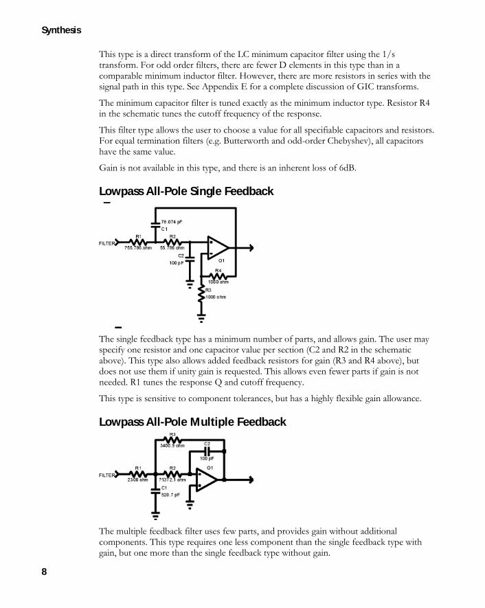
Lowpass All-Pole Single Feedback
The single feedback type has a minimum number of parts, and allows gain. The user may specify one resistor and one capacitor value per section (C2 and R2 in the schematic above). This type also allows added feedback resistors for gain (R3 and R4 above), but does not use them if unity gain is requested. This allows even fewer parts if gain is not needed. R1 tunes the response Q and cutoff frequency.
This type is sensitive to component tolerances, but has a highly flexible gain allowance.
Lowpass All-Pole Multiple Feedback
The multiple feedback filter uses few parts, and provides gain without additional components. This type requires one less component than the single feedback type with gain, but one more than the single feedback type without gain.
A/FILTER
9
One capacitor value per section is selected arbitrarily (C2 in the schematic above). Resistor R2 in the schematic tunes the Q and cutoff frequency of the filter.
This type has a high sensitivity to component tolerances.
Lowpass All-Pole Low Sensitivity
The low sensitivity realization uses two op-amps per pole pair, but has a low sensitivity to the op-amp open loop gain.
This topology allows two capacitors per section (C1 and C2 in the schematic) to be chosen. Resistor R1 on the schematic is used to tune the response. This type has a low sensitivity to differences in op-amp open loop gain between sections, but requires the two amplifiers within each section to have similar characteristics. Usually, op-amps on a dual or quad package will have closely matched, if not identical operating parameters.
This topology does not allow gain.
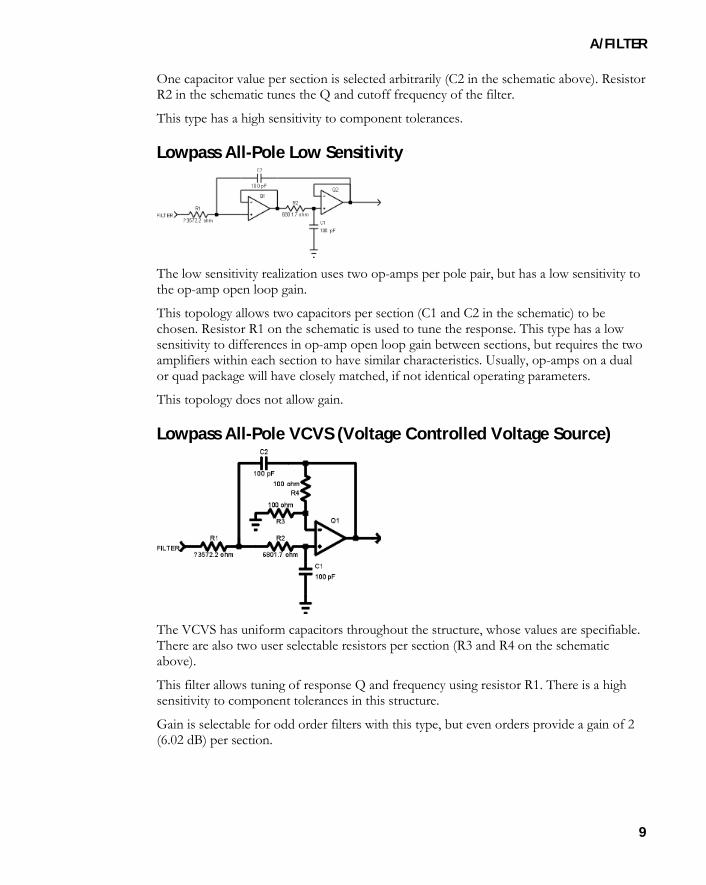
Lowpass All-Pole VCVS (Voltage Controlled Voltage Source)
The VCVS has uniform capacitors throughout the structure, whose values are specifiable. There are also two user selectable resistors per section (R3 and R4 on the schematic above).
This filter allows tuning of response Q and frequency using resistor R1. There is a high sensitivity to component tolerances in this structure.
Gain is selectable for odd order filters with this type, but even orders provide a gain of 2 (6.02 dB) per section.

Synthesis
10
Lowpass All-Pole State Variable (Biquad)
The state variable filter is best known for its tunability. This type contains many parts per section, but every aspect of the filter response is tuned directly. This gives a large degree of freedom for component tolerances.
This type also exhibits low sensitivity to operational amplifier characteristics, such as narrow bandwidth and open-loop gain.
The state variable structure allows user specifiable uniform capacitors throughout the entire circuit as well as two resistors per section (R3 and R4 in the above schematic).
For tuning, refer to the above schematic:
1. Adjust R5 for correct cutoff frequency
2. Adjust R6 for desired Q
3. Adjust R1 for overall gain desired
Lowpass Elliptic Minimum Capacitor
The minimum capacitor elliptic type uses a 1/s transformation. See Appendix E for a complete discussion of the transform types.
A/FILTER
11
This filter is tuned by adjusting the grounded resistor (R5) in each D element (see Appendix E). The zero frequency is tuned by using R2 in the schematic above.
This topology has a very low sensitivity to component tolerances, and a loss of 6dB within the filter passband.
Note: This filter provides power gain, rather than voltage gain. This means that S21 should be displayed, rather than E21.
Gain is not available with this topology.
Lowpass Elliptic VCVS
The VCVS uses user selected capacitors throughout the structure. There is also one user selectable resistor per section (R5 on the above schematic).
This type has a low sensitivity to component tolerances, and does not usually require tuning, however the filter is tuned using the resistors R1 and R4 shown on the schematic above.
This filter type produces gain, but does not allow its specification by the user.
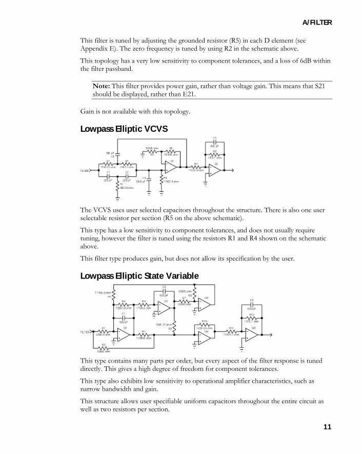
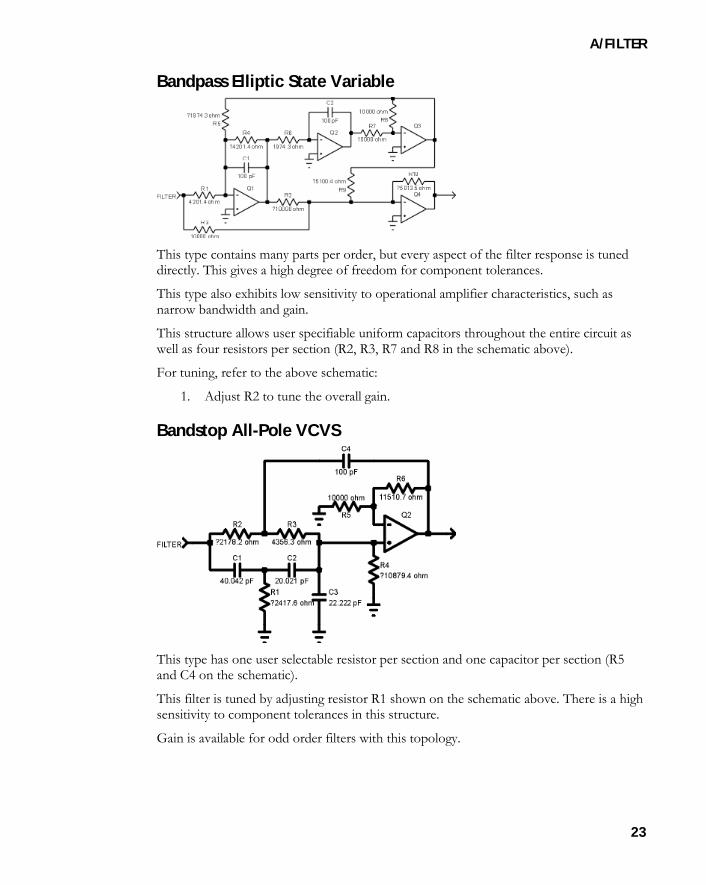
Lowpass Elliptic State Variable
This type contains many parts per order, but every aspect of the filter response is tuned directly. This gives a high degree of freedom for component tolerances.
This type also exhibits low sensitivity to operational amplifier characteristics, such as narrow bandwidth and gain.
This structure allows user specifiable uniform capacitors throughout the entire circuit as well as two resistors per section.
Synthesis
12
For tuning, refer to the above schematic:
1. R6 tunes the cutoff frequency, and the zero frequency.
2. R2 tunes the quality of the zero.
3. R4 tunes the response Q.
4. R5 tunes the passband gain.
5. R10 tunes the overall gain.
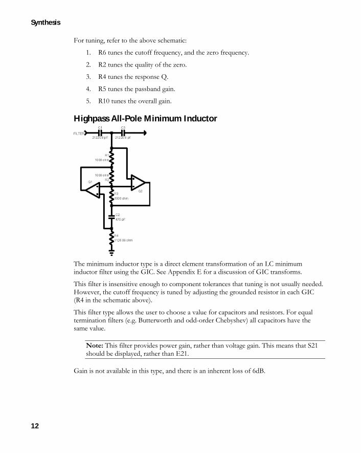
Highpass All-Pole Minimum Inductor
The minimum inductor type is a direct element transformation of an LC minimum inductor filter using the GIC. See Appendix E for a discussion of GIC transforms.
This filter is insensitive enough to component tolerances that tuning is not usually needed. However, the cutoff frequency is tuned by adjusting the grounded resistor in each GIC (R4 in the schematic above).
This filter type allows the user to choose a value for capacitors and resistors. For equal termination filters (e.g. Butterworth and odd-order Chebyshev) all capacitors have the same value.
Note: This filter provides power gain, rather than voltage gain. This means that S21 should be displayed, rather than E21.
Gain is not available in this type, and there is an inherent loss of 6dB.
A/FILTER
13
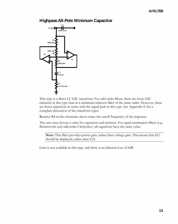
Highpass All-Pole Minimum Capacitor
This type is a direct LC GIC transform. For odd order filters, there are more GIC elements in this type than in a minimum inductor filter of the same order. However, there are fewer capacitors in series with the signal path in this type. See Appendix E for a complete discussion of the transform types.
Resistor R4 in the schematic above tunes the cutoff frequency of the response.
The user may choose a value for capacitors and resistors. For equal termination filters (e.g. Butterworth and odd-order Chebyshev) all capacitors have the same value.
Note: This filter provides power gain, rather than voltage gain. This means that S21 should be displayed, rather than E21.
Gain is not available in this type, and there is an inherent loss of 6dB.
Synthesis
14
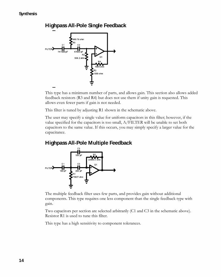
Highpass All-Pole Single Feedback
This type has a minimum number of parts, and allows gain. This section also allows added feedback resistors (R3 and R4) but does not use them if unity gain is requested. This allows even fewer parts if gain is not needed.
This filter is tuned by adjusting R1 shown in the schematic above.
The user may specify a single value for uniform capacitors in this filter; however, if the value specified for the capacitors is too small, A/FILTER will be unable to set both capacitors to the same value. If this occurs, you may simply specify a larger value for the capacitance.
Highpass All-Pole Multiple Feedback
The multiple feedback filter uses few parts, and provides gain without additional components. This type requires one less component than the single feedback type with gain.
Two capacitors per section are selected arbitrarily (C1 and C3 in the schematic above). Resistor R1 is used to tune this filter.
This type has a high sensitivity to component tolerances.
A/FILTER
15
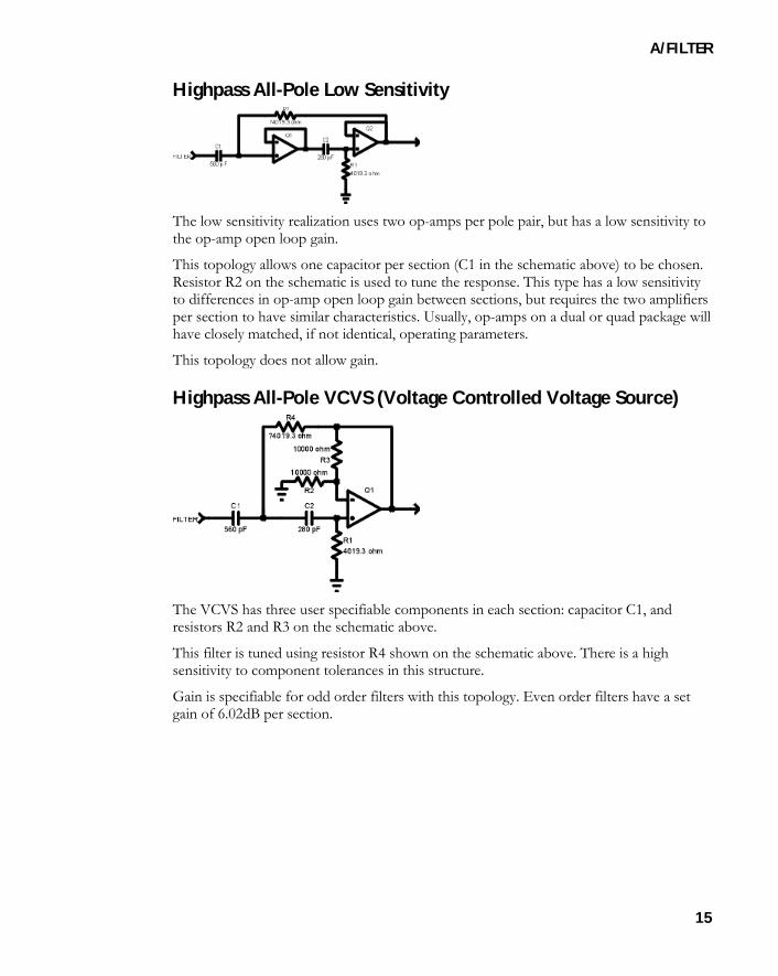
Highpass All-Pole Low Sensitivity
The low sensitivity realization uses two op-amps per pole pair, but has a low sensitivity to the op-amp open loop gain.
This topology allows one capacitor per section (C1 in the schematic above) to be chosen. Resistor R2 on the schematic is used to tune the response. This type has a low sensitivity to differences in op-amp open loop gain between sections, but requires the two amplifiers per section to have similar characteristics. Usually, op-amps on a dual or quad package will have closely matched, if not identical, operating parameters.
This topology does not allow gain.
Highpass All-Pole VCVS (Voltage Controlled Voltage Source)
The VCVS has three user specifiable components in each section: capacitor C1, and resistors R2 and R3 on the schematic above.
This filter is tuned using resistor R4 shown on the schematic above. There is a high sensitivity to component tolerances in this structure.
Gain is specifiable for odd order filters with this topology. Even order filters have a set gain of 6.02dB per section.
Synthesis
16
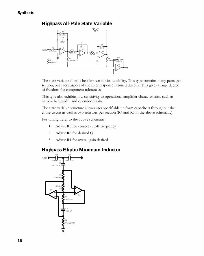
Highpass All-Pole State Variable
The state variable filter is best known for its tunability. This type contains many parts per section, but every aspect of the filter response is tuned directly. This gives a large degree of freedom for component tolerances.
This type also exhibits low sensitivity to operational amplifier characteristics, such as narrow bandwidth and open-loop gain.
The state variable structure allows user specifiable uniform capacitors throughout the entire circuit as well as two resistors per section (R4 and R5 in the above schematic).
For tuning, refer to the above schematic:
1. Adjust R5 for correct cutoff frequency
2. Adjust R6 for desired Q
3. Adjust R1 for overall gain desired
Highpass Elliptic Minimum Inductor
A/FILTER
17
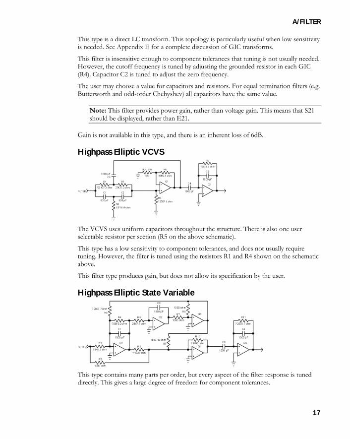
This type is a direct LC transform. This topology is particularly useful when low sensitivity is needed. See Appendix E for a complete discussion of GIC transforms.
This filter is insensitive enough to component tolerances that tuning is not usually needed. However, the cutoff frequency is tuned by adjusting the grounded resistor in each GIC (R4). Capacitor C2 is tuned to adjust the zero frequency.
The user may choose a value for capacitors and resistors. For equal termination filters (e.g. Butterworth and odd-order Chebyshev) all capacitors have the same value.
Note: This filter provides power gain, rather than voltage gain. This means that S21 should be displayed, rather than E21.
Gain is not available in this type, and there is an inherent loss of 6dB.
Highpass Elliptic VCVS
The VCVS uses uniform capacitors throughout the structure. There is also one user selectable resistor per section (R5 on the above schematic).
This type has a low sensitivity to component tolerances, and does not usually require tuning. However, the filter is tuned using the resistors R1 and R4 shown on the schematic above.
This filter type produces gain, but does not allow its specification by the user.
Highpass Elliptic State Variable
This type contains many parts per order, but every aspect of the filter response is tuned directly. This gives a large degree of freedom for component tolerances.
Synthesis
18
This type also exhibits low sensitivity to operational amplifier characteristics, such as narrow bandwidth and gain.
This structure allows user specifiable uniform capacitors throughout the entire circuit as well as five resistors per section (R2, R4, R5, R6 and R10 in the schematic above).
For tuning, refer to the above schematic:
1. R6 tunes the cutoff frequency, and the zero frequency.
2. R2 tunes the quality of the zero.
3. R4 tunes the response Q.
4. R5 tunes the passband gain.
5. R10 tunes the overall gain.
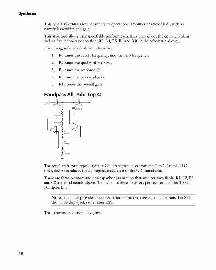
Bandpass All-Pole Top C
The top C transform type is a direct GIC transformation from the Top C Coupled LC filter. See Appendix E for a complete discussion of the GIC transform.
There are three resistors and one capacitor per section that are user specifiable: R1, R2, R3 and C2 in the schematic above. This type has fewer resistors per section than the Top L Bandpass filter.
Note: This filter provides power gain, rather than voltage gain. This means that S21 should be displayed, rather than E21.
This structure does not allow gain.

A/FILTER
19
Bandpass All-Pole Top L
The top L transform type is a direct GIC transformation from the Top L Coupled LC filter. See Appendix E for a complete discussion of the transform types.
There are three specifiable capacitors and two resistors per section: C1, C2, C3, R3 and R4 in the above schematic. This type has fewer capacitors per section than the Top C Bandpass filter. For equal termination filters (e.g. Butterworth and odd-order Chebyshev) all capacitors have the same value.
This structure does not allow gain, and there is an inherent loss of 6dB.
Bandpass All-Pole Multiple Feedback
The multiple feedback filter uses few parts, and provides gain without additional components. This type requires fewer components than the single feedback type with gain, but more than the single feedback type without gain.
One value is user specified for uniform capacitors within this filter.
This type has a high sensitivity to component tolerances. For tuning, refer to the above schematic:
1. Adjust R2 and R3 for the correct cutoff frequencies
2. Adjust R1 for the desired gain
Synthesis
20
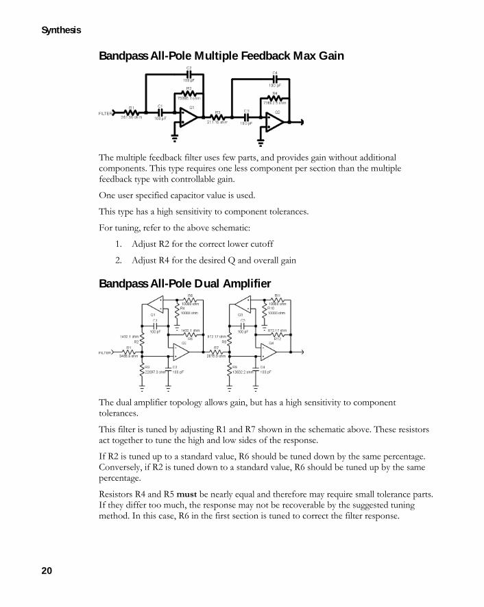
Bandpass All-Pole Multiple Feedback Max Gain
The multiple feedback filter uses few parts, and provides gain without additional components. This type requires one less component per section than the multiple feedback type with controllable gain.
One user specified capacitor value is used.
This type has a high sensitivity to component tolerances.
For tuning, refer to the above schematic:
1. Adjust R2 for the correct lower cutoff
2. Adjust R4 for the desired Q and overall gain
Bandpass All-Pole Dual Amplifier
The dual amplifier topology allows gain, but has a high sensitivity to component tolerances.
This filter is tuned by adjusting R1 and R7 shown in the schematic above. These resistors act together to tune the high and low sides of the response.
If R2 is tuned up to a standard value, R6 should be tuned down by the same percentage. Conversely, if R2 is tuned down to a standard value, R6 should be tuned up by the same percentage.
Resistors R4 and R5 must be nearly equal and therefore may require small tolerance parts. If they differ too much, the response may not be recoverable by the suggested tuning method. In this case, R6 in the first section is tuned to correct the filter response.

A/FILTER
21
Bandpass All-Pole Dual Amplifier Max Gain
The dual amplifier maximum gain type requires one less resistor per section than the standard dual amplifier filter. This topology allows gain, but has a high sensitivity to component tolerances.
This filter is tuned by adjusting R1 and R6 shown in the schematic above. In general, the bandpass types exhibit symmetry.
Within each stage, if resistors R2 and R5 in the schematic above are to be set to standard values, one should be tuned up while the other is tuned down. This will correctly adjust the response.
If R3 and R4 differ in the constructed filter, the response may not be recoverable by the suggested tuning method. In this case, R6 in the first section is tuned to correct the filter response.
Bandpass All-Pole Low Sensitivity
This type has a low sensitivity to op-amp characteristics. It uses generalized impedance converters, and exhibits better behavior at high frequencies than the dual amplifier type. However, it requires one more op-amp per section. This type has a low sensitivity to differences in op-amp open loop gain between GIC sections, but requires the two amplifiers per section to have similar characteristics. Usually, op-amps on a dual or quad package will have closely matched operating parameters.
Synthesis
22
This filter is tuned by adjusting the grounded resistor in each section (R5 in the above schematic).
Gain is allowed in this filter.
Bandpass All-Pole State Variable
The state variable filter is best known for its tunability. This type contains many parts per section, but every aspect of the filter response is tuned directly. This gives a high degree of freedom for component tolerances.
This type also exhibits low sensitivity to operational amplifier characteristics, such as narrow bandwidth and open-loop gain.
The state variable structure allows user specifiable uniform capacitors throughout the circuit as well as two resistors per section (R3 and R4 in the above schematic).
For tuning, refer to the above schematic:
1. Adjust R6 for correct cutoff frequency
2. Adjust R5 for desired Q
3. Adjust R1 for overall gain desired
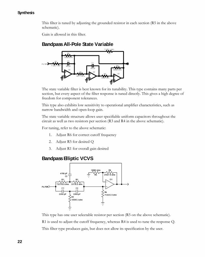
Bandpass Elliptic VCVS
This type has one user selectable resistor per section (R5 on the above schematic).
R1 is used to adjust the cutoff frequency, whereas R4 is used to tune the response Q.
This filter type produces gain, but does not allow its specification by the user.
A/FILTER
23
Bandpass Elliptic State Variable
This type contains many parts per order, but every aspect of the filter response is tuned directly. This gives a high degree of freedom for component tolerances.
This type also exhibits low sensitivity to operational amplifier characteristics, such as narrow bandwidth and gain.
This structure allows user specifiable uniform capacitors throughout the entire circuit as well as four resistors per section (R2, R3, R7 and R8 in the schematic above).
For tuning, refer to the above schematic:
1. Adjust R2 to tune the overall gain.
Bandstop All-Pole VCVS
This type has one user selectable resistor per section and one capacitor per section (R5 and C4 on the schematic).
This filter is tuned by adjusting resistor R1 shown on the schematic above. There is a high sensitivity to component tolerances in this structure.
Gain is available for odd order filters with this topology.

Synthesis
24
Bandstop All-Pole State Variable
The state variable filter is best known for its tunability. This type contains many parts per section, but every aspect of the filter response is tuned directly. This gives a high degree of freedom for component tolerances.
This type also exhibits low sensitivity to operational amplifier characteristics, such as narrow bandwidth and open-loop gain.
The state variable structure allows user specifiable uniform capacitors throughout the entire circuit as well as four resistors per section (R2, R3, R7 and R8 in the above schematic).
For tuning, refer to the above schematic:
1. Adjust R5 and R9 for the correct zero frequency
2. Adjust R4 for desired Q
3. Adjust R10 for desired overall gain
A/FILTER: Operation
Active Filter Synthesis Overview A/FILTER makes designing active filters fast and easy. A/FILTER also includes EQUALIZE for active equalizer synthesis. With a GENESYS simulator, you can simulate the filter performance, customize or optimize the filter, and check the effects of parasitic reactances or finite op-amp parameters, such as unity gain bandwidth.
Note: Several A/FILTER examples with measured results are presented in the Filters section of the Examples manual.
A/FILTER synthesizes many filter types suitable for a wide range of applications. Principle features include:
• Over 30 filter topologies. Choices provide for practical realization of specific application needs. Many types allow specification of passband gain.
• A wide range of transfer approximations (amplitude, phase and delay response shapes).
A/FILTER
25
• Effective noise bandwidth calculation
• Full integration with GENESYS Environment
Walkthrough The first design example will be a Single Feedback 7th order lowpass filter with a 0.25 dB passband ripple Chebyshev response. The cutoff frequency is 10 kHz and the filter will have +2dB gain in the passband.
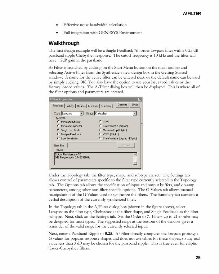
A/Filter is launched by clicking on the Start Menu button on the main toolbar and selecting Active Filter from the Synthesize a new design box in the Getting Started window. A name for the active filter can be entered next, or the default name can be used by simply clicking OK. You also have the option to use your last saved values or the factory loaded values. The A/Filter dialog box will then be displayed. This is where all of the filter options and parameters are entered.
Under the Topology tab, the filter type, shape, and subtype are set. The Settings tab allows control of parameters specific to the filter type currently selected in the Topology tab. The Options tab allows the specification of input and output buffers, and op-amp parameters, among other non-filter-specific options. The G Values tab allows manual manipulation of the G Values used to synthesize the filters. The Summary tab contains a verbal description of the currently synthesized filter.
In the Topology tab in the A/Filter dialog box (shown in the figure above), select Lowpass as the filter type, Chebyshev as the filter shape, and Single Feedback as the filter subtype. Next, click on the Settings tab. Set the Order to 7. Filters up to 21st order may be designed for most types. The suggested range at the bottom of the window gives a reminder of the valid range for the currently selected input.
Next, enter a Passband Ripple of 0.25. A/Filter directly computes the lowpass prototype G values for popular response shapes and does not use tables for these shapes, so any real value less than 3 dB may be chosen for the passband ripple. This is true even for elliptic Cauer-Chebyshev filters.

Synthesis
26
The cutoff frequency of all-pole filters, such as Butterworth, is normally defined as the 3 dB attenuation frequency. The cutoff of filters with ripple in the passband, such as Chebyshev, is often defined as the ripple value. A/Filter allows specification of the attenuation at the cutoff frequency for Butterworth and Chebyshev filters. For normally defined cutoff attenuation, enter the Attenuation at Cutoff equal to the ripple value for Chebyshev filters, and 3.01 dB for Butterworth filters.
For this example, enter 0.25 for the Attenuation at Cutoff.
Next, for Butterworth and Chebyshev filters, A/Filter prompts for the Cutoff Frequency, i.e. the frequency at which the specified cutoff attenuation will occur.
Enter 0.01 for the Cutoff Frequency. Cutoff Frequency must be specified in MHz, and 0.01 MHz = 10 kHz.
The Resonator R is the desired value for the selectable resistors in the current filter. Resonator C is the desired value of capacitance. Certain filter types allow the user to specify one or more part values. When this is the case, A/Filter prompts for the value. This can be any valid part value. Not all of the part values are selectable. Some filter types allow selection of resistors, whereas some do not allow any freedom. This is discussed in further detail in the A/Filter Types section.
For this example, enter 10000 for the Resonator R value, and 10000 for the Resonator C value.
The schematic of the filter is shown in the schematic window as it is below.
Parameters
Options Most of the filter topologies designed by A/FILTER use a minimum number of components, and do not match to a specified source or load termination. For this reason, the transmission and reflection parameters may behave erratically unless a matching buffer is added at either end. For instance, the Minimum Inductor and Minimum Capacitor types assume a near zero source termination, and near infinite load resistance.
Unless low or high values are specified for the source and load terminations (A/FILTER default) the source sees a mismatch and voltage follower buffers must be added on each port. These buffers add a shunt resistance equal to the source resistance on the source side

A/FILTER
27
of the input buffer. A/FILTER does not do this by default, but it can be enabled on the Options tab.
Two options are available. They are:
1. Zo matching buffer: Matching buffer (follower) with resistance equal to the specified port termination resistance.
2. Voltage follower: Voltage follower with no matching resistor.
These can be placed on either port, or not used at all.
Some filter types have no gain built inherently into their structure. If no gain is allowed in a filter that has been designed but voltage followers are used, A/FILTER can add feedback resistors to these followers in an attempt to provide the requested gain. The options box contains four other options to customize the way that A/FILTER selects sections during the filter design process. They are:
1. Allow third order sections
2. Distribute Gain
3. Use simple first order section
4. Reverse order of poles
A/FILTER can design a three pole section using a single op-amp. This is useful since it can eliminate parts from a design, but it does not allow gain. It can, however, be used to simplify the overall filter design for orders greater than two. The section has a high sensitivity to component tolerances, since one element can tune three poles simultaneously. The three pole section allows specification of a single value for all resistors. This provides a greater component flexibility than the two pole section, but does not allow gain. Check the Allow Third Order Sections box if the three pole section should be used in designs.
When a filter contains more than one section which can provide gain, A/FILTER can distribute the required gain evenly among them. This can lessen the strain on each op-amp, and in some cases allow a lower bandwidth amplifier to be used. Check the Distribute Gain box to have the overall gain distributed through the allowed sections.
In odd order filters not using the three pole section, a single inverting amplifier is used to realize the extra pole. This can add an extra gain section, but it adds parts to a design. However, buffering capability is present in the more complex circuit, so a voltage follower on the output is not normally required. Check the 'Use Simple First Order Section' box for A/FILTER to use a single RC section rather than an additional op-amp pole.
By default, A/FILTER places all pole pairs first in the filter cascade. For the real pole to be placed first, or for the pole pairs to be reversed, check the 'Reverse Order of Poles' box. This may be desirable in low-noise design, since most of the gain occurs in the first section with the poles reversed. Even 0dB gain filters will generally amplify the signal in some stages while attenuating it in others, so use this option with caution. When this option is on, the amplifying sections will be first, so the input level must be much smaller

Synthesis
28
to avoid saturating the op-amps in the first stages. For more details on gain levels in individual sections, see Chapter 5.
29
Chapter 3: EQUALIZE
EQUALIZE: Operation
Overview EQUALIZE automatically equalizes group delay for any circuit designed in GENESYS by designing single or multiple section group delay equalizers. The design of group delay equalizers is typically an iterative and tedious process which requires approximate graphical techniques. Designers who have manually designed equalizers, particularly multiple-section equalizers, will appreciate the synthesis tool EQUALIZE.
The process of designing a group delay equalizer is:
• Create a schematic containing the circuit you want to group delay equalize. Often, this schematic will be created by FILTER, A/FILTER, M/FILTER, or S/FILTER.
• With the schematic loaded in GENESYS, right-click on a folder in the workspace tree or the New Item button on the workspace tree toolbar, select "Syntheses" and then select "Add Equalization".
• Choose the frequency range, impedance, and number of sections and click "Apply".
• In the sections tab, specify the type of all-pass network desired for each section.
Equalize Walkthrough
Note: This walkthrough assumes you are already familiar with using GENESYS to design and analyze filters. If not, please review the Getting Started manual and User's Guide before proceeding.
We will design a single section delay equalizer for a 2nd order shunt-C coupled Butterworth 55 to 85 MHz bandpass filter. First use FILTER to design and GENESYS to analyze a Butterworth 55 to 85 MHz shunt-C coupled bandpass. The expected amplitude and delay responses are shown below.
Note: If you have not purchased FILTER, you may load ShuntC Complete.wsx from the "\Program Files\GENESYS\Examples\EQUALIZE" directory.
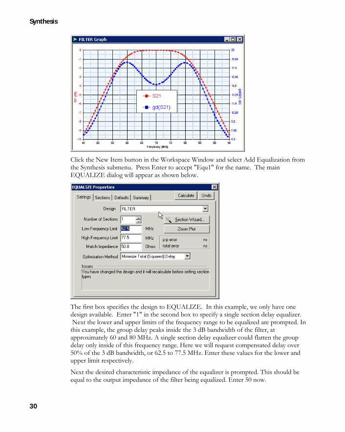
Synthesis
30
Click the New Item button in the Workspace Window and select Add Equalization from the Synthesis submenu. Press Enter to accept "Equ1" for the name. The main EQUALIZE dialog will appear as shown below.
The first box specifies the design to EQUALIZE. In this example, we only have one design available. Enter "1" in the second box to specify a single section delay equalizer. Next the lower and upper limits of the frequency range to be equalized are prompted. In this example, the group delay peaks inside the 3 dB bandwidth of the filter, at approximately 60 and 80 MHz. A single section delay equalizer could flatten the group delay only inside of this frequency range. Here we will request compensated delay over 50% of the 3 dB bandwidth, or 62.5 to 77.5 MHz. Enter these values for the lower and upper limit respectively.
Next the desired characteristic impedance of the equalizer is prompted. This should be equal to the output impedance of the filter being equalized. Enter 50 now.

EQUALIZE
31
The type of error function, least-square or peak-to-peak, should be selected. For now, select least-square. Least-square minimizes average delay error while peak-to-peak tends to minimize peak delay error.
Press "Apply" on the upper-right of the EQUALIZE dialog to begin the equalizer calculations. EQUALIZE estimates the required Fo and Q of the section to equalize the design. The program continues by optimizing the Fo and Q in an attempt to flatten the group delay of the cascaded data and delay equalizer. While EQUALIZE optimizes, the peak-to-peak delay, average delay, number of iterations, Fo, Q and 2 delay graphs (original and equalized) are displayed. When no additional improvement in the peak-to-peak delay occurs, the optimization will automatically stop.
Next, click on the section tab to choose the type of all-pass networks to be used. Select Type "2" for this section. (If this were a multiple section equalizer, types would be chosen for all sections. Characteristics of the various sections are discussed in the next section.) The final results should look like the figure below.
Section Types Nine different equalizer section types are available in EQUALIZE as shown below. (Section type 4 is actually three types, so eleven different types are available.) Types 1-6 use inductors, and capacitors, while Types 7-9 use operational amplifiers, capacitors, and resistors.
Note: Types 7-9 should only be used for filters designed for voltage gain (written with a high impedance output termination). They are generally used for filters created with A/FILTER

Synthesis
32

EQUALIZE
33
Section type 1 allows selection of the value of the bottom series capacitors which must be between inside a specified range. As they approach the minimum value, type 1 tends to type 3. As they approach the maximum value, type 1 tends to type 2. Types 2 and 3 are therefore minimum component versions of type 1.
Type 4 allows selection of the value of the bottom series inductors which must be inside a specified range. As they approaches the minimum value, the top series inductor vanishes
Synthesis
34
effectively creating a tenth type. As they approaches the maximum value, the shunt inductor vanishes creating an eleventh type.
Types 5 and 6 use coupled inductors, L2. These sections must be used if the Q of a section is less than 1, otherwise negative capacitor or inductor values result. Types 5 and 6 may also be used if Q>1. Equalizers for lowpass filters usually require one or more sections with a Q<1.
Type 5 is the most economic of components. However, type 5 requires a specific coupling coefficient, which is less convenient to realize than tight coupling near unity. Type 6 uses near unity coupling in the inductor at the expense of an additional inductor.
Type 7 is a multiple feedback allpass type that can be used for section Q between 0 and 20. Beyond 20, real-world op-amps cannot supply the required gain. This type can provide gain.
Type 8 is a dual amplifier allpass type and has a fixed gain. With the same op-amps, this type can be generally used at higher frequencies than a type 7 section. It can support a section Q between 0 and 150.
Type 9 is a biquad type that is more flexible than types 7 and 8 but requires one more op-amp than a type 8 section. It can provide gain, is easily tunable, and can be used for section Q between 0 and 200. In this type, R5 can be used for tuning.
Finite Q Components Finite-Q components increase the insertion loss of filters at the cutoff frequencies more than at low frequencies for lowpass filters and the center frequency of bandpass filters. This tends to “round” the response of bandpass filters. Finite-Q components used in group delay equalizers cause a transmission dip at the center frequency of each section.
To demonstrate this phenomenon, a two section equalizer with inductor Qs of 120 and capacitor Qs of 1000 was used to equalize a lossless 4th order Butterworth 44.5 to 50.5 MHz bandpass filter. A lossless bandpass filter was selected so the effects of equalizer component finite-Q could be readily observed. The results are given in the figure below. On a scale of 3 dB per division, the midband dip is just perceptible. The dip caused by each equalizer section blend into one midband dip and loss across the band of approximately 1 dB. The default finite Q values can be set from the Defaults tab in EQUALIZE.
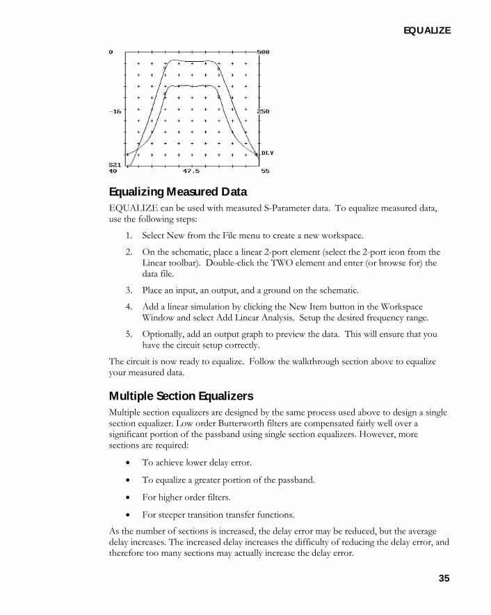
EQUALIZE
35
Equalizing Measured Data EQUALIZE can be used with measured S-Parameter data. To equalize measured data, use the following steps:
1. Select New from the File menu to create a new workspace.
2. On the schematic, place a linear 2-port element (select the 2-port icon from the Linear toolbar). Double-click the TWO element and enter (or browse for) the data file.
3. Place an input, an output, and a ground on the schematic.
4. Add a linear simulation by clicking the New Item button in the Workspace Window and select Add Linear Analysis. Setup the desired frequency range.
5. Optionally, add an output graph to preview the data. This will ensure that you have the circuit setup correctly.
The circuit is now ready to equalize. Follow the walkthrough section above to equalize your measured data.
Multiple Section Equalizers Multiple section equalizers are designed by the same process used above to design a single section equalizer. Low order Butterworth filters are compensated fairly well over a significant portion of the passband using single section equalizers. However, more sections are required:
• To achieve lower delay error.
• To equalize a greater portion of the passband.
• For higher order filters.
• For steeper transition transfer functions.
As the number of sections is increased, the delay error may be reduced, but the average delay increases. The increased delay increases the difficulty of reducing the delay error, and therefore too many sections may actually increase the delay error.

Synthesis
36
The peak-to-peak delay error is indicated during optimization in EQUALIZE. To determine the optimal number of sections for your circuit, click the Section Wizard button.
Group Delay Discontinuities As the number of sections becomes large, the rate of change of phase may become so large that the phase shift exceeds 180 degrees between frequency steps. This ambiguity will cause discontinuities in the group delay response produced by Linear Analysis. Should this occur, the following steps may be taken.
• Increase the number of frequency points.
• Decrease the frequency sweep range.
• Ignore the discontinuities. They do not exist in reality.
A second type of delay discontinuity exists in elliptic filters. The phase at a zero of transmission is discontinuous. An impulse may occur in the displayed delay. Because signal transmission at these frequencies is zero, or near zero, the delay impulse is a mathematical abstraction only. These delay impulses may also simply be ignored.
Exponent of the Error Function The user is given the option of selecting the type of error function, either least-square or Chebyshev. Least-square tends to minimize the average error. Chebyshev tends to an equiripple peak-to-peak delay error. This results in a minimum peak-to-peak error at the expense of the average peak-to-peak error across the specified equalization frequency range. This is illustrated in the figure below. On the left, Butterworth was selected and on the right Chebyshev was selected to equalize, with three sections, a 7th order Chebyshev .01 dB passband ripple lowpass filter. In each case, the delay was equalized past the cutoff to the peak of the unequalized delay at 4.6 MHz. The vertical axis of the delay response is offset from zero to increase the scale to 20 nS per division.
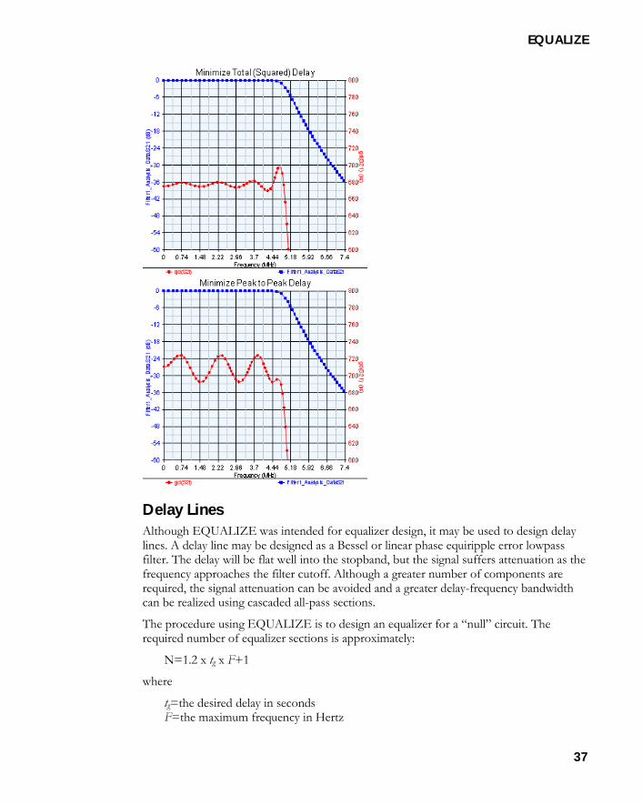
EQUALIZE
37
Delay Lines Although EQUALIZE was intended for equalizer design, it may be used to design delay lines. A delay line may be designed as a Bessel or linear phase equiripple error lowpass filter. The delay will be flat well into the stopband, but the signal suffers attenuation as the frequency approaches the filter cutoff. Although a greater number of components are required, the signal attenuation can be avoided and a greater delay-frequency bandwidth can be realized using cascaded all-pass sections.
The procedure using EQUALIZE is to design an equalizer for a “null” circuit. The required number of equalizer sections is approximately:
N=1.2 x tg x F+1
where
tg=the desired delay in seconds F=the maximum frequency in Hertz
Synthesis
38
The actual number is the next highest integer. This will result in a delay greater than desired. EQUALIZE is run with the integer number of sections and the desired upper frequency limit. The delay is then reduced to the desired value by rerunning EQUALIZE with an increased upper frequency scaled by the first pass and desired time delay ratio. This results in some margin in the upper frequency limit.
To create a delay line, use the following steps:
1. Select New from the File menu to create a new workspace.
2. On the schematic, place a resistor. Double-click the resistor and enter 0.01 for the impedance.
3. Place an input and an output on the schematic.
4. Add a linear simulation by right-clicking a folder or clicking the New Item button on the workspace tree toolbar. Setup the desired frequency range.
5. Optionally, add an output graph to preview the data. This will ensure that you have the circuit setup correctly.
The circuit is now ready to equalize. Follow the walkthrough section above to equalize the null circuit and create a delay line.
Consider the following example. A 1.1 microsecond delay line is required for up to 4.2 MHz in a 75 ohm system. The required N is 6.54, so 7 sections will be used. Follow the steps above, specifying 7 sections for EQUALIZE., peak-to-peak error approximation, a frequency range of 0 to 4.2 MHz and NULL.OUT as the output file. As the equalizer optimizes, the peak-to-peak delay error drops, and the average delay changes slowly. Once the peak-to-peak delay error is less than 1% of the average delay, further progress is slow. In this case, the average delay is approximately 1.218 microseconds when the peak-to-peak delay error drops below 12 nanoseconds.
Because the desired delay is 1.1 microseconds, EQUALIZE is rerun with an upper frequency limit of 1.218 / 1.1 times 4.2 MHz, which is 4.65 MHz. A delay of 1.1 microseconds is reached in approximately 80 iterations.
EQUALIZE: Concepts
Definitions The time required for a signal impressed on the input of a network to propagate to the output is generally a function of the signal frequency. This differential time delay may distort the signal waveform. Differential delay is a natural consequence of the filtering process. When the transition region of the filter response is steep, all minimum-phase filters exhibit differential delay.
When the phase shift versus frequency for a network is linear, the network exhibits delay which is constant with frequency. The signal is delayed in time, but no phase distortion occurs. The measure of delay often used is group delay, tg,and is defined as:
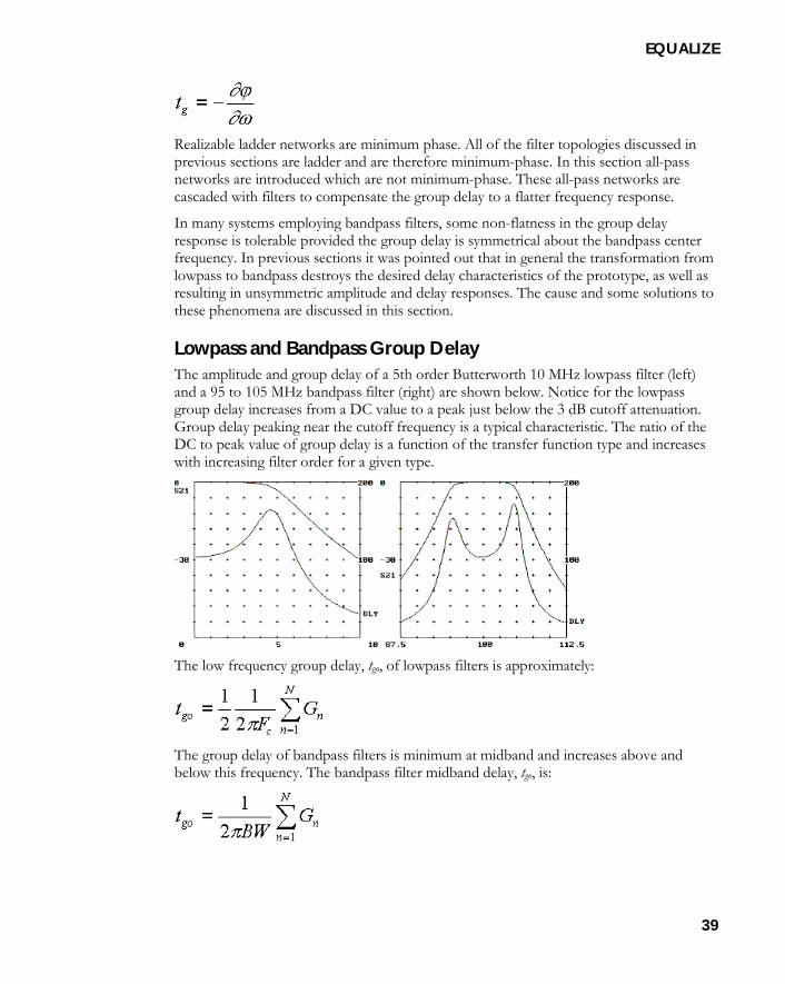
EQUALIZE
39
Realizable ladder networks are minimum phase. All of the filter topologies discussed in previous sections are ladder and are therefore minimum-phase. In this section all-pass networks are introduced which are not minimum-phase. These all-pass networks are cascaded with filters to compensate the group delay to a flatter frequency response.
In many systems employing bandpass filters, some non-flatness in the group delay response is tolerable provided the group delay is symmetrical about the bandpass center frequency. In previous sections it was pointed out that in general the transformation from lowpass to bandpass destroys the desired delay characteristics of the prototype, as well as resulting in unsymmetric amplitude and delay responses. The cause and some solutions to these phenomena are discussed in this section.
Lowpass and Bandpass Group Delay The amplitude and group delay of a 5th order Butterworth 10 MHz lowpass filter (left) and a 95 to 105 MHz bandpass filter (right) are shown below. Notice for the lowpass group delay increases from a DC value to a peak just below the 3 dB cutoff attenuation. Group delay peaking near the cutoff frequency is a typical characteristic. The ratio of the DC to peak value of group delay is a function of the transfer function type and increases with increasing filter order for a given type.
The low frequency group delay, tgo, of lowpass filters is approximately:
The group delay of bandpass filters is minimum at midband and increases above and below this frequency. The bandpass filter midband delay, tgo, is:

Synthesis
40
Highpass and Bandstop group delay Both lowpass and bandpass filters may readily be equalized using EQUALIZE. Highpass and bandstop filters may also be equalized to a degree. By definition the response of a highpass filter extends to infinite frequency. The equalization of highpass filter therefore involves sections with center frequencies from near the cutoff frequency to infinity, which requires an infinite number of sections.
In practice, the actual operating frequency range may be limited and not extend to infinite frequency. In this case, the specified equalization frequency range in EQUALIZE is set to the frequency range of interest. The delay in the passband above the specified frequency range will be less than within the equalized range. Feasibility depends on the required frequency range and the acceptable equalization error.
The situation is analogous for bandstop filters, where the upper passband is actually a highpass filter. Bandstop filter equalization actually consists of two equalizers individually designed, one for the lower passband and one for the upper passband. Two EQUALIZE instances are used, once to design the lowpass equalizer, and once more to design the highpass equalizer.
All-Pass Networks Nonmimimum-phase networks which exhibit a flat amplitude frequency response but which have a prescribed phase response are called all-pass networks or delay equalizers. This type of network may be cascaded with a filter to flatten the group delay frequency response. Delay equalizers are realized as lattice or bridge networks.
A delay equalizer used to compensate the group delay of a filter consists of one or more fundamental sections cascaded together. The group delay of each section is approximately parabolic, with a peak at a specified center frequency. Each section is an all-pass transfer function of first, second or higher order. Second order sections exhibit the necessary characteristics to compensate filter group delay, are economic and are more realizable in general than first order all-pass networks.
The constant resistance lattice is the starting point for all-pass network design. From this network, a variety of 2nd order bridge-tee all-pass networks may be derived. Schematics for the nine types used in EQUALIZE are shown below. Component values are derived from the center frequency, Fo, and Q required for each section. Manual determination of the required Fo and Q for each all-pass section to optimally compensate the group delay of a filter is an approximate and tedious process, particularly for higher order filers or if precise compensation is required. EQUALIZE automates all aspects of the design process.
Delay Symmetry It has been mentioned that the transformation from lowpass to bandpass results in the destruction of the delay properties of the lowpass prototype and bandpass filters with poor arithmetic amplitude and group delay symmetry, particularly for larger bandwidths.
EQUALIZE
41
The full bandpass transform, in which each shunt capacitor in the lowpass prototype is converted to a shunt parallel L-C network and each series inductor is converted to a series L-C, results in geometric amplitude symmetry. However, when symmetry is required, it is more often arithmetic symmetry which is required. Moreover, the full transform does not result in group delay symmetry. Actually, no commonly used transform results in arithmetic or delay symmetry for wide bandwidths.
In a relatively unknown paper, Carassa offers a proof that topologies of filters with three zeros of transmission at infinite frequency for each zero at DC can exhibit arithmetic amplitude and delay symmetry. We will refer to the ratio of zeros at infinite frerquency to zeros at DC as the multiplicity ratio. Of all the bandpass transforms previously discussed, only a second order shunt-C coupled bandpass filter without end coupling capacitors and the special Blinchikoff wide-band constant delay bandpass filter have a multiplicity ratio of three.
To determine the multiplicity ratio of a filter, at infinite frequency each inductor is replaced with an imaginary open circuit and each capacitor with an imaginary short circuit. Series connected open circuits are equivalent to one open circuit. Parallel short circuits to ground are equivalent to one short circuit. The resulting number of equivalent open and shorts is the number of zeros at infinite frequency. A similar process is repeated at DC, where each capacitor is an open circuit and each inductor is a short circuit. As an exercise, you may prove to yourself that the multiplicity ratio of the Blinchikoff filter is three.
Repairing poor symmetry Although few bandpass filter topologies have a multiplicity ratio of three, the topology may often be modified to achieve a multiplicity near three. After component values are adjusted to correct the effects of the topology shift, the filter will exhibit better symmetry. Optimization may be employed to adjust component values after a topology shift.
The multiplicity of the full transform bandpass filters is one. Because the number of zeros at infinity is too low, the selectivity is greater below the passband, the delay peak is greater at the low end of the passband.
The multiplicity ratio of the top-C coupled bandpass filter is a function of the order, but is never greater than 0.33, so this filter is highly unsymmetrical for wide bandwidths.
The multiplicity ratio of the shunt-C coupled bandpass filter ranges from three for 2nd order with no end coupling capacitors to increasing values with increasing order. By converting an appropriate number of shunt coupling capacitors to coupling inductors, a multiplicity ratio of approximately three can be achieved for arbitrary order. Conversion of a shunt coupling capacitor to a shunt coupling inductor is illustrated in the FILTER section of the Classic Filter Synthesis manual.
Symmetry can be acheived in elliptic function filters as well by applying Carassa’s rule. The zig-zag minimum inductance bandpass filter has a multiplicity ratio of one for all orders. By converting the input shunt inductor to a series inductance, a multiplicity of three is achieved for all orders. An example of this process is given in the FILTER section of the Classic Filter Synthesis manual.

Synthesis
42
Another powerful tool for dealing with this problem is Eagleware’s symmetric transform described in the Classic Filter Synthesis manual.
43
Chapter 4: FILTER
FILTER: Operation
Overview
Note: Additional documentation for FILTER is given online in the HF Filter Design and Computer Simulation book.
FILTER makes designing L-C filters and delay equalizers a snap. With GENESYS you can simulate the filter performance, customize or optimize the filter and check the effects of parasitics.
FILTER synthesizes many L-C filter types suitable for a wide range of applications. Principle features include:
• 20 filter topologies
• Topology choices provide for practical realizations and specific application needs
• A wide range of transfer approximations (amplitude and delay response shapes)
• Effective noise bandwidth calculation
• Complete integration with GENESYS
Walkthrough In this walkthrough, the following filter is designed:
• 50 Ω source and load terminations
• Chebyshev lowpass filter
• 0.25 dB of passband ripple
• 7th order
• 70 MHz cutoff frequency
• Minimum capacitor configuration
Create a new filter by clicking the "New Item" button on the Workspace Tree toolbar, and choose "Add Passive Filter" as shown below.
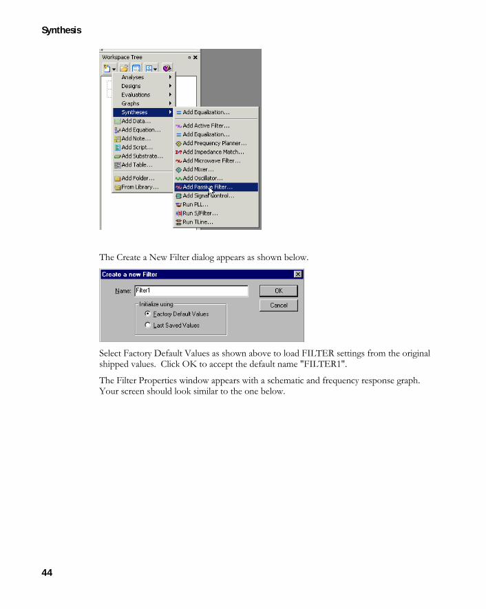
Synthesis
44
The Create a New Filter dialog appears as shown below.
Select Factory Default Values as shown above to load FILTER settings from the original shipped values. Click OK to accept the default name "FILTER1".
The Filter Properties window appears with a schematic and frequency response graph. Your screen should look similar to the one below.
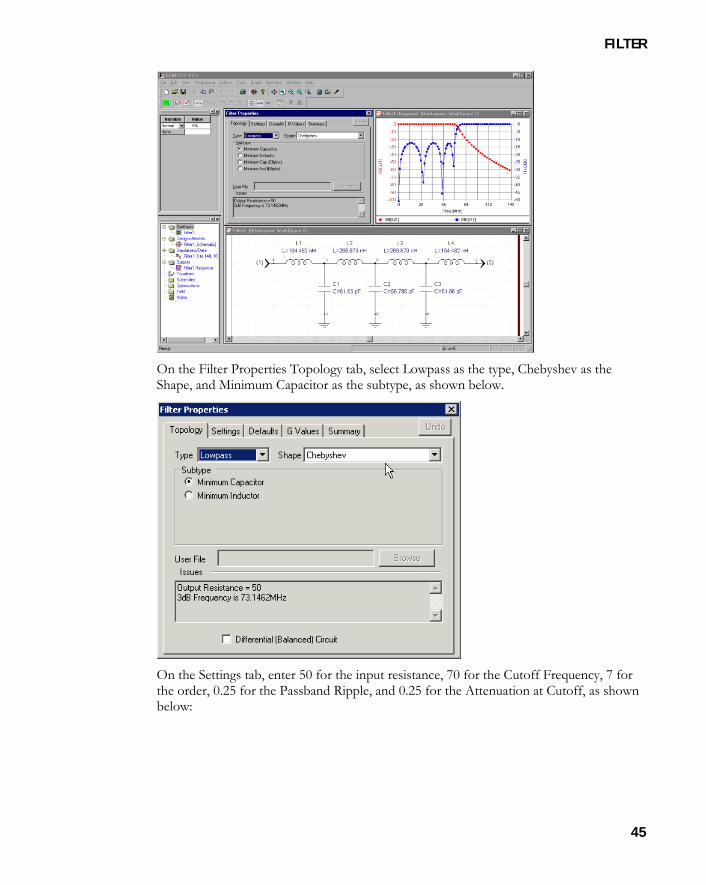
FILTER
45
On the Filter Properties Topology tab, select Lowpass as the type, Chebyshev as the Shape, and Minimum Capacitor as the subtype, as shown below.
On the Settings tab, enter 50 for the input resistance, 70 for the Cutoff Frequency, 7 for the order, 0.25 for the Passband Ripple, and 0.25 for the Attenuation at Cutoff, as shown below:
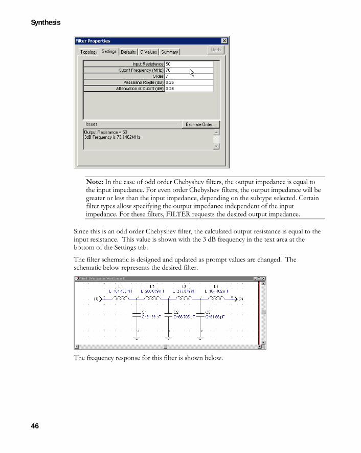
Synthesis
46
Note: In the case of odd order Chebyshev filters, the output impedance is equal to the input impedance. For even order Chebyshev filters, the output impedance will be greater or less than the input impedance, depending on the subtype selected. Certain filter types allow specifying the output impedance independent of the input impedance. For these filters, FILTER requests the desired output impedance.
Since this is an odd order Chebyshev filter, the calculated output resistance is equal to the input resistance. This value is shown with the 3 dB frequency in the text area at the bottom of the Settings tab.
The filter schematic is designed and updated as prompt values are changed. The schematic below represents the desired filter.
The frequency response for this filter is shown below.
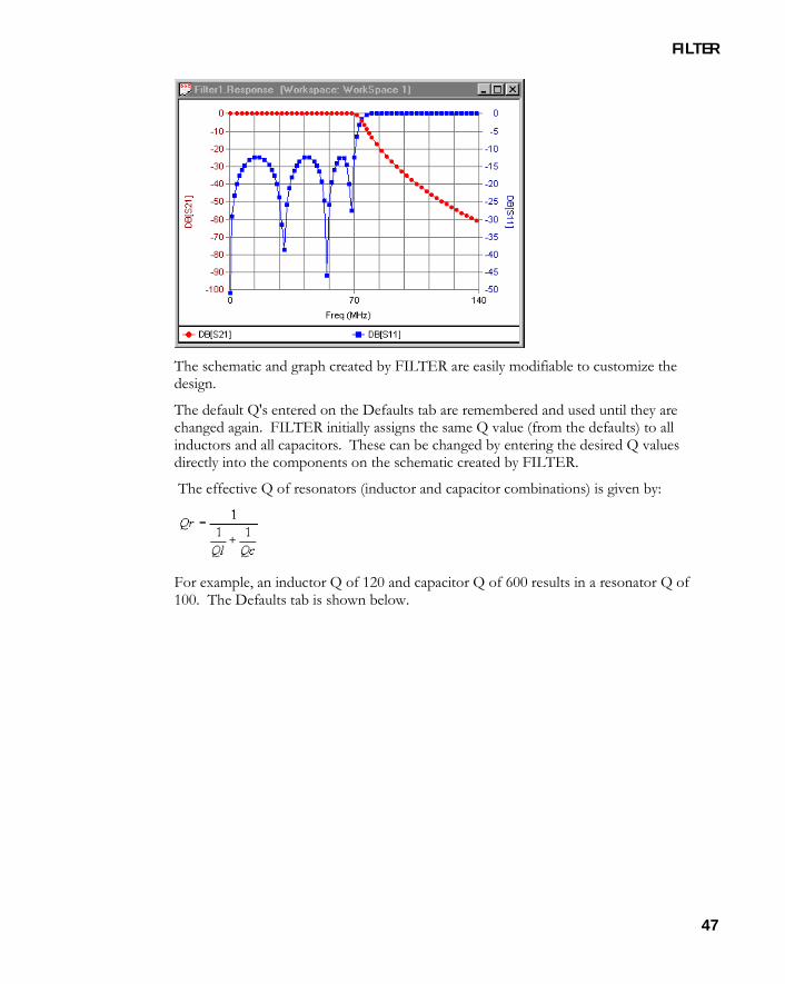
FILTER
47
The schematic and graph created by FILTER are easily modifiable to customize the design.
The default Q's entered on the Defaults tab are remembered and used until they are changed again. FILTER initially assigns the same Q value (from the defaults) to all inductors and all capacitors. These can be changed by entering the desired Q values directly into the components on the schematic created by FILTER.
The effective Q of resonators (inductor and capacitor combinations) is given by:
For example, an inductor Q of 120 and capacitor Q of 600 results in a resonator Q of 100. The Defaults tab is shown below.
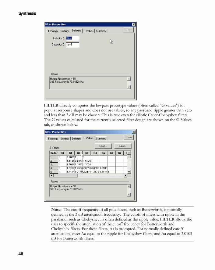
Synthesis
48
FILTER directly computes the lowpass prototype values (often called "G values") for popular response shapes and does not use tables, so any passband ripple greater than zero and less than 3 dB may be chosen. This is true even for elliptic Cauer-Chebyshev filters. The G values calculated for the currently selected filter design are shown on the G Values tab, as shown below.
Note: The cutoff frequency of all-pole filters, such as Butterworth, is normally defined as the 3 dB attenuation frequency. The cutoff of filters with ripple in the passband, such as Chebyshev, is often defined as the ripple value. FILTER allows the user to specify the attenuation of the cutoff frequency for Butterworth and Chebyshev filters. For these filters, Aa is prompted. For normally defined cutoff attenuation, enter Aa equal to the ripple for Chebyshev filters, and Aa equal to 3.0103 dB for Butterworth filters.
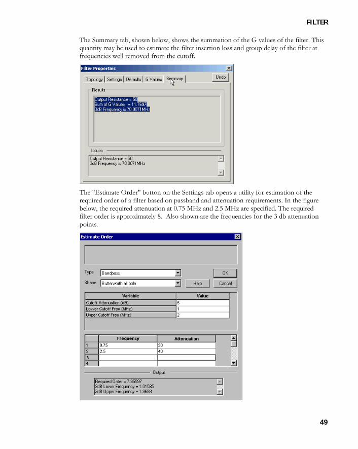
FILTER
49
The Summary tab, shown below, shows the summation of the G values of the filter. This quantity may be used to estimate the filter insertion loss and group delay of the filter at frequencies well removed from the cutoff.
The "Estimate Order" button on the Settings tab opens a utility for estimation of the required order of a filter based on passband and attenuation requirements. In the figure below, the required attenuation at 0.75 MHz and 2.5 MHz are specified. The required filter order is approximately 8. Also shown are the frequencies for the 3 db attenuation points.
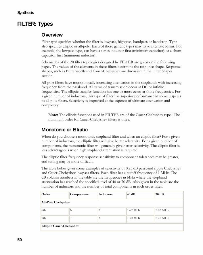
Synthesis
50
FILTER: Types
Overview Filter type specifies whether the filter is lowpass, highpass, bandpass or bandstop. Type also specifies elliptic or all-pole. Each of these generic types may have alternate forms. For example, the lowpass type, can have a series inductor first (minimum capacitor) or a shunt capacitor first (minimum inductor).
Schematics of the 20 filter topologies designed by FILTER are given on the following pages. The values of the elements in these filters determine the response shape. Response shapes, such as Butterworth and Cauer-Chebyshev are discussed in the Filter Shapes section.
All-pole filters have monotonically increasing attenuation in the stopbands with increasing frequency from the passband. All zeros of transmission occur at DC or infinite frequencies. The elliptic transfer function has one or more zeros at finite frequencies. For a given number of inductors, this type of filter has superior performance in some respects to all-pole filters. Selectivity is improved at the expense of ultimate attenuation and complexity.
Note: The elliptic functions used in FILTER are of the Cauer-Chebyshev type. The minimum order for Cauer-Chebyshev filters is three.
Monotonic or Elliptic When do you choose a monotonic stopband filter and when an elliptic filter? For a given number of inductors, the elliptic filter will give better selectivity. For a given number of components, the monotonic filter will generally give better selectivity. The elliptic filter is less advantageous when high stopband attenuation is required.
The elliptic filter frequency response sensitivity to component tolerances may be greater, and tuning may be more difficult.
The table below gives some examples of selectivity of 0.25 dB passband ripple Chebyshev and Cauer-Chebyshev lowpass filters. Each filter has a cutoff frequency of 1 MHz. The dB column numbers in the table are the frequencies in MHz where the stopband attenuation has reached the specified level of 40 or 70 dB. Also given in the table are the number of inductors and the number of total components in each order filter.
Order Components Inductors 40 dB 70 dB
All-Pole Chebyshev
6th 6 3 1.69 MHz 2.82 MHz
7th 7 3 1.50 MHz 2.25 MHz
Elliptic Cauer-Chebyshev

FILTER
51
4th 5 2 1.76 MHz 3.88 MHz
5th 7 2 1.34 MHz 2.32 MHz
6th 8 3 1.16 MHz 1.70 MHz
7th 10 3 1.08 MHz 1.40 MHz
Minimum Inductor All-Pole Lowpass Minimum Capacitor All-Pole Lowpass
Minimum inductor (top) and minimum capacitor (bottom) subtypes are the lowpass options. Because inductors are usually larger, more expensive and have lower Q, minimum inductance filters are normally the first choice. For even order, both types have an equal number of inductors and capacitors, so subtype choice is less significant.
Both types are open to ground and pass DC. However, at frequencies well into cutoff, a series inductor becomes a high impedance and a shunt capacitor becomes a low impedance. This may affect the selection in some applications, such as diplexers or in active interstage coupling networks where stability may be a factor.
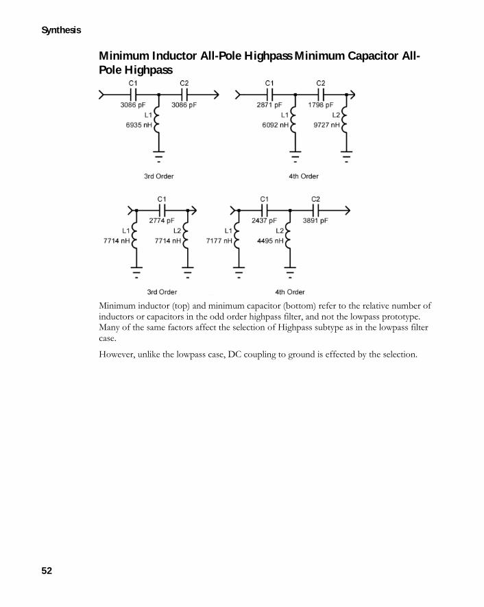
Synthesis
52
Minimum Inductor All-Pole Highpass Minimum Capacitor All-Pole Highpass
Minimum inductor (top) and minimum capacitor (bottom) refer to the relative number of inductors or capacitors in the odd order highpass filter, and not the lowpass prototype. Many of the same factors affect the selection of Highpass subtype as in the lowpass filter case.
However, unlike the lowpass case, DC coupling to ground is effected by the selection.
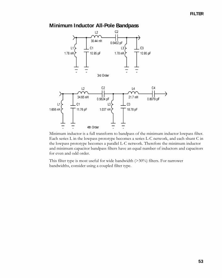
FILTER
53
Minimum Inductor All-Pole Bandpass
Minimum inductor is a full transform to bandpass of the minimum inductor lowpass filter. Each series L in the lowpass prototype becomes a series L-C network, and each shunt C in the lowpass prototype becomes a parallel L-C network. Therefore the minimum inductor and minimum capacitor bandpass filters have an equal number of inductors and capacitors for even and odd order.
This filter type is most useful for wide bandwidth (>30%) filters. For narrower bandwidths, consider using a coupled filter type.
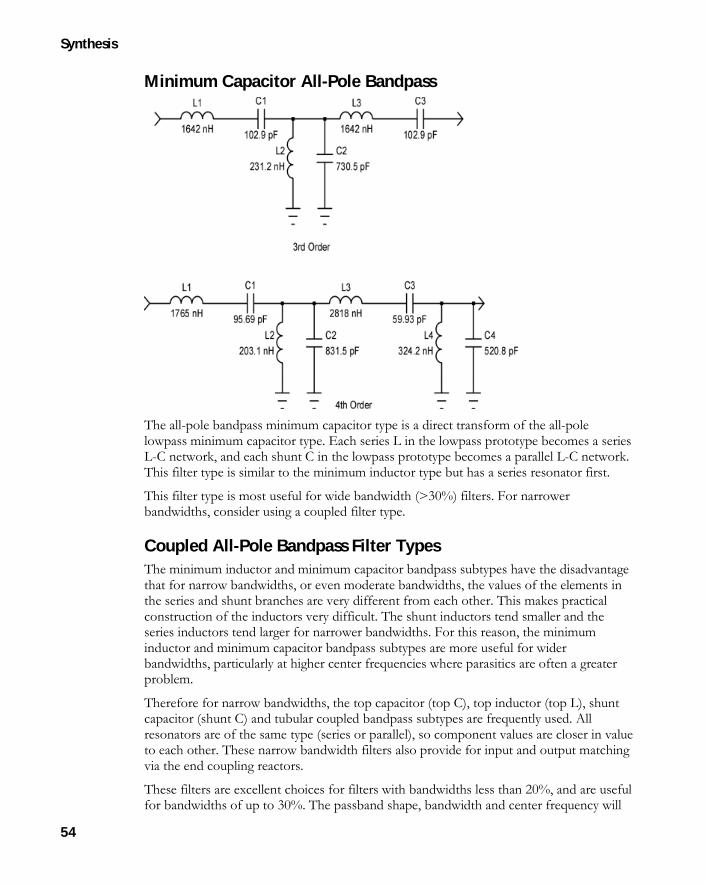
Synthesis
54
Minimum Capacitor All-Pole Bandpass
The all-pole bandpass minimum capacitor type is a direct transform of the all-pole lowpass minimum capacitor type. Each series L in the lowpass prototype becomes a series L-C network, and each shunt C in the lowpass prototype becomes a parallel L-C network. This filter type is similar to the minimum inductor type but has a series resonator first.
This filter type is most useful for wide bandwidth (>30%) filters. For narrower bandwidths, consider using a coupled filter type.
Coupled All-Pole Bandpass Filter Types The minimum inductor and minimum capacitor bandpass subtypes have the disadvantage that for narrow bandwidths, or even moderate bandwidths, the values of the elements in the series and shunt branches are very different from each other. This makes practical construction of the inductors very difficult. The shunt inductors tend smaller and the series inductors tend larger for narrower bandwidths. For this reason, the minimum inductor and minimum capacitor bandpass subtypes are more useful for wider bandwidths, particularly at higher center frequencies where parasitics are often a greater problem.
Therefore for narrow bandwidths, the top capacitor (top C), top inductor (top L), shunt capacitor (shunt C) and tubular coupled bandpass subtypes are frequently used. All resonators are of the same type (series or parallel), so component values are closer in value to each other. These narrow bandwidth filters also provide for input and output matching via the end coupling reactors.
These filters are excellent choices for filters with bandwidths less than 20%, and are useful for bandwidths of up to 30%. The passband shape, bandwidth and center frequency will
FILTER
55
increase in error for larger bandwidths. The routines in =FILTER= apply the Cohn lowpass to bandpass accuracy enhancements for these topologies [2].
Also, for wider bandwidths, the stopband and skirts of these topologies become asymmetric. For the top-C bandpass filter, the stopband and skirt above the passband suffer. For the shunt-C, top-L and tubular topologies the stopband and skirt below the passband suffer. As the bandwidth is narrowed, the symmetry of these filters improves, and as the bandwidth is widened, the symmetry of the response worsens.
For wider bandwidths, the order requirement determined by the N-Help routine in =FILTER= is pessimistic on one side or the other for these subtypes. Often, selectivity is more important on one side than another, and the subtype choice can be made accordingly. Otherwise, a higher order, a narrower bandwidth or the full transform filters must be used. Sample responses are shown on the following pages to illustrate this issue.
Mixed Coupling Reactors If selectivity is almost adequate, the trick of changing a coupling capacitor to an inductor can improve selectivity on one side at the expensive of the selectivity on the other side. An example of this transform is given in Chapter 3. This technique may also be used to change the DC coupling or stopband impedance characteristics of these filters.
Eagleware sometimes receives requests to include approximate transform bandpass filters with mixed coupling elements, such as alternating capacitors and inductors. These filter types were not included for a specific reason. Approximate transform bandpass filters designed without the Cohn correction mentioned earlier are limited to an upper bandwidth limit of 2-5% percent, otherwise the resulting response has a significant frequency shift. Bandpass filters designed with practical inductor Q’s are limited to bandwidths greater than 2-5% percent. Therefore, in general, there is no acceptable bandwidth for accurate design of this type of practical bandpass filters without the Cohn correction. Unfortunately the Cohn correction only applies to like coupling elements.
The problem is not that a solution does not exist. The problem is that the closed formulas are not known. These filters can be designed by converting a coupling element type and using tuning or optimization techniques.

Synthesis
56
Top C Coupled All-Pole Bandpass
5th order filter schematic and typical response.
The top-C bandpass filter subtype consists of shunt parallel resonant L-C circuits coupled via series capacitors. This type of filter is an approximate transform, with decreasing accuracy for increasing bandwidths. It is most accurate (and useful) for bandwidths of less than 30%.
This type is very practical since all inductors are the same value, and that value can be specified by the user. Optionally, by choosing an inductor value just inside the given limit, the input and output coupling capacitors will become large enough so that they may be eliminated from the design.
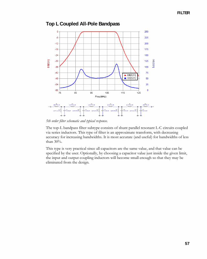
FILTER
57
Top L Coupled All-Pole Bandpass
5th order filter schematic and typical response.
The top-L bandpass filter subtype consists of shunt parallel resonant L-C circuits coupled via series inductors. This type of filter is an approximate transform, with decreasing accuracy for increasing bandwidths. It is most accurate (and useful) for bandwidths of less than 30%.
This type is very practical since all capacitors are the same value, and that value can be specified by the user. Optionally, by choosing a capacitor value just inside the given limit, the input and output coupling inductors will become small enough so that they may be eliminated from the design.
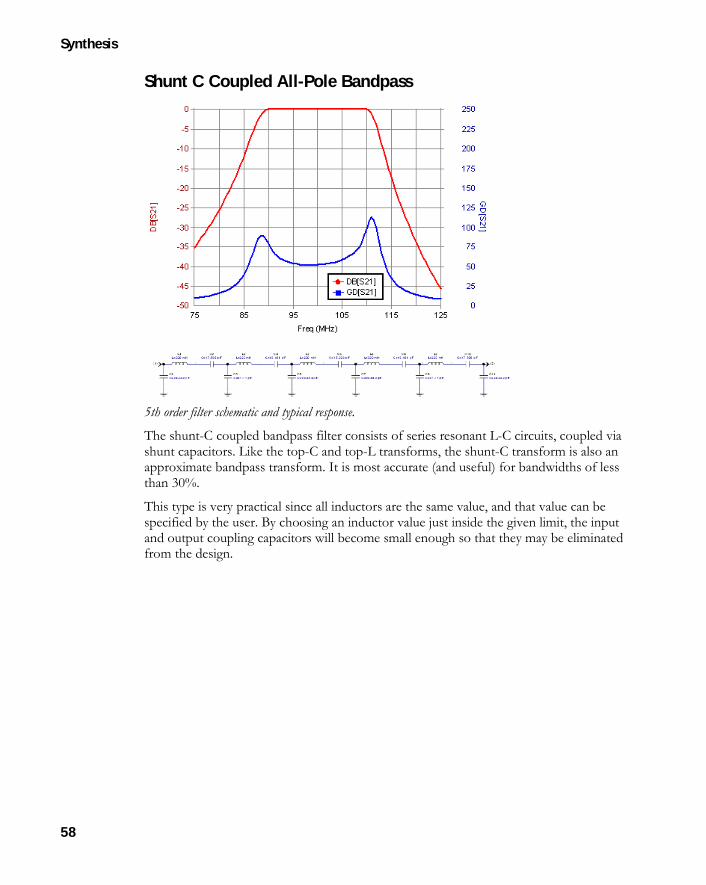
Synthesis
58
Shunt C Coupled All-Pole Bandpass
5th order filter schematic and typical response.
The shunt-C coupled bandpass filter consists of series resonant L-C circuits, coupled via shunt capacitors. Like the top-C and top-L transforms, the shunt-C transform is also an approximate bandpass transform. It is most accurate (and useful) for bandwidths of less than 30%.
This type is very practical since all inductors are the same value, and that value can be specified by the user. By choosing an inductor value just inside the given limit, the input and output coupling capacitors will become small enough so that they may be eliminated from the design.
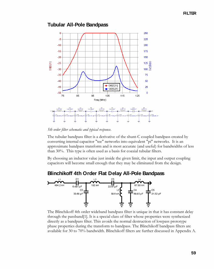
FILTER
59
Tubular All-Pole Bandpass
5th order filter schematic and typical response.
The tubular bandpass filter is a derivative of the shunt-C coupled bandpass created by converting internal capacitor "tee" networks into equivalent "pi" networks. It is an approximate bandpass transform and is most accurate (and useful) for bandwidths of less than 30%. This type is often used as a basis for coaxial tubular filters.
By choosing an inductor value just inside the given limit, the input and output coupling capacitors will become small enough that they may be eliminated from the design.
Blinchikoff 4th Order Flat Delay All-Pole Bandpass
The Blinchikoff 4th order wideband bandpass filter is unique in that it has constant delay through the passband[1]. It is a special class of filter whose properties were synthesized directly as a bandpass filter. This avoids the normal destruction of lowpass prototype phase properties during the transform to bandpass. The Blinchikoff bandpass filters are available for 30 to 70% bandwidth. Blinchikoff filters are further discussed in Appendix A.
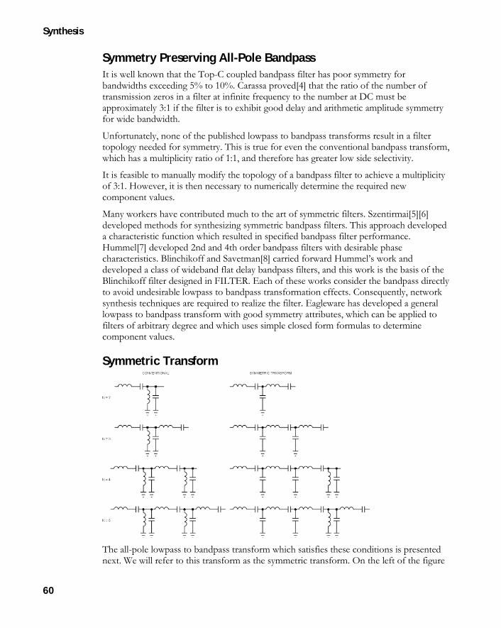
Synthesis
60
Symmetry Preserving All-Pole Bandpass It is well known that the Top-C coupled bandpass filter has poor symmetry for bandwidths exceeding 5% to 10%. Carassa proved[4] that the ratio of the number of transmission zeros in a filter at infinite frequency to the number at DC must be approximately 3:1 if the filter is to exhibit good delay and arithmetic amplitude symmetry for wide bandwidth.
Unfortunately, none of the published lowpass to bandpass transforms result in a filter topology needed for symmetry. This is true for even the conventional bandpass transform, which has a multiplicity ratio of 1:1, and therefore has greater low side selectivity.
It is feasible to manually modify the topology of a bandpass filter to achieve a multiplicity of 3:1. However, it is then necessary to numerically determine the required new component values.
Many workers have contributed much to the art of symmetric filters. Szentirmai[5][6] developed methods for synthesizing symmetric bandpass filters. This approach developed a characteristic function which resulted in specified bandpass filter performance. Hummel[7] developed 2nd and 4th order bandpass filters with desirable phase characteristics. Blinchikoff and Savetman[8] carried forward Hummel’s work and developed a class of wideband flat delay bandpass filters, and this work is the basis of the Blinchikoff filter designed in FILTER. Each of these works consider the bandpass directly to avoid undesirable lowpass to bandpass transformation effects. Consequently, network synthesis techniques are required to realize the filter. Eagleware has developed a general lowpass to bandpass transform with good symmetry attributes, which can be applied to filters of arbitrary degree and which uses simple closed form formulas to determine component values.
Symmetric Transform
The all-pole lowpass to bandpass transform which satisfies these conditions is presented next. We will refer to this transform as the symmetric transform. On the left of the figure

FILTER
61
above are the topologies of conventional bandpass filters for orders two through five. We use the convention that bandpass filter order is equal to the order of the lowpass prototype from which it is developed. While not rigorous, the convention is broadly used.
Shown above are the topologies of the symmetric bandpass filters of corresponding order. The symmetric bandpass filter topology results when the first and then every other shunt parallel resonator is replaced with a series resonator. The parallel to series resonator conversion is based on impedance inverters as published by Cohn[9]. It can be shown that the multiplicity ratio of these symmetric transform filters for even order is 3:1 and asymptotically approaches 3:1 with increasing odd order. The remaining task is therefore to find a process for determining component values. An approximate solution is known and is the technique utilized in the symmetric transform incorporated in the FILTER program.
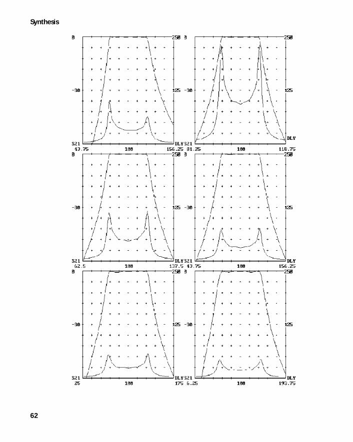
Synthesis
62
FILTER
63
Shown on the above figure are the amplitude and delay responses for a conventional 6th order 0.1 dB ripple Chebyshev bandpass filter with 45% arithmetic bandwidth centered at 100 MHz, and for 6th order 0.1 dB ripple Chebyshev symmetric transform bandpass filters designed by FILTER for 15%, 30%, 45%, 60% and 75% bandwidths. (The 75% filter was tuned in Genesys). The results illustrate marvelous symmetry.
SYMMETRIC TRANSFORM LIMITATIONS The approximate method used to compute component values limits the practical bandwidth. Depending on the acceptable levels of center frequency error, ripple or response error, and return loss, bandwidths to 40% or 50% are generally practical. If some error in the response is acceptable, for certain lowpass prototypes, or if optimization is employed, greater bandwidths may be specified.
For wider bandwidth the passband is not equi-ripple, but the response is improved by tuning the resonator inductors or capacitors. The 75% bandwidth filter shown above required tuning of the resonators using Genesys.
For even wider bandwidths, some element values may be negative. The bandwidth at which this occurs is a function of the lowpass prototype selected. Prototypes with a large variation in G values, such as is the case with controlled phase prototypes, may be restricted to 20% or less bandwidth. It may be possible to extend the bandwidth before negative values result by reversing the order of the G-values. The delay preserving attributes of the symmetric transform is not as desirable as the symmetry attributes.
The practical lower BW limit is similar to the conventional bandpass filter. As the bandwidth decreases, the ratio of the inductors in the series and shunt branches becomes extreme. For bandwidths below approximately 5% to 10%, the symmetry of the top-C coupled and the shunt-C coupled bandpass filters is generally acceptable, and these filters are preferred.
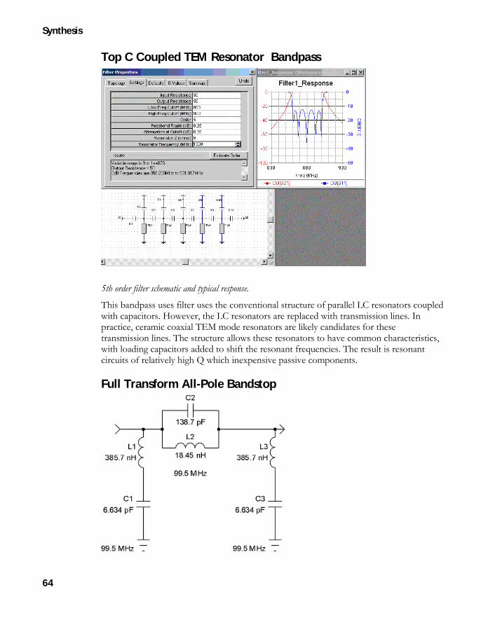
Synthesis
64
Top C Coupled TEM Resonator Bandpass
5th order filter schematic and typical response.
This bandpass uses filter uses the conventional structure of parallel LC resonators coupled with capacitors. However, the LC resonators are replaced with transmission lines. In practice, ceramic coaxial TEM mode resonators are likely candidates for these transmission lines. The structure allows these resonators to have common characteristics, with loading capacitors added to shift the resonant frequencies. The result is resonant circuits of relatively high Q which inexpensive passive components.
Full Transform All-Pole Bandstop
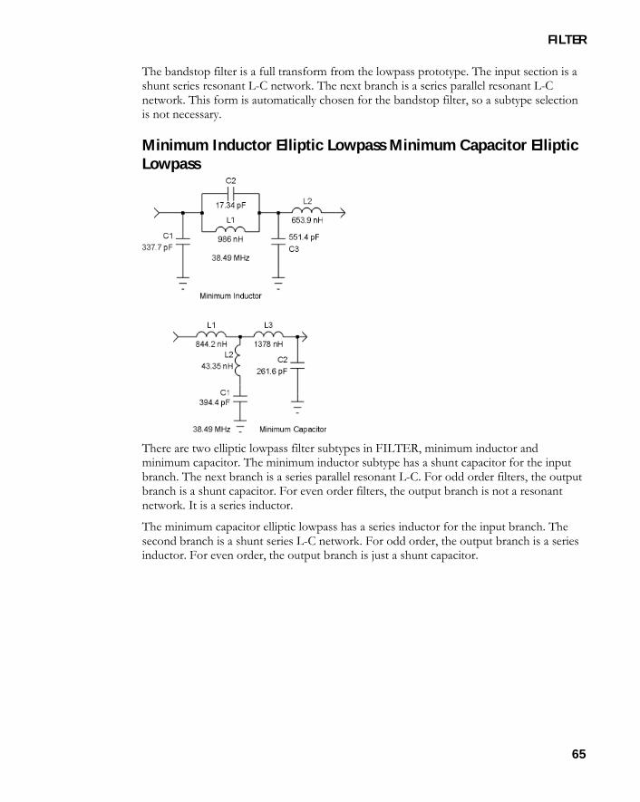
FILTER
65
The bandstop filter is a full transform from the lowpass prototype. The input section is a shunt series resonant L-C network. The next branch is a series parallel resonant L-C network. This form is automatically chosen for the bandstop filter, so a subtype selection is not necessary.
Minimum Inductor Elliptic Lowpass Minimum Capacitor Elliptic Lowpass
There are two elliptic lowpass filter subtypes in FILTER, minimum inductor and minimum capacitor. The minimum inductor subtype has a shunt capacitor for the input branch. The next branch is a series parallel resonant L-C. For odd order filters, the output branch is a shunt capacitor. For even order filters, the output branch is not a resonant network. It is a series inductor.
The minimum capacitor elliptic lowpass has a series inductor for the input branch. The second branch is a shunt series L-C network. For odd order, the output branch is a series inductor. For even order, the output branch is just a shunt capacitor.
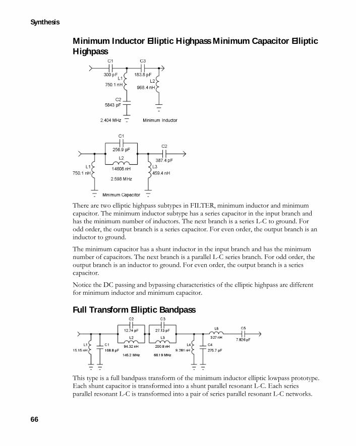
Synthesis
66
Minimum Inductor Elliptic Highpass Minimum Capacitor Elliptic Highpass
There are two elliptic highpass subtypes in FILTER, minimum inductor and minimum capacitor. The minimum inductor subtype has a series capacitor in the input branch and has the minimum number of inductors. The next branch is a series L-C to ground. For odd order, the output branch is a series capacitor. For even order, the output branch is an inductor to ground.
The minimum capacitor has a shunt inductor in the input branch and has the minimum number of capacitors. The next branch is a parallel L-C series branch. For odd order, the output branch is an inductor to ground. For even order, the output branch is a series capacitor.
Notice the DC passing and bypassing characteristics of the elliptic highpass are different for minimum inductor and minimum capacitor.
Full Transform Elliptic Bandpass
This type is a full bandpass transform of the minimum inductor elliptic lowpass prototype. Each shunt capacitor is transformed into a shunt parallel resonant L-C. Each series parallel resonant L-C is transformed into a pair of series parallel resonant L-C networks.
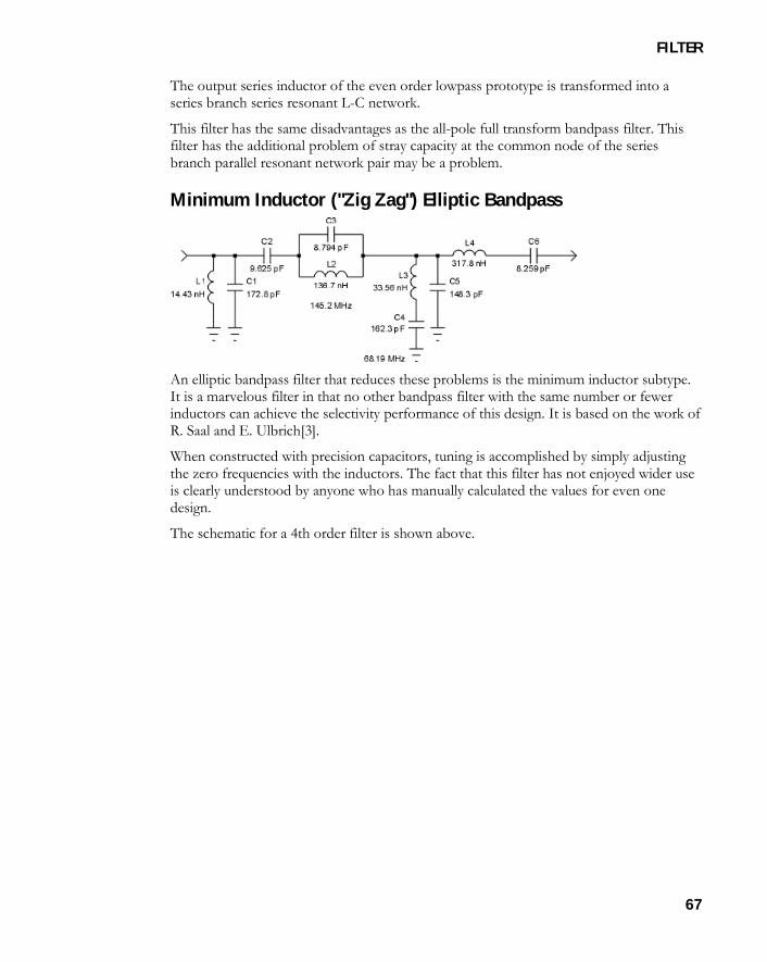
FILTER
67
The output series inductor of the even order lowpass prototype is transformed into a series branch series resonant L-C network.
This filter has the same disadvantages as the all-pole full transform bandpass filter. This filter has the additional problem of stray capacity at the common node of the series branch parallel resonant network pair may be a problem.
Minimum Inductor ("Zig Zag") Elliptic Bandpass
An elliptic bandpass filter that reduces these problems is the minimum inductor subtype. It is a marvelous filter in that no other bandpass filter with the same number or fewer inductors can achieve the selectivity performance of this design. It is based on the work of R. Saal and E. Ulbrich[3].
When constructed with precision capacitors, tuning is accomplished by simply adjusting the zero frequencies with the inductors. The fact that this filter has not enjoyed wider use is clearly understood by anyone who has manually calculated the values for even one design.
The schematic for a 4th order filter is shown above.

Synthesis
68
Elliptic Parametric Bandpass Filter
5th order filter schematic and typical response.
Elliptic filters offer improved rejection near the passband than all-pole filters. However, the topology of conventional elliptic bandpass does not lend themselves to construction using simple resonators but rather require 3-element dipoles.
This elliptic bandpass filter can be built using conventional parallel resonators. When implemented as coaxial resonators, improved unloaded Q and lower filter insertion loss can be achieved. Anti-resonant circuits are required to couple the parallel resonators, but the unloaded Q of these coupling elements is not as critical as the Q of the resonators.
This structure can also be designed by applying Norton transforms to the conventional elliptic bandpass. The GENESYS module S/FILTER can be used to design similar structures but with user control of the placement of all transmission zeros. For high performance, high volume filter designs, S/FILTER is suggested. For quick design of elliptic filters with conventional zero placement, this topology may be used.
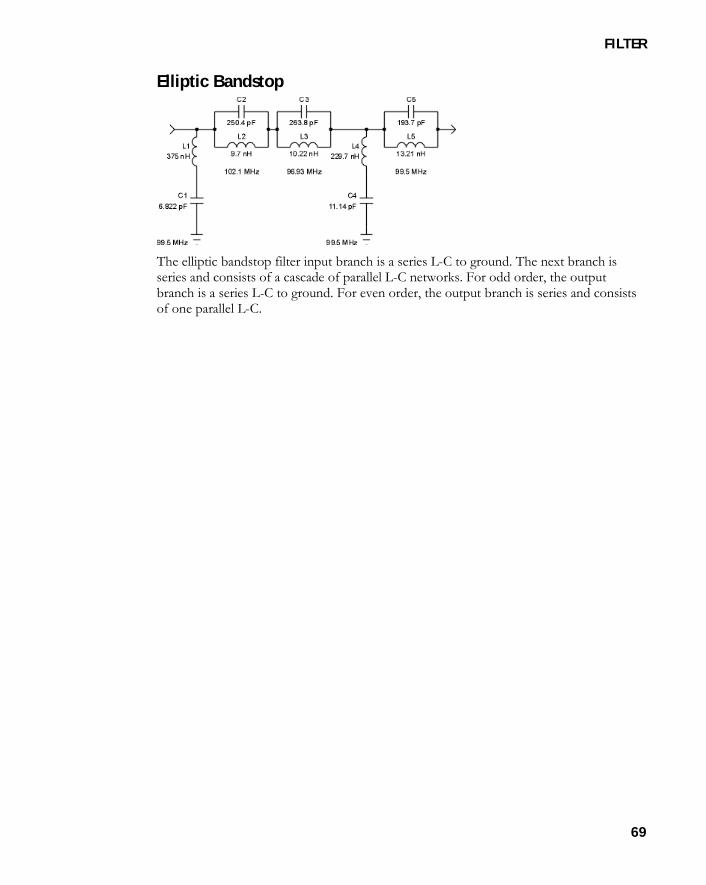
FILTER
69
Elliptic Bandstop
The elliptic bandstop filter input branch is a series L-C to ground. The next branch is series and consists of a cascade of parallel L-C networks. For odd order, the output branch is a series L-C to ground. For even order, the output branch is series and consists of one parallel L-C.

71
Chapter 5: MATCH
MATCH: Operation
Overview MATCH offers a variety of matching network solutions from simple networks to those suitable for demanding applications such as broad bandwidth, high source and load impedance ratios, frequency dependent terminations, multiple stages, and non-unilateral active devices.
MATCH is used to automatically synthesize lumped and distributed matching networks. These networks can be complex and broadband. Unlike simpler Smith Chart based matching programs, your circuit complexity is not limited by what can be easily visualized on a Smith Chart. MATCH can also design matching networks for multi-stage amplifiers.
MATCH synthesizes a variety of distributed (TRL) and lumped (L-C) matching networks for use in the cascade. These types are:
• L-C Pi Network
• L-C Tee Network
• TRL 1/4 Wave
• TRL Single/Double Stub
• L-C Bandpass
• L-C Pseudo Lowpass
• TRL Pseudo Lowpass
• TRL Stepped Impedance
• Custom
Each network type in MATCH uses its own algorithm to compute starting values and has its own unique characteristics. A good understanding of the different network types will help to find the right solution to a problem with a minimal amount of trial and error.
The first four are simpler networks used for less demanding applications. The first two become two element L-networks when the minimum Q is specified.
The user specifies the network order for the last five, which are suitable for more demanding applications.
The user may specify an arbitrary combination of L-C, distributed and transformer elements using the custom network option.
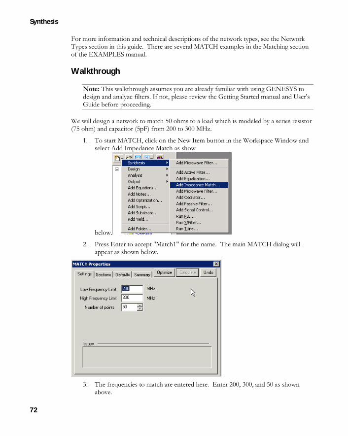
Synthesis
72
For more information and technical descriptions of the network types, see the Network Types section in this guide. There are several MATCH examples in the Matching section of the EXAMPLES manual.
Walkthrough
Note: This walkthrough assumes you are already familiar with using GENESYS to design and analyze filters. If not, please review the Getting Started manual and User's Guide before proceeding.
We will design a network to match 50 ohms to a load which is modeled by a series resistor (75 ohm) and capacitor (5pF) from 200 to 300 MHz.
1. To start MATCH, click on the New Item button in the Workspace Window and select Add Impedance Match as show
below.
2. Press Enter to accept "Match1" for the name. The main MATCH dialog will appear as shown below.
3. The frequencies to match are entered here. Enter 200, 300, and 50 as shown
above.
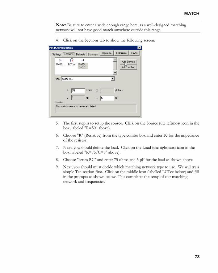
MATCH
73
Note: Be sure to enter a wide enough range here, as a well-designed matching network will not have good match anywhere outside this range.
4. Click on the Sections tab to show the following screen:
5. The first step is to setup the source. Click on the Source (the leftmost icon in the
box, labeled "R=50" above).
6. Choose "R" (Resistive) from the type combo box and enter 50 for the impedance of the resistor.
7. Next, you should define the load. Click on the Load (the rightmost icon in the box, labeled "R=75/C=5" above).
8. Choose "series RC" and enter 75 ohms and 5 pF for the load as shown above.
9. Next, you should must decide which matching network type to use. We will try a simple Tee section first. Click on the middle icon (labelled LCTee below) and fill in the prompts as shown below. This completes the setup of our matching network and frequencies.

Synthesis
74
10. Click the Calculate button in the upper left-corner of the dialog box. You should
see a synthesized tee network and its response as shown below.
Note: The series capacitor at the output is part of the load. The S11 and S22 magnitudes will be the same as if it were included in the load. It is not part of the circuit to be built.
11. This network is an ideal narrow-band tee network. For our application, we
should optimize it to increase the bandwidth (trading the depth of the notch for bandwidth). Click the Optimize button on the MATCH window. Let the
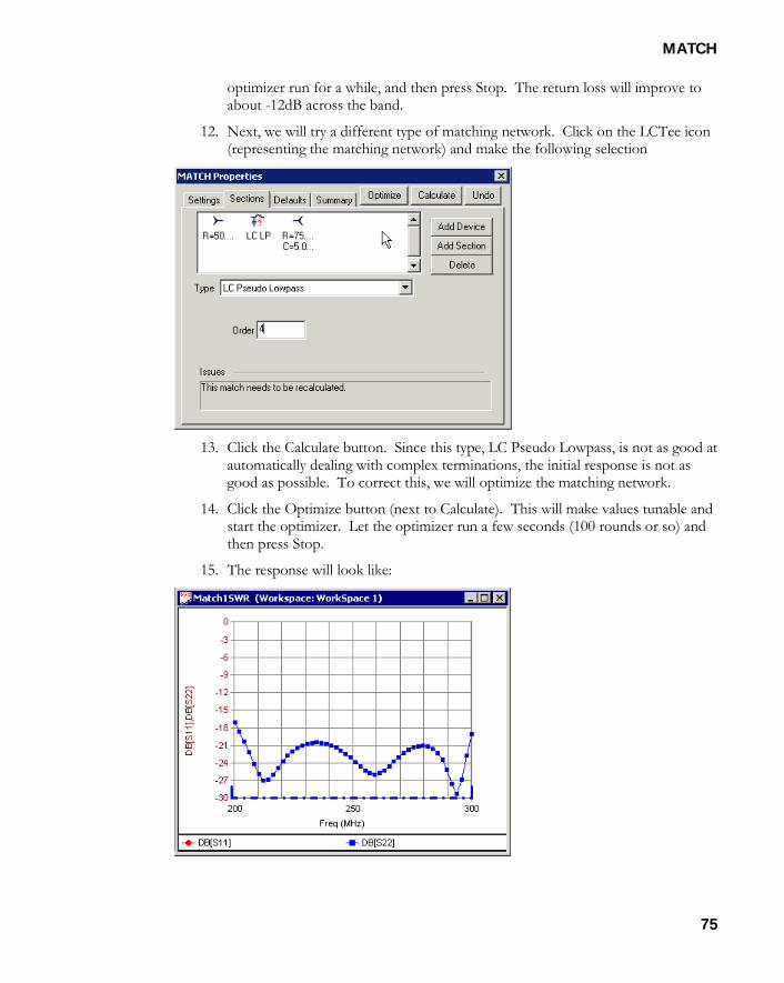
MATCH
75
optimizer run for a while, and then press Stop. The return loss will improve to about -12dB across the band.
12. Next, we will try a different type of matching network. Click on the LCTee icon (representing the matching network) and make the following selection
13. Click the Calculate button. Since this type, LC Pseudo Lowpass, is not as good at
automatically dealing with complex terminations, the initial response is not as good as possible. To correct this, we will optimize the matching network.
14. Click the Optimize button (next to Calculate). This will make values tunable and start the optimizer. Let the optimizer run a few seconds (100 rounds or so) and then press Stop.
15. The response will look like:
Synthesis
76
Generally, to design a matching network, you will want to follow a similar procedure: Try a matching network type and optimize it. If you don't like it, try a different one until you get the network and results you like.
Matching to device data There are several different ways to match to a device:
• For devices characterized by S-Parameter (S2P) files (e.g., linear transistors), you can match to the device data directly. You can match the input, output, and interstage networks simultaneously. See Matching\Unstable Device.wsx example for a walkthrough of matching to device data directly.
• For devices which require a schematic (e.g., stabilized devices, nonlinear devices, existing schematics), you can specify a 2-port network to match to. See the Matching\Unstable Device.wsx example for a walkthrough of matching devices on a schematic.
• For devices characterized only by impedance data (e.g., power transistors), you can specify the RX or S1P file for the source or load. See the Matching\Power Amp.wsx example for a walkthrough of matching to impedance data.
Unstable devices When the matching problem includes an S-parameter data file, MATCH tests the data for potential instability. Matching to a potentially unstable device is often mathematically unsuccessful or the resulting network might oscillate.
Matching a potentially unstable device is often unsuccessful. Even when successful, the resulting network might oscillate. If the stability warning appears, we recommend adding a network to the device to stabilize it before proceeding. You can use the "Stabilize Device" template for this purpose (choose File/New from Template).
See the Matching\Unstable Device.wsx example for a walkthrough of matching to unstable devices.
Custom Networks If you know the topology of the matching network you want to use, you can create a schematic with your network and specify that network to match to. See the Matching\Power Amp.wsx example for a walkthrough of using a custom network.
How MATCH Works Consider the following amplifier matching problem:
SOURCE [NETWORK] [DEVICE] [NETWORK] LOAD
In the first pass, MATCH uses a synthesis algorithm for the input network to match the source to the device S-parameter data. This synthesis may be exact or approximate, depending on the nature of the source, the network and the device.
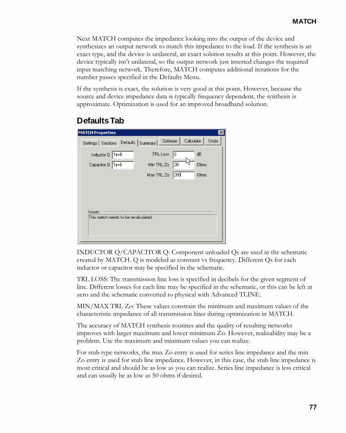
MATCH
77
Next MATCH computes the impedance looking into the output of the device and synthesizes an output network to match this impedance to the load. If the synthesis is an exact type, and the device is unilateral, an exact solution results at this point. However, the device typically isn’t unilateral, so the output network just inserted changes the required input matching network. Therefore, MATCH computes additional iterations for the number passes specified in the Defaults Menu.
If the synthesis is exact, the solution is very good at this point. However, because the source and device impedance data is typically frequency dependent, the synthesis is approximate. Optimization is used for an improved broadband solution.
Defaults Tab
INDUCTOR Q/CAPACITOR Q: Component unloaded Qs are used in the schematic created by MATCH. Q is modeled as constant vs frequency. Different Qs for each inductor or capacitor may be specified in the schematic.
TRL LOSS: The transmission line loss is specified in decibels for the given segment of line. Different losses for each line may be specified in the schematic, or this can be left at zero and the schematic converted to physical with Advanced TLINE.
MIN/MAX TRL Zo: These values constrain the minimum and maximum values of the characteristic impedance of all transmission lines during optimization in MATCH.
The accuracy of MATCH synthesis routines and the quality of resulting networks improves with larger maximum and lower minimum Zo. However, realizability may be a problem. Use the maximum and minimum values you can realize.
For stub type networks, the max Zo entry is used for series line impedance and the min Zo entry is used for stub line impedance. However, in this case, the stub line impedance is most critical and should be as low as you can realize. Series line impedance is less critical and can usually be as low as 50 ohms if desired.
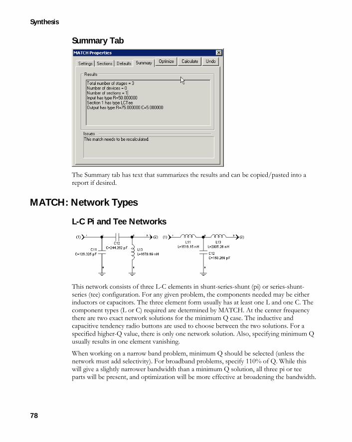
Synthesis
78
Summary Tab
The Summary tab has text that summarizes the results and can be copied/pasted into a report if desired.
MATCH: Network Types
L-C Pi and Tee Networks
This network consists of three L-C elements in shunt-series-shunt (pi) or series-shunt-series (tee) configuration. For any given problem, the components needed may be either inductors or capacitors. The three element form usually has at least one L and one C. The component types (L or C) required are determined by MATCH. At the center frequency there are two exact network solutions for the minimum Q case. The inductive and capacitive tendency radio buttons are used to choose between the two solutions. For a specified higher-Q value, there is only one network solution. Also, specifying minimum Q usually results in one element vanishing.
When working on a narrow band problem, minimum Q should be selected (unless the network must add selectivity). For broadband problems, specify 110% of Q. While this will give a slightly narrower bandwidth than a minimum Q solution, all three pi or tee parts will be present, and optimization will be more effective at broadening the bandwidth.
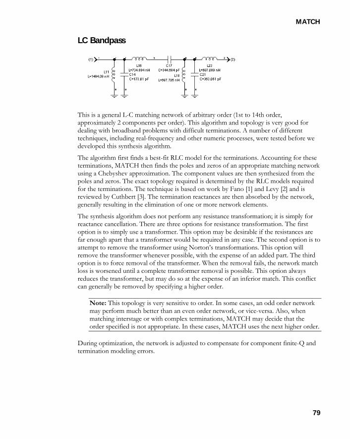
MATCH
79
LC Bandpass
This is a general L-C matching network of arbitrary order (1st to 14th order, approximately 2 components per order). This algorithm and topology is very good for dealing with broadband problems with difficult terminations. A number of different techniques, including real-frequency and other numeric processes, were tested before we developed this synthesis algorithm.
The algorithm first finds a best-fit RLC model for the terminations. Accounting for these terminations, MATCH then finds the poles and zeros of an appropriate matching network using a Chebyshev approximation. The component values are then synthesized from the poles and zeros. The exact topology required is determined by the RLC models required for the terminations. The technique is based on work by Fano [1] and Levy [2] and is reviewed by Cuthbert [3]. The termination reactances are then absorbed by the network, generally resulting in the elimination of one or more network elements.
The synthesis algorithm does not perform any resistance transformation; it is simply for reactance cancellation. There are three options for resistance transformation. The first option is to simply use a transformer. This option may be desirable if the resistances are far enough apart that a transformer would be required in any case. The second option is to attempt to remove the transformer using Norton’s transformations. This option will remove the transformer whenever possible, with the expense of an added part. The third option is to force removal of the transformer. When the removal fails, the network match loss is worsened until a complete transformer removal is possible. This option always reduces the transformer, but may do so at the expense of an inferior match. This conflict can generally be removed by specifying a higher order.
Note: This topology is very sensitive to order. In some cases, an odd order network may perform much better than an even order network, or vice-versa. Also, when matching interstage or with complex terminations, MATCH may decide that the order specified is not appropriate. In these cases, MATCH uses the next higher order.
During optimization, the network is adjusted to compensate for component finite-Q and termination modeling errors.

Synthesis
80
LC Pseudo Lowpass
This network is an L-C matching network with alternating shunt capacitors and series inductors (1st to 14th order, approximately 2 components per order). The match vanishes at DC, as for all networks without a transformer.
This algorithm has some aspects in common with the bandpass algorithm. First, the terminations are modeled as series RL or parallel RC. The poles and zeroes for a lowpass Chebyshev structure are found. These poles and zeros are transformed to pseudo-bandpass using a method described by Cotte and Joines [4] and enhanced significantly by Eagleware. This transformation results in the standard doubling of the number of poles and zeros. As a plus, this transformation to bandpass deals with unequal termination resistances so that a transformer is never required. A disadvantage of this network type is that the automatic modeling used for the terminations are much simpler than those used for the bandpass network, resulting in poorer initial match for some complex terminations. However, this problem is generally corrected during optimization.
TRL 1/4 Wave
This network contains a single series transmission line. This network is very good for narrowband matching of resistive terminations and can replace a transformer when broad bandwidth is not required. This network also has some capacity for dealing with complex terminations.
TRL Single/Double Stub
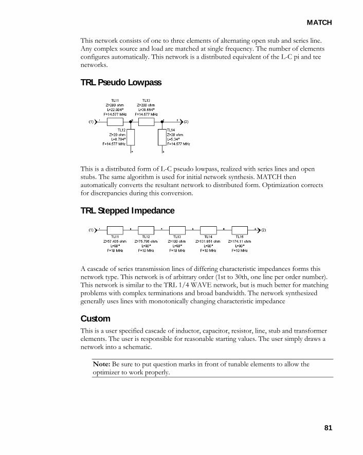
MATCH
81
This network consists of one to three elements of alternating open stub and series line. Any complex source and load are matched at single frequency. The number of elements configures automatically. This network is a distributed equivalent of the L-C pi and tee networks.
TRL Pseudo Lowpass
This is a distributed form of L-C pseudo lowpass, realized with series lines and open stubs. The same algorithm is used for initial network synthesis. MATCH then automatically converts the resultant network to distributed form. Optimization corrects for discrepancies during this conversion.
TRL Stepped Impedance
A cascade of series transmission lines of differing characteristic impedances forms this network type. This network is of arbitrary order (1st to 30th, one line per order number). This network is similar to the TRL 1/4 WAVE network, but is much better for matching problems with complex terminations and broad bandwidth. The network synthesized generally uses lines with monotonically changing characteristic impedance
Custom This is a user specified cascade of inductor, capacitor, resistor, line, stub and transformer elements. The user is responsible for reasonable starting values. The user simply draws a network into a schematic.
Note: Be sure to put question marks in front of tunable elements to allow the optimizer to work properly.

83
Chapter 6: MIXER
MIXER: Operation
Operation Overview
The MIXER Synthesis Module assists in the design of various types of mixers. The 11 topologies presented can be used as starting points for synthesis and analysis of mixers for a wide range of applications. These topologies can easily be modified to meet particular requirements and constraints. The synthesis module is integrated into the GENESYS environment, which allows an extensive number of analysis tools to be employed. This is particularly important in the design of mixers, where the nonlinear elements are an essential part of any configuration. The Harmonic Balance (HARBEC) nonlinear analysis tool, parameter sweeps, optimization and large signal s-parameter measurements are just a few of the features which can expedite the design process.
The following are the 11 mixer configurations available. The designs employ generic models for the nonlinear and active devices. These can easily be replaced with a model from one of the many libraries of commercially available parts.
1. Diode Single Ended Basic
2. Bipolar Differential
3. JFET Transformer Single Balanced
4. Diode Branch Line Single Balanced
5. Diode Transformer Single Balanced
6. JFET Single Ended
7. Diode Transformer Double Balanced
8. Bipolar Single Ended
9. Bipolar Transformer Single Balanced
10. Bipolar Double Balanced Gilbert
11. Diode Rat Race Single Balanced
The following sections include a walkthrough of the basic module operation, a description of the steps to change nonlinear device models, a description of outputs and settings, and a list of error messages.
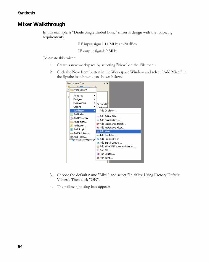
Synthesis
84
Mixer Walkthrough In this example, a "Diode Single Ended Basic" mixer is design with the following requirements:
RF input signal: 14 MHz at -20 dBm
IF output signal: 9 MHz
To create this mixer:
1. Create a new workspace by selecting "New" on the File menu.
2. Click the New Item button in the Workspace Window and select "Add Mixer" in the Synthesis submenu, as shown below.
3. Choose the default name "Mix1" and select "Initialize Using Factory Default Values". Then click "OK".
4. The following dialog box appears:
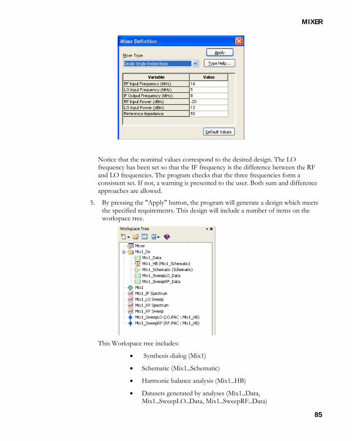
MIXER
85
Notice that the nominal values correspond to the desired design. The LO frequency has been set so that the IF frequency is the difference between the RF and LO frequencies. The program checks that the three frequencies form a consistent set. If not, a warning is presented to the user. Both sum and difference approaches are allowed.
5. By pressing the "Apply" button, the program will generate a design which meets the specified requirements. This design will include a number of items on the workspace tree.
This Workspace tree includes:
• Synthesis dialog (Mix1)
• Schematic (Mix1_Schematic)
• Harmonic balance analysis (Mix1_HB)
• Datasets generated by analyses (Mix1_Data, Mix1_SweepLO_Data, Mix1_SweepRF_Data)
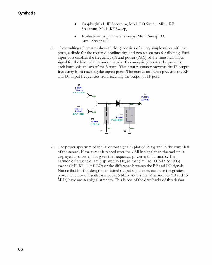
Synthesis
86
• Graphs (Mix1_IF Spectrum, Mix1_LO Sweep, Mix1_RF Spectrum, Mix1_RF Sweep)
• Evaluations or parameter sweeps (Mix1_SweepLO, Mix1_SweepRF)
6. The resulting schematic (shown below) consists of a very simple mixer with tree ports, a diode for the required nonlinearity, and two resonators for filtering. Each input port displays the frequency (F) and power (PAC) of the sinusoidal input signal for the harmonic balance analysis. This analysis generates the power in each harmonic at each of the 3 ports. The input resonator prevents the IF output frequency from reaching the inputs ports. The output resonator prevents the RF and LO input frequencies from reaching the output or IF port.
7. The power spectrum of the IF output signal is plotted in a graph in the lower left
of the screen. If the cursor is placed over the 9 MHz signal then the tool tip is displayed as shown. This gives the frequency, power and harmonic. The harmonic frequencies are displayed in Hz, so that (1* 1.4e+007-1* 5e+006) means (1*F_RF - 1 * f_LO) or the difference between the RF and LO signals. Notice that for this design the desired output signal does not have the greatest power. The Local Oscillator input at 5 MHz and its first 2 harmonics (10 and 15 MHz) have greater signal strength. This is one of the drawbacks of this design.
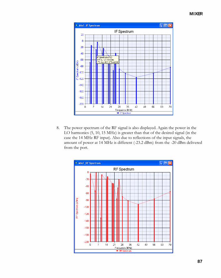
MIXER
87
8. The power spectrum of the RF signal is also displayed. Again the power in the LO harmonics (5, 10, 15 MHz) is greater than that of the desired signal (in the case the 14 MHz RF input). Also due to reflections of the input signals, the amount of power at 14 MHz is different (-23.2 dBm) from the -20 dBm delivered from the port.
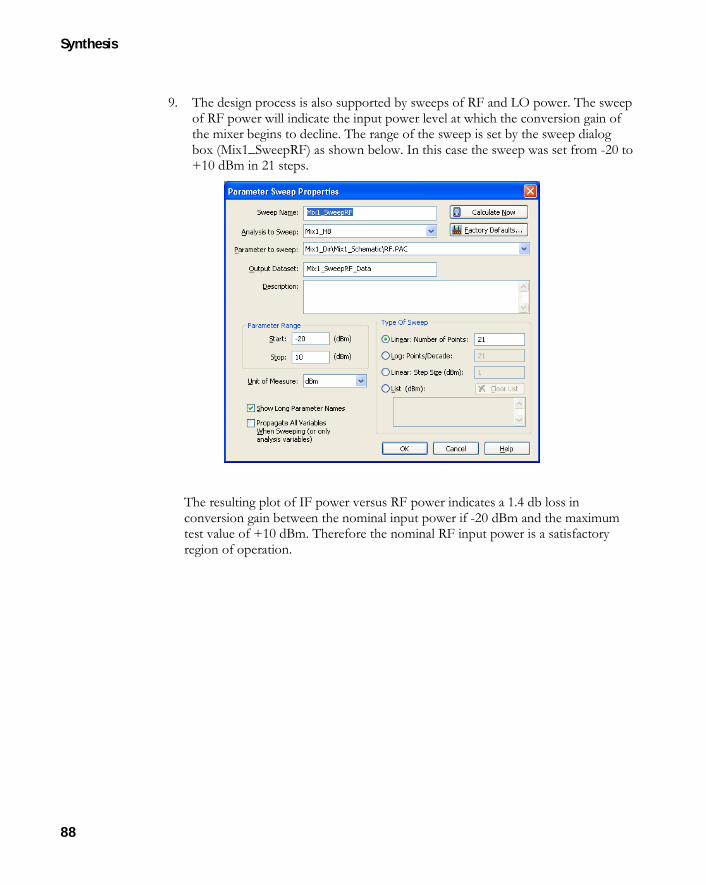
Synthesis
88
9. The design process is also supported by sweeps of RF and LO power. The sweep of RF power will indicate the input power level at which the conversion gain of the mixer begins to decline. The range of the sweep is set by the sweep dialog box (Mix1_SweepRF) as shown below. In this case the sweep was set from -20 to +10 dBm in 21 steps.
The resulting plot of IF power versus RF power indicates a 1.4 db loss in conversion gain between the nominal input power if -20 dBm and the maximum test value of +10 dBm. Therefore the nominal RF input power is a satisfactory region of operation.
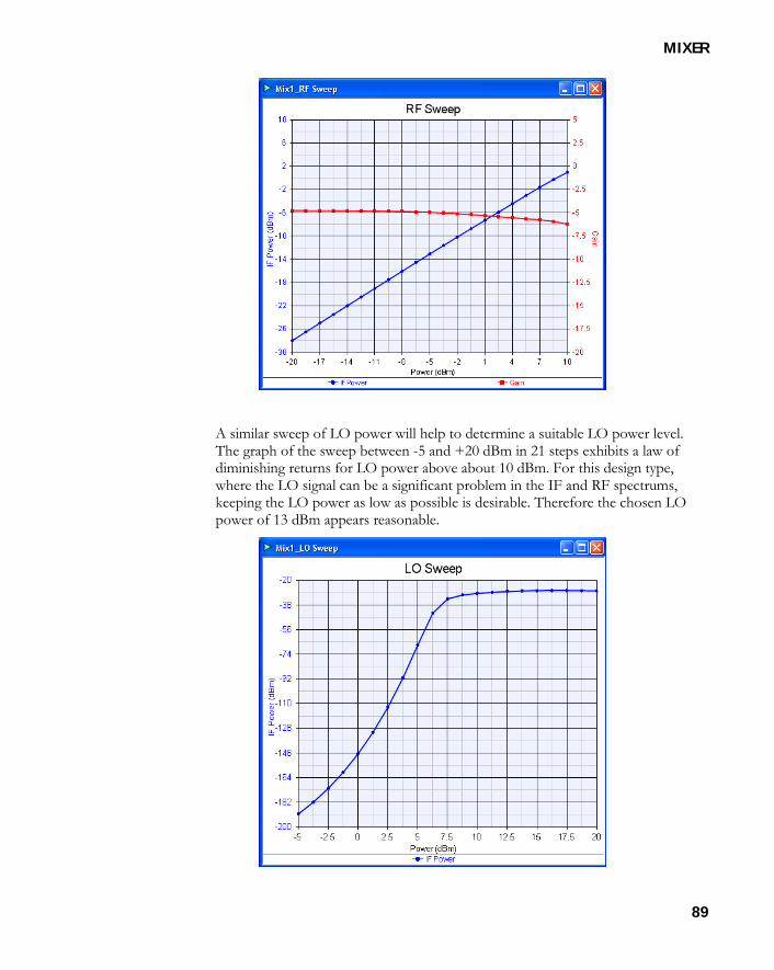
MIXER
89
A similar sweep of LO power will help to determine a suitable LO power level. The graph of the sweep between -5 and +20 dBm in 21 steps exhibits a law of diminishing returns for LO power above about 10 dBm. For this design type, where the LO signal can be a significant problem in the IF and RF spectrums, keeping the LO power as low as possible is desirable. Therefore the chosen LO power of 13 dBm appears reasonable.
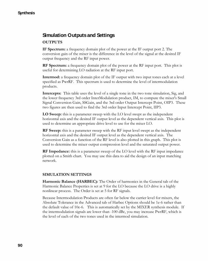
Synthesis
90
Simulation Outputs and Settings OUTPUTS IF Spectrum: a frequency domain plot of the power at the IF output port 2. The conversion gain of the mixer is the difference in the level of the signal at the desired IF output frequency and the RF input power.
RF Spectrum: a frequency domain plot of the power at the RF input port. This plot is useful for determining LO radiation at the RF input port.
Intermod: a frequency domain plot of the IF output with two input tones each at a level specified as PwrRF. This spectrum is used to determine the level of intermodulation products.
Intercepts: This table uses the level of a single tone in the two tone simulation, Sig, and the lower frequency 3rd order InterModulation product, IM, to compute the mixer's Small Signal Conversion Gain, SSGain, and the 3rd order Output Intercept Point, OIP3. These two figures are then used to find the 3rd order Input Intercept Point, IIP3.
LO Sweep: this is a parameter sweep with the LO level swept as the independent horizontal axis and the desired IF output level as the dependent vertical axis. This plot is used to determine an appropriate drive level to use for the mixer LO.
RF Sweep: this is a parameter sweep with the RF input level swept as the independent horizontal axis and the desired IF output level as the dependent vertical axis. The Conversion Gain as a function of the RF level is also plotted in this graph. This plot is used to determine the mixer output compression level and the saturated output power.
RF Impedance: this is a parameter sweep of the LO level with the RF input impedance plotted on a Smith chart. You may use this data to aid the design of an input matching network.
SIMULATION SETTINGS Harmonic Balance (HARBEC): The Order of harmonics in the General tab of the Harmonic Balance Properties is set at 9 for the LO because the LO drive is a highly nonlinear process. The Order is set at 5 for RF signals.
Because Intermodulation Products are often far below the carrier level for mixers, the Absolute Tolerance in the Advanced tab of Harbec Options should be 1e-6 rather than the default value of 10e-6. This is automatically set by the MIXER synthesis module. If the intermodulation signals are lower than -100 dBc, you may increase PwrRF, which is the level of each of the two tones used in the intermod simulation.
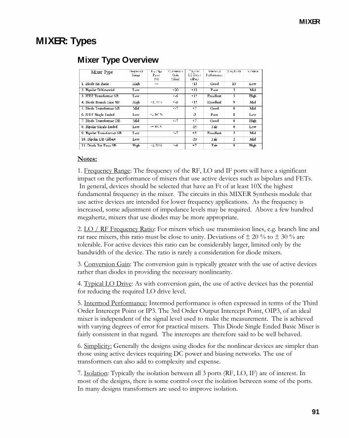
MIXER
91
MIXER: Types
Mixer Type Overview
Notes: 1. Frequency Range: The frequency of the RF, LO and IF ports will have a significant impact on the performance of mixers that use active devices such as bipolars and FETs. In general, devices should be selected that have an Ft of at least 10X the highest fundamental frequency in the mixer. The circuits in this MIXER Synthesis module that use active devices are intended for lower frequency applications. As the frequency is increased, some adjustment of impedance levels may be required. Above a few hundred megahertz, mixers that use diodes may be more appropriate.
2. LO / RF Frequency Ratio: For mixers which use transmission lines, e.g. branch line and rat race mixers, this ratio must be close to unity. Deviations of ± 20 % to ± 30 % are tolerable. For active devices this ratio can be considerably larger, limited only by the bandwidth of the device. The ratio is rarely a consideration for diode mixers.
3. Conversion Gain: The conversion gain is typically greater with the use of active devices rather than diodes in providing the necessary nonlinearity.
4. Typical LO Drive: As with conversion gain, the use of active devices has the potential for reducing the required LO drive level.
5. Intermod Performance: Intermod performance is often expressed in terms of the Third Order Intercept Point or IP3. The 3rd Order Output Intercept Point, OIP3, of an ideal mixer is independent of the signal level used to make the measurement. The is achieved with varying degrees of error for practical mixers. This Diode Single Ended Basic Mixer is fairly consistent in that regard. The intercepts are therefore said to be well behaved.
6. Simplicity: Generally the designs using diodes for the nonlinear devices are simpler than those using active devices requiring DC power and biasing networks. The use of transformers can also add to complexity and expense.
7. Isolation: Typically the isolation between all 3 ports (RF, LO, IF) are of interest. In most of the designs, there is some control over the isolation between some of the ports. In many designs transformers are used to improve isolation.
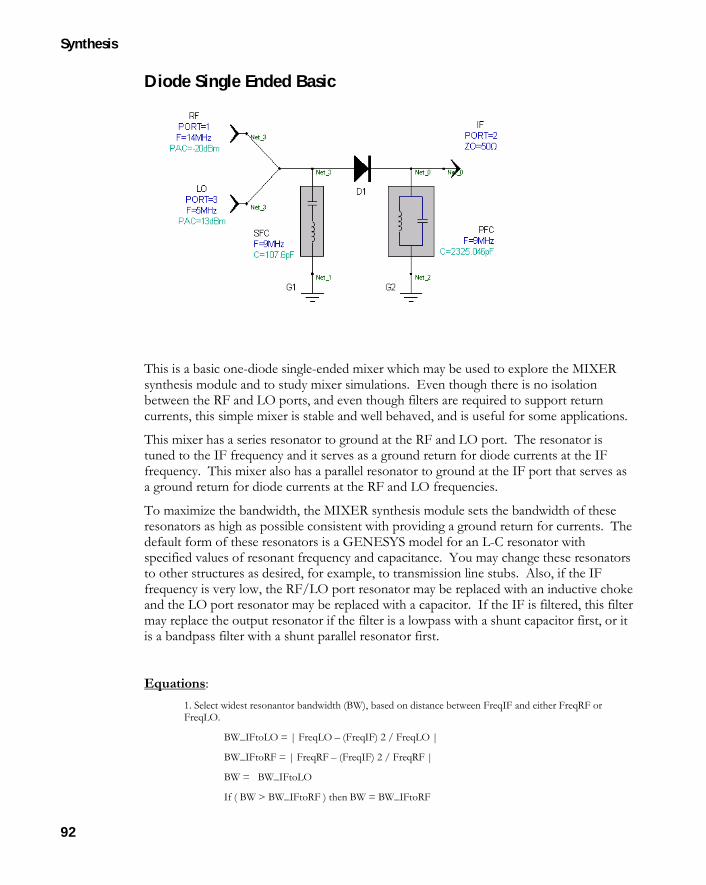
Synthesis
92
Diode Single Ended Basic
This is a basic one-diode single-ended mixer which may be used to explore the MIXER synthesis module and to study mixer simulations. Even though there is no isolation between the RF and LO ports, and even though filters are required to support return currents, this simple mixer is stable and well behaved, and is useful for some applications.
This mixer has a series resonator to ground at the RF and LO port. The resonator is tuned to the IF frequency and it serves as a ground return for diode currents at the IF frequency. This mixer also has a parallel resonator to ground at the IF port that serves as a ground return for diode currents at the RF and LO frequencies.
To maximize the bandwidth, the MIXER synthesis module sets the bandwidth of these resonators as high as possible consistent with providing a ground return for currents. The default form of these resonators is a GENESYS model for an L-C resonator with specified values of resonant frequency and capacitance. You may change these resonators to other structures as desired, for example, to transmission line stubs. Also, if the IF frequency is very low, the RF/LO port resonator may be replaced with an inductive choke and the LO port resonator may be replaced with a capacitor. If the IF is filtered, this filter may replace the output resonator if the filter is a lowpass with a shunt capacitor first, or it is a bandpass filter with a shunt parallel resonator first.
Equations: 1. Select widest resonantor bandwidth (BW), based on distance between FreqIF and either FreqRF or FreqLO.
BW_IFtoLO = | FreqLO – (FreqIF) 2 / FreqLO |
BW_IFtoRF = | FreqRF – (FreqIF) 2 / FreqRF |
BW = BW_IFtoLO
If ( BW > BW_IFtoRF ) then BW = BW_IFtoRF

MIXER
93
QL = FreqIF / BW
2. Compute capacitor Cin of input resonator (SFC) with QL set for 3 times narrower bandwidth.
Cin = (1e12) / [ 2 * p * FreqIF * 1e6 * 3 * QL * Zo ] pF
3. Compute capacitor Cout of output resonator (PFC) with QL set for 6 times narrower bandwidth.
Cout = (1e12 * 6 * QL) / [ 2 * p * FreqIF * 1e6 * Zo ] pF
2. Bipolar Differential
This mixer uses a bipolar differential pair with an active current source. It does not have good intermod performance but it has excellent conversion gain, up to 20 dB at low frequencies, and good isolation from the LO to RF ports. There is only moderate isolation from the LO to IF port.
The bias network in this mixer is designed for discrete devices with ample supply current available. The bias networks are stiff with at least 1 milliamp in the resistor dividers. The transistors have a minimum of 2 volts Vce. The minimum supply voltage is 5 volts. For handheld applications with limited current and voltage you will want to redesign the bias networks. This bias network is not balanced with respect to the base of the differential transistors. The high values of resistance allow an unbalanced bias network, but improved isolation would be achieved with a truly balanced bias network.
Synthesis
94
Both the RF and IF are differential to enhance the gain. If transformers are not desired, this circuit may converted to single-ended at one or both ports. The initial transformer ratios step the RF port impedance up by a factor of two and the IF port impedance back down by a factor of two. These ratios impact the gain and intermod performance. The optimum ratio is a function of the desired gain, intermod performance and operating frequency. You are encouraged to investigate other ratios.
The frequency of the RF, LO and IF ports will have a significant impact on the performance of mixers that use active devices such as bipolars and FETs. In general, devices should be selected that have an Ft of at least 10X the highest fundamental frequency in the mixer. The MIXER module circuits that use active devices are intended for lower frequency applications. As the frequency is increased, some adjustment of impedance levels may be required. Above a few hundred megahertz, mixers that use diodes may be more appropriate.
Equations:
1. Compute inductances for transformer (modelled as mutually coupled coils).
LpriIF = (1e9 * 6 * Zo) / [ 2 * p * FreqIF * 1e6 ] nH
LsecIF = 2 * LpriIF nH
LpriRF = (1e9 * 6 * Zo) / [ 2 * p * FreqRF * 1e6 ] nH
LsecRF = LpriRF nH
2. Compute bipolar transistor biasing resistors:
R1= ( Vcc – 3.9 ) / (1.0e-3) in ohms
R5 = ( Vcc – 1.9) / (1.9e-3) in ohms

MIXER
95
3. JFET Transformer Single Balanced
This JFET single-balanced mixer has excellent LO to RF and LO to IF isolation. Typical conversion gain is -6 to -7 dBm. This mixer requires high LO drive, about +15 dBm from a 50 ohm source. However, it provides excellent intermod performance.
The transformers step the RF source impedance up and the output IF impedance back down by a factor of 4. You may find that other impedance ratios provide improved performance at some frequencies and with some devices.
The gate impedance that loads the LO drive is typically higher than 50 ohms. Lower LO drive may be used by using a transformer to step a 50 ohm LO up to a higher impedance, such as 200 ohms. Alternatively, for narrowband applications, the coupling capacitor C5 and the gate bias resistor R3 may be replaced with a shunt inductor to form a matching network to step the LO impedance up. Depending on the frequency range, the active device and the required intermod performance, +7 dBm LO drive may be sufficient.
This MIXER Synthesis module uses generic models for bipolar transistors and diodes. However, the J310 (plastic) and U310 (metal) JFETs available from a number of manufacturers work so well in this mixer that it was used as the model. It has high Idss, low noise and high gain through the UHF frequency range. If you choose, you may double click on the FETs in the schematic and select a different device.
The voltage drop across resistors R1 and R2 set the drain currents somewhat less than Idss of the JFETs. A nominal value of 180 ohms will work in most cases. They may be adjusted so that the drain current is a desired fraction of Idss. For applications requiring less control of the drain current, resistors R1 and R2 and the capacitors in parallel with them may not be needed. Resistor R4 provides additional bypassing effectiveness and is also optional.
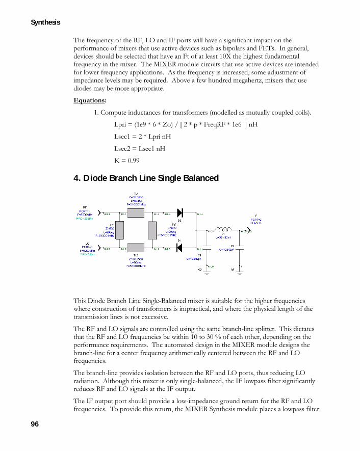
Synthesis
96
The frequency of the RF, LO and IF ports will have a significant impact on the performance of mixers that use active devices such as bipolars and FETs. In general, devices should be selected that have an Ft of at least 10X the highest fundamental frequency in the mixer. The MIXER module circuits that use active devices are intended for lower frequency applications. As the frequency is increased, some adjustment of impedance levels may be required. Above a few hundred megahertz, mixers that use diodes may be more appropriate.
Equations: 1. Compute inductances for transformers (modelled as mutually coupled coils).
Lpri = (1e9 * 6 * Zo) / [ 2 * p * FreqRF * 1e6 ] nH
Lsec1 = 2 * Lpri nH
Lsec2 = Lsec1 nH
K = 0.99
4. Diode Branch Line Single Balanced
This Diode Branch Line Single-Balanced mixer is suitable for the higher frequencies where construction of transformers is impractical, and where the physical length of the transmission lines is not excessive.
The RF and LO signals are controlled using the same branch-line splitter. This dictates that the RF and LO frequencies be within 10 to 30 % of each other, depending on the performance requirements. The automated design in the MIXER module designs the branch-line for a center frequency arithmetically centered between the RF and LO frequencies.
The branch-line provides isolation between the RF and LO ports, thus reducing LO radiation. Although this mixer is only single-balanced, the IF lowpass filter significantly reduces RF and LO signals at the IF output.
The IF output port should provide a low-impedance ground return for the RF and LO frequencies. To provide this return, the MIXER Synthesis module places a lowpass filter

MIXER
97
at the IF output with a shunt capacitor adjacent to the diodes. This filter is designed with a cutoff frequency equal to 1.25 times the specified IF frequency. For wide IF bandwidths, you may increase the cutoff frequency using the parameter in the dialog box and the program will automatically design this lowpass filter.
A lowpass filter assumes the IF is the difference of the RF and LO frequencies. For a sum mixer, you should replace the lowpass with a highpass or bandpass filter. This filter should also provide a low-impedance path to ground for the RF and LO frequencies.
The branch-line is designed with electrical models of the transmission lines. You may use the Advanced T/Line option to automatically convert the electrical lines into the line type of your choice, such as microstrip, stripline, etc.
Equations:
1. Compute parameters for electrical transmission line models (Length = 90 degrees).
FreqCenter = (FreqRF + FreqLO) / 2 + 0.01 in MHz 0.01 to improve convergence
Zseries = 0.7071 * Zo in ohms
Zshunt = Zo in ohms
2. Compute Low Pass Filter values for 3rd order filter with 20 dB passband ripple, corner frequency (fc) equal to 1.25 times FreqIF ( G-values: 0.8515, 1.1031)
fc = 1.25 * FreqIF fc is user input: “IF Filter Frequency (MHz)”
wc = 2 * p * fc * 1e6
C = (0.8515 * 1e12) / (wc * Zo) pF
L = (1.1031 * Zo * 1e9) / wc nH
5. Diode Transformer Single Balanced
Synthesis
98
This single balanced mixer offers isolation either between the LO and the IF port, or between the RF and the IF port, not both. The configuration synthesized here offers isolation between the RF and IF port. If isolation is desired between the LO and IF port, the RF and LO ports in the schematic may be switched. Because double balanced mixers offers isolation among all ports, they are more common. The primary advantage of the single balanced mixer is lower cost: two diodes and a transformer are saved. The theory of diode single balanced mixers is covered in the book "Radio Receiver Design" by Kevin McClaning and Tom Vito.
An inherent advantage of this mixer is broad bandwidth, limited primarily by the available bandwidth of the transformers. When wound as multifilar transmission line transformers, bandwidths of more than two decades are possible. In this way, one general purpose design may serve many applications. For information on the physical realization of these transformers you may refer to the book "Transmission Line Transformers" by Jerry Sevick.
This mixer exhibits a conversion loss of about 7 dB. In the normal form with a pair of diodes the nominal LO drive is about +7 dBm. These mixers exhibit good intermod performance. Multiple diodes may be used in series in each branch to increase the intermod performance. This requires higher LO drive levels. The typical output 3rd order intermodulation intercept point is roughly equal to the LO drive level.
These mixers work well when terminated in 50 ohms. In fact, for best intermod performance, the IF port in particular should be terminated with an excellent match to 50 ohms at all frequencies. Rather than terminating the output with an IF filter that is reactive at the RF and LO frequencies, for best intermod performance this mixer is terminated with a broadband amplifier with good return loss, or with a diplexer that passes the IF and terminates the RF and LO frequencies.
The default model is the built-in non-linear diode model. This mixer often uses hot-carrier diodes, but high-speed silicon diodes may be used as well.
Equations: 1. Compute inductances for transformers (modelled as mutually coupled coils).
Freq_XFMR = FreqRF
if ( FreqLO < FreqRF) then Freq_XFMR = FreqLO
Lpri = (1e9 * 6 * Zo) / [ 2 * p * Freq_XFMR * 1e6 ] nH
Lsec1 = Lpri / 2 nH
Lsec2 = Lsec1 nH
K = 0.99
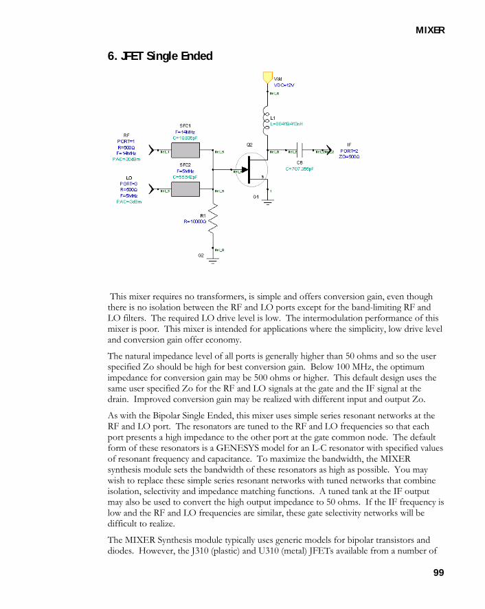
MIXER
99
6. JFET Single Ended
This mixer requires no transformers, is simple and offers conversion gain, even though there is no isolation between the RF and LO ports except for the band-limiting RF and LO filters. The required LO drive level is low. The intermodulation performance of this mixer is poor. This mixer is intended for applications where the simplicity, low drive level and conversion gain offer economy.
The natural impedance level of all ports is generally higher than 50 ohms and so the user specified Zo should be high for best conversion gain. Below 100 MHz, the optimum impedance for conversion gain may be 500 ohms or higher. This default design uses the same user specified Zo for the RF and LO signals at the gate and the IF signal at the drain. Improved conversion gain may be realized with different input and output Zo.
As with the Bipolar Single Ended, this mixer uses simple series resonant networks at the RF and LO port. The resonators are tuned to the RF and LO frequencies so that each port presents a high impedance to the other port at the gate common node. The default form of these resonators is a GENESYS model for an L-C resonator with specified values of resonant frequency and capacitance. To maximize the bandwidth, the MIXER synthesis module sets the bandwidth of these resonators as high as possible. You may wish to replace these simple series resonant networks with tuned networks that combine isolation, selectivity and impedance matching functions. A tuned tank at the IF output may also be used to convert the high output impedance to 50 ohms. If the IF frequency is low and the RF and LO frequencies are similar, these gate selectivity networks will be difficult to realize.
The MIXER Synthesis module typically uses generic models for bipolar transistors and diodes. However, the J310 (plastic) and U310 (metal) JFETs available from a number of
Synthesis
100
manufacturers work so well in this mixer that it was used as the model. It has high Idss, low noise and good gain through the VHF frequency range. If you choose, you may double click on the FETs in the schematic and select a different device.
The bias network is exceptionally simple. The source voltage is zero and the gate voltage is near zero. The drain current then becomes the Idss of the device. If desired, the drain current may be reduced by placing a resistor in series with the source. This resistor should be bypassed to retain a low LO drive level.
The frequency of the RF, LO and IF ports will have a significant impact on the performance of mixers that use active devices such as bipolars and FETs. In general, devices should be selected that have an Ft of at least 10X the highest fundamental frequency in the mixer. The MIXER module circuits that use active devices are intended for lower frequency applications. As the frequency is increased, some adjustment of impedance levels may be required. Above a few hundred megahertz, mixers that use diodes may be more appropriate.
The frequency of the RF, LO and IF ports will have a significant impact on the performance of mixers that use active devices such as bipolars and FETs. In general, devices should be selected that have an Ft of at least 10X the highest fundamental frequency in the mixer. The MIXER module circuits that use active devices are intended for lower frequency applications. As the frequency is increased, some adjustment of impedance levels may be required. Above a few hundred megahertz, mixers that use diodes may be more appropriate.
Equations: 1. Select widest resonator bandwidth (BW), based on distance between FreqRF and FreqLO
BW = | FreqRF – (FreqLO) 2 / FreqRF| in MHz
QL = FreqRF / BW
2. Compute capacitors of input resonators (SFC).
Crf = (1e12) / [ 2 * p * FreqRF * 1e6 * QL * Zo ] pF
Clo = (1e12) / [ 2 * p * FreqLO * 1e6 * QL * Zo ] pF
3. Compute elements of output network.
Ld = (1e9 * 10 * Zo) / [ 2 * p * FreqIF * 1e6 ] nH
Co = (1e12 ) / [ 0.05 * Zo * 2 * p * FreqIF * 1e6] pF
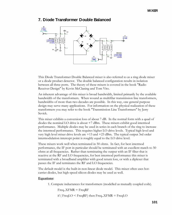
MIXER
101
7. Diode Transformer Double Balanced
This Diode Transformer Double Balanced mixer is also referred to as a ring diode mixer or a diode product detector. The double balanced configuration results in isolation between all three ports. The theory of these mixers is covered in the book "Radio Receiver Design" by Kevin McClaning and Tom Vito.
An inherent advantage of this mixer is broad bandwidth, limited primarily by the available bandwidth of the transformers. When wound as multifilar transmission line transformers, bandwidths of more than two decades are possible. In this way, one general purpose design may serve many applications. For information on the physical realization of these transformers you may refer to the book "Transmission Line Transformers" by Jerry Sevick.
This mixer exhibits a conversion loss of about 7 dB. In the normal form with a quad of diodes the nominal LO drive is about +7 dBm. These mixers exhibit good intermod performance. Multiple diodes may be used in series in each branch of the ring to increase the intermod performance. This requires higher LO drive levels. Typical high level and very high level mixer drive levels are +13 and +23 dBm. The typical output 3rd order intermodulation intercept point is roughly equal to the LO drive level.
These mixers work well when terminated in 50 ohms. In fact, for best intermod performance, the IF port in particular should be terminated with an excellent match to 50 ohms at all frequencies. Rather than terminating the output with an IF filter that is reactive at the RF and LO frequencies, for best intermod performance this mixer is terminated with a broadband amplifier with good return loss, or with a diplexer that passes the IF and terminates the RF and LO frequencies.
The default model is the built-in non-linear diode model. This mixer often uses hot-carrier diodes, but high-speed silicon diodes may be used as well.
Equations: 1. Compute inductances for transformers (modelled as mutually coupled coils).
Freq_XFMR = FreqRF
if ( FreqLO < FreqRF) then Freq_XFMR = FreqLO
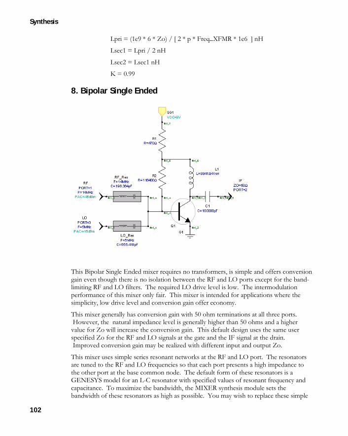
Synthesis
102
Lpri = (1e9 * 6 * Zo) / [ 2 * p * Freq_XFMR * 1e6 ] nH
Lsec1 = Lpri / 2 nH
Lsec2 = Lsec1 nH
K = 0.99
8. Bipolar Single Ended
This Bipolar Single Ended mixer requires no transformers, is simple and offers conversion gain even though there is no isolation between the RF and LO ports except for the band-limiting RF and LO filters. The required LO drive level is low. The intermodulation performance of this mixer only fair. This mixer is intended for applications where the simplicity, low drive level and conversion gain offer economy.
This mixer generally has conversion gain with 50 ohm terminations at all three ports. However, the natural impedance level is generally higher than 50 ohms and a higher value for Zo will increase the conversion gain. This default design uses the same user specified Zo for the RF and LO signals at the gate and the IF signal at the drain. Improved conversion gain may be realized with different input and output Zo.
This mixer uses simple series resonant networks at the RF and LO port. The resonators are tuned to the RF and LO frequencies so that each port presents a high impedance to the other port at the base common node. The default form of these resonators is a GENESYS model for an L-C resonator with specified values of resonant frequency and capacitance. To maximize the bandwidth, the MIXER synthesis module sets the bandwidth of these resonators as high as possible. You may wish to replace these simple
MIXER
103
series resonant networks with tuned networks that combine isolation, selectivity and impedance matching functions. A tuned tank at the IF output may also be used to match the output impedance. If the IF frequency is low and the RF and LO frequencies are similar, the base selectivity networks will be difficult to realize.
The default bias network is simple and guarantees the transistor is biased in the active region. It provides for Ic = 5 mA and a transistor beta of 100. For more critical applications, a more complex bias network with improved bias stability may be desired.
The frequency of the RF, LO and IF ports will have a significant impact on the performance of mixers that use active devices such as bipolars and FETs. In general, devices should be selected that have an Ft of at least 10X the highest fundamental frequency in the mixer. The MIXER module circuits that use active devices are intended for lower frequency applications. As the frequency is increased, some adjustment of impedance levels may be required. Above a few hundred megahertz, mixers that use diodes may be more appropriate.
The frequency of the RF, LO and IF ports will have a significant impact on the performance of mixers that use active devices such as bipolars and FETs. In general, devices should be selected that have an Ft of at least 10X the highest fundamental frequency in the mixer. The MIXER module circuits that use active devices are intended for lower frequency applications. As the frequency is increased, some adjustment of impedance levels may be required. Above a few hundred megahertz, mixers that use diodes may be more appropriate.
Equations: 1. Select widest resonator bandwidth (BW), based on distance between FreqRF and FreqLO
BW = | FreqRF – (FreqLO) 2 / FreqRF| in MHz
QL = FreqRF / BW
2. Compute capacitors of input resonators (SFC).
Crf = (1e12) / [ 2 * p * FreqRF * 1e6 * QL * Zo ] pF
Clo = (1e12) / [ 2 * p * FreqLO * 1e6 * QL * Zo ] pF
3. Compute inductor of output network.
L1 = (1e9 * 10 * Zo) / [ 2 * p * FreqIF * 1e6 ] n
4. Compute load resistor (R2) for Ic = 5 mA assuming beta = 100, Vbe = 0.83
R2 = ( Vcc – 2.35 –0.83 ) / (Ic * 1e-3/ beta) in ohms
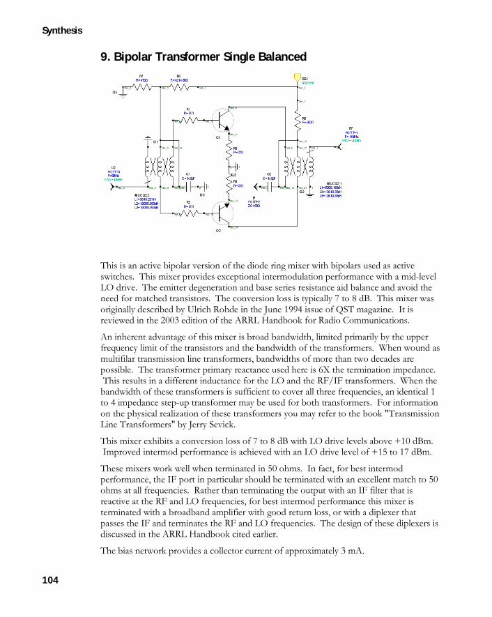
Synthesis
104
9. Bipolar Transformer Single Balanced
This is an active bipolar version of the diode ring mixer with bipolars used as active switches. This mixer provides exceptional intermodulation performance with a mid-level LO drive. The emitter degeneration and base series resistance aid balance and avoid the need for matched transistors. The conversion loss is typically 7 to 8 dB. This mixer was originally described by Ulrich Rohde in the June 1994 issue of QST magazine. It is reviewed in the 2003 edition of the ARRL Handbook for Radio Communications.
An inherent advantage of this mixer is broad bandwidth, limited primarily by the upper frequency limit of the transistors and the bandwidth of the transformers. When wound as multifilar transmission line transformers, bandwidths of more than two decades are possible. The transformer primary reactance used here is 6X the termination impedance. This results in a different inductance for the LO and the RF/IF transformers. When the bandwidth of these transformers is sufficient to cover all three frequencies, an identical 1 to 4 impedance step-up transformer may be used for both transformers. For information on the physical realization of these transformers you may refer to the book "Transmission Line Transformers" by Jerry Sevick.
This mixer exhibits a conversion loss of 7 to 8 dB with LO drive levels above +10 dBm. Improved intermod performance is achieved with an LO drive level of +15 to 17 dBm.
These mixers work well when terminated in 50 ohms. In fact, for best intermod performance, the IF port in particular should be terminated with an excellent match to 50 ohms at all frequencies. Rather than terminating the output with an IF filter that is reactive at the RF and LO frequencies, for best intermod performance this mixer is terminated with a broadband amplifier with good return loss, or with a diplexer that passes the IF and terminates the RF and LO frequencies. The design of these diplexers is discussed in the ARRL Handbook cited earlier.
The bias network provides a collector current of approximately 3 mA.

MIXER
105
The frequency of the RF, LO and IF ports will have a significant impact on the performance of mixers that use active devices such as bipolars and FETs. In general, devices should be selected that have an Ft of at least 10X the highest fundamental frequency in the mixer. The MIXER module circuits that use active devices are intended for lower frequency applications. Above a few hundred megahertz, mixers that use diodes may be more appropriate.
The frequency of the RF, LO and IF ports will have a significant impact on the performance of mixers that use active devices such as bipolars and FETs. In general, devices should be selected that have an Ft of at least 10X the highest fundamental frequency in the mixer. The MIXER module circuits that use active devices are intended for lower frequency applications. As the frequency is increased, some adjustment of impedance levels may be required. Above a few hundred megahertz, mixers that use diodes may be more appropriate.
Equations: 1. Compute inductances for transformers (modelled as mutually coupled coils).
L1pri = (1e9 * 6 * Zo) / [ 2 * p * FreqLO * 1e6 ] nH
L1sec = 2 * L1pri nH
Freq_low = FreqRF
if ( FreqIF < FreqRF) then Freq_low = FreqIF
L2pri = (1e9 * 6 * Zo) / [ 2 * p * Freq_low * 1e6 ] nH
L2sec = 2 * L2pri nH
K = 0.99
2. Compute bipolar transistor biasing and load resistors:
R6 = ( Vs – 0.95 ) / (1.91e-3) in ohms
R5 = Vs / (25e-3) in ohms

Synthesis
106
10. Bipolar Double Balanced Gilbert
This Bipolar Double Balanced Gilbert Cell mixer is sometimes referred two as a four-quadrant multiplier because when signals are "multiplied" their frequencies are mixed (as they are with all mixers). This mixer is realized using two differential transistor pairs that share a current source controlled by one of the input signals. The mixer was introduced in a paper by Barrie Gilbert in the December 1968 issue of the Journal of Solid State Circuits. This and the original mixer utilize bipolar devices. Today it is realized using virtually every type of active device.
In this implementation the differential current sources are driven by the RF signal using a transformer as a balun. The LO drive is also applied using a transformer and the IF output is taken with a transformer. In IC circuits the signals may, of course, remain balanced and transformers are not required.
The impedance level of all ports is generally higher than 50 ohms, particularly at lower frequency. The baluns may also serve as impedance transformers. The term Zo is the port impedance and the terms Zif, Zrf and Zlo in the equations below are factors that use the transformers to multiply the port impedance up to the internal impedances of the mixer. As the frequency is increased, optimum performance may result with lower factors. For information on the physical realization of these transformers you may refer to the book "Transmission Line Transformers" by Jerry Sevick.
This mixer exhibits conversion gain at frequencies where the device gain overcomes the loss associated with the mixing process. The differential pair transistors provide gain so the required LO drive level is low. Aided by the voltage step up resulting from the

MIXER
107
impedance transformation, and by the gain of the differential transistor pairs, the required LO drive is quite low, as low as -20 dBm at low frequencies.
The intermodulation performance of this mixer is only fair.
The bias network provides for approximately 2.5 mA in each current source and a Vce of at least 1.4 volts in each transistor. This requires a minimum supply voltage about 5 volts. Lower supply voltages are accommodated by redesigning the bias network.
The frequency of the RF, LO and IF ports will have a significant impact on the performance of mixers that use active devices such as bipolars and FETs. In general, devices should be selected that have an Ft of at least 10X the highest fundamental frequency in the mixer. The MIXER module circuits that use active devices are intended for lower frequency applications. Above a few hundred megahertz, mixers that use diodes may be more appropriate.
The frequency of the RF, LO and IF ports will have a significant impact on the performance of mixers that use active devices such as bipolars and FETs. In general, devices should be selected that have an Ft of at least 10X the highest fundamental frequency in the mixer. The circuits in this MIXER Synthesis module that use active devices are intended for lower frequency applications. As the frequency is increased, some adjustment of impedance levels may be required. Above a few hundred megahertz, mixers that use diodes may be more appropriate.
Equations:
1. Compute inductances for transformers (modelled as mutually coupled coils).
Zif = Zrf = Zlo = 8
LpriIF = (1e9 * 6 * Zo) / [ 2 * p * FreqIF * 1e6 ] nH
LsecIF = Zif * LpriIF nH
LpriRF = (1e9 * 6 * Zo) / [ 2 * p * FreqRF * 1e6 ] nH
LsecRF = Zrf * LpriRF nH
LpriLO = (1e9 * 6 * Zo) / [ 2 * p * FreqLO * 1e6 ] nH
LsecLO = Zlo * LpriLO nH
K = 0.99
2. Compute bipolar transistor biasing resistors:
R6 = ( Vs – 2.9 ) / (0.933e-3) in ohms
R7 = 1500 in ohms
R8 = 1500 in ohms
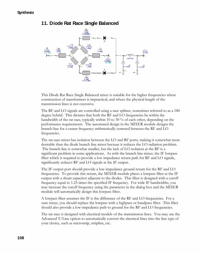
Synthesis
108
11. Diode Rat Race Single Balanced
This Diode Rat Race Single Balanced mixer is suitable for the higher frequencies where construction of transformers is impractical, and where the physical length of the transmission lines is not excessive.
The RF and LO signals are controlled using a race splitter, sometimes referred to as a 180 degree hybrid. This dictates that both the RF and LO frequencies be within the bandwidth of the rat race, typically within 10 to 30 % of each other, depending on the performance requirements. The automated design in the MIXER module designs the branch-line for a center frequency arithmetically centered between the RF and LO frequencies.
The rat-race mixer has isolation between the LO and RF ports, making it somewhat more desirable than the diode branch line mixer because it reduces the LO radiation problem. The branch-line is somewhat smaller, but the lack of LO isolation at the RF is a significant problem in some applications. As with the branch line mixer, the IF lowpass filter which is required to provide a low impedance return path for RF and LO signals, significantly reduces RF and LO signals at the IF output.
The IF output port should provide a low-impedance ground return for the RF and LO frequencies. To provide this return, the MIXER module places a lowpass filter at the IF output with a shunt capacitor adjacent to the diodes. This filter is designed with a cutoff frequency equal to 1.25 times the specified IF frequency. For wide IF bandwidths, you may increase the cutoff frequency using the parameter in the dialog box and the MIXER module will automatically design this lowpass filter.
A lowpass filter assumes the IF is the difference of the RF and LO frequencies. For a sum mixer, you should replace the lowpass with a highpass or bandpass filter. This filter should also provide a low-impedance path to ground for the RF and LO frequencies.
The rat-race is designed with electrical models of the transmission lines. You may use the Advanced T/Line option to automatically convert the electrical lines into the line type of your choice, such as microstrip, stripline, etc.
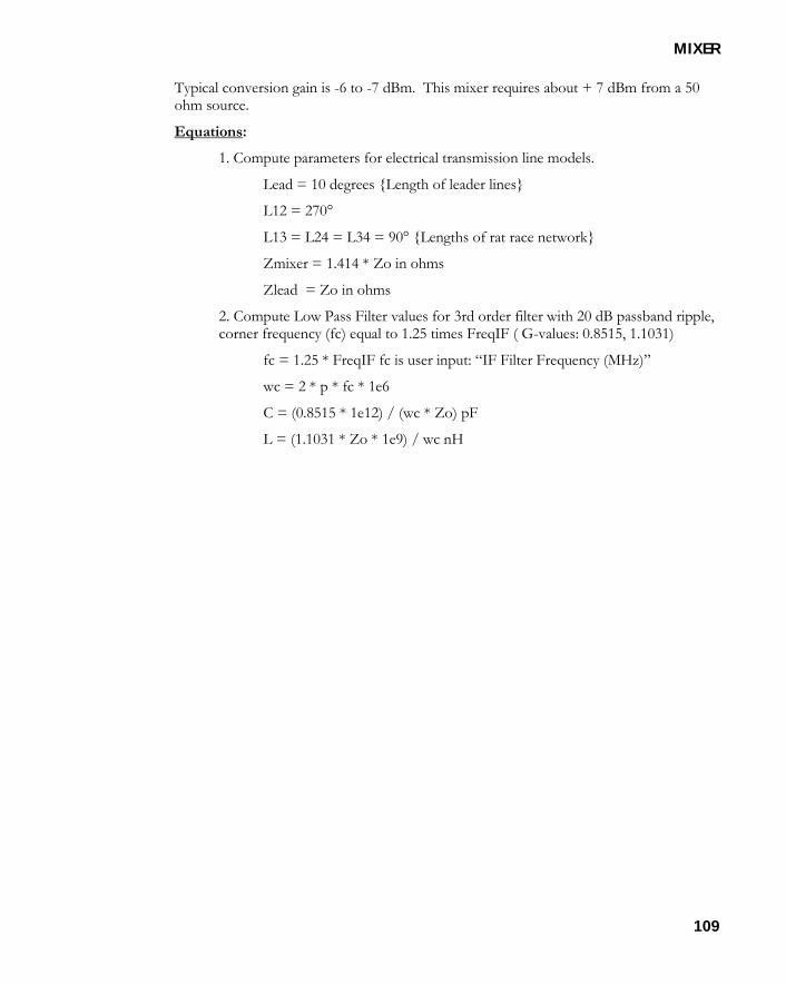
MIXER
109
Typical conversion gain is -6 to -7 dBm. This mixer requires about + 7 dBm from a 50 ohm source.
Equations: 1. Compute parameters for electrical transmission line models.
Lead = 10 degrees Length of leader lines
L12 = 270°
L13 = L24 = L34 = 90° Lengths of rat race network
Zmixer = 1.414 * Zo in ohms
Zlead = Zo in ohms
2. Compute Low Pass Filter values for 3rd order filter with 20 dB passband ripple, corner frequency (fc) equal to 1.25 times FreqIF ( G-values: 0.8515, 1.1031)
fc = 1.25 * FreqIF fc is user input: “IF Filter Frequency (MHz)”
wc = 2 * p * fc * 1e6
C = (0.8515 * 1e12) / (wc * Zo) pF
L = (1.1031 * Zo * 1e9) / wc nH

111
Chapter 7: M/FILTER
M/FILTER: Operation
Overview M/FILTER is the GENESYS synthesis module which designs microwave distributed filters. A feature of M/FILTER is the ability to absorb discontinuities during synthesis. Independent response calculation verifies the synthesis process.
Note: The book HF Filter Design and Computer Simulation also includes additional information on filter theory, elements and a variety of practical microwave filter structures.
The principal features of M/FILTER include:
• Lowpass, highpass, bandstop and a wide range of bandpass filter types
• Five different implementation processes including simple electrical, microstrip, stripline, slabline and coaxial.
• Full Integration with GENESYS environment
• Automatically displays layout or schematic on screen
• Allows specification of units, size and cross hairs for final board layout
Walkthrough The M/FILTER distributed filter synthesis module is integrated into the main GENESYS environment. All synthesis programs design circuits as prompt values are changed.
In this walkthrough, the following filter is designed:
• 50 Ω source and load terminations
• Chebyshev lowpass filter
• 0.25 dB of passband ripple
• 7th order
• 2 GHz cutoff frequency
• Stepped impedance configuration
• Microstrip
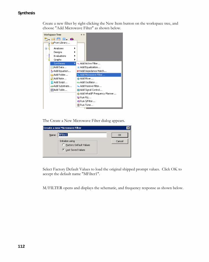
Synthesis
112
Create a new filter by right-clicking the New Item button on the workspace tree, and choose "Add Microwave Filter" as shown below.
The Create a New Microwave Filter dialog appears.
Select Factory Default Values to load the original shipped prompt values. Click OK to accept the default name "MFilter1".
M/FILTER opens and displays the schematic, and frequency response as shown below.
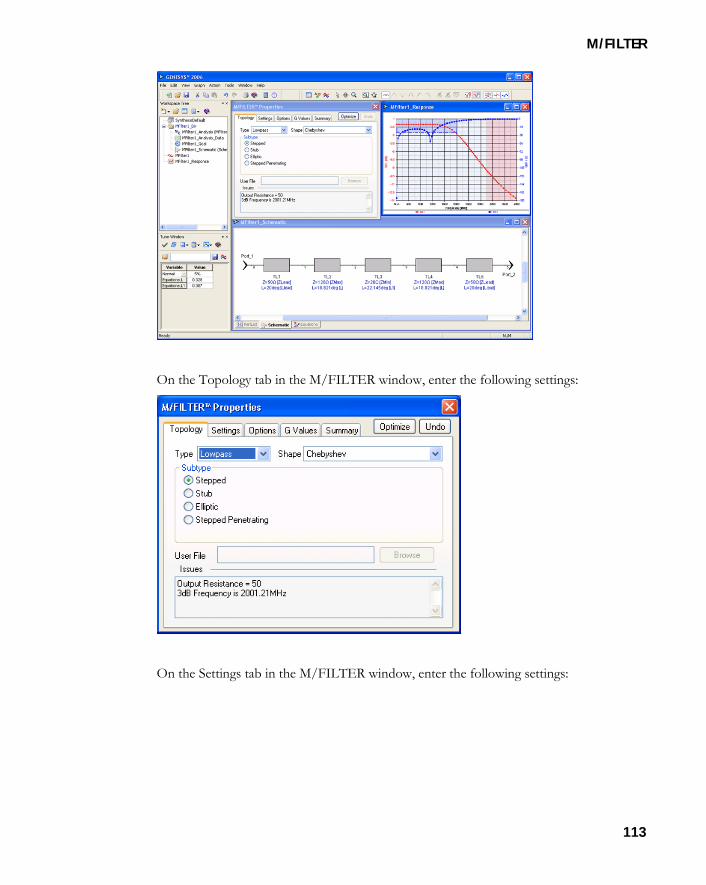
M/FILTER
113
On the Topology tab in the M/FILTER window, enter the following settings:
On the Settings tab in the M/FILTER window, enter the following settings:
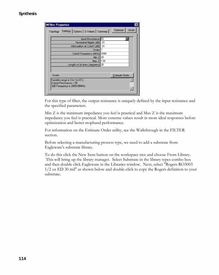
Synthesis
114
For this type of filter, the output resistance is uniquely defined by the input resistance and the specified parameters.
Min Z is the minimum impedance you feel is practical and Max Z is the maximum impedance you feel is practical. More extreme values result in more ideal responses before optimization and better stopband performance.
For information on the Estimate Order utility, see the Walkthrough in the FILTER section.
Before selecting a manufacturing process type, we need to add a substrate from Eagleware's substrate library.
To do this click the New Item button on the workspace tree and choose From Library. This will bring up the library manager. Select Substrate in the library types combo box and then double click Eagleware in the Libraries window. Next, select "Rogers RO3003 1/2 oz ED 30 mil" as shown below and double-click to copy the Rogers definition to your substrate.
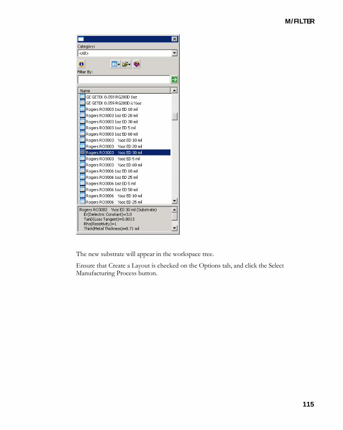
M/FILTER
115
The new substrate will appear in the workspace tree.
Ensure that Create a Layout is checked on the Options tab, and click the Select Manufacturing Process button.
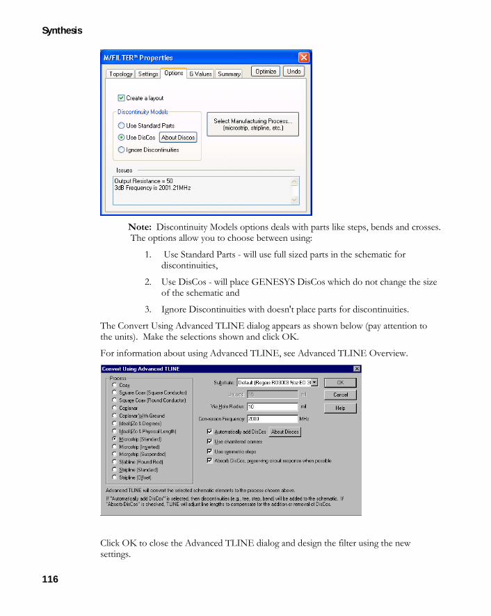
Synthesis
116
Note: Discontinuity Models options deals with parts like steps, bends and crosses. The options allow you to choose between using:
1. Use Standard Parts - will use full sized parts in the schematic for discontinuities,
2. Use DisCos - will place GENESYS DisCos which do not change the size of the schematic and
3. Ignore Discontinuities with doesn't place parts for discontinuities.
The Convert Using Advanced TLINE dialog appears as shown below (pay attention to the units). Make the selections shown and click OK.
For information about using Advanced TLINE, see Advanced TLINE Overview.
Click OK to close the Advanced TLINE dialog and design the filter using the new settings.
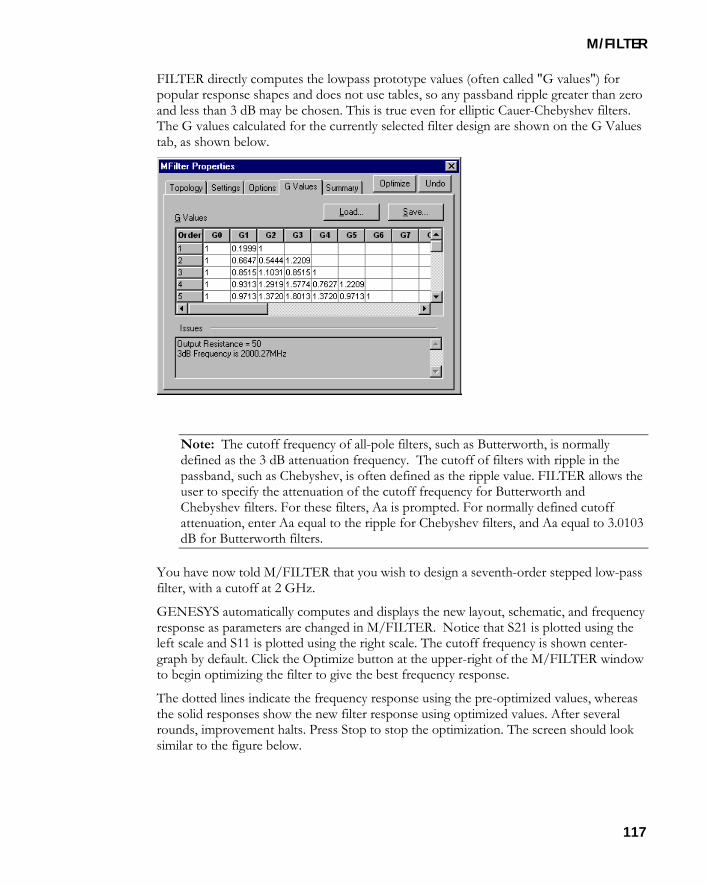
M/FILTER
117
FILTER directly computes the lowpass prototype values (often called "G values") for popular response shapes and does not use tables, so any passband ripple greater than zero and less than 3 dB may be chosen. This is true even for elliptic Cauer-Chebyshev filters. The G values calculated for the currently selected filter design are shown on the G Values tab, as shown below.
Note: The cutoff frequency of all-pole filters, such as Butterworth, is normally defined as the 3 dB attenuation frequency. The cutoff of filters with ripple in the passband, such as Chebyshev, is often defined as the ripple value. FILTER allows the user to specify the attenuation of the cutoff frequency for Butterworth and Chebyshev filters. For these filters, Aa is prompted. For normally defined cutoff attenuation, enter Aa equal to the ripple for Chebyshev filters, and Aa equal to 3.0103 dB for Butterworth filters.
You have now told M/FILTER that you wish to design a seventh-order stepped low-pass filter, with a cutoff at 2 GHz.
GENESYS automatically computes and displays the new layout, schematic, and frequency response as parameters are changed in M/FILTER. Notice that S21 is plotted using the left scale and S11 is plotted using the right scale. The cutoff frequency is shown center-graph by default. Click the Optimize button at the upper-right of the M/FILTER window to begin optimizing the filter to give the best frequency response.
The dotted lines indicate the frequency response using the pre-optimized values, whereas the solid responses show the new filter response using optimized values. After several rounds, improvement halts. Press Stop to stop the optimization. The screen should look similar to the figure below.
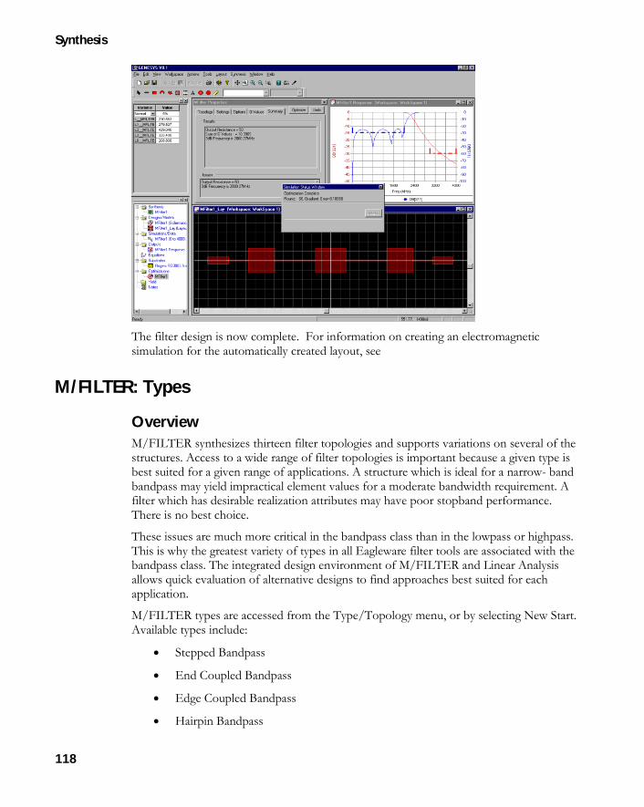
Synthesis
118
The filter design is now complete. For information on creating an electromagnetic simulation for the automatically created layout, see
M/FILTER: Types
Overview M/FILTER synthesizes thirteen filter topologies and supports variations on several of the structures. Access to a wide range of filter topologies is important because a given type is best suited for a given range of applications. A structure which is ideal for a narrow- band bandpass may yield impractical element values for a moderate bandwidth requirement. A filter which has desirable realization attributes may have poor stopband performance. There is no best choice.
These issues are much more critical in the bandpass class than in the lowpass or highpass. This is why the greatest variety of types in all Eagleware filter tools are associated with the bandpass class. The integrated design environment of M/FILTER and Linear Analysis allows quick evaluation of alternative designs to find approaches best suited for each application.
M/FILTER types are accessed from the Type/Topology menu, or by selecting New Start. Available types include:
• Stepped Bandpass
• End Coupled Bandpass
• Edge Coupled Bandpass
• Hairpin Bandpass
M/FILTER
119
• Combline Bandpass
• Interdigital Bandpass
• Elliptic Bandpass
• Quarterwave Coupled Bandpass
• Stepped Lowpass
• Stub Lowpass
• Elliptic Lowpass
• Stepped Penetrating Lowpass
• Stub Highpass
• Direct Coupled Bandstop
• Edge Coupled Bandstop
Filter Shapes and Processes M/FILTER supports numerous filter transfer approximation shapes and manufacturing processes. Transfer approximations are discussed in Appendix A . Available transfer functions are:
Elliptic • Cauer-Chebyshev, Normal Terminations
• Cauer-Chebyshev, Equal Terminations
• Elliptic Bessel
• Elliptic User File
All-Pole • Butterworth
• Chebyshev
• Bessel
• Transitional Gaussian to 6 and 12 dB
• Equiripple Phase Error of 0.05 and 0.5o
• Singly-Equalized
• Singly-Terminated Chebyshev
• Singly-Terminated Butterworth
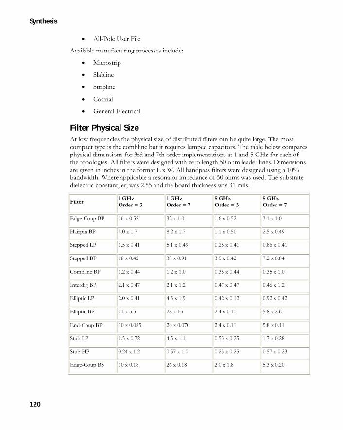
Synthesis
120
• All-Pole User File
Available manufacturing processes include:
• Microstrip
• Slabline
• Stripline
• Coaxial
• General Electrical
Filter Physical Size At low frequencies the physical size of distributed filters can be quite large. The most compact type is the combline but it requires lumped capacitors. The table below compares physical dimensions for 3rd and 7th order implementations at 1 and 5 GHz for each of the topologies. All filters were designed with zero length 50 ohm leader lines. Dimensions are given in inches in the format L x W. All bandpass filters were designed using a 10% bandwidth. Where applicable a resonator impedance of 50 ohms was used. The substrate dielectric constant, er, was 2.55 and the board thickness was 31 mils.
Filter 1 GHz Order = 3
1 GHz Order = 7
5 GHz Order = 3
5 GHz Order = 7
Edge-Coup BP 16 x 0.52 32 x 1.0 1.6 x 0.52 3.1 x 1.0
Hairpin BP 4.0 x 1.7 8.2 x 1.7 1.1 x 0.50 2.5 x 0.49
Stepped LP 1.5 x 0.41 5.1 x 0.49 0.25 x 0.41 0.86 x 0.41
Stepped BP 18 x 0.42 38 x 0.91 3.5 x 0.42 7.2 x 0.84
Combline BP 1.2 x 0.44 1.2 x 1.0 0.35 x 0.44 0.35 x 1.0
Interdig BP 2.1 x 0.47 2.1 x 1.2 0.47 x 0.47 0.46 x 1.2
Elliptic LP 2.0 x 0.41 4.5 x 1.9 0.42 x 0.12 0.92 x 0.42
Elliptic BP 11 x 5.5 28 x 13 2.4 x 0.11 5.8 x 2.6
End-Coup BP 10 x 0.085 26 x 0.070 2.4 x 0.11 5.8 x 0.11
Stub LP 1.5 x 0.72 4.5 x 1.1 0.53 x 0.25 1.7 x 0.28
Stub HP 0.24 x 1.2 0.57 x 1.0 0.25 x 0.25 0.57 x 0.23
Edge-Coup BS 10 x 0.18 26 x 0.18 2.0 x 1.8 5.3 x 0.20
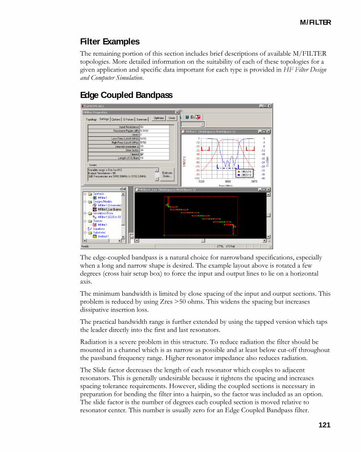
M/FILTER
121
Filter Examples The remaining portion of this section includes brief descriptions of available M/FILTER topologies. More detailed information on the suitability of each of these topologies for a given application and specific data important for each type is provided in HF Filter Design and Computer Simulation.
Edge Coupled Bandpass
The edge-coupled bandpass is a natural choice for narrowband specifications, especially when a long and narrow shape is desired. The example layout above is rotated a few degrees (cross hair setup box) to force the input and output lines to lie on a horizontal axis.
The minimum bandwidth is limited by close spacing of the input and output sections. This problem is reduced by using Zres >50 ohms. This widens the spacing but increases dissipative insertion loss.
The practical bandwidth range is further extended by using the tapped version which taps the leader directly into the first and last resonators.
Radiation is a severe problem in this structure. To reduce radiation the filter should be mounted in a channel which is as narrow as possible and at least below cut-off throughout the passband frequency range. Higher resonator impedance also reduces radiation.
The Slide factor decreases the length of each resonator which couples to adjacent resonators. This is generally undesirable because it tightens the spacing and increases spacing tolerance requirements. However, sliding the coupled sections is necessary in preparation for bending the filter into a hairpin, so the factor was included as an option. The slide factor is the number of degrees each coupled section is moved relative to resonator center. This number is usually zero for an Edge Coupled Bandpass filter.

Synthesis
122
Hairpin Bandpass
The hairpin bandpass is mathematically identical to the edge-coupled bandpass with a slide factor and bend discontinuities. Like the edge-coupled bandpass it is most suitable for narrowband applications. Spacing issues are similar to the edge-coupled. The practical bandwidth range is further extended by using the tapped version .
As the frequency is increased a higher resonator impedance is desirable. Folding reduces radiation significantly. Folding also saves considerable space at lower frequencies. Resonator self-coupling is avoided by separating hairpin arms by the greater of 3X the spacings or 5X the substrate thickness.
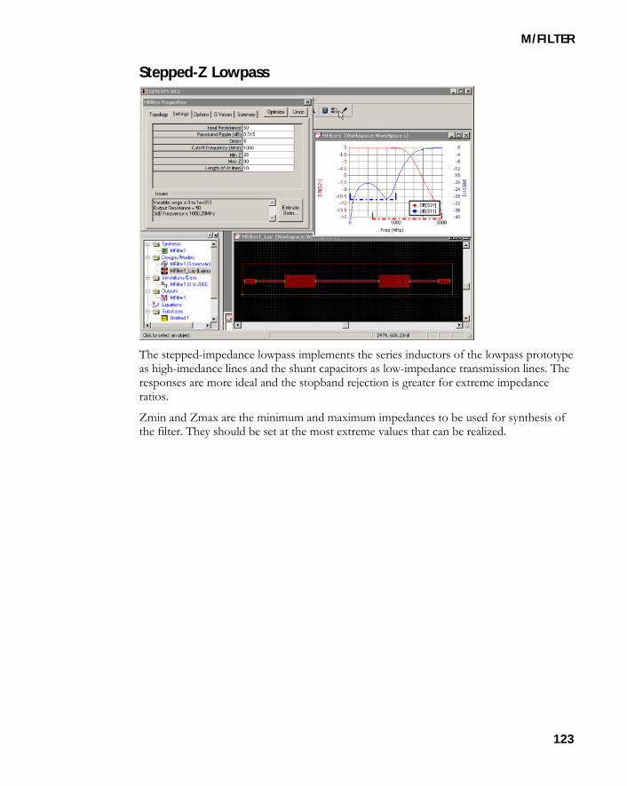
M/FILTER
123
Stepped-Z Lowpass
The stepped-impedance lowpass implements the series inductors of the lowpass prototype as high-imedance lines and the shunt capacitors as low-impedance transmission lines. The responses are more ideal and the stopband rejection is greater for extreme impedance ratios.
Zmin and Zmax are the minimum and maximum impedances to be used for synthesis of the filter. They should be set at the most extreme values that can be realized.
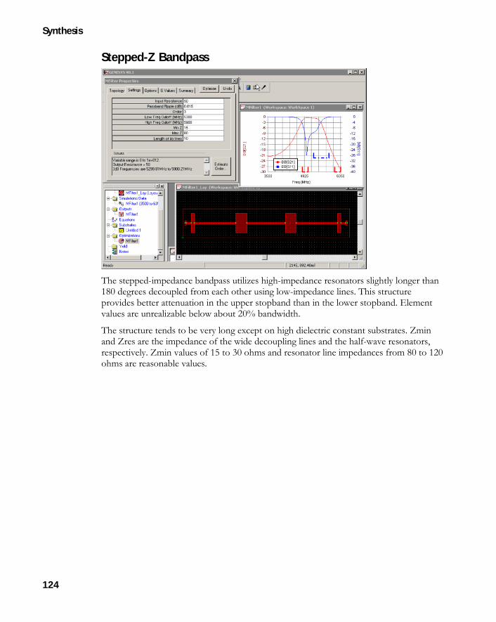
Synthesis
124
Stepped-Z Bandpass
The stepped-impedance bandpass utilizes high-impedance resonators slightly longer than 180 degrees decoupled from each other using low-impedance lines. This structure provides better attenuation in the upper stopband than in the lower stopband. Element values are unrealizable below about 20% bandwidth.
The structure tends to be very long except on high dielectric constant substrates. Zmin and Zres are the impedance of the wide decoupling lines and the half-wave resonators, respectively. Zmin values of 15 to 30 ohms and resonator line impedances from 80 to 120 ohms are reasonable values.

M/FILTER
125
Combline Bandpass
The combline bandpass is one of the most compact of all distributed filters. It is used in both printed planar and machined slabline. The air slabline version yields exceptional Qu so this structure is well suited for narrowband filters. It has excellent stopband performance which improves with shorter Res q, at the expense of Qu. Loading capacitors are required for each resonator, but this provides a means of tuning.
Zres is the impedance of the resonators and Res q is the phase length of the resonators which must be <90 and is typically 15<q<45. The above example is tapped. A coupled input/output version is also available.
Synthesis
126
Interdigital Bandpass
Each resonator in the interdigital bandpass is 90 degrees long and they are grounded at alternating ends. The resonant line lengths eliminate the need for loading capacitors. The longer line lengths result in even higher unloaded Q than the combline at the expense of narrower stopbands.
Zres is the line impedance of the resonator fingers. The interdigital and combline bandpass use viaholes in microstrip and stripline to ground one end of the resonators.
The above example is tapped. A coupled input/output version is available.
M/FILTER
127
Elliptic Lowpass
The elliptic lowpass uses high-impedance lines to emulate the series inductors in the elliptic lowpass prototype and high and low-impedance stub lines to emulate series L-C resonators to ground.
At higher frequencies the high-impedance lines become shorter and the stubs are likely to collide or couple to each other. This problem is mangaged by using alternating stubs (Alt Stubs), more moderate line impedances, or a thinner substrate.
Zmin and Zmax are the minimum and maximum line impedances. More extreme values improve performance but increase collision probability.
Synthesis
128
Elliptic Bandpass
The direct coupled elliptic bandpass works best for bandwidths greater than 10%. It tends to be physically large which makes it more practical for higher frequencies and higher dielectric constant materials.
Realizability is improved with small passband ripple and large Amin. Zmin (typ. 20-40) sets the impedance below which stubs switch to double stubs. Zmch (typ. 70-110) sets the impedance of the end matching sections. Rint (typ. 80-150) defines the internal filter impedance. Zinv (typ. 55-75) is the impedance of the impedance invertors.
M/FILTER
129
End Coupled Bandpass
The end-coupled bandpass is suited for narrowband applications in mounted very narrow channels. As the bandwidth is increased above a few percent, the gaps (particularly at the ends) quickly become vanishingly small. Lumped capacitors may be substituted for line gaps at the ends or at all gaps.
Min G is the minimum gap spacing which is accepted between resonators. If the required gap drops below this value, the gap will default to the capacitor setup spacing so that a lumped capacitor may be used.

Synthesis
130
Stub Lowpass
The stub lowpass implements the series inductors of the lowpass prototype as high-impedance lines and the shunt capacitors as open-end stub lines. Higher stub impedances result in longer stubs which cause finite transmission zeros at the frequency where the line is 90 degrees long. These notches can be used to enhance the stopband performance at particular frequencies.
Zstub is the stub-line impedance and Zmax is the impedance of the series lines. Zmax should be chosen as high as possible and Zstub is selected for best rejection in the stopband of interest. A low value of Zstub is best for wide stopbands.

M/FILTER
131
Stub Highpass
Series capacitors are difficult to realize in distributed form. This popular highpass is a hybrid form which utilizes shorted shunt stubs to emulate shunt inductors and lumped capacitors for the series elements.
Zstub is the impedance of the stubs. It should be as high as practical to improve the passband bandwidth. Lead q is electrical length of the series lines which are required to mount the capacitors and separate the stubs. Lead q is set as small as possible to avoid coupling between the stubs. Stubs spacings should be at least 5X the substrate thickness. Alternating stubs without crosses provide the best stub separation at the expense of filter size.

Synthesis
132
Edge Coupled Bandstop
The edge-coupled bandstop works best for narrowband applications. With wide stopbands the spacings become critically small.
Quarterwave Coupled Bandpass
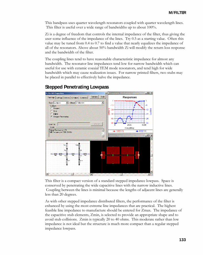
M/FILTER
133
This bandpass uses quarter wavelength resonators coupled with quarter wavelength lines. This filter is useful over a wide range of bandwidths up to about 100%.
Zi is a degree of freedom that controls the internal impedance of the filter, thus giving the user some influence of the impedance of the lines. Try 0.5 as a starting value. Often this value may be tuned from 0.4 to 0.7 to find a value that nearly equalizes the impedance of all of the resonators. Above about 50% bandwidth Zi will modify the return loss response and the bandwidth of the filter.
The coupling lines tend to have reasonable characteristic impedance for almost any bandwidth. The resonator line impedances tend low for narrow bandwidth which can useful for use with ceramic coaxial TEM mode resonators, and tend high for wide bandwidth which may cause realization issues. For narrow printed filters, two stubs may be placed in parallel to effectively halve the impedance.
Stepped Penetrating Lowpass
This filter is a compact version of a standard stepped impedance lowpass. Space is conserved by penetrating the wide capacitive lines with the narrow inductive lines. Coupling between the lines is minimal because the lengths of adjacent lines are generally less than 20 degrees.
As with other stepped impedance distributed filters, the performance of the filter is enhanced by using the most extreme line impedances that are practical. The highest feasible line impedance to manufacture should be entered for Zmax. The impedance of the capacitive stub elements, Zmin, is selected to provide an appropriate shape and to avoid stub collisions. Zmin is typically 20 to 40 ohms. This moderate rather than low impedance is not ideal but the structure is much more compact than a regular stepped impedance lowpass.

Synthesis
134
The length of the lines connecting the inductive lines and the capacitive stubs is generally very short, perhaps about 1/2 the PWB thickness. Lengthening these lines introduces notches in the stopband that may improve rejection at specific frequencies but will degrade rejection at higher frequencies.
When converted to microstrip, you will receive a warning that the step models are out of range. While this stresses the accuracy of the circuit theory simulation, the extreme step ratio is good for final filter performance. The circuit theory predicted cutoff frequency of this filter may be slightly lower than the prototype filter. EMPOWER simulation is advised if first pass prototype success is required.
135
Chapter 8: OSCILLATOR
OSCILLATOR: Operation
Overview OSCILLATOR assists with the design of L-C, transmission line, cavity, SAW and crystal oscillators.
Documentation for the OSCILLATOR program is in two parts. This section describes program operation. The book Oscillator Design and Computer Simulation, 2nd edition, covers theory and many practical examples. Oscillator Design is written to provide an understanding of fundamental oscillator principles. This frees the user from the shackles of specific rules and dogma, especially since computer simulation makes testing new design ideas quick and easy. The electronic edition of the book is included with the purchase of OSCILLATOR. (Click on the link above.) Printed copies of the book are available from Noble Publishing (www.noblepub.com).
OSCILLATOR quickly and conveniently synthesizes a variety of oscillators. However, the real power in oscillator design is in the combined synthesis/simulation environment of GENESYS. You may use the GENESYS simulator to quickly evaluate the OSCILLATOR design, study the effects of component changes, customize the design to specific requirements and explore new and unique oscillator designs. Since a nonlinear model is used for the active device, the dc voltages are displayed on the schematic for each node of the circuit. The linear analysis automatically linearizes the device about the operating point. The use of a nonlinear device model also allows the start-up transient to be simulated in the time domain. This can be used to determine the time to reach steady state conditions and the amplitude of the output. It also verifies the frequency of oscillation.
OSCILLATOR is used to design a range of different types of oscillators, including:
• Cavity Bipolar
• Cavity Hybrid
• Coaxial Hybrid
• LC Bipolar
• LC Clapp
• LC Colpitts
• LC Hybrid
• LC Rhea Hybrid

Synthesis
136
• Saw Bipolar
• Saw Hybrid
• Saw MOS
• Tline UHF VCO with Transformer
• Tline UHF VCO
• Crystal Colpitts
• Crystal Hi Performance
• Crystal Multiplier
• Crystal Overtone
• Crystal Pierce
• Negative Conductance VCO
Oscillator Walkthrough In this example, a 25 to 75 MHz LC Colpitts JFET oscillator is designed.
Note: This example assumes that you are familiar with drawing schematics and entering parameters.
To create this Oscillator:
1. Create a new workspace by selecting “New” on the File menu.
2. Click the New Item button in the Workspace Window and select Add Oscillator in the Synthesis submenu, as shown below:
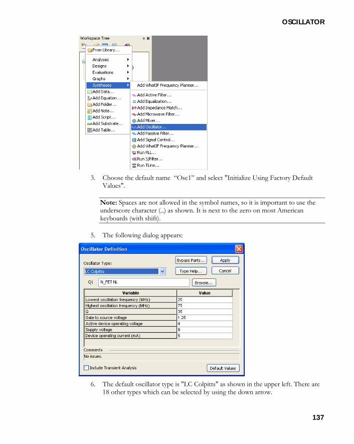
OSCILLATOR
137
3. Choose the default name “Osc1” and select "Initialize Using Factory Default
Values".
Note: Spaces are not allowed in the symbol names, so it is important to use the underscore character (_) as shown. It is next to the zero on most American keyboards (with shift).
5. The following dialog appears:
6. The default oscillator type is "LC Colpitts" as shown in the upper left. There are
18 other types which can be selected by using the down arrow.
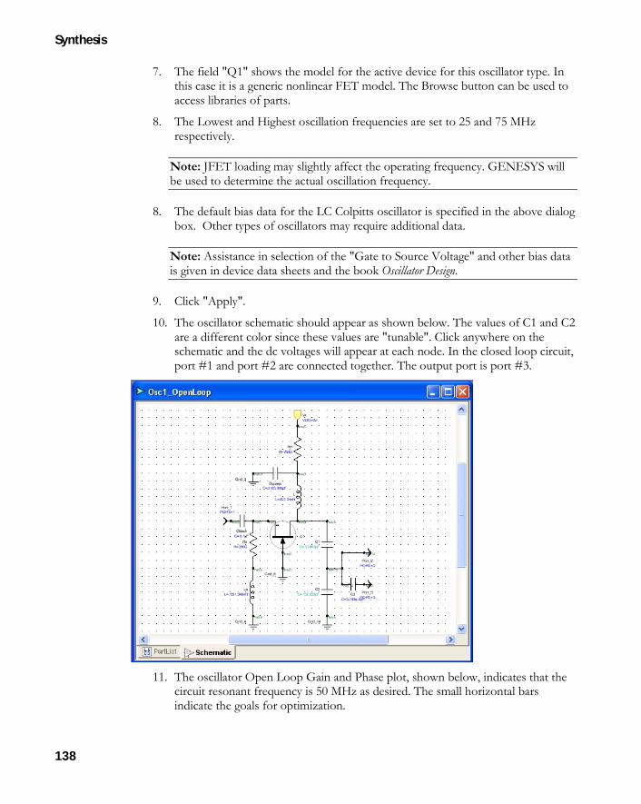
Synthesis
138
7. The field "Q1" shows the model for the active device for this oscillator type. In this case it is a generic nonlinear FET model. The Browse button can be used to access libraries of parts.
8. The Lowest and Highest oscillation frequencies are set to 25 and 75 MHz respectively.
Note: JFET loading may slightly affect the operating frequency. GENESYS will be used to determine the actual oscillation frequency.
8. The default bias data for the LC Colpitts oscillator is specified in the above dialog box. Other types of oscillators may require additional data.
Note: Assistance in selection of the "Gate to Source Voltage" and other bias data is given in device data sheets and the book Oscillator Design.
9. Click "Apply".
10. The oscillator schematic should appear as shown below. The values of C1 and C2 are a different color since these values are "tunable". Click anywhere on the schematic and the dc voltages will appear at each node. In the closed loop circuit, port #1 and port #2 are connected together. The output port is port #3.
11. The oscillator Open Loop Gain and Phase plot, shown below, indicates that the
circuit resonant frequency is 50 MHz as desired. The small horizontal bars indicate the goals for optimization.
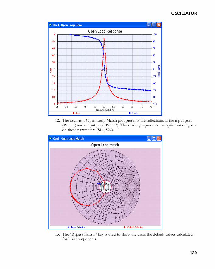
OSCILLATOR
139
12. The oscillator Open Loop Match plot presents the reflections at the input port
(Port_1) and output port (Port_2). The shading represents the optimization goals on these parameters (S11, S22).
13. The "Bypass Parts..." key is used to show the users the default values calculated
for bias components.

Synthesis
140
14. If the "Include Transient Analysis" box is checked, followed by pressing "Apply", a turn-on transient simulation with be executed. The resulting plot of the time history of the transient, the voltage at port #3, shows the buildup of the amplitude. Note that the peak-to-peak voltage in steady state is roughly 1 volt.
If the zoom is used, the frequency and waveform of a single cycle can be examined. As expected the period of the oscillation is 20ns for the design frequency of 50 MHz. Notice that the output is sinusoidal with few harmonics.
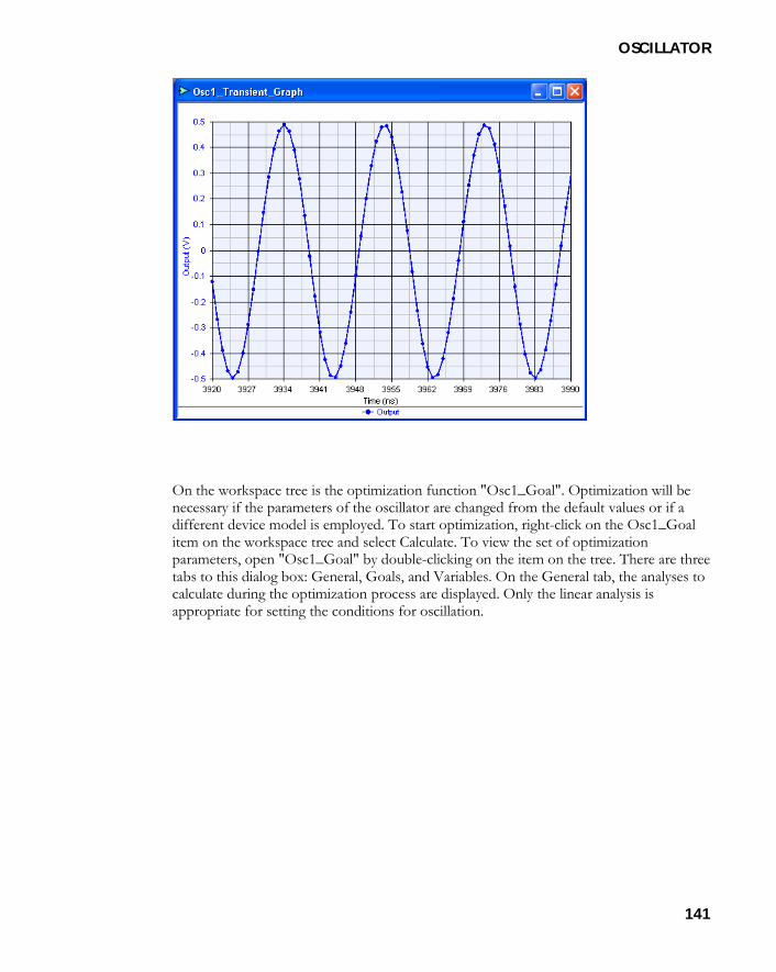
OSCILLATOR
141
On the workspace tree is the optimization function "Osc1_Goal". Optimization will be necessary if the parameters of the oscillator are changed from the default values or if a different device model is employed. To start optimization, right-click on the Osc1_Goal item on the workspace tree and select Calculate. To view the set of optimization parameters, open "Osc1_Goal" by double-clicking on the item on the tree. There are three tabs to this dialog box: General, Goals, and Variables. On the General tab, the analyses to calculate during the optimization process are displayed. Only the linear analysis is appropriate for setting the conditions for oscillation.

Synthesis
142
On the Goals tab, the targets for each measurement are set, as well as a weighting and the frequency range of interest. Notice that the range is a small frequency band around the design frequency, in this case 50 MHz. The phase is weighted more heavily since this determines the frequency of the oscillation.
The third tab defines the "tuned" variables or those to be optimized. The variables will not be shown until the "Get Tuned Variables" button is pressed. Limits (Min, Max) can be imposed on each variable to be "tuned". Since these fields are blank, there are no constraints on these variables.
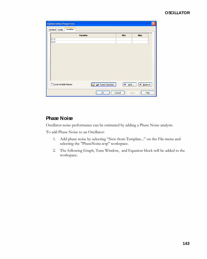
OSCILLATOR
143
Phase Noise Oscillator noise performance can be estimated by adding a Phase Noise analysis.
To add Phase Noise to an Oscillator:
1. Add phase noise by selecting “New from Template...” on the File menu and selecting the "PhaseNoise.wsp" workspace.
2. The following Graph, Tune Window, and Equation block will be added to the workspace.

Synthesis
144
3. Oscillator parameters can be changed in the tune window and the resulting phase
will be displayed in the graph.
FREQ_MHZ - This is the center frequency of the oscillator at which the phase noise is calculated and displayed. For broadband oscillators, the highest frequency may be entered to determine the worst-case noise.
QL - Oscillator loaded Q. The actual loaded Q may be determined by methods discussed in Oscillator Design.
FLICKER_HZ - Flicker noise corner frequency (hertz).
NF_DB - Noise figure of the active oscillator device.
BW_MHZ - This is the baseband frequency range (hertz) which is used to obtain the baseband residual FM and PM noise modulation.
OSCILLATOR
145
If a varactor is used to tune the oscillator, varactor modulation noise may contribute to the total oscillator phase noise. Varactor modulation noise increases with increased tuning sensitivity. A varactor which tunes a given frequency range with a smaller voltage change, other factors being constant, results in greater phase noise. Therefore, an oscillator with several switched low tuning rate ranges, may result in improved phase noise performance. The same effect is not achieved with a coarse and fine tuning varactor, although this is a common misconception.
VTUNE - Varactor voltage tuning range.
NUM_RANGES - Number of varactor tuning ranges.
FLOW_HZ - Lower frequency (hertz) of the varactor tuning range.
FHI_HZ - Higher frequency (hertz) of the varactor tuning range.
POWER_DBM - Power level in dBm of the oscillator.
HARMONIC - Harmonic of the oscillator used for oscillation.
4. Once the phase noise parameters have been entered the phase noise graph will display the calculated performance. The vertical axis displays values in dBm.
See the book Oscillator Design for additional information on Loaded Q, Noise Figure, Flicker Noise Corner Frequency, Varactor Tuning, Bias Schemes, and other oscillator topics.
Negative Resistance Oscillators The negative resistance model for oscillator analysis and design is discussed in the book, Oscillator Design and Computer Simulation. The linear reflection coefficient is often plotted on a rectangular grid with a vertical scale of 0 to 10. The desired negative resistance component of S11 would plot outside the circumference of a normal unity radius Smith chart. To overcome this difficulty, engineers using the negative resistance model to design oscillators sometimes plot 1/S11 on a Smith chart.
To plot 1/S11, simply add the variable S11_inv to the "Osc1_Linear Analysis" dataset. This is done by right-clicking in the variable area of the dataset dialog box and selecting "Add New Variable". Use a name such as S11_inv. In the formula field add: 1/S[1,1]. Then in the Graph Properties box for the Smith chart, replace S11 with S11_inv.
As explained in Oscillator Design, oscillation occurs at the frequency where the phase of S11 is either zero or 180° (S11 is non-reactive). The transition from zero to 180° is simply an indication that the negative resistance is greater than or less than the normalized plotting impedance. You may explore this by tuning the capacitor and observing S11 on the rectangular and Smith plots.
Component Defaults Component unloaded Q reduces the loop gain margin when the oscillator is designed with a loaded Q which approaches the component unloaded Q. OSCILLATOR computes component values based on its assumption of reasonable loaded Q for each oscillator
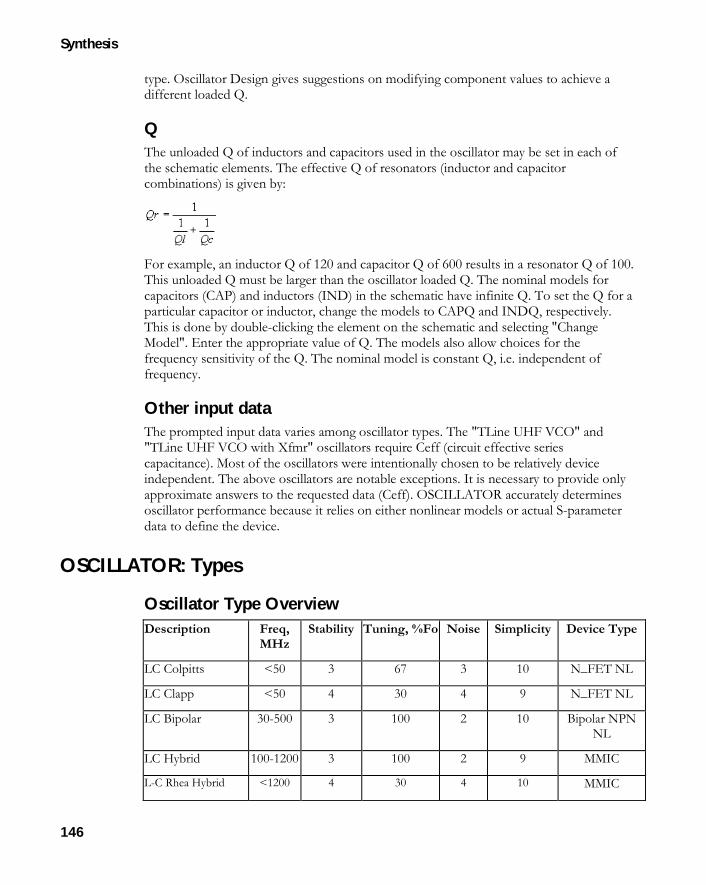
Synthesis
146
type. Oscillator Design gives suggestions on modifying component values to achieve a different loaded Q.
Q The unloaded Q of inductors and capacitors used in the oscillator may be set in each of the schematic elements. The effective Q of resonators (inductor and capacitor combinations) is given by:
For example, an inductor Q of 120 and capacitor Q of 600 results in a resonator Q of 100. This unloaded Q must be larger than the oscillator loaded Q. The nominal models for capacitors (CAP) and inductors (IND) in the schematic have infinite Q. To set the Q for a particular capacitor or inductor, change the models to CAPQ and INDQ, respectively. This is done by double-clicking the element on the schematic and selecting "Change Model". Enter the appropriate value of Q. The models also allow choices for the frequency sensitivity of the Q. The nominal model is constant Q, i.e. independent of frequency.
Other input data The prompted input data varies among oscillator types. The "TLine UHF VCO" and "TLine UHF VCO with Xfmr" oscillators require Ceff (circuit effective series capacitance). Most of the oscillators were intentionally chosen to be relatively device independent. The above oscillators are notable exceptions. It is necessary to provide only approximate answers to the requested data (Ceff). OSCILLATOR accurately determines oscillator performance because it relies on either nonlinear models or actual S-parameter data to define the device.
OSCILLATOR: Types
Oscillator Type Overview Description Freq,
MHz Stability Tuning, %Fo Noise Simplicity Device Type
LC Colpitts <50 3 67 3 10 N_FET NL
LC Clapp <50 4 30 4 9 N_FET NL
LC Bipolar 30-500 3 100 2 10 Bipolar NPN NL
LC Hybrid 100-1200 3 100 2 9 MMIC
L-C Rhea Hybrid <1200 4 30 4 10 MMIC

OSCILLATOR
147
UHF VCO 300-2000 1 67 1 10 Bipolar NPN NL
VCO w/XFRM 200-1200 2 100 2 9 Bipolar NPN NL
Cavity Bipolar 300-2000 4 67 5 1 Bipolar NPN NL
Cavity Hybrid 300-2000 4 67 5 1 MMIC
Coax Hybrid 300-2000 4 10 5 6 MMIC
Neg-G VCO <2000 2 100 3 5 Bipolar NPN NL
SAW 180 1-port 200-1000 5 .02 6 3 Bipolar NPN NL
SAW Hybrid 2-p 200-1200 5 .05 6 3 MMIC
SAW MOSFET 2-p 200-1000 5 .03 6 3 MOS_2_Gate
XTAL Pierce 1-20 8 .2 8 6 Bipolar NPN NL
XTAL Colpitts 4-20 6 NIL 6 6 Bipolar NPN NL
XTAL High Perform.
1-20 9 .2 9 5 Bipolar NPN NL
XTAL Overtone 20-200 7 NIL 7 6 Bipolar NPN NL
XTAL Over+Mult 50-600 7 .2 7 6 Bipolar NPN NL
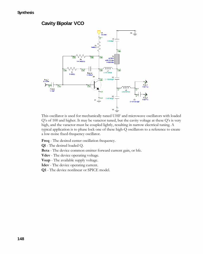
Synthesis
148
Cavity Bipolar VCO
This oscillator is used for mechanically tuned UHF and microwave oscillators with loaded Q’s of 100 and higher. It may be varactor tuned, but the cavity voltage at these Q’s is very high, and the varactor must be coupled lightly, resulting in narrow electrical tuning. A typical application is to phase lock one of these high-Q oscillators to a reference to create a low-noise fixed-frequency oscillator.
Freq - The desired center oscillation frequency. Ql - The desired loaded Q. Beta - The device common emitter forward current gain, or hfe. Vdev - The device operating voltage. Vsup - The available supply voltage. Idev - The device operating current. Q1 - The device nonlinear or SPICE model.

OSCILLATOR
149
Cavity Hybrid VCO
This is simply a hybrid version of the Cavity Bipolar oscillator. This oscillator is used for mechanically tuned UHF and microwave oscillators with loaded Q’s of 100 and higher. It may be varactor tuned, but the cavity voltage at these Q’s is very high, and the varactor must be coupled lightly, resulting in narrow electrical tuning. A typical application is to phase lock one of these high-Q oscillators to a reference to create a low-noise fixed-frequency oscillator.
Freq - The desired oscillation frequency. Ql - The desired loaded Q. Vdev - The device operating voltage. Idev - The device operating current. Q1 - The device nonlinear or SPICE model.
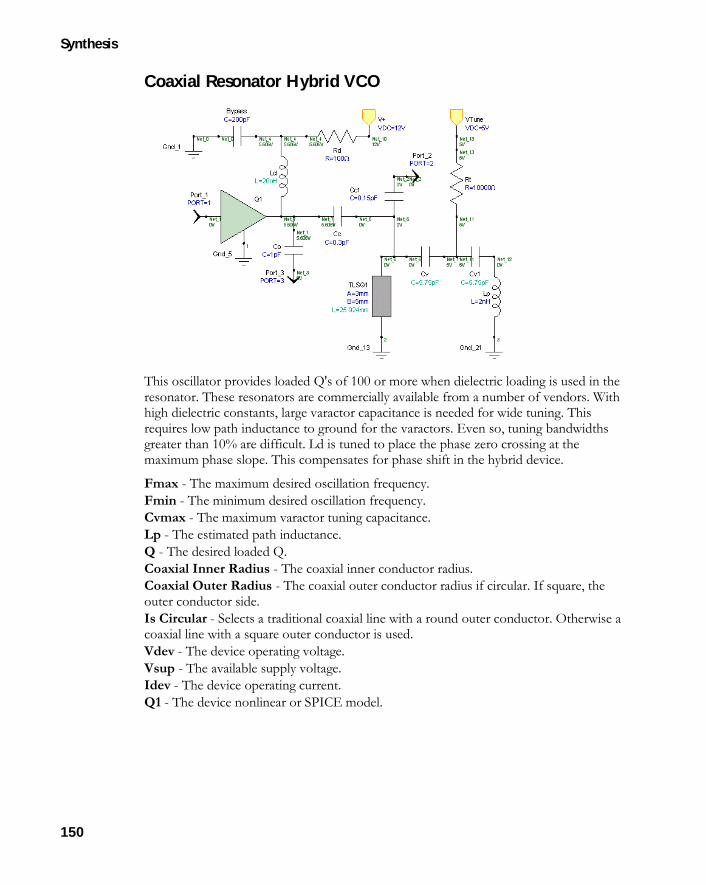
Synthesis
150
Coaxial Resonator Hybrid VCO
This oscillator provides loaded Q's of 100 or more when dielectric loading is used in the resonator. These resonators are commercially available from a number of vendors. With high dielectric constants, large varactor capacitance is needed for wide tuning. This requires low path inductance to ground for the varactors. Even so, tuning bandwidths greater than 10% are difficult. Ld is tuned to place the phase zero crossing at the maximum phase slope. This compensates for phase shift in the hybrid device.
Fmax - The maximum desired oscillation frequency. Fmin - The minimum desired oscillation frequency. Cvmax - The maximum varactor tuning capacitance. Lp - The estimated path inductance. Q - The desired loaded Q. Coaxial Inner Radius - The coaxial inner conductor radius. Coaxial Outer Radius - The coaxial outer conductor radius if circular. If square, the outer conductor side. Is Circular - Selects a traditional coaxial line with a round outer conductor. Otherwise a coaxial line with a square outer conductor is used. Vdev - The device operating voltage. Vsup - The available supply voltage. Idev - The device operating current. Q1 - The device nonlinear or SPICE model.
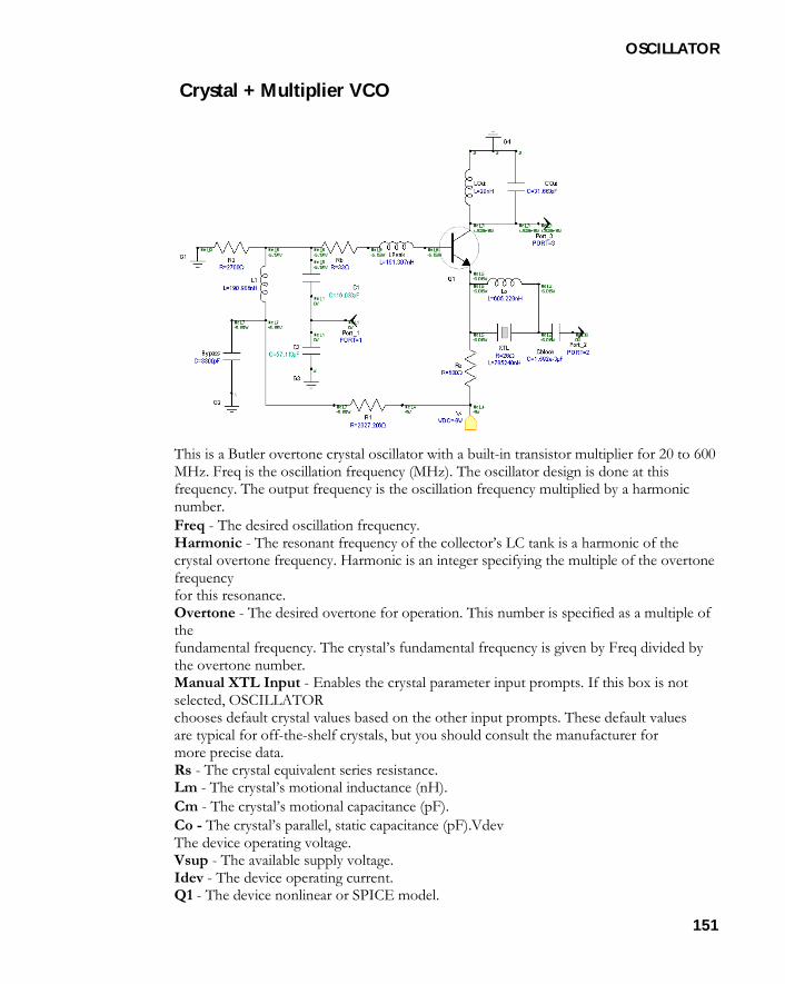
OSCILLATOR
151
Crystal + Multiplier VCO
This is a Butler overtone crystal oscillator with a built-in transistor multiplier for 20 to 600 MHz. Freq is the oscillation frequency (MHz). The oscillator design is done at this frequency. The output frequency is the oscillation frequency multiplied by a harmonic number. Freq - The desired oscillation frequency. Harmonic - The resonant frequency of the collector’s LC tank is a harmonic of the crystal overtone frequency. Harmonic is an integer specifying the multiple of the overtone frequency for this resonance. Overtone - The desired overtone for operation. This number is specified as a multiple of the fundamental frequency. The crystal’s fundamental frequency is given by Freq divided by the overtone number. Manual XTL Input - Enables the crystal parameter input prompts. If this box is not selected, OSCILLATOR chooses default crystal values based on the other input prompts. These default values are typical for off-the-shelf crystals, but you should consult the manufacturer for more precise data. Rs - The crystal equivalent series resistance. Lm - The crystal’s motional inductance (nH). Cm - The crystal’s motional capacitance (pF). Co - The crystal’s parallel, static capacitance (pF).Vdev The device operating voltage. Vsup - The available supply voltage. Idev - The device operating current. Q1 - The device nonlinear or SPICE model.
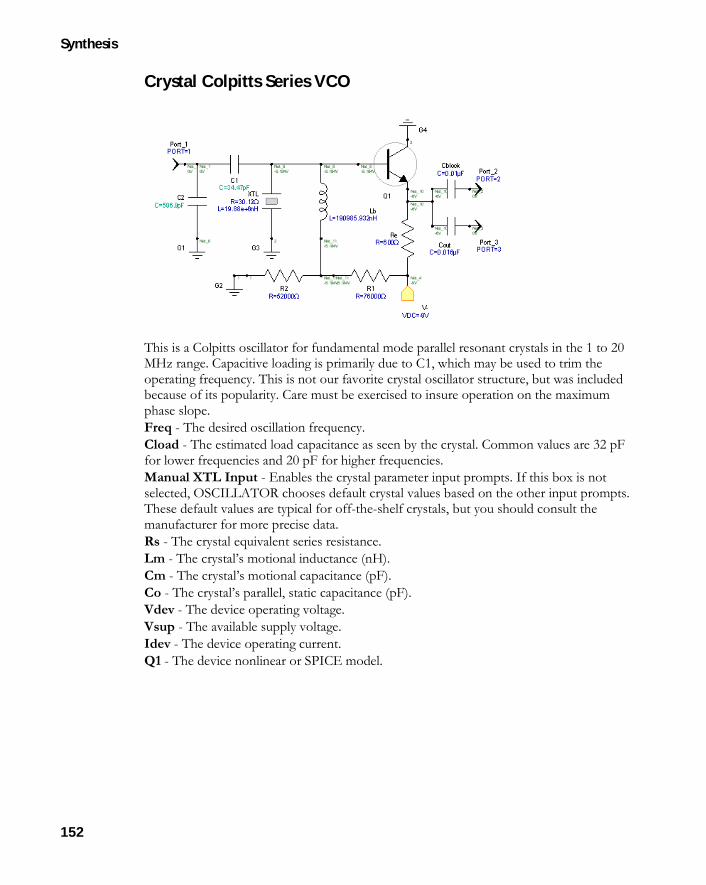
Synthesis
152
Crystal Colpitts Series VCO
This is a Colpitts oscillator for fundamental mode parallel resonant crystals in the 1 to 20 MHz range. Capacitive loading is primarily due to C1, which may be used to trim the operating frequency. This is not our favorite crystal oscillator structure, but was included because of its popularity. Care must be exercised to insure operation on the maximum phase slope. Freq - The desired oscillation frequency. Cload - The estimated load capacitance as seen by the crystal. Common values are 32 pF for lower frequencies and 20 pF for higher frequencies. Manual XTL Input - Enables the crystal parameter input prompts. If this box is not selected, OSCILLATOR chooses default crystal values based on the other input prompts. These default values are typical for off-the-shelf crystals, but you should consult the manufacturer for more precise data. Rs - The crystal equivalent series resistance. Lm - The crystal’s motional inductance (nH). Cm - The crystal’s motional capacitance (pF). Co - The crystal’s parallel, static capacitance (pF). Vdev - The device operating voltage. Vsup - The available supply voltage. Idev - The device operating current. Q1 - The device nonlinear or SPICE model.
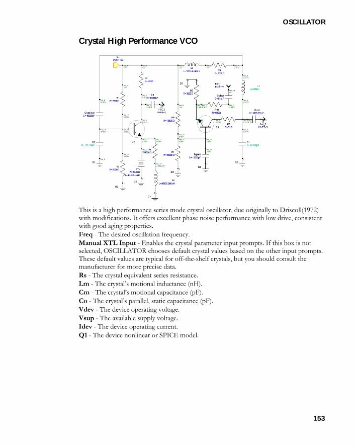
OSCILLATOR
153
Crystal High Performance VCO
This is a high performance series mode crystal oscillator, due originally to Driscoll(1972) with modifications. It offers excellent phase noise performance with low drive, consistent with good aging properties. Freq - The desired oscillation frequency. Manual XTL Input - Enables the crystal parameter input prompts. If this box is not selected, OSCILLATOR chooses default crystal values based on the other input prompts. These default values are typical for off-the-shelf crystals, but you should consult the manufacturer for more precise data. Rs - The crystal equivalent series resistance. Lm - The crystal’s motional inductance (nH). Cm - The crystal’s motional capacitance (pF). Co - The crystal’s parallel, static capacitance (pF). Vdev - The device operating voltage. Vsup - The available supply voltage. Idev - The device operating current. Q1 - The device nonlinear or SPICE model.
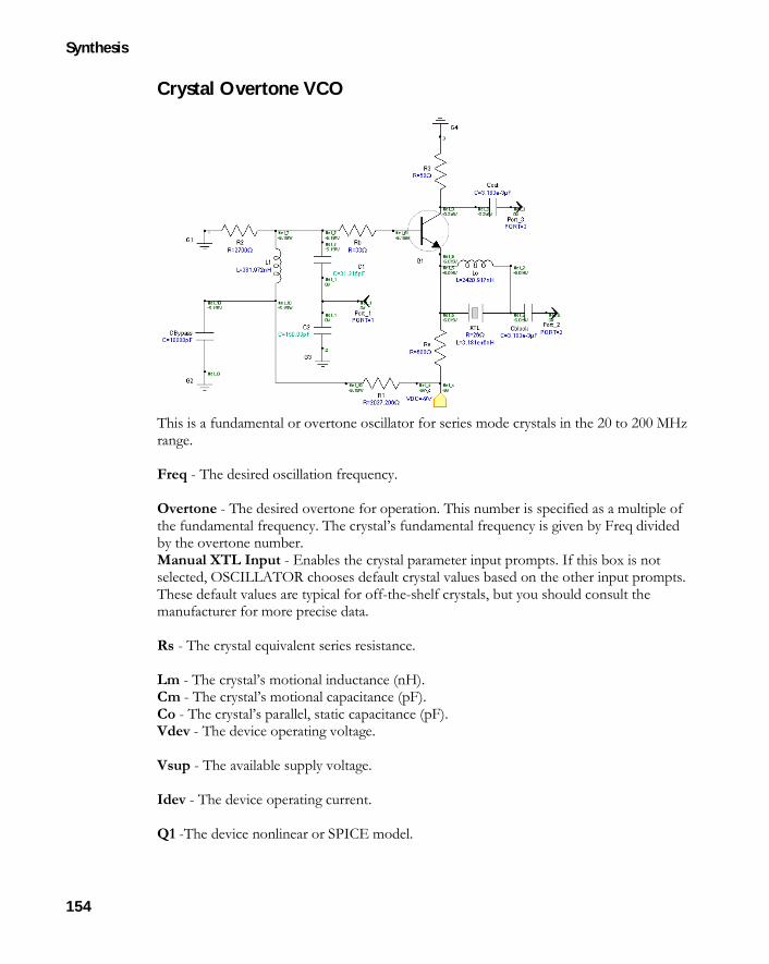
Synthesis
154
Crystal Overtone VCO
This is a fundamental or overtone oscillator for series mode crystals in the 20 to 200 MHz range. Freq - The desired oscillation frequency. Overtone - The desired overtone for operation. This number is specified as a multiple of the fundamental frequency. The crystal’s fundamental frequency is given by Freq divided by the overtone number. Manual XTL Input - Enables the crystal parameter input prompts. If this box is not selected, OSCILLATOR chooses default crystal values based on the other input prompts. These default values are typical for off-the-shelf crystals, but you should consult the manufacturer for more precise data. Rs - The crystal equivalent series resistance. Lm - The crystal’s motional inductance (nH). Cm - The crystal’s motional capacitance (pF). Co - The crystal’s parallel, static capacitance (pF). Vdev - The device operating voltage. Vsup - The available supply voltage. Idev - The device operating current. Q1 -The device nonlinear or SPICE model.
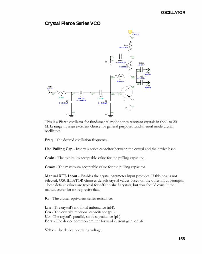
OSCILLATOR
155
Crystal Pierce Series VCO
This is a Pierce oscillator for fundamental mode series resonant crystals in the.1 to 20 MHz range. It is an excellent choice for general purpose, fundamental mode crystal oscillators. Freq - The desired oscillation frequency. Use Pulling Cap - Inserts a series capacitor between the crystal and the device base. Cmin - The minimum acceptable value for the pulling capacitor. Cmax - The maximum acceptable value for the pulling capacitor. Manual XTL Input - Enables the crystal parameter input prompts. If this box is not selected, OSCILLATOR chooses default crystal values based on the other input prompts. These default values are typical for off-the-shelf crystals, but you should consult the manufacturer for more precise data. Rs - The crystal equivalent series resistance. Lm - The crystal’s motional inductance (nH). Cm - The crystal’s motional capacitance (pF). Co - The crystal’s parallel, static capacitance (pF). Beta - The device common emitter forward current gain, or hfe. Vdev - The device operating voltage.
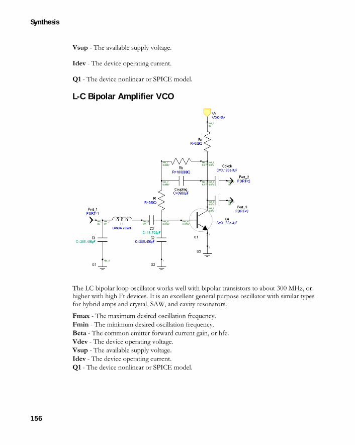
Synthesis
156
Vsup - The available supply voltage. Idev - The device operating current. Q1 - The device nonlinear or SPICE model.
L-C Bipolar Amplifier VCO
The LC bipolar loop oscillator works well with bipolar transistors to about 300 MHz, or higher with high Ft devices. It is an excellent general purpose oscillator with similar types for hybrid amps and crystal, SAW, and cavity resonators.
Fmax - The maximum desired oscillation frequency. Fmin - The minimum desired oscillation frequency. Beta - The common emitter forward current gain, or hfe. Vdev - The device operating voltage. Vsup - The available supply voltage. Idev - The device operating current. Q1 - The device nonlinear or SPICE model.
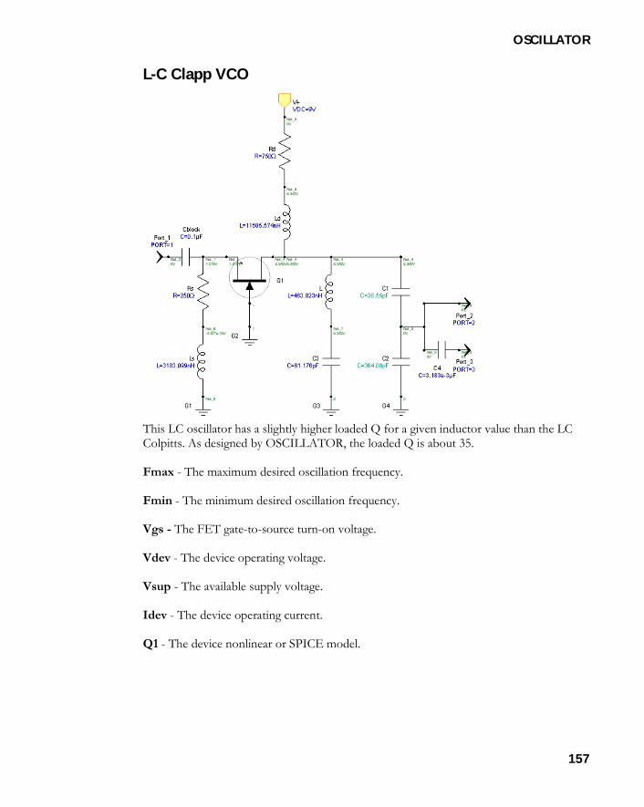
OSCILLATOR
157
L-C Clapp VCO
This LC oscillator has a slightly higher loaded Q for a given inductor value than the LC Colpitts. As designed by OSCILLATOR, the loaded Q is about 35. Fmax - The maximum desired oscillation frequency. Fmin - The minimum desired oscillation frequency. Vgs - The FET gate-to-source turn-on voltage. Vdev - The device operating voltage. Vsup - The available supply voltage. Idev - The device operating current. Q1 - The device nonlinear or SPICE model.

Synthesis
158
L-C Colpitts VCO
This LC oscillator is of the common base configuration. As designed by OSCILLATOR, the loaded Q is about 35. Fmax - The maximum desired oscillation frequency. Fmin - The minimum desired oscillation frequency. Vgs - The FET gate-to-source turn-on voltage. Vdev - The device operating voltage. Vsup - The available supply voltage. Idev - The device operating current. Q1 - The device nonlinear or SPICE model.
L-C Hybrid Amplifier VCO
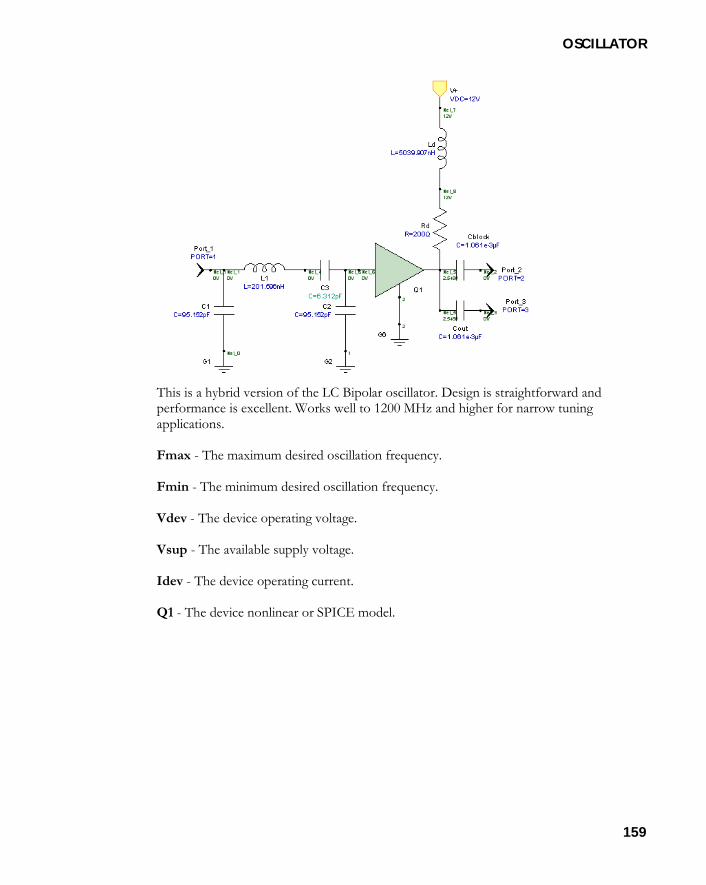
OSCILLATOR
159
This is a hybrid version of the LC Bipolar oscillator. Design is straightforward and performance is excellent. Works well to 1200 MHz and higher for narrow tuning applications. Fmax - The maximum desired oscillation frequency. Fmin - The minimum desired oscillation frequency. Vdev - The device operating voltage. Vsup - The available supply voltage. Idev - The device operating current. Q1 - The device nonlinear or SPICE model.

Synthesis
160
L-C Rhea Hybrid VCO
This oscillator offers economy, very fast starting and excellent harmonic performance. The amplifier should be inverting such as the MSA series of MMICs. As with all oscillators the small-signal open loop gain should be moderate, perhaps 3 to 8 dB. If the phase zero crossing occurs at a much lower frequency than the maximum phase slope, the supply resistor may be replaced with an inductor that is tuned until better alignment occurs. If a supply resistor is required it should then be bypassed. The selected value of C3 provides moderate output coupling. For reduced load pulling C3 may be increased. For increased output power, C3 may be decreased. REFERENCES THIS OSCILLATOR: Randall Rhea and Bill Clausen, Recent Trends in Oscillator Design, Microwave Journal, January 2004. OSCILLATOR DESIGN TECHNIQUES: Randall Rhea, Oscillator Design and Computer Simulation, Noble Publishing, Atlanta.
Freq - The desired center oscillation frequency. Vdev - The device operating voltage. Vsup - The available supply voltage. Idev - The device operating current. Q1 - The device nonlinear or SPICE model. Example
Freq = 100 MHz, Vdev = 5, Vsup = 9.6, Idev = 35 ma
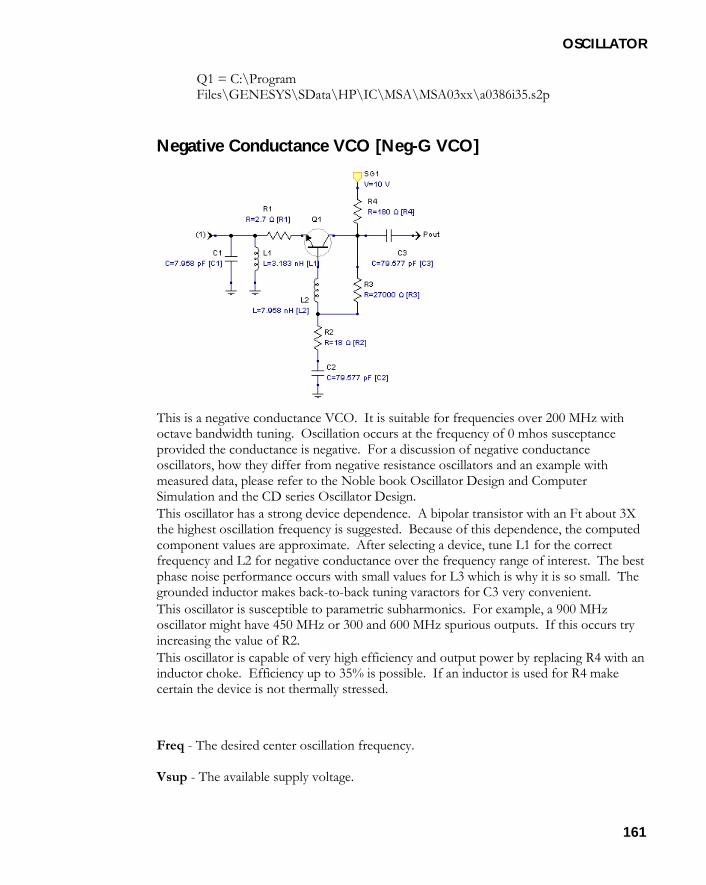
OSCILLATOR
161
Q1 = C:\Program Files\GENESYS\SData\HP\IC\MSA\MSA03xx\a0386i35.s2p
Negative Conductance VCO [Neg-G VCO]
This is a negative conductance VCO. It is suitable for frequencies over 200 MHz with octave bandwidth tuning. Oscillation occurs at the frequency of 0 mhos susceptance provided the conductance is negative. For a discussion of negative conductance oscillators, how they differ from negative resistance oscillators and an example with measured data, please refer to the Noble book Oscillator Design and Computer Simulation and the CD series Oscillator Design. This oscillator has a strong device dependence. A bipolar transistor with an Ft about 3X the highest oscillation frequency is suggested. Because of this dependence, the computed component values are approximate. After selecting a device, tune L1 for the correct frequency and L2 for negative conductance over the frequency range of interest. The best phase noise performance occurs with small values for L3 which is why it is so small. The grounded inductor makes back-to-back tuning varactors for C3 very convenient. This oscillator is susceptible to parametric subharmonics. For example, a 900 MHz oscillator might have 450 MHz or 300 and 600 MHz spurious outputs. If this occurs try increasing the value of R2. This oscillator is capable of very high efficiency and output power by replacing R4 with an inductor choke. Efficiency up to 35% is possible. If an inductor is used for R4 make certain the device is not thermally stressed.
Freq - The desired center oscillation frequency. Vsup - The available supply voltage.
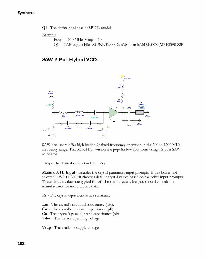
Synthesis
162
Q1 - The device nonlinear or SPICE model.
Example Freq = 1000 MHz, Vsup = 10 Q1 = C:\Program Files\GENESYS\SData\Motorola\MRF5XX\MRF559B.S2P
SAW 2 Port Hybrid VCO
SAW oscillators offer high loaded-Q fixed frequency operation in the 200 to 1200 MHz frequency range. This MOSFET version is a popular low cost form using a 2-port SAW resonator. Freq - The desired oscillation frequency. Manual XTL Input - Enables the crystal parameter input prompts. If this box is not selected, OSCILLATOR chooses default crystal values based on the other input prompts. These default values are typical for off-the-shelf crystals, but you should consult the manufacturer for more precise data. Rs - The crystal equivalent series resistance. Lm - The crystal’s motional inductance (nH). Cm - The crystal’s motional capacitance (pF). Co - The crystal’s parallel, static capacitance (pF). Vdev - The device operating voltage. Vsup - The available supply voltage.

OSCILLATOR
163
Idev - The device operating current. Q1 - The device nonlinear or SPICE model.
SAW 2 Port MOS VCO
SAW oscillators offer high loaded-Q fixed frequency operation in the 200 to 1200 MHz frequency range. This oscillator offers the best potential for performance and pulling of the SAW forms. Freq - The desired oscillation center frequency. Manual XTL Input - Enables the crystal parameter input prompts. If this box is not selected, OSCILLATOR chooses default crystal values based on the other input prompts. These default values are typical for off-the-shelf crystals, but you should consult the manufacturer for more precise data. Rs - The crystal equivalent series resistance. Lm - The crystal’s motional inductance (nH). Cm - The crystal’s motional capacitance (pF). Co - The crystal’s parallel, static capacitance (pF). Vg1s - The gate 1 to source voltage. Vg2s - The gate 2 to source voltage. Vdev - The device operating voltage. Vsup - The available supply voltage.
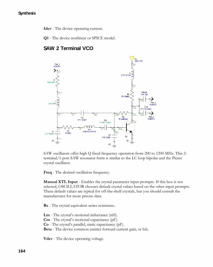
Synthesis
164
Idev - The device operating current. Q1 - The device nonlinear or SPICE model.
SAW 2 Terminal VCO
SAW oscillators offer high Q fixed frequency operation from 200 to 1200 MHz. This 2-terminal/1-port SAW resonator form is similar to the LC loop bipolar and the Pierce crystal oscillator. Freq - The desired oscillation frequency. Manual XTL Input - Enables the crystal parameter input prompts. If this box is not selected, OSCILLATOR chooses default crystal values based on the other input prompts. These default values are typical for off-the-shelf crystals, but you should consult the manufacturer for more precise data. Rs - The crystal equivalent series resistance. Lm - The crystal’s motional inductance (nH). Cm - The crystal’s motional capacitance (pF). Co - The crystal’s parallel, static capacitance (pF). Beta - The device common emitter forward current gain, or hfe. Vdev - The device operating voltage.
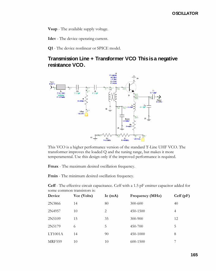
OSCILLATOR
165
Vsup - The available supply voltage. Idev - The device operating current. Q1 - The device nonlinear or SPICE model.
Transmission Line + Transformer VCO This is a negative resistance VCO.
This VCO is a higher performance version of the standard T-Line UHF VCO. The transformer improves the loaded Q and the tuning range, but makes it more temperamental. Use this design only if the improved performance is required. Fmax - The maximum desired oscillation frequency. Fmin - The minimum desired oscillation frequency. Ceff - The effective circuit capacitance. Ceff with a 1.5 pF emitter capacitor added for some common transistors is: Device Vce (Volts) Ie (mA) Frequency (MHz) Ceff (pF)
2N3866 14 80 300-600 40
2N4957 10 2 450-1500 4
2N5109 15 35 300-900 12
2N5179 6 5 450-700 5
LT1001A 14 90 450-1000 8
MRF559 10 10 600-1500 7
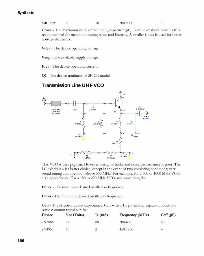
Synthesis
166
MRF559 10 50 300-2000 7
Cmax - The maximum value of the tuning capacitor (pF). A value of about twice Ceff is recommended for maximum tuning range and linearity. A smaller Cmax is used for better noise performance. Vdev - The device operating voltage. Vsup - The available supply voltage. Idev - The device operating current. Q1 - The device nonlinear or SPICE model.
Transmission Line UHF VCO
This VCO is very popular. However, design is tricky and noise performance is poor. The LC hybrid is a far better choice, except in the event of two coexisting conditions; very broad tuning and operation above 300 MHz. For example, for a 500 to 1000 MHz VCO, it's a good choice. For a 180 to 220 MHz VCO, use something else. Fmax - The maximum desired oscillation frequency. Fmin - The minimum desired oscillation frequency. Ceff - The effective circuit capacitance. Ceff with a 1.5 pF emitter capacitor added for some common transistors is: Device Vce (Volts) Ie (mA) Frequency (MHz) Ceff (pF)
2N3866 14 80 300-600 40
2N4957 10 2 450-1500 4
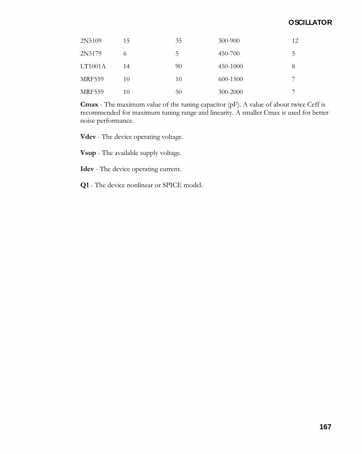
OSCILLATOR
167
2N5109 15 35 300-900 12
2N5179 6 5 450-700 5
LT1001A 14 90 450-1000 8
MRF559 10 10 600-1500 7
MRF559 10 50 300-2000 7
Cmax - The maximum value of the tuning capacitor (pF). A value of about twice Ceff is recommended for maximum tuning range and linearity. A smaller Cmax is used for better noise performance. Vdev - The device operating voltage. Vsup - The available supply voltage. Idev - The device operating current. Q1 - The device nonlinear or SPICE model.

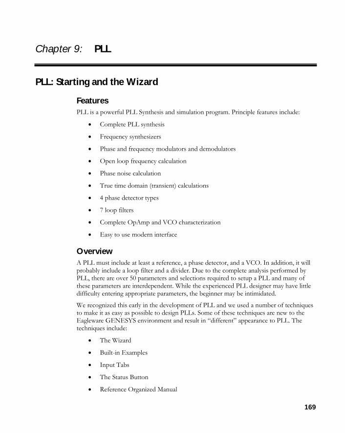
169
Chapter 9: PLL
PLL: Starting and the Wizard
Features PLL is a powerful PLL Synthesis and simulation program. Principle features include:
• Complete PLL synthesis
• Frequency synthesizers
• Phase and frequency modulators and demodulators
• Open loop frequency calculation
• Phase noise calculation
• True time domain (transient) calculations
• 4 phase detector types
• 7 loop filters
• Complete OpAmp and VCO characterization
• Easy to use modern interface
Overview A PLL must include at least a reference, a phase detector, and a VCO. In addition, it will probably include a loop filter and a divider. Due to the complete analysis performed by PLL, there are over 50 parameters and selections required to setup a PLL and many of these parameters are interdependent. While the experienced PLL designer may have little difficulty entering appropriate parameters, the beginner may be intimidated.
We recognized this early in the development of PLL and we used a number of techniques to make it as easy as possible to design PLLs. Some of these techniques are new to the Eagleware GENESYS environment and result in “different” appearance to PLL. The techniques include:
• The Wizard
• Built-in Examples
• Input Tabs
• The Status Button
• Reference Organized Manual

Synthesis
170
In the “reference organized manual,” most definitions, help and descriptions are given in a single section of the manual, organized by Menu item and Input Tab. This avoids searching throughout the manual for information on different subjects. It has the unusual effect of introducing some theory in the reference section, but we felt this would make the manual easier to use.
If you are new to PLLs you might want to read the section on Concepts, before beginning this section, which describes the Wizard and the built-in examples. Thereafter, you may need to refer only to the Reference section.
Status Button Another technique we created to simplify PLL design was the Status Button. The Status Button is located on the Status line at the bottom of the PLL screen. The Status Button has five color states: background, green, yellow, red and black. When the Status Button is any color except background, clicking on it opens a dialog box which contains one or messages. The messages provided in the first release of PLL are listed in the section on PLL Messages.
We suggest that you establish the habit of watching the Status Button and reading any messages, especially if the PLL is not operating as expected. The colored status categories are:
GREEN - These are informational messages. For example, selecting Override in the Filter Input Tab will light the Status Button green. This is done because you may later forget it was selected and changing other parameters might place the PLL in a non-functional state.
YELLOW - These are warning messages. For example, specifying a phase margin less than 30 degrees is risky because loop stability is marginal, particularly if the loop N must be variable or the there is tolerance in the values of loop components.
RED - These are messages which indicate a serious PLL problem. They will likely result in poor performance, total PLL failure or PLL simulation failure. For example, divider N times the reference frequency is not within the VCO frequency range.
BLACK - This condition should not occur. It indicates that PLL is in an error condition. Save your file and contact Eagleware.
Starting a New Design There are three recommended approaches to beginning a PLL design. If you are an experienced PLL designer, you may sequence through the Input Tabs — Simulation, Reference, Phase Detector/Divider, Loop Filter, VCO and Opamp — entering answers to each prompt.
Alternatively, you may select one of the examples from the Examples menu item and then change only those parameters which need to be changed. There is one example for each of the five PLL types plus an advanced example.
The most convenient method for both the beginner and the expert is to launch the Wizard from the Menu Bar and selecting a type of PLL. The Wizard provides online help
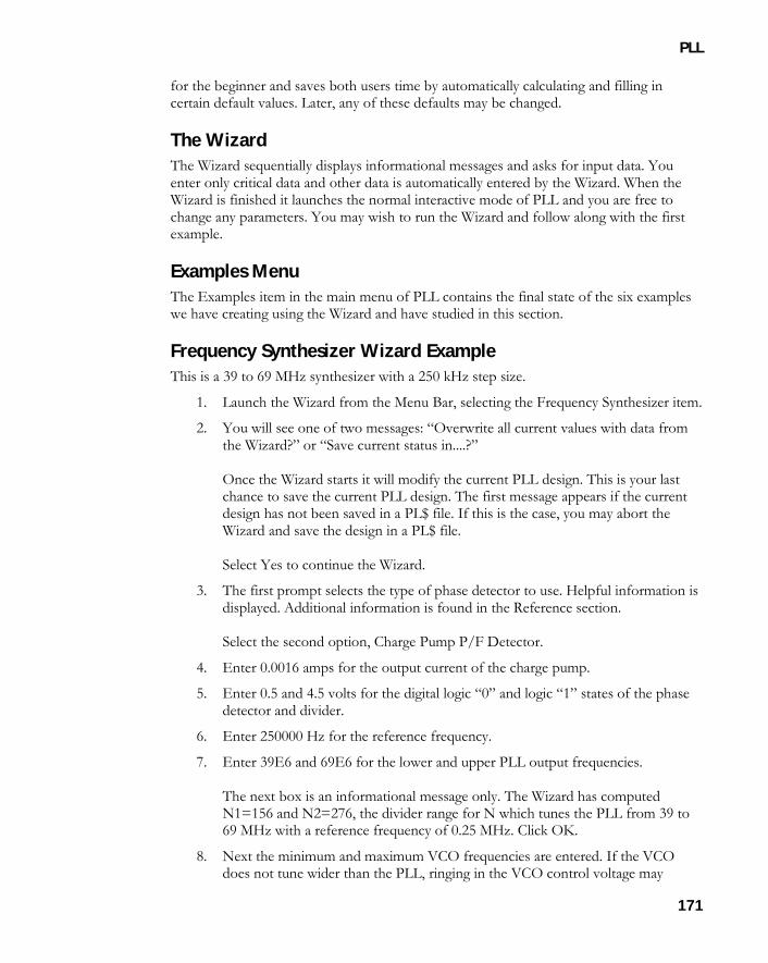
PLL
171
for the beginner and saves both users time by automatically calculating and filling in certain default values. Later, any of these defaults may be changed.
The Wizard The Wizard sequentially displays informational messages and asks for input data. You enter only critical data and other data is automatically entered by the Wizard. When the Wizard is finished it launches the normal interactive mode of PLL and you are free to change any parameters. You may wish to run the Wizard and follow along with the first example.
Examples Menu The Examples item in the main menu of PLL contains the final state of the six examples we have creating using the Wizard and have studied in this section.
Frequency Synthesizer Wizard Example This is a 39 to 69 MHz synthesizer with a 250 kHz step size.
1. Launch the Wizard from the Menu Bar, selecting the Frequency Synthesizer item.
2. You will see one of two messages: “Overwrite all current values with data from the Wizard?” or “Save current status in....?” Once the Wizard starts it will modify the current PLL design. This is your last chance to save the current PLL design. The first message appears if the current design has not been saved in a PL$ file. If this is the case, you may abort the Wizard and save the design in a PL$ file. Select Yes to continue the Wizard.
3. The first prompt selects the type of phase detector to use. Helpful information is displayed. Additional information is found in the Reference section. Select the second option, Charge Pump P/F Detector.
4. Enter 0.0016 amps for the output current of the charge pump.
5. Enter 0.5 and 4.5 volts for the digital logic “0” and logic “1” states of the phase detector and divider.
6. Enter 250000 Hz for the reference frequency.
7. Enter 39E6 and 69E6 for the lower and upper PLL output frequencies. The next box is an informational message only. The Wizard has computed N1=156 and N2=276, the divider range for N which tunes the PLL from 39 to 69 MHz with a reference frequency of 0.25 MHz. Click OK.
8. Next the minimum and maximum VCO frequencies are entered. If the VCO does not tune wider than the PLL, ringing in the VCO control voltage may

Synthesis
172
degrade or threaten lock behavior. The Wizard has selected minimum and maximum VCO frequencies with typically sufficient range to avoid lock problems. While safe for locking, in this case the default values represent well over an octave tuning bandwidth. Therefore, enter 35E6 and 73E6 for the VCO minimum and maximum frequencies.
9. Enter the VCO voltage at which the minimum frequency is achieved and the VCO voltage for the maximum VCO frequency. Select 0.5 volts for the minimum frequency and 4 volts for the maximum frequency.
10. Enter the loop bandwidth (the unity gain crossover frequency of the PLL open loop Bode response). We are interested in exceptionally good reference sideband rejection so a lower loop bandwidth is needed. Enter 2500 Hz which is 1/100 times the reference frequency.
11. Since excellent sideband rejection is needed select a 4th order filter. This is a passive loop filter. An opamp is not required because popular charge-pump phase detectors have a single-ended output.
12. PLL allows you to choose C1 in the loop filter. This value may be adjusted to effect other filter values. Inappropriate values may cause other filter values to be negative. These values may significantly effect loop locking and noise performance. Accept the default value of 1.2E-9 farads.
13. Again, to improve reference sideband rejection, we desire an extra loop filter.
14. Enter 5 for the order of the additional loop filter.
15. Enter 50000 Hz for the cutoff of the additional loop filter. Refer to the Ratios Table in the Concepts section for a discussion of the impact of an additional loop filter on stability.
16. Accept the default phase margin of 60 degrees.
17. The final dialog box provides information about other parameters selected for the VCO.
Wizard Synthesizer Results The Wizard has launched the normal interactive PLL mode. Click on the Frequency domain tab of the output window of PLL and select the Loop Resp radio button at the bottom of the output window. Select the open loop magnitude and angle traces (OL Mag and OL Ang) and turn off other responses by clicking on the check boxes to the left of the response description.
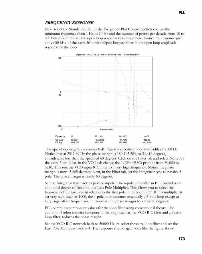
PLL
173
FREQUENCY RESPONSE Next select the Simulation tab. In the Frequency Plot Control section change the minimum frequency from 1 Hz to 10 Hz and the number of points per decade from 10 to 50. You should the see the open loop responses as shown here. Notice the response just above 50 kHz of the extra 5th order elliptic lowpass filter in the open loop amplitude response of the loop.
The open loop magnitude crosses 0 dB near the specified loop bandwidth of 2500 Hz. Notice that at 2511.89 Hz the phase margin is 180-145.584, or 34.416 degrees, considerably less than the specified 60 degrees. Click on the Filter tab and select None for the extra filter. Next, in the VCO tab change the 1/(2*pi*R*C) prompt from 50,000 to 5e10. This sets the VCO input R-C filter to a very high frequency. Notice the phase margin is now 45.869 degrees. Next, in the Filter tab, set the Integrator type to passive 3-pole. The phase margin is finally 60 degrees.
Set the Integrator type back to passive 4-pole. The 4-pole loop filter in PLL provides an additional degree of freedom, the Last Pole Multiplier. This allows you to select the frequency of the last pole in relation to the first pole in the loop filter. If this multiplier is set very high, such as 1000, the 4-pole loop becomes essentially a 3-pole loop except at very large offset frequencies. In this case, the phase margin becomes 60 degrees.
PLL computes component values for the loop filter using conventional theory. The addition of other transfer functions in the loop, such as the VCO R-C filter and an extra loop filter, reduces the phase margin.
Set the VCO R-C network back to 50000 Hz, re-select the extra loop filter and set the Last Pole Multiplier back at 4. The response should again look like the figure above.
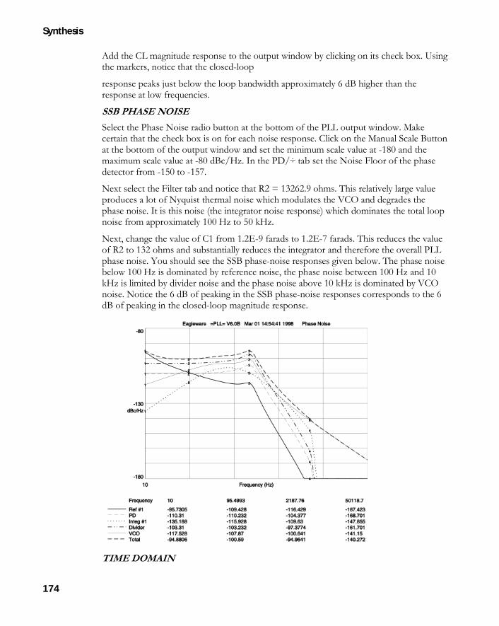
Synthesis
174
Add the CL magnitude response to the output window by clicking on its check box. Using the markers, notice that the closed-loop
response peaks just below the loop bandwidth approximately 6 dB higher than the response at low frequencies.
SSB PHASE NOISE Select the Phase Noise radio button at the bottom of the PLL output window. Make certain that the check box is on for each noise response. Click on the Manual Scale Button at the bottom of the output window and set the minimum scale value at -180 and the maximum scale value at -80 dBc/Hz. In the PD/÷ tab set the Noise Floor of the phase detector from -150 to -157.
Next select the Filter tab and notice that R2 = 13262.9 ohms. This relatively large value produces a lot of Nyquist thermal noise which modulates the VCO and degrades the phase noise. It is this noise (the integrator noise response) which dominates the total loop noise from approximately 100 Hz to 50 kHz.
Next, change the value of C1 from 1.2E-9 farads to 1.2E-7 farads. This reduces the value of R2 to 132 ohms and substantially reduces the integrator and therefore the overall PLL phase noise. You should see the SSB phase-noise responses given below. The phase noise below 100 Hz is dominated by reference noise, the phase noise between 100 Hz and 10 kHz is limited by divider noise and the phase noise above 10 kHz is dominated by VCO noise. Notice the 6 dB of peaking in the SSB phase-noise responses corresponds to the 6 dB of peaking in the closed-loop magnitude response.
TIME DOMAIN
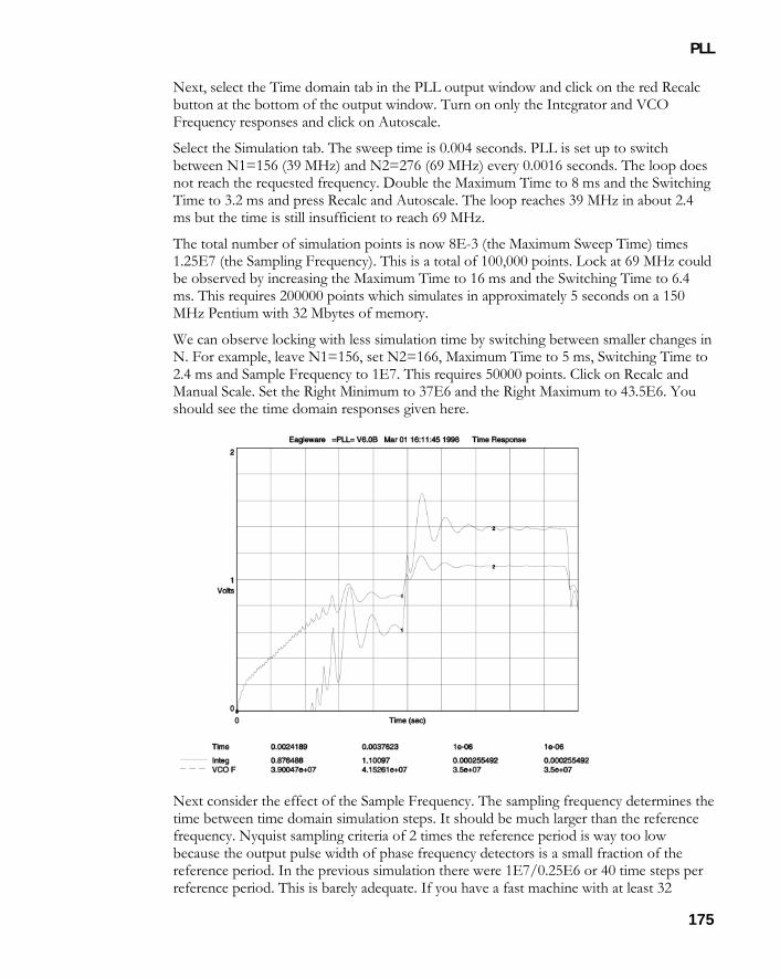
PLL
175
Next, select the Time domain tab in the PLL output window and click on the red Recalc button at the bottom of the output window. Turn on only the Integrator and VCO Frequency responses and click on Autoscale.
Select the Simulation tab. The sweep time is 0.004 seconds. PLL is set up to switch between N1=156 (39 MHz) and N2=276 (69 MHz) every 0.0016 seconds. The loop does not reach the requested frequency. Double the Maximum Time to 8 ms and the Switching Time to 3.2 ms and press Recalc and Autoscale. The loop reaches 39 MHz in about 2.4 ms but the time is still insufficient to reach 69 MHz.
The total number of simulation points is now 8E-3 (the Maximum Sweep Time) times 1.25E7 (the Sampling Frequency). This is a total of 100,000 points. Lock at 69 MHz could be observed by increasing the Maximum Time to 16 ms and the Switching Time to 6.4 ms. This requires 200000 points which simulates in approximately 5 seconds on a 150 MHz Pentium with 32 Mbytes of memory.
We can observe locking with less simulation time by switching between smaller changes in N. For example, leave N1=156, set N2=166, Maximum Time to 5 ms, Switching Time to 2.4 ms and Sample Frequency to 1E7. This requires 50000 points. Click on Recalc and Manual Scale. Set the Right Minimum to 37E6 and the Right Maximum to 43.5E6. You should see the time domain responses given here.
Next consider the effect of the Sample Frequency. The sampling frequency determines the time between time domain simulation steps. It should be much larger than the reference frequency. Nyquist sampling criteria of 2 times the reference period is way too low because the output pulse width of phase frequency detectors is a small fraction of the reference period. In the previous simulation there were 1E7/0.25E6 or 40 time steps per reference period. This is barely adequate. If you have a fast machine with at least 32
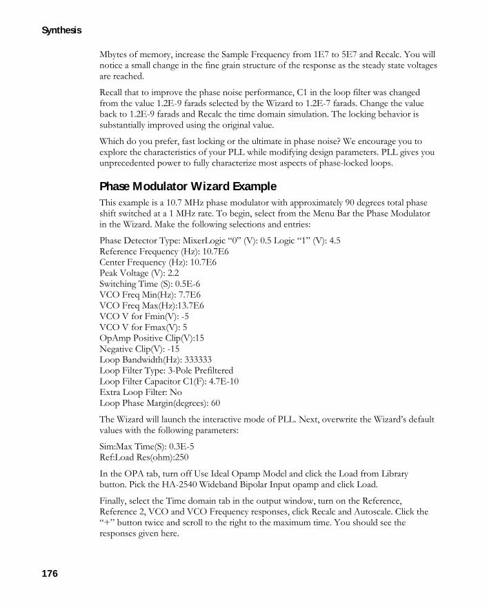
Synthesis
176
Mbytes of memory, increase the Sample Frequency from 1E7 to 5E7 and Recalc. You will notice a small change in the fine grain structure of the response as the steady state voltages are reached.
Recall that to improve the phase noise performance, C1 in the loop filter was changed from the value 1.2E-9 farads selected by the Wizard to 1.2E-7 farads. Change the value back to 1.2E-9 farads and Recalc the time domain simulation. The locking behavior is substantially improved using the original value.
Which do you prefer, fast locking or the ultimate in phase noise? We encourage you to explore the characteristics of your PLL while modifying design parameters. PLL gives you unprecedented power to fully characterize most aspects of phase-locked loops.
Phase Modulator Wizard Example This example is a 10.7 MHz phase modulator with approximately 90 degrees total phase shift switched at a 1 MHz rate. To begin, select from the Menu Bar the Phase Modulator in the Wizard. Make the following selections and entries:
Phase Detector Type: MixerLogic “0” (V): 0.5 Logic “1” (V): 4.5 Reference Frequency (Hz): 10.7E6 Center Frequency (Hz): 10.7E6 Peak Voltage (V): 2.2 Switching Time (S): 0.5E-6 VCO Freq Min(Hz): 7.7E6 VCO Freq Max(Hz):13.7E6 VCO V for Fmin(V): -5 VCO V for Fmax(V): 5 OpAmp Positive Clip(V):15 Negative Clip(V): -15 Loop Bandwidth(Hz): 333333 Loop Filter Type: 3-Pole Prefiltered Loop Filter Capacitor C1(F): 4.7E-10 Extra Loop Filter: No Loop Phase Margin(degrees): 60
The Wizard will launch the interactive mode of PLL. Next, overwrite the Wizard’s default values with the following parameters:
Sim:Max Time(S): 0.3E-5 Ref:Load Res(ohm):250
In the OPA tab, turn off Use Ideal Opamp Model and click the Load from Library button. Pick the HA-2540 Wideband Bipolar Input opamp and click Load.
Finally, select the Time domain tab in the output window, turn on the Reference, Reference 2, VCO and VCO Frequency responses, click Recalc and Autoscale. Click the “+” button twice and scroll to the right to the maximum time. You should see the responses given here.
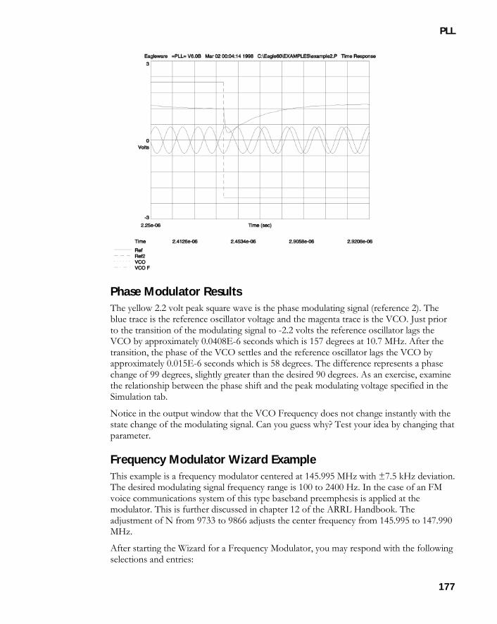
PLL
177
Phase Modulator Results The yellow 2.2 volt peak square wave is the phase modulating signal (reference 2). The blue trace is the reference oscillator voltage and the magenta trace is the VCO. Just prior to the transition of the modulating signal to -2.2 volts the reference oscillator lags the VCO by approximately 0.0408E-6 seconds which is 157 degrees at 10.7 MHz. After the transition, the phase of the VCO settles and the reference oscillator lags the VCO by approximately 0.015E-6 seconds which is 58 degrees. The difference represents a phase change of 99 degrees, slightly greater than the desired 90 degrees. As an exercise, examine the relationship between the phase shift and the peak modulating voltage specified in the Simulation tab.
Notice in the output window that the VCO Frequency does not change instantly with the state change of the modulating signal. Can you guess why? Test your idea by changing that parameter.
Frequency Modulator Wizard Example This example is a frequency modulator centered at 145.995 MHz with ±7.5 kHz deviation. The desired modulating signal frequency range is 100 to 2400 Hz. In the case of an FM voice communications system of this type baseband preemphesis is applied at the modulator. This is further discussed in chapter 12 of the ARRL Handbook. The adjustment of N from 9733 to 9866 adjusts the center frequency from 145.995 to 147.990 MHz.
After starting the Wizard for a Frequency Modulator, you may respond with the following selections and entries:
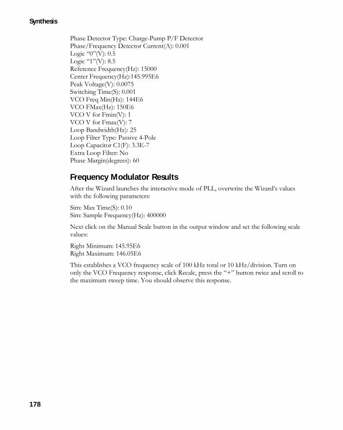
Synthesis
178
Phase Detector Type: Charge-Pump P/F Detector Phase/Frequency Detector Current(A): 0.001 Logic “0”(V): 0.5 Logic “1”(V): 8.5 Reference Frequency(Hz): 15000 Center Frequency(Hz):145.995E6 Peak Voltage(V): 0.0075 Switching Time(S): 0.001 VCO Freq Min(Hz): 144E6 VCO FMax(Hz): 150E6 VCO V for Fmin(V): 1 VCO V for Fmax(V): 7 Loop Bandwidth(Hz): 25 Loop Filter Type: Passive 4-Pole Loop Capacitor C1(F): 3.3E-7 Extra Loop Filter: No Phase Margin(degrees): 60
Frequency Modulator Results After the Wizard launches the interactive mode of PLL, overwrite the Wizard’s values with the following parameters:
Sim: Max Time(S): 0.10 Sim: Sample Frequency(Hz): 400000
Next click on the Manual Scale button in the output window and set the following scale values:
Right Minimum: 145.95E6 Right Maximum: 146.05E6
This establishes a VCO frequency scale of 100 kHz total or 10 kHz/division. Turn on only the VCO Frequency response, click Recalc, press the “+” button twice and scroll to the maximum sweep time. You should observe this response.
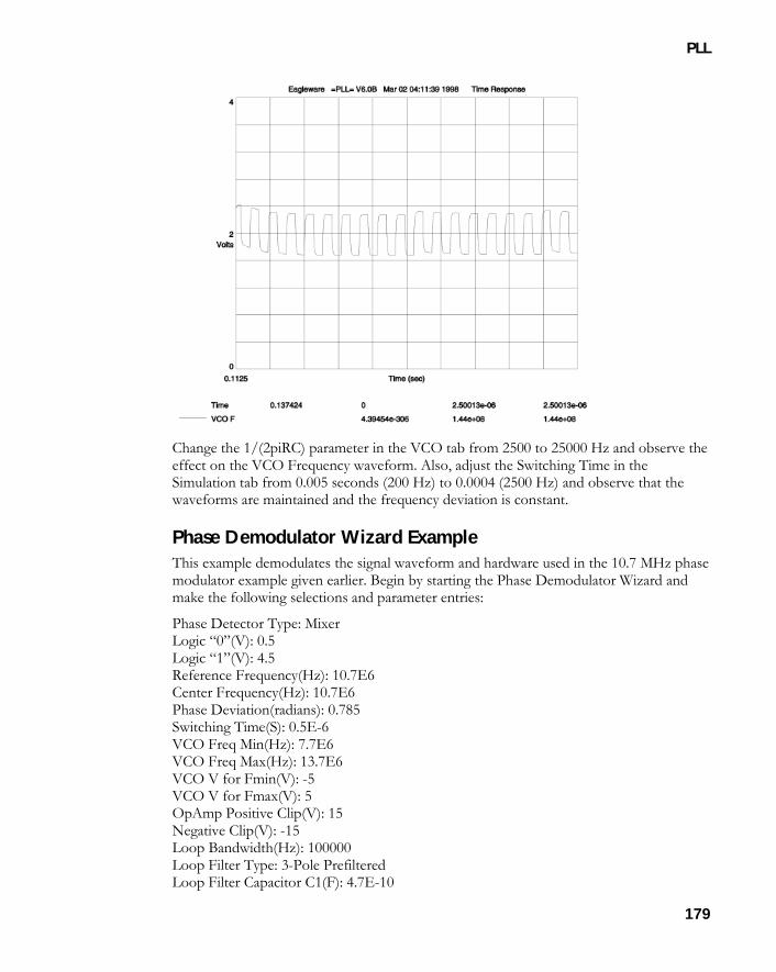
PLL
179
Change the 1/(2piRC) parameter in the VCO tab from 2500 to 25000 Hz and observe the effect on the VCO Frequency waveform. Also, adjust the Switching Time in the Simulation tab from 0.005 seconds (200 Hz) to 0.0004 (2500 Hz) and observe that the waveforms are maintained and the frequency deviation is constant.
Phase Demodulator Wizard Example This example demodulates the signal waveform and hardware used in the 10.7 MHz phase modulator example given earlier. Begin by starting the Phase Demodulator Wizard and make the following selections and parameter entries:
Phase Detector Type: Mixer Logic “0”(V): 0.5 Logic “1”(V): 4.5 Reference Frequency(Hz): 10.7E6 Center Frequency(Hz): 10.7E6 Phase Deviation(radians): 0.785 Switching Time(S): 0.5E-6 VCO Freq Min(Hz): 7.7E6 VCO Freq Max(Hz): 13.7E6 VCO V for Fmin(V): -5 VCO V for Fmax(V): 5 OpAmp Positive Clip(V): 15 Negative Clip(V): -15 Loop Bandwidth(Hz): 100000 Loop Filter Type: 3-Pole Prefiltered Loop Filter Capacitor C1(F): 4.7E-10
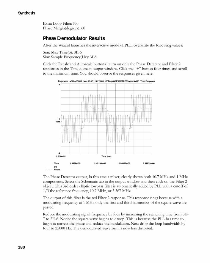
Synthesis
180
Extra Loop Filter: No Phase Margin(degrees): 60
Phase Demodulator Results After the Wizard launches the interactive mode of PLL, overwrite the following values:
Sim: Max Time(S): 3E-5 Sim: Sample Frequency(Hz): 3E8
Click the Recalc and Autoscale buttons. Turn on only the Phase Detector and Filter 2 responses in the Time domain output window. Click the “+” button four times and scroll to the maximum time. You should observe the responses given here.
The Phase Detector output, in this case a mixer, clearly shows both 10.7 MHz and 1 MHz components. Select the Schematic tab in the output window and then click on the Filter 2 object. This 3rd order elliptic lowpass filter is automatically added by PLL with a cutoff of 1/3 the reference frequency, 10.7 MHz, or 3.567 MHz.
The output of this filter is the red Filter 2 response. This response rings because with a modulating frequency at 1 MHz only the first and third harmonics of the square wave are passed.
Reduce the modulating signal frequency by four by increasing the switching time from 5E-7 to 2E-6. Notice the square wave begins to droop. This is because the PLL has time to begin to correct the phase and reduce the modulation. Next drop the loop bandwidth by four to 25000 Hz. The demodulated waveform is now less distorted.
PLL
181
Frequency Demodulator Wizard Example This example is a frequency demodulator centered at 10.7 MHz with for ±75 kHz deviation for 10 to 20000 Hz signals. Launch the Wizard in the Frequency Demodulator mode and make the following selections and entries:
Phase Detector Type: Charge-Pump P/F Detector PFD Charge Pump Output Current(A): 0.0016 Logic “0”(V): 0.5 Logic “1”(V): 4.5 Reference Frequency(Hz): 10.7E6 Peak Frequency Deviation(Hz): 75000 Switching Time(S): .25E-4 (This corresponds to 20 kHz) VCO Freq Min(Hz): 10.5E6 VCO Freq Max(Hz): 10.9E6 VCO Voltage for Fmin(V): 1 VCO V for Fmax(V): 4 Loop BW(Hz): 50000 (Must be > highest signal frequency) Loop Filter Type: Passive 4-Pole Loop Filter Capacitor C1(F): 2.7E-10 Extra Loop Filter?: No Phase Margin(degrees): 85
After the Wizard launches the interactive mode of PLL you will notice the Status Button is red. Clicking this button reveals that the loop filter contains negative element values. This was caused by the exceptionally high phase margin. In this case, reducing C1 in the Filter tab from 2.7E-10 to 2.7E-11 causes the element values to be positive. Click Recalc and Autoscale. Why choose such a high phase margin? Try a lower phase margin and observe the response. The integrator output response is given here.
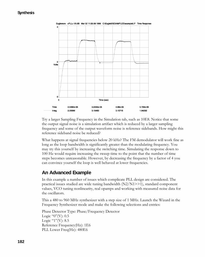
Synthesis
182
Try a larger Sampling Frequency in the Simulation tab, such as 10E8. Notice that some the output signal noise is a simulation artifact which is reduced by a larger sampling frequency and some of the output waveform noise is reference sidebands. How might this reference sideband noise be reduced?
What happens at signal frequencies below 20 kHz? The FM demodulator will work fine as long as the loop bandwidth is significantly greater than the modulating frequency. You may try this yourself by increasing the switching time. Simulating the response down to 100 Hz would require increasing the sweep time to the point that the number of time steps becomes unreasonable. However, by decreasing the frequency by a factor of 4 you can convince yourself the loop is well behaved at lower frequencies.
An Advanced Example In this example a number of issues which complicate PLL design are considered. The practical issues studied are wide tuning bandwidth (N2/N1>>1), standard component values, VCO tuning nonlinearity, real opamps and working with measured noise data for the oscillators.
This a 480 to 960 MHz synthesizer with a step size of 1 MHz. Launch the Wizard in the Frequency Synthesizer mode and make the following selections and entries:
Phase Detector Type: Phase/Frequency Detector Logic “0”(V): 0.5 Logic “1”(V): 8.5 Reference Frequency(Hz): 1E6 PLL Lower Freq(Hz): 480E6
PLL
183
PLL Upper Freq(Hz): 960E6 VCO Freq Min(Hz): 440E6 VCO Freq Max(Hz): 1000E6 VCO Voltage for Fmin(V): 0.5 VCO V for Fmax(V): 8.5 Opamp Positive Clip(V): 15 Negative Clip(V): -15 Loop BW(Hz): 50000 Loop Filter Type: 4-Pole Prefiltered Loop Filter Capacitor C1(F): 3.3E-9 Extra Loop Filter?: No Phase Margin(degrees): 60
Next, overwrite these values selected by the Wizard:
Sim: Freq Plot Minimum Frequency(Hz): 10 Sim: Time Plot Maximum Time(S): 0.002 Sim: Time Plot Sample Frequency(Hz): 5E7 Sim: Test Conditions Switching Time(S): 0.0007 PD/÷:Phase/Frequency Det Noise Floor(dBc/Hz):-155 VCO: Loaded Q: 10
Next turn on the “Use Tuning Table” option and click on the Edit Data button. Enter the following values of VCO frequency versus tuning voltage:
#1 440.0E6 0.5 #2 531.3E6 1.5 #3 616.5E6 2.5 #4 695.7E6 3.5 #5 768.7E6 4.5 #6 835.7E6 5.5 #7 896.6E6 6.5 #8 951.4E6 7.5 #9 1000E6 8.5
Next, select the noise plots in the Frequency domain output window. The results are given here.
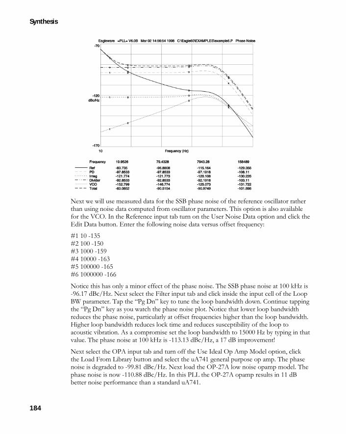
Synthesis
184
Next we will use measured data for the SSB phase noise of the reference oscillator rather than using noise data computed from oscillator parameters. This option is also available for the VCO. In the Reference input tab turn on the User Noise Data option and click the Edit Data button. Enter the following noise data versus offset frequency:
#1 10 -135 #2 100 -150 #3 1000 -159 #4 10000 -163 #5 100000 -165 #6 1000000 -166
Notice this has only a minor effect of the phase noise. The SSB phase noise at 100 kHz is -96.17 dBc/Hz. Next select the Filter input tab and click inside the input cell of the Loop BW parameter. Tap the “Pg Dn” key to tune the loop bandwidth down. Continue tapping the “Pg Dn” key as you watch the phase noise plot. Notice that lower loop bandwidth reduces the phase noise, particularly at offset frequencies higher than the loop bandwidth. Higher loop bandwidth reduces lock time and reduces susceptibility of the loop to acoustic vibration. As a compromise set the loop bandwidth to 15000 Hz by typing in that value. The phase noise at 100 kHz is -113.13 dBc/Hz, a 17 dB improvement!
Next select the OPA input tab and turn off the Use Ideal Op Amp Model option, click the Load From Library button and select the uA741 general purpose op amp. The phase noise is degraded to -99.81 dBc/Hz. Next load the OP-27A low noise opamp model. The phase noise is now -110.88 dBc/Hz. In this PLL the OP-27A opamp results in 11 dB better noise performance than a standard uA741.
PLL
185
Notice that at offsets higher than 1 kHz the predominant noise sources are the integrator (with the opamp), the phase detector and the divider. Noise from these sources can be filtered well above the loop bandwidth using an extra loop filter. Select the Filter input tab and add an elliptic lowpass filter with order = 3, passband ripple = 0.1, stopband attenuation = 30 and a cutoff frequency of 60000 Hz. The phase noise at 100 kHz is now -120.44 dBc/Hz, over 24 dB better than the original design! The phase noise at offsets higher than 125 kHz is now limited by the VCO.
Next we will examine the effect of standard element values in the loop filter. In the Filter input tab turn on the Override option for the loop filter elements and enter the following standard values:
C1(F): 3.3E-9 C2(F): 8.2E-7 C3(F): 5.6E-8 R1(ohms): 220 R2(ohms): 47
The effect of these changes was minimal. Next we will examine the effect of tuning the loop from 480 to 960 MHz by adjusting N. First, increase the number of points per decade in the Simulation input tab Frequency Plot section from 10 to 50. Normally when N is changed PLL automatically recomputes the loop filter element values. However, remember that we have fixed the element values in the Filter tab on standard values.
Next select the PD/÷ input tab. The original values were computed by PLL at the average N value of 720 now displayed in the Divider N cell. Changing N will now have the same effect as changing N to tune the synthesizer. Change Divider N from 720 to 980. Because N effects the gain of the loop, the phase noise changes with N. Next change N to 480. Severe peaking (approximately 8 dB) occurs in the noise responses. N1 = 1/2 of N2, in combination with a VCO gain at 480 MHz which is significantly higher than at 960 MHz, results in an open loop gain at 480 MHz which is nearly four times as great as at 960 MHz, threatening loop stability.
Notice that the Status button is yellow. Clicking on the Status button reveals that the extra loop filter is too close to the loop bandwidth. This has contributed to the poor stability of the loop. Change the extra loop filter to a cutoff frequency of 100 kHz. This significantly reduces the phase noise peaking at N = 480. Return N to 720 in the PD/÷ input tab. The SSB phase noise after these changes is given here.

Synthesis
186
Next, select Loop Response in the Frequency domain output window. Set N in the PD/÷ input tab to 960. Notice the open loop bandwidth is approximately 8.3 kHz. Set N to 480. The loop bandwidth is now approximately 26 kHz. This variation is a major cause of the phase noise and stability changes with N.
Next select the Time domain tab in the output window, click Recalc, turn on only the Integrator response and click Autoscale. Notice that much of the lock time is a near linear ramp time charging the integrator via the phase detector. Reducing the loop bandwidth has significantly slowed the lock time. Put the extra loop filter back at 60 kHz and Recalc. Notice the ringing near lock at N=480 (the lowest voltage and frequency) is greater than the ringing at N = 960. Can you guess why this is so?
The Status button is green. This is a reminder that we have left the loop filter element values at fixed values which will not be changed if we redesign the loop.

PLL
187
PLL: Reference
Main Window Overview
PLL is started by clicking on its icon in the Eagleware group. When you start PLL, you will see a screen similar to the one above. The main window contains the following items:
Menu bar - The menu bar near the top of the screen is used for starting a new PLL, loading or saving files, printing, running examples, and starting the wizard. The options are described in more detail later in this section.
Input tabs - The left part of the main window contains the input tabs and prompts. All inputs are typed into this area. These inputs are grouped into tabs that are selected by clicking the mouse on the tab name. For details on specific tabs and prompts, see the Input Tab section later in this section.
Note: Inputs may be tuned using PgUp and PgDn for quick changes. See “Tuning Percentage” later in this section.
Output windows - The right part of the main window contains all PLL output. Like the input area, the output window is segmented into tabbed sections. For details on specific output windows, see the output window section later in this section.
Status line - The bottom part of the main window contains current status information. The cursor readout gives precise values on the graphs at the current mouse pointer location.
The status button lights up green (info), yellow (warning), red (error), or black (fatal error) when messages are available. Click this button to view the messages. For details on the meaning of a particular message, see the PLL Messages section.
Note: Pay careful attention to the status button, especially if it is lit up red or black. The messages often answer the question, “Why doesn’t my PLL work?”
Synthesis
188
The tuning percentage is the amount that an input will be changed by pressing PgUp or PgDn. Tuning allows a numeric input in PLL to be rapidly adjusted to see the effects. To tune a value, move the cursor to the prompt and press PgUp and PgDn. All output windows (except the Time tab) will be updated immediately. To change the tuning percentage itself, press F7 and F9.
Menu Bar The menu bar at the top of the PLL main window contains the File, Examples, Wizard, and Help menus.
File Menu New (Change type) - displays a list of available PLL types. For information on PLL concepts, see the Phase-Locked Loop Concepts section.
Open file - loads a previously saved PLL setup file. These files generally have a .PL$ extension. This setup file contains all PLL inputs. Additionally, PLL automatically saves the current setup to DEFAULT.PL$ whenever PLL is exited. When PLL is restarted, DEFAULT.PL$ is automatically loaded. This file causes PLL to “remember” your last inputs, so saving a PL$ file is only necessary for permanent archival of setups.
Save - saves the current setup file. If the file has not been named, a save file dialog box will appear asking for the file name.
Save As - saves the current setup file. A save file dialog box will appear asking for the file name.
Toggle Background Color - toggles the background color of the graphs between black and white. This can be especially useful before printing a screen dump.
Print/Plot/Export Time Response - sends the time response graph to a printer or to a Windows metafile (WMF).
Print/Plot/Export Frequency Response - sends the frequency response graph to a printer or to a Windows metafile (WMF).
Print/Plot/Export Schematic - sends the schematic graph to a printer or to a Windows metafile (WMF).
Print Report - sends the contents of the Report output window to a printer.
Print Screen - sends a picture of the entire screen to a printer or to a Windows bitmap (BMP) file.
Print Window - sends a picture of the active window to a printer or to a Windows bitmap (BMP) file.
Note: The Print Screen and Print Window items send the picture at the same quality as seen on the screen. For a higher resolution printout, select one of the first four print/plot/export items.
Exit - quits PLL.
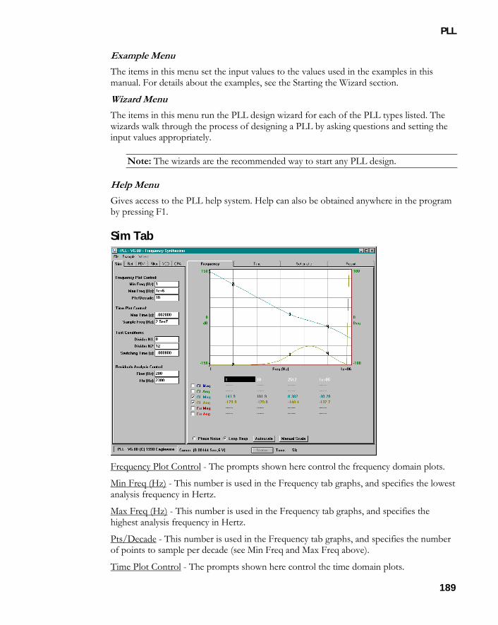
PLL
189
Example Menu The items in this menu set the input values to the values used in the examples in this manual. For details about the examples, see the Starting the Wizard section.
Wizard Menu The items in this menu run the PLL design wizard for each of the PLL types listed. The wizards walk through the process of designing a PLL by asking questions and setting the input values appropriately.
Note: The wizards are the recommended way to start any PLL design.
Help Menu Gives access to the PLL help system. Help can also be obtained anywhere in the program by pressing F1.
Sim Tab
Frequency Plot Control - The prompts shown here control the frequency domain plots.
Min Freq (Hz) - This number is used in the Frequency tab graphs, and specifies the lowest analysis frequency in Hertz.
Max Freq (Hz) - This number is used in the Frequency tab graphs, and specifies the highest analysis frequency in Hertz.
Pts/Decade - This number is used in the Frequency tab graphs, and specifies the number of points to sample per decade (see Min Freq and Max Freq above).
Time Plot Control - The prompts shown here control the time domain plots.
Synthesis
190
Max Time (s) - This number is used in the Time window plots, and specifies the simulation time in seconds.
Sample Freq (Hz) - This number is used in the Time window plots, and specifies the sampling frequency in Hertz.
The sampling frequency determines the distance between time steps. This number is very important for time domain simulations. In most cases, the sampling frequency should be at least a few hundred times the reference frequency and a few thousand times the loop bandwidth for an accurate simulation. This is because the phase detector pulses are typically very narrow in relation to the reference period, and under-sampling discretization of the pulse widths can lead to an inaccurate simulation.
The total number of points in a simulation is given by:
Number of Points=(Simulation time)x(Sampling Frequency)
Note: The time domain simulation requires approximately 80 bytes of RAM per point. For instance, 500000 points will require about 40M of memory.
One factor which does not need to be considered in choosing the sampling frequency is the actual VCO output frequency. PLL has incorporated intelligent routines that allow the VCO to be sampled much below the Nyquist rate. For instance, given a loop with a reference of 1MHz, a 1000:1 frequency divider, and a VCO of 1 GHz, a sampling rate of 100MHz is often sufficient.
Test Conditions - The prompts shown here change for each PLL type, and are used to simulate the performance of each loop type.
Phase Dev (rad) - This specifies the reference oscillator peak (±) phase deviation for use in the phase demodulator PLL. This number is used to simulate the modulated source, which is applied to the loop input.
Switching Time (s) - This is used for all loop types. The value is used as shown below:
Frequency Synthesizer PLL - specifies the time between divider ‘N’ switches. Frequency Modulator - specifies the time between the modulating square wave switches. Frequency Demodulator - specifies the time between the modulated signal’s frequency switches. Phase Modulator - specifies the time between the modulating square wave switches. Phase Demodulator - specifies the time between the modulated signal’s phase switches.
The frequency of the test signal is 1/(2 x Switch Time) in all cases.
Divider N1, Divider N2 - These numbers are used for testing the Frequency Synthesizer PLL. In time domain simulations, the digital divider is switched between N1 and N2 at the rate specified by the Switching Time prompt.
PLL
191
Peak Voltage (V) - This prompt is used in the modulator loops and specifies the peak voltage of the modulating square wave. This values ultimately determines the peak phase or frequency deviation, depending on the modulation type.
Freq Dev (Hz) - This number is used in the Frequency Modulator PLL, and specifies the amount of frequency shift applied to the carrier in each direction to form the modulated signal. For example, with a 1MHz carrier, if a frequency deviation of 100000 (100 kHz) is specified, the reference signal varies between 0.9 and 1.1 MHz.
Residuals Analysis Control - To find the phase and frequency modulation noise, the SSB phase noise must be integrated. These prompts define the interval over which the integration is to be performed. The calculated FM and PM residuals are shown on the Report tab.
Flow (Hz) - This specifies the lower frequency for the integration.
Fhi (Hz) - This specifies the upper frequency for the integration.
Ref Tab Freq (Hz) - This number specifies the reference oscillator frequency in Hertz. In frequency synthesizers, this frequency is typically chosen as the channel spacing. In modulator and demodulator applications, this frequency is generally the carrier frequency.
Load Res (ohms) - This number is used in conjunction with the oscillator output power (see Pout below) to calculate the signal level present at the phase detector input for time domain simulations.
Pout (dBm) - This number specifies the output power of the oscillator in dBm. This number is used only for phase noise calculations, and is required for Leeson’s equation.
The voltage from the reference is calculated using P=V2/R, so .
Loaded Q - This number specifies the oscillator’s loaded Q. This is only used in the phase noise calculations, and is required for Leeson’s equation. A high loaded Q reduces phase noise.
This prompt is only available if the User Noise Data box is not checked.
Flicker Corner (Hz) - This specifies the flicker corner frequency in Hertz for the active device used in the oscillator. This is the frequency at which the SSB phase noise is 3 dB higher than the oscillator noise floor. A typical value is 10 kHz.
This prompt is only available if the User Noise Data box is not checked.
Noise Figure (dB) - This number specifies the active device noise figure in dB. This is used only in the phase noise calculations.
This prompt is only available if the User Noise Data box is not checked.
User Noise Data (Checkbox) - This button allows measured data to be entered as the oscillator SSB phase noise.
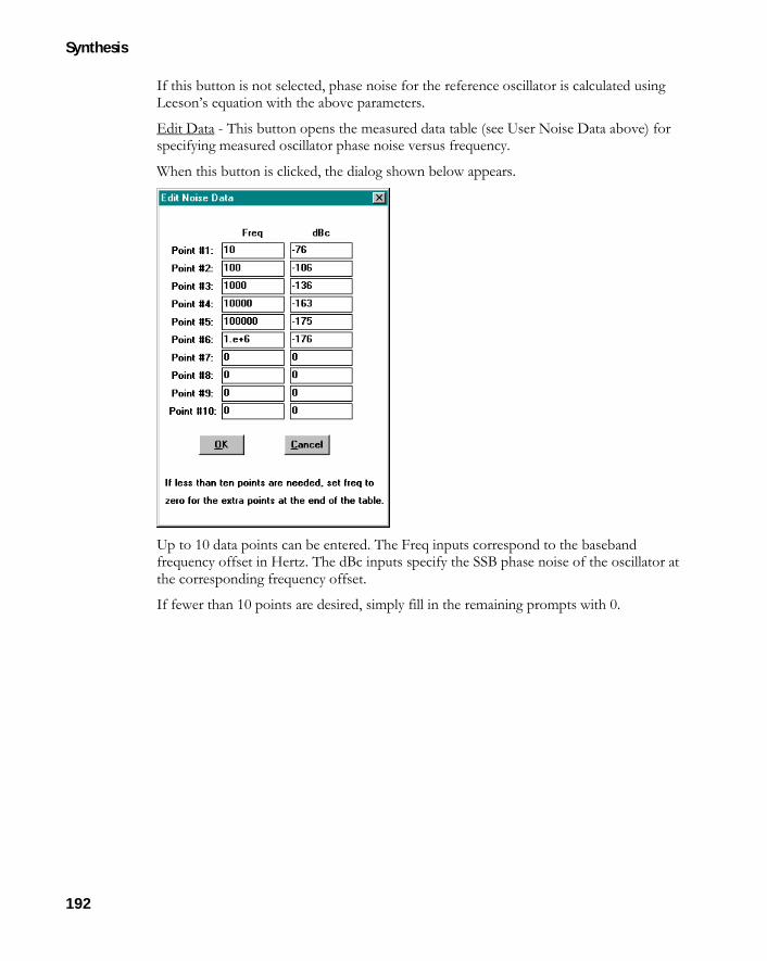
Synthesis
192
If this button is not selected, phase noise for the reference oscillator is calculated using Leeson’s equation with the above parameters.
Edit Data - This button opens the measured data table (see User Noise Data above) for specifying measured oscillator phase noise versus frequency.
When this button is clicked, the dialog shown below appears.
Up to 10 data points can be entered. The Freq inputs correspond to the baseband frequency offset in Hertz. The dBc inputs specify the SSB phase noise of the oscillator at the corresponding frequency offset.
If fewer than 10 points are desired, simply fill in the remaining prompts with 0.
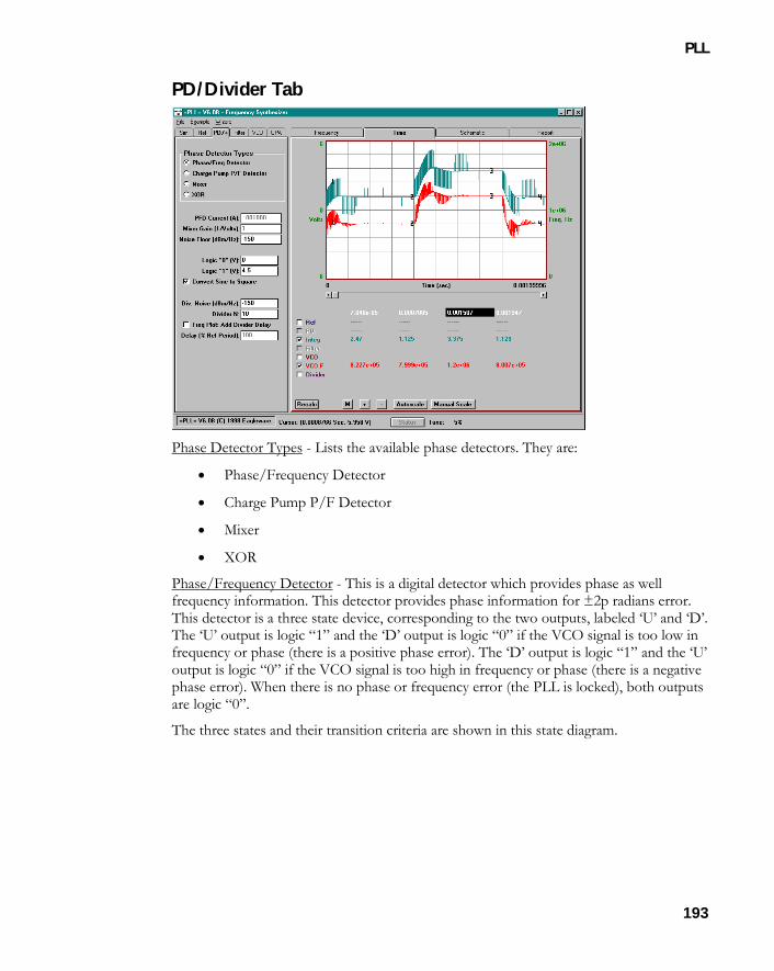
PLL
193
PD/Divider Tab
Phase Detector Types - Lists the available phase detectors. They are:
• Phase/Frequency Detector
• Charge Pump P/F Detector
• Mixer
• XOR
Phase/Frequency Detector - This is a digital detector which provides phase as well frequency information. This detector provides phase information for ±2p radians error. This detector is a three state device, corresponding to the two outputs, labeled ‘U’ and ‘D’. The ‘U’ output is logic “1” and the ‘D’ output is logic “0” if the VCO signal is too low in frequency or phase (there is a positive phase error). The ‘D’ output is logic “1” and the ‘U’ output is logic “0” if the VCO signal is too high in frequency or phase (there is a negative phase error). When there is no phase or frequency error (the PLL is locked), both outputs are logic “0”.
The three states and their transition criteria are shown in this state diagram.

Synthesis
194
Frequency correction in this type of detector is provided by the current state (‘U’, ‘D’, or neither). Phase correction is provided by pulse width modulation of the outputs. In other words, the pulse widths get smaller as the PLL nears lock.
The gain of the phase/frequency detector is given by:
Kd = ((Logic "1" Voltage) - (Logic "0" Voltage)) / (2*pi)
The logic voltages are specified in the PD/Divider tab.
Charge Pump P/F Detector - This detector is identical to the Phase/Frequency detector except that it has a a single current output instead of two voltages. A diagram of the additional current buffers is shown here.
The gain of the this type of detector is given by:
where Imax is the current specified in the "PFD Current" prompt.
In some charge pump detectors, the output current is programmable, which allows lower power consumption by the integrated circuit. Since the integrator must produce an output voltage which drives the VCO over the PLL’s frequency range, a lower current from the detector simply raises the impedances needed in the integrator. Conversely, a higher current lowers the integrator impedance levels.

PLL
195
Mixer - This selects an ideal mixer as the phase detector. Mixers provide phase error information, but do not provide frequency error information. For this reason, a PLL using a mixer phase detector does not have a wide lock range, and often needs assistance acquiring lock initially. This can be done in several ways, the most obvious of which is to force the VCO to output a specific frequency on power-up.
The mathematical model used in PLL for a mixer is:
where v1 and v2 represent the mixer input signals, Thetae is the phase difference between the inputs, and Km is a gain constant associated with the mixer. This constant is usually set to “1” if the mixer is passive.
The actual phase detector gain for a mixer is:
where Km is specified as above, and V1 and V2 in this equation represent the peak voltages present at the mixer inputs.
XOR - This selects an XOR gate as the phase detector. An XOR is a simple logic gate which provides phase error information only (similar to the mixer). The truth table for the PLL XOR model is shown in below.
Input #1
Input #2
Output #1
Output #2
0 0 0 1
0 1 1 0
1 0 1 0
1 1 0 1
The phase detector gain for the XOR is:
Kd = ((Logic "1" Voltage) - (Logic "0" Voltage)) / (pi/2)
PFD Current (A) - This specifies the maximum output current for the charge pump phase detector. This number is assumed to be symmetric in the push/pull current buffers. In other words, the ‘U’ and ‘D’ states produce positive and negative currents equal in magnitude to the number specified in this prompt.
A typical value is 2 mA.
Mixer Gain (1/Volts) - This number specifies the Km discussed in the Mixer section. This is not the phase detector gain, but simply the forward gain of the mixer itself. This number is typically 1 for a passive device such as a ring diode mixer.
Noise Floor (dB) - This specifies the phase detector noise floor in dBc/Hz. This number is assumed to be flat for all phase offsets. A typical value is -150.
Synthesis
196
Logic “0” (V), Logic “1” (V) - These numbers are the internal values to use for logic “0” and “1”. In most digital circuits, the logic levels are not equal to the supply rails. For example, a LSTTL chip with a +5 volt supply typically has about +4.5 volts for a good “1”, and about +0.5 for a good “0”.
Convert Sine to Square - When enabled, this option forces digital blocks (e.g. divider and digital phase detector) to convert each input to a digital logic level. This is important for circuits where analog signals must be fed into digital blocks. For example, if the VCO output peak voltage present at the digital divider is less than the required logic switching voltage, the divider will never count. In this case, the loop cannot lock. Selecting this option will convert all voltages<=0 to a logic “0”, while all voltages>0 become a logic “1”. This is essentially a 1 bit A/D conversion.
If a loop is to be designed with digital parts which do not contain the A/D conversion mentioned above, the “Convert” option should be disabled. This will allow PLL to model the actual logic device switching for an analog input. Even if the VCO output voltage covers the required switching range for the divider, different results will be obtained when the “Convert” option is enabled or disabled. To understand why, consider a ±5 volt sine wave input to a TTL level inverter. The inverter’s square wave output will not have a 50% duty cycle since the sine wave spends only about 17% of the time greater than or equal to the required “1” voltage level.
Divider Noise Floor - This number specifies the noise floor to use for the digital frequency divider in dBc/Hz. A typical value is -150.
Divider N - This number specifies the divider ‘N’ value to use in the calculation of the integrator components. Loops are typically designed for an ‘N’ that is roughly mid-way between the highest and lowest values that the loop must obtain lock for. For example, to design a frequency demodulator for the FM radio band (88-108 MHz), the divider ‘N’ should be placed at the value which corresponds to a VCO output frequency of 98 MHz.
Note: To remove the divider from the loop, enter 1 for Divider N.
Freq Plot: Add Divider Delay - This option adds divider delay to the responses shown in the Frequency window. The divider counts cycles from the VCO and toggles its output once every N ticks. During this time, the phase detector is unable to respond immediately to VCO outputs, resulting in what is called divider delay.
Delay (% Ref Period) - This number specifies the amount of delay (as a percentage of the reference period) to introduce into the frequency plots. There is wide dispute about how much divider delay is actually present in a given system, so this prompt has been left for the user to decide.
Fifty percent of the reference period is a typical value for the divider delay.
Turning this delay on or off has no effect on the time domain simulation. Since the time domain simulation models transient behavior, sampling delay and divider delay are inherently included.
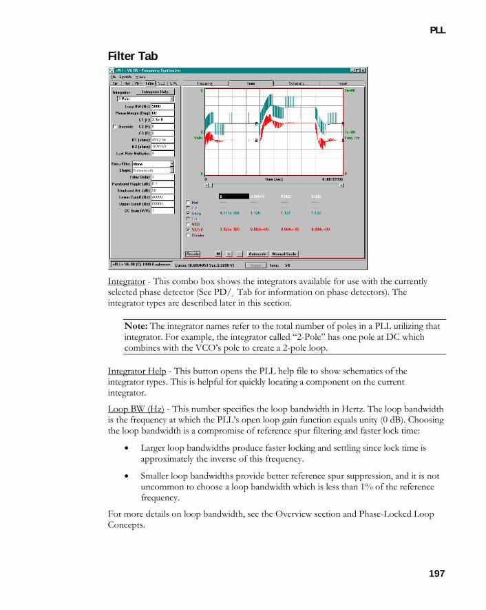
PLL
197
Filter Tab
Integrator - This combo box shows the integrators available for use with the currently selected phase detector (See PD/¸ Tab for information on phase detectors). The integrator types are described later in this section.
Note: The integrator names refer to the total number of poles in a PLL utilizing that integrator. For example, the integrator called “2-Pole” has one pole at DC which combines with the VCO’s pole to create a 2-pole loop.
Integrator Help - This button opens the PLL help file to show schematics of the integrator types. This is helpful for quickly locating a component on the current integrator.
Loop BW (Hz) - This number specifies the loop bandwidth in Hertz. The loop bandwidth is the frequency at which the PLL’s open loop gain function equals unity (0 dB). Choosing the loop bandwidth is a compromise of reference spur filtering and faster lock time:
• Larger loop bandwidths produce faster locking and settling since lock time is approximately the inverse of this frequency.
• Smaller loop bandwidths provide better reference spur suppression, and it is not uncommon to choose a loop bandwidth which is less than 1% of the reference frequency.
For more details on loop bandwidth, see the Overview section and Phase-Locked Loop Concepts.
Synthesis
198
Phase Margin (Deg) - This number specifies the loop phase margin in degrees. The phase margin is equal to 180 degrees minus the open loop phase at the loop bandwidth frequency and should normally be greater than 30 degrees for ensured loop stability.
Several factors can degrade the actual phase margin observed in a loop:
1. If specified, an extra filter adds phase inside the loop bandwidth which decreases the phase margin. Increasing its cutoff frequency or decreasing the filter order will improve the phase margin.
2. The VCO RC bandwidth (1/2pRC) is too close to the loop bandwidth. Since the VCO “bandwidth” is modeled as a simple RC filter, it has the same effect as adding a first order extra loop filter. Increasing its bandwidth may improve the phase margin.
3. The non-ideal op amp model adds phase inside the loop bandwidth. This can be caused by many of the parameters in the op amp tab. If selecting “Use Ideal Op Amp Model” improves the phase margin, a different op amp may be needed to stabilize the loop.
C1 (F) - This box shows the current value for the integrator capacitor C1. See the individual integrator schematics for a definition of this component.
Note: Changing C1 can have a dramatic effect on both phase noise performance and phase detector power requirements. See the Frequency Synthesizer example and the Advanced Example for more details.
Override (Checkbox) - This allows user entry of all integrator component values. When this box is checked, the component values are editable. The loop bandwidth and phase margin input boxes are not selectable when components are overridden since they will not be used in calculations.
Note: The override checkbox can also be used to modify input parameters without changing the loop. For example, when override is checked, the divider N can be changed without PLL automatically compensating the loop filter.
C2, C3 (F) - This box shows the current value for the integrator capacitors C2 and C3. See the individual integrator schematics for a definition of this component. If this component is not used in the current integrator, it is shown as 0. This can only be changed if Override is checked.
R1 (Ohms) - This box shows the current value for the integrator resistor R1. See the individual integrator schematics for a definition of this component. This can only be changed if Override is checked.
R2 (Ohms) - This box shows the current value for the integrator resistor R2. See the individual integrator schematics for a definition of this component. If this component is not used in the current integrator, it is shown as 0. This can only be changed if Override is checked.
PLL
199
Last Pole Multiplier - This prompt is used for the active 4-pole and passive 4-pole integrators. The last pole’s frequency is entered as multiple of the loop bandwidth. This pole multiplier is not taken into account when designing the integrator component values. Therefore, if pole is too close to the loop bandwidth (if the number entered is too close to 1), the integrator will degrade the phase margin unacceptably. This is a tradeoff between better reference sideband suppression and loop stability.
If the pole is too far outside the loop bandwidth, the integrator will behave like 3-pole integrator, adding no sideband rejection over the simpler topology.
A typical value for the last pole multiplier is 4.
Extra Filter - This option inserts a passive filter between the loop integrator and the VCO. The filter input boxes are grayed out unless this option is selected.
This filter is assumed to be an LC type, and does not contribute phase noise. However, it does add filtering to the loop phase noise.
The extra filter is not compensated for in designing the integrator component values. For this reason, loop phase margin can be degraded if too much filter phase is added near the loop bandwidth. This can introduce instability in the loop.
The options available for the extra filter are:
• None - removes the extra filter
• Lowpass Noiseless - often used to added reference sideband rejection
• Bandstop Noiseless - can be used to reject specific unwanted frequencies (such as 60 Hz). This type should be used with caution for sideband suppression, since it will not reject all harmonics of the reference oscillator
For more information on the use of an extra filter, see the Concepts section.
Shape - The available filter shapes are listed in this box. They are:
• Butterworth - has a maximally flat passband magnitude response, but adds rejection slowly in the stopband
• Chebyshev - allows ripple in the passband magnitude response, but increases attenuation quickly in the stopband
• Elliptic - (also called Cauer) has passband ripple, and increases adds transmission zeros in the stopband. It also transitions quickly into the stopband
For more information on filter shapes, see Appendix A in the Synthesis manual.
Filter Order - the order of the extra filter. Typical values are 3 and 5.
Passband Ripple (dB) - specifies the passband ripple. A typical value is 0.1.
Stopband Att (dB) - the minimum attenuation which must be maintained in the stopband (only available for Elliptic filters). A typical value is -50 dB.
Lower Cutoff (Hz) - This specifies the extra filter’s lower cutoff. For a lowpass filter, this is simply the cutoff frequency. For a Butterworth filter, this number specifies the -3 dB
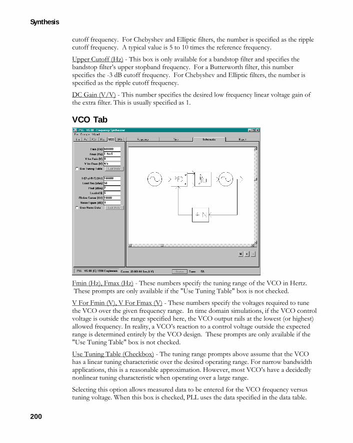
Synthesis
200
cutoff frequency. For Chebyshev and Elliptic filters, the number is specified as the ripple cutoff frequency. A typical value is 5 to 10 times the reference frequency.
Upper Cutoff (Hz) - This box is only available for a bandstop filter and specifies the bandstop filter’s upper stopband frequency. For a Butterworth filter, this number specifies the -3 dB cutoff frequency. For Chebyshev and Elliptic filters, the number is specified as the ripple cutoff frequency.
DC Gain (V/V) - This number specifies the desired low frequency linear voltage gain of the extra filter. This is usually specified as 1.
VCO Tab
Fmin (Hz), Fmax (Hz) - These numbers specify the tuning range of the VCO in Hertz. These prompts are only available if the "Use Tuning Table" box is not checked.
V For Fmin (V), V For Fmax (V) - These numbers specify the voltages required to tune the VCO over the given frequency range. In time domain simulations, if the VCO control voltage is outside the range specified here, the VCO output rails at the lowest (or highest) allowed frequency. In reality, a VCO’s reaction to a control voltage outside the expected range is determined entirely by the VCO design. These prompts are only available if the "Use Tuning Table" box is not checked.
Use Tuning Table (Checkbox) - The tuning range prompts above assume that the VCO has a linear tuning characteristic over the desired operating range. For narrow bandwidth applications, this is a reasonable approximation. However, most VCO’s have a decidedly nonlinear tuning characteristic when operating over a large range.
Selecting this option allows measured data to be entered for the VCO frequency versus tuning voltage. When this box is checked, PLL uses the data specified in the data table.

PLL
201
Edit Data - This button is only selectable if the Use Tuning Table box is checked. This button opens the VCO tuning table for editing the measured data. When this button is clicked, the dialog shown in below appears. Up to 10 data points can be entered. The Freq inputs correspond to the VCO frequency offset in Hertz. The voltage inputs specify the tuning voltage of the VCO which gives the corresponding frequency output. If fewer than 10 points are desired, simply fill in the remaining prompts with 0.
1/(2·pi·RC) (Hz) - This is sometimes called the VCO RC Bandwidth. Typically, a large isolation resistor is added to the input of a VCO for tuning purposes. When combined with the parasitic and varactor capacitance, this forms a lowpass RC pole. The number specified here is the -3 dB bandwidth of this “filter”.
The effect of this RC pole is to slow the VCO’s response to a changing control voltage. This in turn can slow the loop lock time. As the isolation resistor gets larger, this RC bandwidth decreases and the pole moves down in frequency and in extreme cases can cause loop instability.
Load Res (ohms) - This number is used in conjunction with the oscillator output power (see Pout below) to calculate the signal level present at the phase detector input for time domain simulations.
Pout (dBm) - This number specifies the output power of the oscillator in dBm. This number is used only for phase noise calculations, and is required for Leeson’s equation.
The voltage from the VCO is calculated using P=V2/R, so
Synthesis
202
Loaded Q - This number specifies the VCO’s loaded Q. This is only used in the phase noise calculations, and is required for Leeson’s equation. A high loaded Q reduces phase noise. This prompt is only available if the "User Noise Data" box is not checked.
Flicker Corner (Hz) - This specifies the flicker corner frequency in Hertz for the active device contained in the oscillator. This is the frequency at which the SSB phase noise is 3 dB higher than the oscillator noise floor. A typical value is 10 kHz. This prompt is only available if the "User Noise Data" box is not checked.
Noise Figure (dB) - This number specifies the active device noise figure in dB. This is used only in the phase noise calculations. This prompt is only available if the "User Noise Data" box is not checked.
User Noise Data (Checkbox) - This button allows measured data to be entered as the oscillator SSB phase noise.
Edit Data - This button opens the measured data table (see User Noise Data above) for specifying measured oscillator SSB phase noise versus frequency. Up to 10 data points can be entered. The Freq inputs correspond to the baseband frequency offset in Hertz. The dBc inputs specify the SSB phase noise of the oscillator at the corresponding frequency offset. If fewer than 10 points are desired, simply fill in the remaining prompts with 0.
OPA Tab Name - This is the name used in the library file to identify the op amp data. Whenever a parameter has been changed, this prompt changes to “Custom”.
Whenever an op amp is saved to the library, PLL prompts for a name to assign to the data. The name is used later to display in this prompt.
Rin (ohms) - the input resistance of the op amp. For bipolar transistors, this is usually about 1 MOhm. For op amps with JFET input stages, 1 TOhm (1012 Ohm) is typical.
Rout (ohms) - This specifies the op amp output resistance. A typical value is 75 Ohm.
DC O.L Gain (V/V) - This specifies the DC open loop gain in volts/volt. A typical value is 50000.
0 dB Freq (Hz) - This specifies the unity gain crossover frequency in Hertz. This is also called the gain-bandwidth product. This is the frequency at which the op amp open loop gain has fallen to 1 (0 dB). A typical value is 4 MHz.
Noise Voltage (V) - This is the noise voltage density. This is also called the equivalent noise voltage (ven). The units are typically given as nV/sqrt(Hz). Since PLL assumes a 1 Hz noise bandwidth, the sqrt(Hz) can be ignored. A typical number is 20 nV.
Noise Current (A) - This is the noise current density. This is also called the equivalent noise current (ien). The units are typically given as pA/sqrt(Hz). Since PLL assumes a 1 Hz noise bandwidth, the sqrt(Hz) can be ignored. A typical number is 0.7 pA.

PLL
203
Offset Voltage (V) - Real op amps have a nonzero output voltage when the inputs are zero. This can be modeled by a constant voltage at the input terminals. This is called the offset voltage. A typical value is 10 uV.
Offset Current (A) - Real op amps have a nonzero output current when the inputs are zero. This can be modeled by a constant current at the input terminals. This is called the offset current. A typical value is 1 nA.
Bias Current (A) - This is the DC current that flows into the inputs of the opamp. For opamps with a bipolar input stage, a typical value is 1 uA. For opamps with a JFET input stage, a typical value is 1pA (10-12 A).
PSRR (dB) - This number is the power supply rejection ratio in dB. This number is the change in the op amp output for a given change in the supply voltage. A typical value is 100 dB.
Use Ideal Op Amp Model - This forces PLL to use ideal parameters internally for the op amp model. This is useful for several reasons:
• If a PLL isn’t locking, selecting this option and re-simulating quickly determines if the op amp is the problem.
• If this option is used when plotting phase noise, the op amp is quiet, so that the noise produced by an active integrator comes only from the resistors.
• This allows quick comparison between locking with a real op amp and an ideal one.
Load From Lib - loads a pre-saved op amp from the library.
Save To Lib - saves the current op amp data to the library.
Note: The library is stored in OPAMP.DAT
Pos Clip (V) - This specifies the highest voltage which the op amp can output. This is typically at least 1 volt below the positive supply.
Neg Clip (V) - This specifies the lowest voltage which the op amp can output. This is typically at least 1 volt above the negative supply.
Supply Ripple (V) - This specifies the amount of ripple on the supply line in volts. This value is used in conjunction with the PSRR to model the non-ideal change in the op amp’s output with a changing supply level.
Output Tabs & Graphs The output tabs contain all calculated results from PLL. These results are grouped into tabs that are selected by clicking the mouse on the tab name. The Frequency, Schematic, and Report tabs are automatically recalculated whenever an input is changed; the Time tab is only recalculated when the Recalc button is pressed.
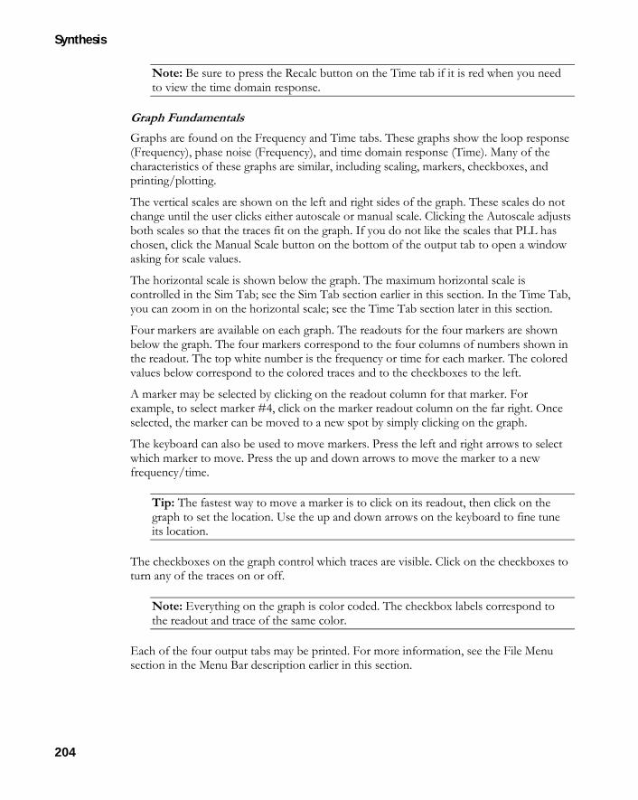
Synthesis
204
Note: Be sure to press the Recalc button on the Time tab if it is red when you need to view the time domain response.
Graph Fundamentals Graphs are found on the Frequency and Time tabs. These graphs show the loop response (Frequency), phase noise (Frequency), and time domain response (Time). Many of the characteristics of these graphs are similar, including scaling, markers, checkboxes, and printing/plotting.
The vertical scales are shown on the left and right sides of the graph. These scales do not change until the user clicks either autoscale or manual scale. Clicking the Autoscale adjusts both scales so that the traces fit on the graph. If you do not like the scales that PLL has chosen, click the Manual Scale button on the bottom of the output tab to open a window asking for scale values.
The horizontal scale is shown below the graph. The maximum horizontal scale is controlled in the Sim Tab; see the Sim Tab section earlier in this section. In the Time Tab, you can zoom in on the horizontal scale; see the Time Tab section later in this section.
Four markers are available on each graph. The readouts for the four markers are shown below the graph. The four markers correspond to the four columns of numbers shown in the readout. The top white number is the frequency or time for each marker. The colored values below correspond to the colored traces and to the checkboxes to the left.
A marker may be selected by clicking on the readout column for that marker. For example, to select marker #4, click on the marker readout column on the far right. Once selected, the marker can be moved to a new spot by simply clicking on the graph.
The keyboard can also be used to move markers. Press the left and right arrows to select which marker to move. Press the up and down arrows to move the marker to a new frequency/time.
Tip: The fastest way to move a marker is to click on its readout, then click on the graph to set the location. Use the up and down arrows on the keyboard to fine tune its location.
The checkboxes on the graph control which traces are visible. Click on the checkboxes to turn any of the traces on or off.
Note: Everything on the graph is color coded. The checkbox labels correspond to the readout and trace of the same color.
Each of the four output tabs may be printed. For more information, see the File Menu section in the Menu Bar description earlier in this section.
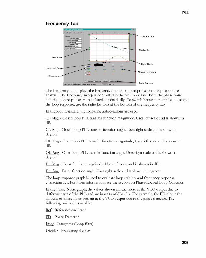
PLL
205
Frequency Tab
The frequency tab displays the frequency domain loop response and the phase noise analysis. The frequency sweep is controlled in the Sim input tab. Both the phase noise and the loop response are calculated automatically. To switch between the phase noise and the loop response, use the radio buttons at the bottom of the frequency tab.
In the loop response, the following abbreviations are used:
CL Mag - Closed loop PLL transfer function magnitude. Uses left scale and is shown in dB.
CL Ang - Closed loop PLL transfer function angle. Uses right scale and is shown in degrees.
OL Mag - Open loop PLL transfer function magnitude, Uses left scale and is shown in dB.
OL Ang - Open loop PLL transfer function angle. Uses right scale and is shown in degrees.
Err Mag - Error function magnitude, Uses left scale and is shown in dB.
Err Ang - Error function angle. Uses right scale and is shown in degrees.
The loop response graph is used to evaluate loop stability and frequency response characteristics. For more information, see the section on Phase-Locked Loop Concepts.
In the Phase Noise graph, the values shown are the noise at the VCO output due to different parts of the PLL and are in units of dBc/Hz. For example, the PD plot is the amount of phase noise present at the VCO output due to the phase detector. The following traces are available:
Ref - Reference oscillator
PD - Phase Detector
Integ - Integrator (Loop filter)
Divider - Frequency divider
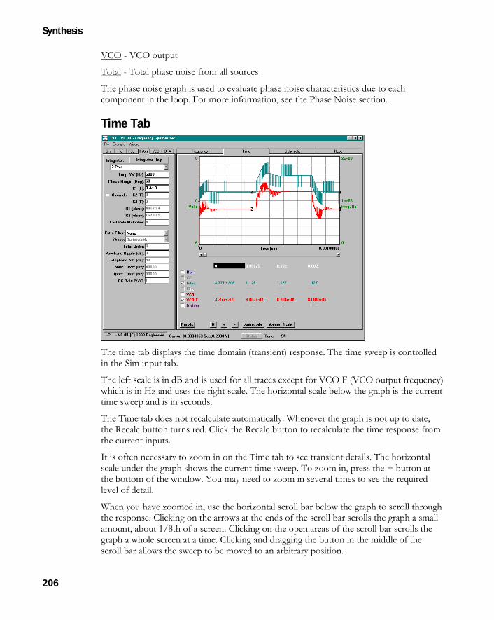
Synthesis
206
VCO - VCO output
Total - Total phase noise from all sources
The phase noise graph is used to evaluate phase noise characteristics due to each component in the loop. For more information, see the Phase Noise section.
Time Tab
The time tab displays the time domain (transient) response. The time sweep is controlled in the Sim input tab.
The left scale is in dB and is used for all traces except for VCO F (VCO output frequency) which is in Hz and uses the right scale. The horizontal scale below the graph is the current time sweep and is in seconds.
The Time tab does not recalculate automatically. Whenever the graph is not up to date, the Recalc button turns red. Click the Recalc button to recalculate the time response from the current inputs.
It is often necessary to zoom in on the Time tab to see transient details. The horizontal scale under the graph shows the current time sweep. To zoom in, press the + button at the bottom of the window. You may need to zoom in several times to see the required level of detail.
When you have zoomed in, use the horizontal scroll bar below the graph to scroll through the response. Clicking on the arrows at the ends of the scroll bar scrolls the graph a small amount, about 1/8th of a screen. Clicking on the open areas of the scroll bar scrolls the graph a whole screen at a time. Clicking and dragging the button in the middle of the scroll bar allows the sweep to be moved to an arbitrary position.
PLL
207
To zoom back out incrementally, use the - (minus) button at the bottom of the window. To zoom all the way out in one click, press the M button (maximize).
Schematic Tab
The schematic tab shows the current PLL block diagram. The schematic updates automatically whenever input prompts change. The symbols shown used on the schematic tab are shown above. Most symbols are standard electronic symbols, but a few were custom designed for PLL. All of them should be self-explanatory.
The schematic contains all information needed to build the PLL. You can print the schematic (select Print/Plot/Export schematic from the file menu) to get a block diagram for use in documentation. The details for each block are contained in the Report tab.
You can also get details about any symbol in the schematic by clicking on it. Clicking on the symbol brings up a dialog box with all values used to simulate that symbol. For example, clicking on the VCO gives the Designator, peak output voltage, up to ten tuning points on the voltage vs. frequency curve, 1/(2piRC) (also called RC bandwidth), and the optional DC Offset Voltage (always zero in PLL). Pressing escape or clicking the OK button closes the dialog box.
The schematic also can be scrolled (using the scroll bars) and zoomed (using the M, +, and - buttons) if necessary.
Report Tab The report tab contains a text box with all of the details necessary to recreate the PLL setup or to build the real PLL. It is probably the most important data in PLL for use in engineering documentation. It is also handy if a setup needs to be Faxed to Eagleware for Technical support. You can print the report by selecting Print Report from the File menu.

Synthesis
208
Tip: If you contact Eagleware electronically for technical support, be sure to include a printout of the report (if contacting by fax) or a copy of the setup file (PL$) which you have saved (if contacting by email).
On most monitors, the report will be more than one page long. To see the entire report, you must scroll using either the scroll bar on the right or the keyboard cursor keys.
You can cut and paste the contents of the report window for use in your word processor or other electronic use. Right click on the report and choose Select All from the pop-up menu. Next, right click on the report again and choose Copy from the pop-up menu. Now, go into your word processor and paste the text, generally by selecting Paste from the edit menu.
Report Contents The report has the following contents:
Header - Date and time that the report was created plus PLL copyright information.
Filename - The name of the current setup file (PL$). Note: This will only be present if a setup file has been saved.
PLL Type - The basic class of PLL application.
Loop Statistics - General loop data including: Residuals (See the Sim tab for controls), VCO center frequency, VCO gain at the center frequency, and approximate lock time in seconds.
Schematic Element Details - Gives complete details for all blocks shown on the schematic tab. These values should be used when building the PLL. For example, the Integrator (Designator: Integ) section contains the component values for the loop filter (integrator).
Input Parameters - Gives a complete list of all input parameters, grouped by input tab. If a value is shown as N/A, then the input prompt was greyed out and has no bearing on the current design.
Note: In the Filter tab section on the report, the components C2, C3, R1, and R2 are always shown as N/A unless the Override button is checked. To find these component values on the report, look at the integrator in Schematic Element Details earlier in the report.
Integrators
2-Pole
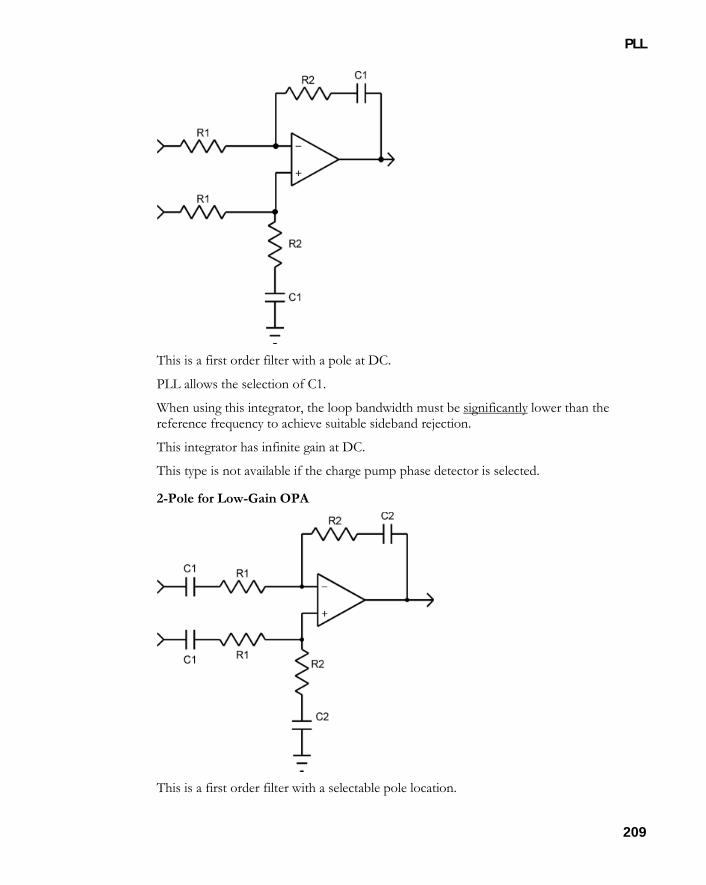
PLL
209
This is a first order filter with a pole at DC.
PLL allows the selection of C1.
When using this integrator, the loop bandwidth must be significantly lower than the reference frequency to achieve suitable sideband rejection.
This integrator has infinite gain at DC.
This type is not available if the charge pump phase detector is selected.
2-Pole for Low-Gain OPA
This is a first order filter with a selectable pole location.
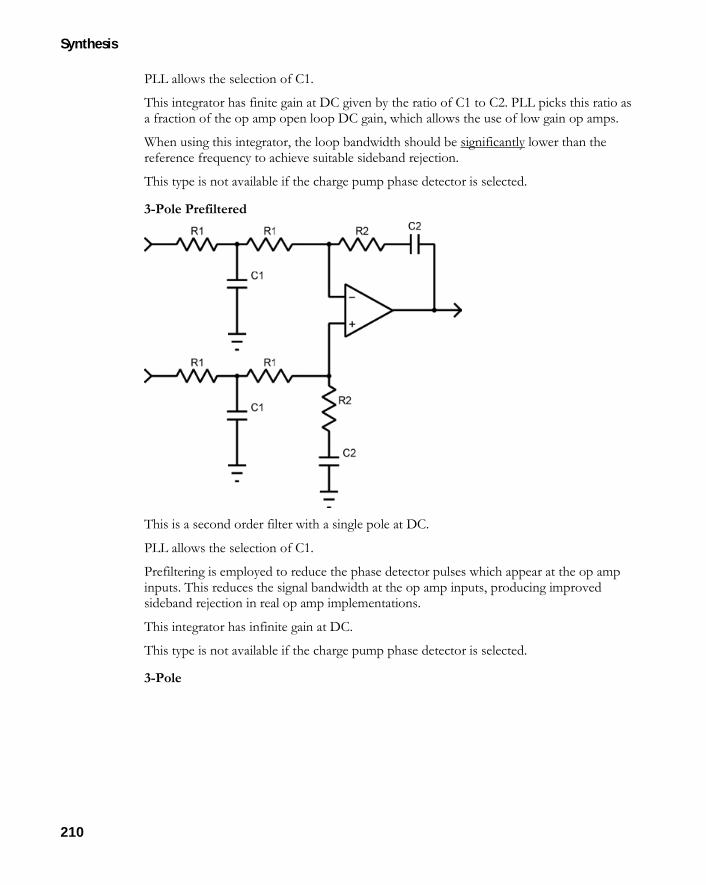
Synthesis
210
PLL allows the selection of C1.
This integrator has finite gain at DC given by the ratio of C1 to C2. PLL picks this ratio as a fraction of the op amp open loop DC gain, which allows the use of low gain op amps.
When using this integrator, the loop bandwidth should be significantly lower than the reference frequency to achieve suitable sideband rejection.
This type is not available if the charge pump phase detector is selected.
3-Pole Prefiltered
This is a second order filter with a single pole at DC.
PLL allows the selection of C1.
Prefiltering is employed to reduce the phase detector pulses which appear at the op amp inputs. This reduces the signal bandwidth at the op amp inputs, producing improved sideband rejection in real op amp implementations.
This integrator has infinite gain at DC.
This type is not available if the charge pump phase detector is selected.
3-Pole
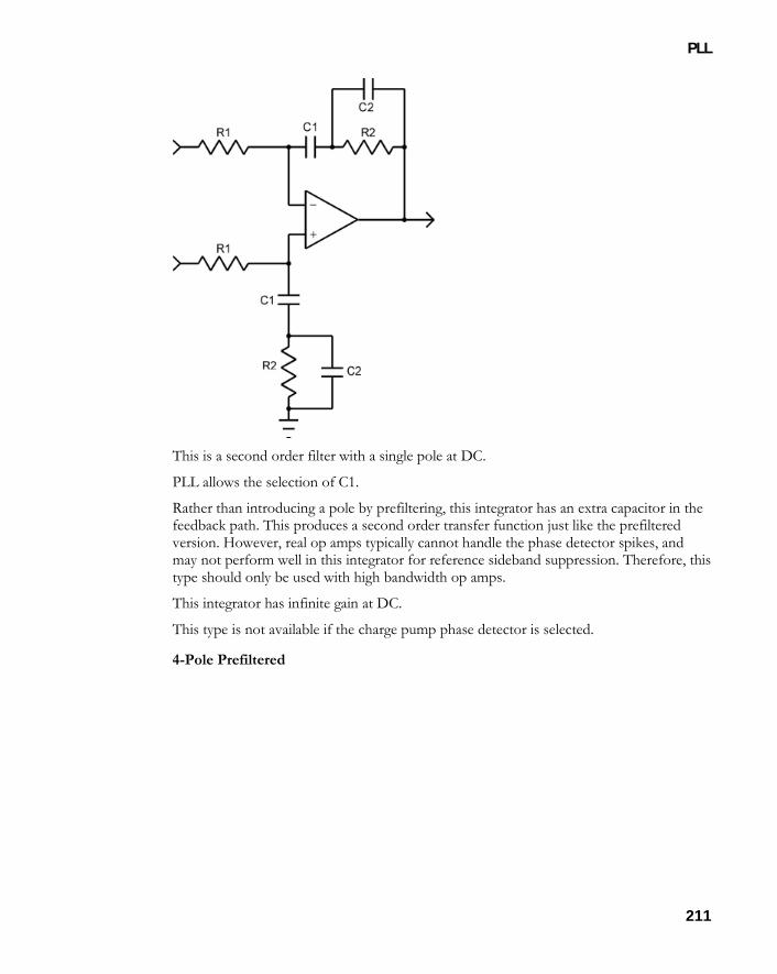
PLL
211
This is a second order filter with a single pole at DC.
PLL allows the selection of C1.
Rather than introducing a pole by prefiltering, this integrator has an extra capacitor in the feedback path. This produces a second order transfer function just like the prefiltered version. However, real op amps typically cannot handle the phase detector spikes, and may not perform well in this integrator for reference sideband suppression. Therefore, this type should only be used with high bandwidth op amps.
This integrator has infinite gain at DC.
This type is not available if the charge pump phase detector is selected.
4-Pole Prefiltered
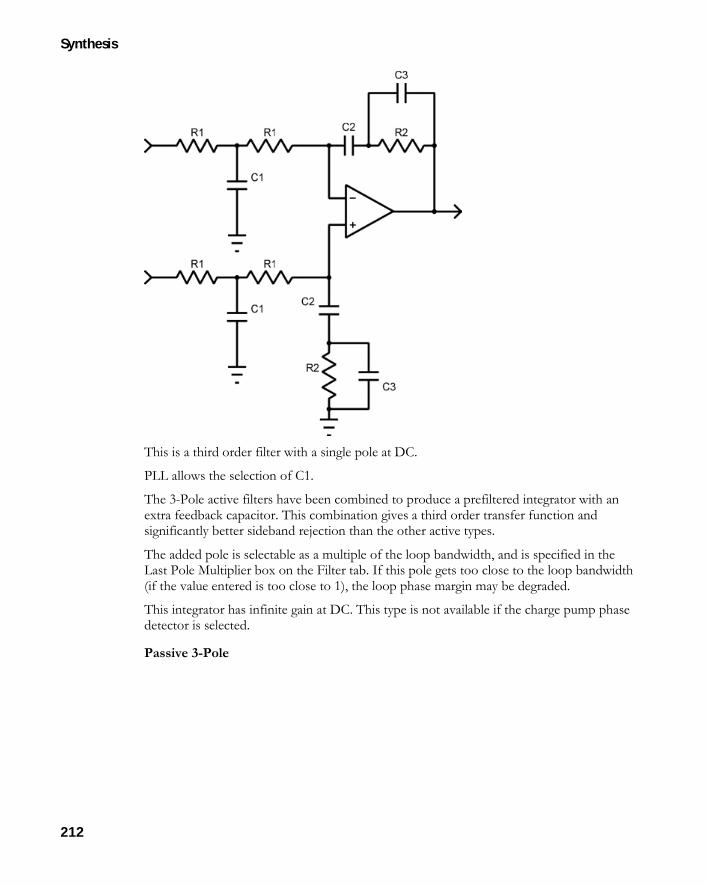
Synthesis
212
This is a third order filter with a single pole at DC.
PLL allows the selection of C1.
The 3-Pole active filters have been combined to produce a prefiltered integrator with an extra feedback capacitor. This combination gives a third order transfer function and significantly better sideband rejection than the other active types.
The added pole is selectable as a multiple of the loop bandwidth, and is specified in the Last Pole Multiplier box on the Filter tab. If this pole gets too close to the loop bandwidth (if the value entered is too close to 1), the loop phase margin may be degraded.
This integrator has infinite gain at DC. This type is not available if the charge pump phase detector is selected.
Passive 3-Pole
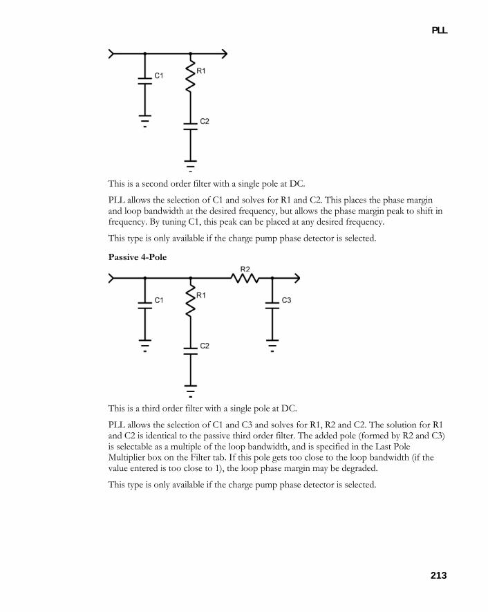
PLL
213
This is a second order filter with a single pole at DC.
PLL allows the selection of C1 and solves for R1 and C2. This places the phase margin and loop bandwidth at the desired frequency, but allows the phase margin peak to shift in frequency. By tuning C1, this peak can be placed at any desired frequency.
This type is only available if the charge pump phase detector is selected.
Passive 4-Pole
This is a third order filter with a single pole at DC.
PLL allows the selection of C1 and C3 and solves for R1, R2 and C2. The solution for R1 and C2 is identical to the passive third order filter. The added pole (formed by R2 and C3) is selectable as a multiple of the loop bandwidth, and is specified in the Last Pole Multiplier box on the Filter tab. If this pole gets too close to the loop bandwidth (if the value entered is too close to 1), the loop phase margin may be degraded.
This type is only available if the charge pump phase detector is selected.
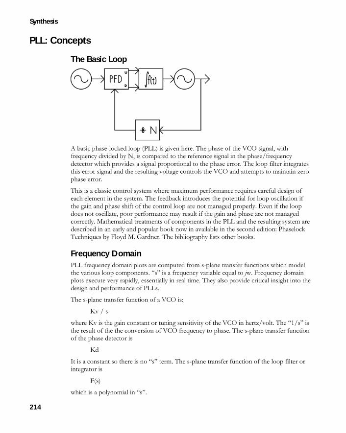
Synthesis
214
PLL: Concepts
The Basic Loop
A basic phase-locked loop (PLL) is given here. The phase of the VCO signal, with frequency divided by N, is compared to the reference signal in the phase/frequency detector which provides a signal proportional to the phase error. The loop filter integrates this error signal and the resulting voltage controls the VCO and attempts to maintain zero phase error.
This is a classic control system where maximum performance requires careful design of each element in the system. The feedback introduces the potential for loop oscillation if the gain and phase shift of the control loop are not managed properly. Even if the loop does not oscillate, poor performance may result if the gain and phase are not managed correctly. Mathematical treatments of components in the PLL and the resulting system are described in an early and popular book now in available in the second edition: Phaselock Techniques by Floyd M. Gardner. The bibliography lists other books.
Frequency Domain PLL frequency domain plots are computed from s-plane transfer functions which model the various loop components. “s” is a frequency variable equal to jw. Frequency domain plots execute very rapidly, essentially in real time. They also provide critical insight into the design and performance of PLLs.
The s-plane transfer function of a VCO is:
Kv / s
where Kv is the gain constant or tuning sensitivity of the VCO in hertz/volt. The “1/s” is the result of the the conversion of VCO frequency to phase. The s-plane transfer function of the phase detector is
Kd
It is a constant so there is no “s” term. The s-plane transfer function of the loop filter or integrator is
F(s)
which is a polynomial in “s”.
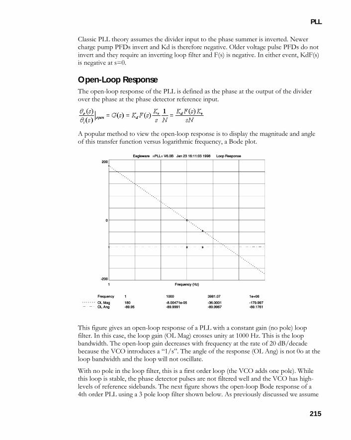
PLL
215
Classic PLL theory assumes the divider input to the phase summer is inverted. Newer charge pump PFDs invert and Kd is therefore negative. Older voltage pulse PFDs do not invert and they require an inverting loop filter and F(s) is negative. In either event, KdF(s) is negative at s=0.
Open-Loop Response The open-loop response of the PLL is defined as the phase at the output of the divider over the phase at the phase detector reference input.
A popular method to view the open-loop response is to display the magnitude and angle of this transfer function versus logarithmic frequency, a Bode plot.
This figure gives an open-loop response of a PLL with a constant gain (no pole) loop filter. In this case, the loop gain (OL Mag) crosses unity at 1000 Hz. This is the loop bandwidth. The open-loop gain decreases with frequency at the rate of 20 dB/decade because the VCO introduces a “1/s”. The angle of the response (OL Ang) is not 0o at the loop bandwidth and the loop will not oscillate.
With no pole in the loop filter, this is a first order loop (the VCO adds one pole). While this loop is stable, the phase detector pulses are not filtered well and the VCO has high-levels of reference sidebands. The next figure shows the open-loop Bode response of a 4th order PLL using a 3 pole loop filter shown below. As previously discussed we assume

Synthesis
216
the phase detector or filter inverts the divider output. Therefore, the phase margin at the 1000 Hz unity crossover frequency is 180-130°, or 50°. The magnitude of the Bode response is -17.5 dB at 4074 kHz where the angle is zero degrees. We would say the gain margin is 17.5 dB.
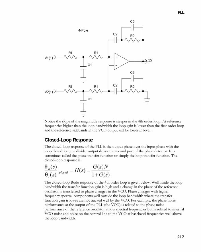
PLL
217
Notice the slope of the magnitude response is steeper in the 4th order loop. At reference frequencies higher than the loop bandwidth the loop gain is lower than the first order loop and the reference sidebands in the VCO output will be lower in level.
Closed-Loop Response The closed-loop response of the PLL is the output phase over the input phase with the loop closed, i.e., the divider output drives the second port of the phase detector. It is sometimes called the phase transfer function or simply the loop transfer function. The closed-loop response is:
The closed-loop Bode response of the 4th order loop is given below. Well inside the loop bandwidth the transfer function gain is high and a change in the phase of the reference oscillator is transferred to phase changes in the VCO. Phase changes with higher frequency spectral components well outside the loop bandwidth where the transfer function gain is lower are not tracked well by the VCO. For example, the phase noise performance at the output of the PLL (the VCO) is related to the phase noise performance of the reference oscillator at low spectral frequencies but is related to internal VCO noise and noise on the control line to the VCO at baseband frequencies well above the loop bandwidth.

Synthesis
218
Error Response This is the phase transfer function from the loop input (reference) to the phase detector output.
The error-loop response of a PLL is shown below. The error is low for spectral components within the loop bandwidth. The loop does not track spectral components of the input phase well above the loop bandwidth and the phase error at the output of the phase detector tracks the input phase.

PLL
219
Time Domain Just as the frequency domain is an important tool for the design and characterization of the PLL, the time domain is used to characterize the lock and transient behavior of the PLL.
The time domain engine in PLL operates like a system simulator. Each component in the loop is modeled as a unilateral block where the output signal is related solely to the inputs. The output of a component does not effect the input of that component. The engine starts with initial voltages of zero. For each time step, the inputs are used to calculate the outputs which then serve as future inputs. This process ripples through the network developing a time “picture” of voltages at each node. Every output is delayed by one time step from the input.
Because precise models are used in PLL for each component in the loop, the simulation characterizes the PLL more completely than analytical expressions or transforms of the frequency domain. For example, the behavior of phase/frequency detector chips is modeled at the pulse level, and, after filtering by the loop integrator, the ripples observed are actual representations of the drive to the VCO.
Because the width of phase detector pulses can be much less than the reference period, a short time step is required to accurately characterize the system. Low loop bandwidths may require significant time to lock. The combined requirement of long observation times and short time steps dictates a large number of sample points. PLL uses a number of unique methods to speed the simulation process. Models were carefully optimized for numeric efficiency. Certain components such as the reference oscillator have an output

Synthesis
220
that is independent of the input for all time steps. As a result, PLL effectively deals with simulations requiring over 100,000 steps.
The PLL we have been studying is a 1 kHz bandwidth 4th order loop. This PLL is used as a frequency synthesizer that tunes from 39 to 69 MHz in 100 kHz steps. The reference frequency is equal to the step size, 100 kHz. Therefore N varies from 390 to 690.
Integrator Output Voltage Given below is the time-domain voltage at the output of the integrator. The response first shows the initial lock process starting at t=0 with zero volts on all components. The sweep time, Tmax, is 12 ms, or 1.2 ms per division. The loop has stabilized in approximately 3.6 ms. PLL has been instructed to switch from N=390 to 450 at t=5 ms and the PLL requires approximately 2.5 ms to settle. A switch back to N=390 occurs at t=10 ms.
The non-periodic waveform trace below is the integrator output zoomed to a time span of 0.23 ms starting at 4.986 ms, just before the switch from N=390 to 450. The square waveform is the divider output and the sinusoid is the reference oscillator.

PLL
221
Prior to t=5 ms the phase of the reference and the divider output are aligned (marker 1). At t=5+ ms (marker 2) the divider output changes and the integrator output voltage begins to rise. The loop bandwidth limits the rate of change and long before the phase error is returned to zero the phase of the reference oscillator and the divider output happen to align momentarily (marker 3), even though the frequencies are unequal. This causes the integrator output to momentarily stop increasing, causing the scalloping effect during the transition to the new lock frequency, which is evident the first figure above.
Loop Order A constant VCO frequency naturally causes phase to rotate with time, introducing a pole (1/s) in the s-domain. Therefore, a loop filter with no pole (constant gain) results in a PLL with one pole, a first-order loop. This loop is not generally useful in digital PLLs because the phase detector error signal consists of pulses which when unfiltered would modulate high-level reference frequency sidebands onto the VCO.
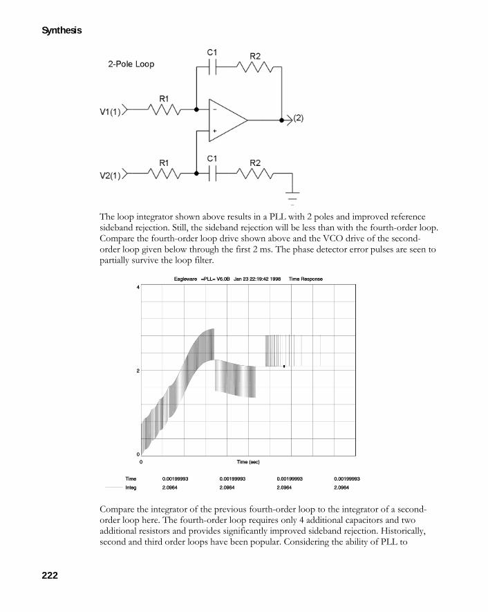
Synthesis
222
The loop integrator shown above results in a PLL with 2 poles and improved reference sideband rejection. Still, the sideband rejection will be less than with the fourth-order loop. Compare the fourth-order loop drive shown above and the VCO drive of the second-order loop given below through the first 2 ms. The phase detector error pulses are seen to partially survive the loop filter.
Compare the integrator of the previous fourth-order loop to the integrator of a second-order loop here. The fourth-order loop requires only 4 additional capacitors and two additional resistors and provides significantly improved sideband rejection. Historically, second and third order loops have been popular. Considering the ability of PLL to

PLL
223
synthesize and carefully analyze the PLL, the use of higher order loops is indicated when good sideband rejection is required.
Extra Loop Filters
Further improvement in sideband rejection is achieved by an adding a filter between the loop integrator and the VCO. The figure above shows the voltages after the integrator and after an additional third-order Butterworth lowpass filter with a cutoff of 10 kHz. The selected cutoff frequency is midway geometrically between the 1 kHz loop bandwidth and the 100 kHz reference frequency.
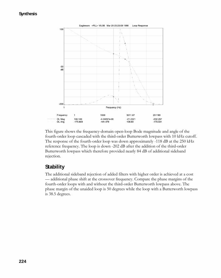
Synthesis
224
This figure shows the frequency-domain open-loop Bode magnitude and angle of the fourth-order loop cascaded with the third-order Butterworth lowpass with 10 kHz cutoff. The response of the fourth-order loop was down approximately -118 dB at the 250 kHz reference frequency. The loop is down -202 dB after the addition of the third-order Butterworth lowpass which therefore provided nearly 84 dB of additional sideband rejection.
Stability The additional sideband rejection of added filters with higher order is achieved at a cost — additional phase shift at the crossover frequency. Compare the phase margins of the fourth-order loops with and without the third-order Butterworth lowpass above. The phase margin of the unaided loop is 50 degrees while the loop with a Butterworth lowpass is 38.5 degrees.

PLL
225
How does the phase margin impact the loop stability and how is loop stability defined? The figure on the left above shows the closed-loop response of a third-order PLL with a loop bandwidth of 1000 hertz and phase margins of 30, 45, and 60 degrees. The vertical scales are 1 dB per division and the horizontal frequency scales sweep from 10 to 10000 hertz.
Reduced phase margin results in greater peaking in the closed loop response. With no phase peak the peak is infinite and oscillation results. Peaking in the closed-loop response is mimicked by peaking in the PLL error-loop and the single-sideband phase noise.
The figure on the right above shows the time-domain responses of the VCO drive which result from a step change in N of a third-order loop with phase margins of 30, 45 and 60 degrees. Lower phase margins result in ringing.
An extra loop filter introduces additional phase shift. The phase shift of a Butterworth filter at the cutoff frequency is 45 degrees times the order. For example, a third order Butterworth introduces 135 degrees of phase at the cutoff frequency but zero degrees at DC. If the cutoff frequency of the added filter is several times the loop unity gain crossover frequency (the loop bandwidth) then the additional phase may be tolerable.

Synthesis
226
Increasing the cutoff frequency of the added filter to reduce the phase shift places the cutoff nearer the reference frequency and reduces the sideband rejection. The optimum filter order and cutoff frequency placement of an added loop filter is a function of the required additional sideband rejection.
Butterworth N=1
ButterworthN=3
ButterworthN=5
Chebyshev N=5
Cauer
N=3
Cauer
N=5
Fc/FBW 3.73 7.63 12.4 13.4 6.00 11.4
10 dB 11.2 11.1 15.4 17.2 10.8 13.7
20 dB 37.1 16.4 19.6 20.2 15.0 15.3
30 dB 118 24.1 24.7 24.4 20.2 16.8
40 dB 296 35.5 31.1 29.7 25.9 18.2
50 dB 1179 52.0 39.2 36.7 30.7 19.2
60 dB 3731 76.3 49.3 45.6
70 dB 11802 112 62.0 56.9
80 dB 37313 164 78.1 71.4
90 dB 241 98.3 89.4
100 dB 354 124 112
This table gives the ratios of the reference frequency to the frequency at which the phase shift is 15° for 6 representative lowpass filter types. The row labeled Fc over FBW is the cutoff frequency normalized to the loop bandwidth, the frequency at which we wish to hold the phase shift to 15°. For example, when adding a fifth-order Butterworth filter to the loop, to hold the phase shift at the loop bandwidth to 15°, the cutoff should be 12.4 times the loop bandwidth. Specifying a higher filter cutoff frequency improves the phase margin but reduces sideband rejection.
The first column numbers are the desired additional reference sideband rejection of the filter and rows 2 through 11 are the required ratios of the reference frequency to loop bandwidth. Small ratios are desirable because for a given reference frequency a higher loop bandwidth results in fast lock times and generally improved phase noise. For example, if 30 dB of additional rejection is required, of the filters listed the fifth-order Cauer-Chebyshev allows the smallest ratio.
Notice from the row labeled 15° that if the added filter order is increased then the cutoff frequency must be increased to maintain the phase shift at the loop bandwidth to 15° or less. Also, notice for the all-pole filters that smaller ratios are not always achieved with higher order. There is an optimum order that increases with increasing sideband rejection requirements.

PLL
227
Noise
Phase Noise PLL computes the phase-locked loop SSB phase-noise utilizing techniques which consider the effects of virtually every loop component down to the resistors in the loop filter. This data is then displayed in a format which makes it easy to identify the most offensive blocks in the PLL.
The phase noise of the reference oscillator and VCO are computed from user entered parameters such as loaded Q, amplifier noise figure,etc., or the phase noise of the oscillators may be entered versus offset frequency. The phase noise of the phase detector and the divider are entered as phase-noise floors. The noise contribution of the loop filter is automatically calculated by PLL based on opamp parameters and Nyquist (thermal) noise in the resistors in the loop filter.
Oscillator Noise The noise of the reference oscillator may be entered versus offset frequency in a simple list with up to ten offset frequency points. Noise is interpolated between these frequency points. Alternatively, you may enter oscillator parameters which PLL then uses to compute SSB phase noise from Leeson’s equation. Leeson considered the oscillator as the cascade of an amplifier with a resonator in a feedback loop. The resulting relatively simple expression is an elegant method of predicting oscillator phase-noise performance. Detailed oscillator design procedures and definitions of the parameters involved are given in Oscillator Design and Computer Simulation. The single-sideband phase noise due to Leeson of an oscillator is:
where:
fo = Carrier Frequency (Hz) Ql = Loaded Q fm = Modulation, baseband, of offset frequency (Hz) fc = active device flicker corner (Hz) F = amplifier noise factor k = Boltzmann's Constant T = Temperature (Kelvin) Ps = Output power (watts)
Notice that the SSB noise performance improves with the square of the loaded Q but only linearly with decreasing amplifier noise factor. Increased output power also improves noise performance. Amazingly, since the difference in the noise factor of a typical and a state-of-the-art amplifier is only a few decibels, the amplifier noise figure is a relatively unimportant factor in oscillator noise performance. Output power and especially loaded Q are the most important factors is oscillator noise performance.

Synthesis
228
Given above is the SSB phase noise of an oscillator with fo=100MHz, Ql=500, fc=1000Hz, F=5dB, and Ps=0dBm. The resonator half-power bandwidth, fo/2Ql is 1E8/2*500 or 100kHz. Notice at this offset frequency the SSB phase noise begins to rise at the rate of 20dB per decade as the carrier frequency is approached. At offset frequencies much higher than the half-power bandwidth (marker number 4), the phase-noise is simply FkT/Ps. In decibel format this is:
L(fm)(dBc/Hz) = -177 + F(dB) - Ps(dBm)
The constant factor is -177 and not the familiar -174 because it is 1/2 kT. Half of the total noise power is in the other sideband.
At offset frequencies less than fc, the noise rises at an additional 10 dB per decade as the carrier is approached.
Divider and Phase Detector Noise The SSB phase noise contribution from the digital dividers and the phase detector are specified in PLL as noise floors in dBc/Hz.
Crawford has collected phase-noise data from a number of sources for digital dividers. There is some disagreement within the data but the following approximations serve as a starting point. In general the noise is relatively flat at offset frequencies greater than 1 kHz and rises at less than 10 dB per decade closer to the carrier. Above 1 kHz typical values range from -145 to -165 dBc/Hz for silicon devices and 20 dB worse for GaAs devices. The inferior performance of GaAs devices decreases at offset frequencies greater than 100 kHz.

PLL
229
The noise floor of modern phase/frequency detectors and charge-pumps is typically in the range of -150 to -157 dBc/Hz. The noise floor of double-balanced mixers is superior, typically -170 to -180 dBc/Hz. Unfortunately these phase detectors do not have the locking and tracking range of the phase/frequency detectors.
Loop Filter (Integrator) Noise Noise from the loop filter includes contributions from thermally induced noise voltage in each resistor and from noise sources in the operational amplifier.
The rms thermal noise voltage generated in one Hertz bandwidth in a resistor (Nyquist noise) is:
Vn = sqrt(4kTR)
Even the resistor in the passive filter following a charge-pump phase detector can have a profound impact on the noise performance of the PLL, particularly for large values of R. When an active loop filter is used, each of the resistors contributes to the overall PLL noise. The voltage developed in each resistor is multiplied by the transfer function from that resistor to the VCO drive voltage. In addition, the input noise voltage and noise current of the opamp are transferred to noise modulation on the VCO. PLL automatically computes these contributions.
Loop Action on the Total Noise
Shown above are the total PLL SSB phase noise, the contribution to this noise of the VCO and the contribution to the total noise from a divider noise floor of -157 dBc/Hz. This example uses the 100 MHz VCO, a divider N=100, and a passive 3rd-order loop
Synthesis
230
filter. The divider noise floor of -157 dBc/Hz is referred to the phase detector with a reference frequency of 1 MHz. The phase noise contribution at the PLL output at 100 MHz is 20log(N) worse, -157 dBc/Hz + 40 dB = -117 dBc/Hz. The VCO phase noise is -117 dBc/Hz at approximately 350 Hz. The PLL was designed with a loop bandwidth equal to 350 Hz. This is a general guideline for “optimum” phase noise performance. However, a lower loop bandwidth will generally improve phase-noise at offsets higher than the loop bandwidth and a higher loop bandwidth will improve the phase noise near and inside the loop bandwidth.
The top dashed trace above is the total PLL SSB phase noise. For illustration, all contributions to PLL noise except the VCO and divider have been eliminated.
The solid trace above is the VCO contribution to the total PLL phase noise. Notice that the action of the loop has been to effectively decrease the phase noise from the VCO inside the loop bandwidth. The original VCO phase noise response is effectively multiplied by the PLL closed error-loop response.
The dash-dot-dot trace above is the divider phase noise floor contribution to the total PLL phase noise. Well inside the loop bandwidth it becomes the dominant noise source. Were it not for the action of the PLL this trace would be flat at -117 dBc/Hz. Well outside the loop bandwidth, the loop is unable to modulate this noise onto the VCO and it’s contribution decreases. At high offset frequencies, the VCO becomes the dominant noise source. The divider and VCO noise sources are uncorrelated and they combine on a power basis. A degradation of 3.01 dB results from equal noise sources such as at marker 2. Notice peaking in the PLL phase noise contribution from the divider. This is a related to peaking in the closed and error loops. Excessive phase noise peaking is an indication of marginal loop stability.
Overall PLL Noise
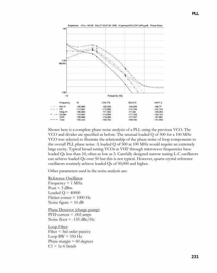
PLL
231
Shown here is a complete phase noise analysis of a PLL using the previous VCO. The VCO and divider are specified as before. The unusual loaded Q of 500 for a 100 MHz VCO was selected to illustrate the relationship of the phase noise of loop components to the overall PLL phase noise. A loaded Q of 500 at 100 MHz would require an extremely large cavity. Typical broad tuning VCOs at VHF through microwave frequencies have loaded Qs less than 10, often as low as 3. Carefully designed narrow tuning L-C oscillators can achieve loaded Qs over 50 but this is not typical. However, quartz crystal reference oscillators routinely achieve loaded Qs of 50,000 and higher.
Other parameters used in the noise analysis are:
Reference Oscillator: Frequency = 1 MHz Pout = 3 dBm Loaded Q = 40000 Flicker corner = 1000 Hz Noise figure = 10 dB
Phase Detector (charge-pump): PFD current = .002 amps Noise floor = -155 dBc/Hz
Loop Filter: Filter = 3rd order passive Loop BW = 350 Hz Phase margin = 60 degrees C1 = 1e-6 farads

Synthesis
232
R1 = 30.6 ohms C2 = 3e-5 farads
At 10 Hz offset the primary source of PLL phase noise is the reference oscillator. At approximately 50 Hz, the reference, phase detector and divider are equal contributors to a total SSB phase noise of -110 dBc/Hz. At higher offset frequencies the primary contributor is the integrator. Because this example uses a passive 3rd-order loop, this is Nyquist noise in R1.
At offset frequencies above 30 kHz the primary contributor is the VCO. Because integrator, phase detector and divider noise are introduced through the VCO drive voltage, an additional filter after the loop integrator could be used to reduce the phase noise. Remember, to maintain loop stability and additional loop filter must have a cutoff significantly higher than the loop bandwidth. Also, this additional loop filter will not reduce the phase noise at offset frequencies where VCO noise dominates.
Given below is the SSB phase noise performance of the previous PLL with a 0.1 dB passband ripple, 26 dB Amin, 3rd-order elliptic lowpass with a cutoff frequency of 2.1 kHz. This filter substantially reduces integrator, phase detector and divider noise above approximately 3 kHzso that the VCO limits the SSB phase noise performance.
Residual FM and PM Noise If an unmodulated oscillator is phase demodulated the resulting output voltage is the residual phase modulation resulting from phase noise on the carrier. It is sometimes referred to as incidental phase modulation. The demodulated baseband signal is important only over a limited frequency range. For example, typical baseband frequencies for voice

PLL
233
communications are 50 to 3000 Hz, for Doppler radar are 1 Hz to 10 MHz and for navigation systems are subhertz to 10 Hz.
Residual PM may be found by integrating the SSB phase noise over the baseband frequency range of interest. The square of the rms residual PM is
Likewise, for rms residual FM
Residual PM and FM are related to the ultimate system S/N. If the desired signal rms deviation is , then
Besides relating directly to system performance, residual PM and FM are easier to measure than SSB phase noise, using less expensive instruments. So why is is oscillator and PLL phase noise typically specified as the SSB phase noise? Because the residuals can be found from the SSB phase noise but the inverse is not true without assuming a slope of the SSB phase noise versus offset frequency.
PLL computes rms residual PM and FM by integrating the SSB phase noise over the baseband frequency range specified in the SIM tab. The results are given in the report output section.
Loop Types
Frequency Synthesizer This loop type is simply a frequency multiplier, since its output frequency is equal the reference frequency multiplied by N. It is also the basis for all the other loop types that PLL designs.
In a frequency synthesizer PLL, the VCO output is divided by N, and compared with the reference frequency. By changing N, the VCO frequency can be set at any desired multiple of the reference, thereby “synthesizing” a desired output. In multi-channel applications, the loop is designed with a selectable N, which allows the loop to lock onto a new channel by simply changing N.
For multi-channel applications:
• The reference frequency should be chosen equal to the desired channel spacing. For example, in a 88-108 MHz FM synthesizer loop, the reference frequency should be 100 kHz (the station allocations are every 200 kHz, but occur at odd

Synthesis
234
multiples of 100 kHz). In this case, N should vary from 880 to 1080 to give the necessary tuning range.
• The Divider N prompt in the PD/÷ tab should be chosen mid way between the desired minimum and maximum. For the FM synthesizer mentioned above, this prompt should be chosen around 980.
Frequency Modulator A frequency modulator is formed by summing a voltage at the VCO input. This directly modulates the VCO, producing a FM characteristic at the PLL output frequency.
For multi-channel applications:
• The reference frequency should be chosen equal to the desired channel spacing. For example, in a 88-108 MHz FM synthesizer loop, the reference frequency should be 100 kHz (the station allocations are every 200 kHz, but occur at odd multiples of 100 kHz). In this case, N should vary from 880 to 1080 to give the necessary tuning range.
• The Divider N prompt in the PD/÷ tab should be chosen mid way between the desired minimum and maximum. For the FM synthesizer mentioned above, this prompt should be chosen around 980.
Note: N can be chosen at some value other than the mid-range, but be aware that loop stability is hard to maintain with large variations in N.
• The lowest modulating signal frequency must be higher than the loop bandwidth to keep the loop from correcting the desired frequency error.
• The amplitude of the modulating signal determines the VCO frequency swing. However, the signal amplitude must be small enough that the loop can maintain lock during the modulation. This maximum amplitude is determined entirely by the loop design, and may take some simulation to determine.
Frequency Demodulator Frequency demodulator loops take a modulated reference signal and produce an output which is proportional to the reference frequency deviation.
This type of loop is formed by taking the output from the VCO input.
Design Tips:
• The highest signal frequency which modulates the reference should be lower than the loop bandwidth since the integrator provides a lowpass filtering effect.
• The VCO output is usually not of interest in this type of loop. To reduce overall phase noise, the divider can be completely removed, or the loop can be designed with a small N.
Phase Modulator

PLL
235
A phase modulator loop can be formed in two ways:
1. By summing a voltage at the phase detector output.
2. By summing the derivative of a modulation signal at the VCO input.
PLL uses the second approach since differential phase detectors preclude summing a single voltage at the detector output without adding complexity.
The differentiator used in PLL is a first order LC highpass filter with its cutoff at the loop bandwidth.
Design Tips:
• To keep the loop from correcting the desired phase error, the lowest modulation signal frequency must be higher than the loop bandwidth.
• When selecting the modulation signal frequency, the higher the better. However, this frequency must be lower than the VCO RC bandwidth. Otherwise, the VCO will behave like a lowpass filter, and attenuate the modulating signal.
Note: The VCO bandwidth can be overcome to a small degree by increasing the modulating signal’s amplitude, but be aware that most loops may not be able to acquire or maintain lock for large signal swings at the VCO input.
Phase Demodulator Phase demodulator loops take a modulated reference signal and produce an output which is proportional to the reference phase deviation.
A phase demodulator loop can be formed in two ways:
1. By taking a voltage at the phase detector output.
2. By taking the integral of the VCO input.
PLL uses the first approach. When the Phase/Frequency Detector is used, PLL inserts a differential amplifier to produce a single output voltage from the dual outputs.
Design Tips:
• To prevent the loop from correcting the desired phase error, the lowest signal frequency which modulates the reference should be higher than the loop bandwidth.
• The VCO output is usually not of interest in this type of loop. To reduce overall phase noise, the divider can be completely removed, or the loop can be designed with a small N.

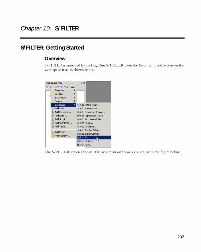
237
Chapter 10: S/FILTER
S/FILTER: Getting Started
Overview S/FILTER is launched by clicking Run S/FILTER from the New Item tool button on the workspace tree, as shown below.
The S/FILTER screen appears. The screen should now look similar to the figure below:
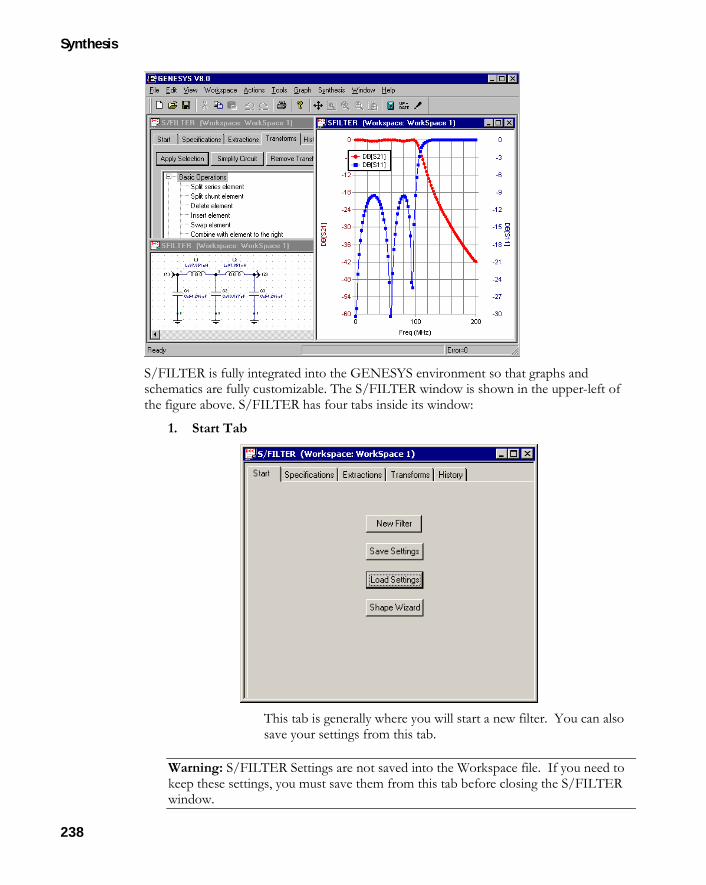
Synthesis
238
S/FILTER is fully integrated into the GENESYS environment so that graphs and schematics are fully customizable. The S/FILTER window is shown in the upper-left of the figure above. S/FILTER has four tabs inside its window:
1. Start Tab
This tab is generally where you will start a new filter. You can also save your settings from this tab.
Warning: S/FILTER Settings are not saved into the Workspace file. If you need to keep these settings, you must save them from this tab before closing the S/FILTER window.

S/FILTER
239
2. Specifications Tab
Initial electrical design parameters are entered into this tab, such as cutoff frequencies and transmission zero locations.
3. Extractions Tab
Physical realization parameters are entered in this tab, such as desired element values. S/FILTER fills in the table with solutions fitting the desired electrical criteria from the Design Tab, and (if specified) the physical criteria from the Extractions Tab.
4. Transforms Tab
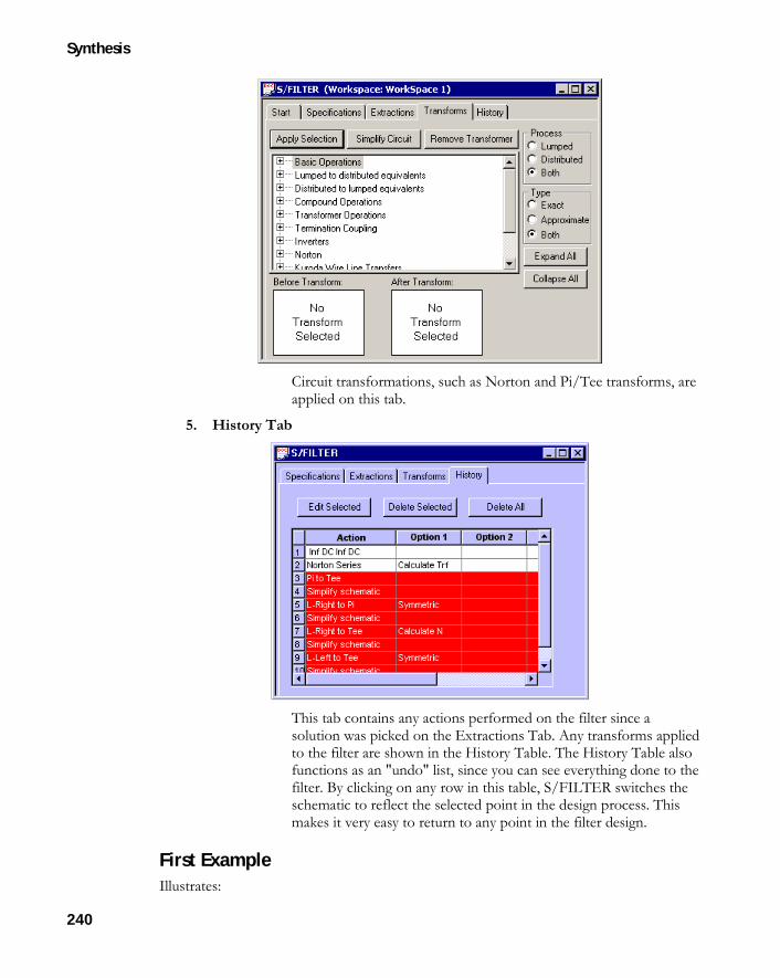
Synthesis
240
Circuit transformations, such as Norton and Pi/Tee transforms, are applied on this tab.
5. History Tab
This tab contains any actions performed on the filter since a solution was picked on the Extractions Tab. Any transforms applied to the filter are shown in the History Table. The History Table also functions as an "undo" list, since you can see everything done to the filter. By clicking on any row in this table, S/FILTER switches the schematic to reflect the selected point in the design process. This makes it very easy to return to any point in the filter design.
First Example Illustrates:
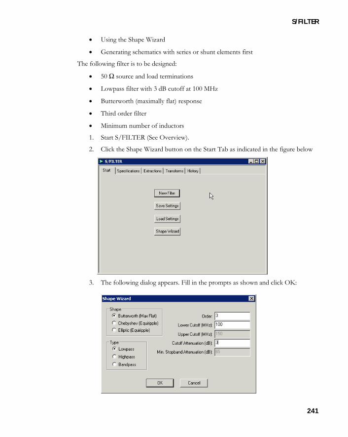
S/FILTER
241
• Using the Shape Wizard
• Generating schematics with series or shunt elements first
The following filter is to be designed:
• 50 Ω source and load terminations
• Lowpass filter with 3 dB cutoff at 100 MHz
• Butterworth (maximally flat) response
• Third order filter
• Minimum number of inductors
1. Start S/FILTER (See Overview).
2. Click the Shape Wizard button on the Start Tab as indicated in the figure below
3. The following dialog appears. Fill in the prompts as shown and click OK:

Synthesis
242
4. Enter '50' into the Source and Load boxes on the Specifications Tab. This sets the terminations to 50 Ω each.
5. This tool is used when a classic response shape is needed. The S/FILTER specifications tab should now look like the figure below.
Notice that the Shape Wizard has filled in several prompts. The Cutoff frequency has been set to 100 MHz, as requested. The filter type has been set to lowpass, and the shape has been set to maximally flat.
The Zero Table contains information on the order of the filter. The DC row has been disabled because by definition, lowpass filters cannot have a transmission zero at DC. Since Butterworth filters are all-pole, there are no finite zeros defined in the grid; only zeros at infinity. The three zeros at infinity make this a third order filter.
The response for this filter is shown below. If your response is scaled differently, click the Rescale Plot button on the Specifications Tab.
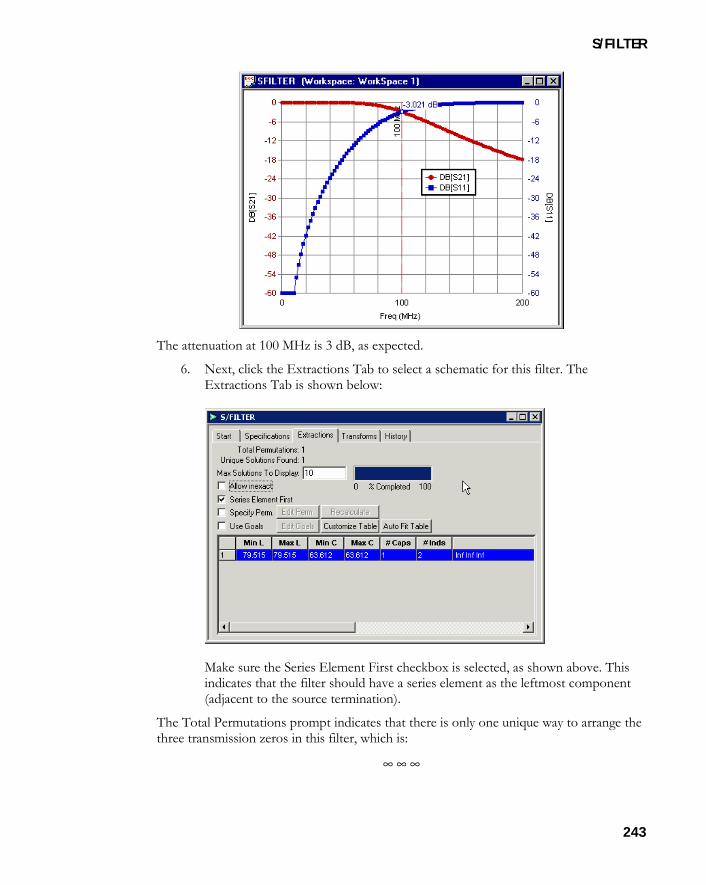
S/FILTER
243
The attenuation at 100 MHz is 3 dB, as expected.
6. Next, click the Extractions Tab to select a schematic for this filter. The Extractions Tab is shown below:
Make sure the Series Element First checkbox is selected, as shown above. This indicates that the filter should have a series element as the leftmost component (adjacent to the source termination).
The Total Permutations prompt indicates that there is only one unique way to arrange the three transmission zeros in this filter, which is:
∞ ∞ ∞
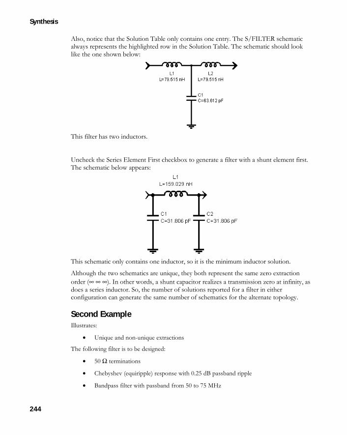
Synthesis
244
Also, notice that the Solution Table only contains one entry. The S/FILTER schematic always represents the highlighted row in the Solution Table. The schematic should look like the one shown below:
This filter has two inductors.
Uncheck the Series Element First checkbox to generate a filter with a shunt element first. The schematic below appears:
This schematic only contains one inductor, so it is the minimum inductor solution.
Although the two schematics are unique, they both represent the same zero extraction order (∞ ∞ ∞). In other words, a shunt capacitor realizes a transmission zero at infinity, as does a series inductor. So, the number of solutions reported for a filter in either configuration can generate the same number of schematics for the alternate topology.
Second Example Illustrates:
• Unique and non-unique extractions
The following filter is to be designed:
• 50 Ω terminations
• Chebyshev (equiripple) response with 0.25 dB passband ripple
• Bandpass filter with passband from 50 to 75 MHz
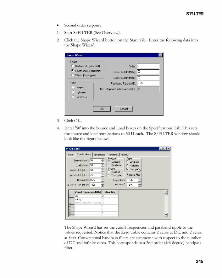
S/FILTER
245
• Second order response
1. Start S/FILTER (See Overview).
2. Click the Shape Wizard button on the Start Tab. Enter the following data into the Shape Wizard:
3. Click OK.
4. Enter '50' into the Source and Load boxes on the Specifications Tab. This sets the source and load terminations to 50 Ω each. The S/FILTER window should look like the figure below:
The Shape Wizard has set the cutoff frequencies and passband ripple to the values requested. Notice that the Zero Table contains 2 zeros at DC, and 2 zeros at f=∞. Conventional bandpass filters are symmetric with respect to the number of DC and infinite zeros. This corresponds to a 2nd order (4th degree) bandpass filter.
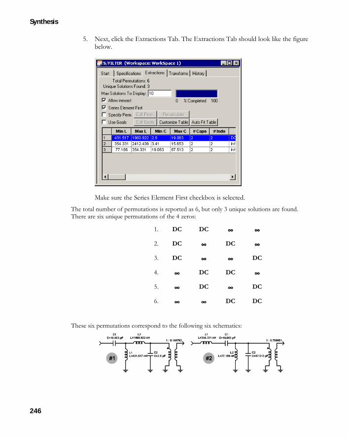
Synthesis
246
5. Next, click the Extractions Tab. The Extractions Tab should look like the figure below.
Make sure the Series Element First checkbox is selected.
The total number of permutations is reported as 6, but only 3 unique solutions are found. There are six unique permutations of the 4 zeros:
1. DC DC ∞∞∞∞ ∞∞∞∞
2. DC ∞∞∞∞ DC ∞∞∞∞
3. DC ∞∞∞∞ ∞∞∞∞ DC
4. ∞∞∞∞ DC DC ∞∞∞∞
5. ∞∞∞∞ DC ∞∞∞∞ DC
6. ∞∞∞∞ ∞∞∞∞ DC DC
These six permutations correspond to the following six schematics:

S/FILTER
247
Note: If the "Series Element First" option is unselected, six more schematics are generated for the six transmission zero permutations shown above, each schematic having a shunt element adjacent to the source.
Notice that schematic #2 and schematic #3 are nearly identical, except for the series resonator element ordering. Electrically speaking, these two schematics are identical since simply changing the resonator element order does not change either the resonant frequency or the impedance presented to surrounding elements. Also, notice that schematic #4 and schematic #5 are identical to #2. Therefore, only schematics 1, 2, and 6 are unique. S/FILTER automatically detects these redundant solutions, and only includes 1 occurrence in the Solution Table.
See the Filter Design Concepts section for a discussion of extraction theory.
Third Example Illustrates:
• Finite Zeros
The following filter is to be designed:
• 50 Ω terminations
• Equiripple response with 0.1 dB passband ripple
• Bandpass filter with passband from 100 to 150 MHz
• Insertion loss greater than 30 dB below 75 MHz and above 200 MHz
Enter the following data into the Specifications Tab:
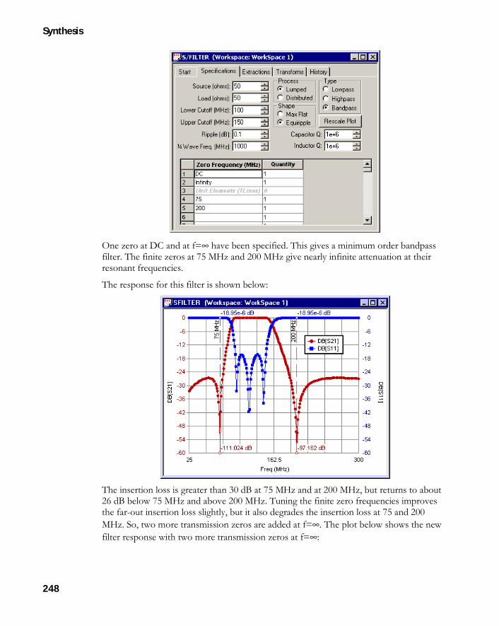
Synthesis
248
One zero at DC and at f=∞ have been specified. This gives a minimum order bandpass filter. The finite zeros at 75 MHz and 200 MHz give nearly infinite attenuation at their resonant frequencies.
The response for this filter is shown below:
The insertion loss is greater than 30 dB at 75 MHz and at 200 MHz, but returns to about 26 dB below 75 MHz and above 200 MHz. Tuning the finite zero frequencies improves the far-out insertion loss slightly, but it also degrades the insertion loss at 75 and 200 MHz. So, two more transmission zeros are added at f=∞. The plot below shows the new filter response with two more transmission zeros at f=∞:
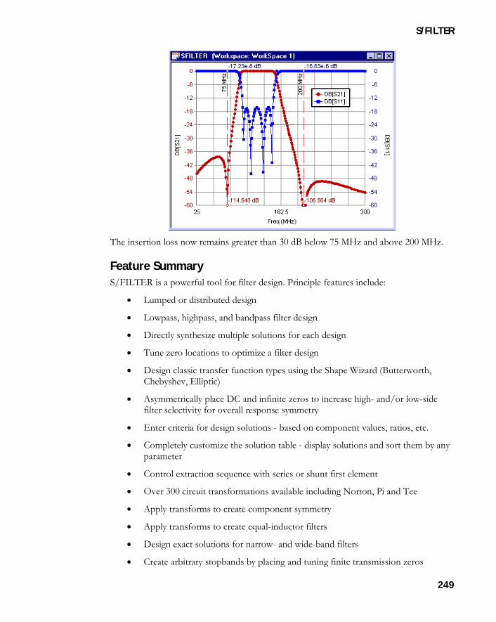
S/FILTER
249
The insertion loss now remains greater than 30 dB below 75 MHz and above 200 MHz.
Feature Summary S/FILTER is a powerful tool for filter design. Principle features include:
• Lumped or distributed design
• Lowpass, highpass, and bandpass filter design
• Directly synthesize multiple solutions for each design
• Tune zero locations to optimize a filter design
• Design classic transfer function types using the Shape Wizard (Butterworth, Chebyshev, Elliptic)
• Asymmetrically place DC and infinite zeros to increase high- and/or low-side filter selectivity for overall response symmetry
• Enter criteria for design solutions - based on component values, ratios, etc.
• Completely customize the solution table - display solutions and sort them by any parameter
• Control extraction sequence with series or shunt first element
• Over 300 circuit transformations available including Norton, Pi and Tee
• Apply transforms to create component symmetry
• Apply transforms to create equal-inductor filters
• Design exact solutions for narrow- and wide-band filters
• Create arbitrary stopbands by placing and tuning finite transmission zeros
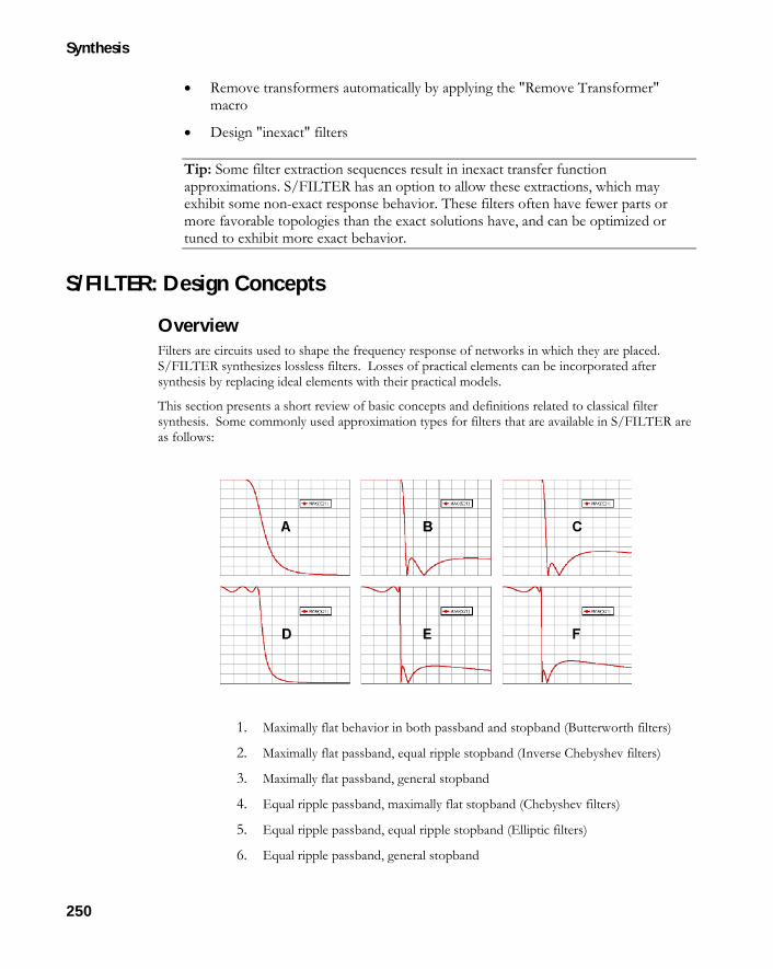
Synthesis
250
• Remove transformers automatically by applying the "Remove Transformer" macro
• Design "inexact" filters
Tip: Some filter extraction sequences result in inexact transfer function approximations. S/FILTER has an option to allow these extractions, which may exhibit some non-exact response behavior. These filters often have fewer parts or more favorable topologies than the exact solutions have, and can be optimized or tuned to exhibit more exact behavior.
S/FILTER: Design Concepts
Overview Filters are circuits used to shape the frequency response of networks in which they are placed. S/FILTER synthesizes lossless filters. Losses of practical elements can be incorporated after synthesis by replacing ideal elements with their practical models. This section presents a short review of basic concepts and definitions related to classical filter synthesis. Some commonly used approximation types for filters that are available in S/FILTER are as follows:
1. Maximally flat behavior in both passband and stopband (Butterworth filters)
2. Maximally flat passband, equal ripple stopband (Inverse Chebyshev filters)
3. Maximally flat passband, general stopband
4. Equal ripple passband, maximally flat stopband (Chebyshev filters)
5. Equal ripple passband, equal ripple stopband (Elliptic filters)
6. Equal ripple passband, general stopband
S/FILTER
251
Transmission Zeros Transmission zeros are critical frequencies where signal transmission between input and output is stopped. S/FILTER uses the transmission zero frequencies together with the passband edge frequencies and passband ripple to form the transfer function between the input and output of the filter, and for shaping the response of the filter. Transmission zeros must always be placed in the stopband(s) of a filter. Placement of transmission zeros into passbands is automatically prevented by S/FILTER.
The following transmission zero types are available:
• Transmission Zero at DC
A transmission zero at f=0 (DC) adds one degree to the filter transfer function. These transmission zeros are needed in highpass and bandpass filters. Increasing the number of transmission zeros at DC increases the selectivity (slope) of the filter in the lower stopband more than it increases the upper stopband selectivity.
• Transmission Zero at Infinity
A transmission zero at f=∞ adds one degree to the filter transfer function. These transmission zeros are needed in lowpass and bandpass filters. Increasing the number of transmission zeros at f=∞ increases the selectivity of upper stopband more than it increases the lower stopband selectivity.
• Transmission Zero at Finite Frequency
A finite-frequency transmission zero adds two degrees to the filter transfer function. During extraction, finite transmission zeros are realized either as parallel resonators in series or series resonators to ground. The parallel resonator in series stops signal flow by being an open circuit at the resonant frequency while the series resonator to ground becomes a short circuit at the resonant frequency.
Unit Elements All distributed filters exhibit a behavior called reentry. Since transmission line elements have a periodic impedance function, multiple passbands and stopbands always appear. In ideal lossless filters, each passband is identical, and these "mirror" passbands continue all the way to infinite frequency.
The response below illustrates the effect of reentry on a 1 GHz bandpass filter:
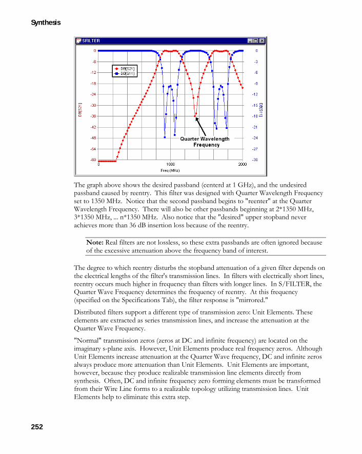
Synthesis
252
The graph above shows the desired passband (centerd at 1 GHz), and the undesired passband caused by reentry. This filter was designed with Quarter Wavelength Frequency set to 1350 MHz. Notice that the second passband begins to "reenter" at the Quarter Wavelength Frequency. There will also be other passbands beginning at 2*1350 MHz, 3*1350 MHz, ... n*1350 MHz. Also notice that the "desired" upper stopband never achieves more than 36 dB insertion loss because of the reentry.
Note: Real filters are not lossless, so these extra passbands are often ignored because of the excessive attenuation above the frequency band of interest.
The degree to which reentry disturbs the stopband attenuation of a given filter depends on the electrical lengths of the filter's transmission lines. In filters with electrically short lines, reentry occurs much higher in frequency than filters with longer lines. In S/FILTER, the Quarter Wave Frequency determines the frequency of reentry. At this frequency (specified on the Specifications Tab), the filter response is "mirrored."
Distributed filters support a different type of transmission zero: Unit Elements. These elements are extracted as series transmission lines, and increase the attenuation at the Quarter Wave Frequency.
"Normal" transmission zeros (zeros at DC and infinite frequency) are located on the imaginary s-plane axis. However, Unit Elements produce real frequency zeros. Although Unit Elements increase attenuation at the Quarter Wave frequency, DC and infinite zeros always produce more attenuation than Unit Elements. Unit Elements are important, however, because they produce realizable transmission line elements directly from synthesis. Often, DC and infinite frequency zero forming elements must be transformed from their Wire Line forms to a realizable topology utilizing transmission lines. Unit Elements help to eliminate this extra step.

S/FILTER
253
The response below shows a comparison of a 900 MHz lowpass filter designed with 3 transmission zeros at infinity, and the same filter designed with only unit elements. Notice the difference in attenuation for the two responses.
The filters below were used to generate the response above:
Filter using transmission zeros at infinity:
Filter using only Unit Elements:
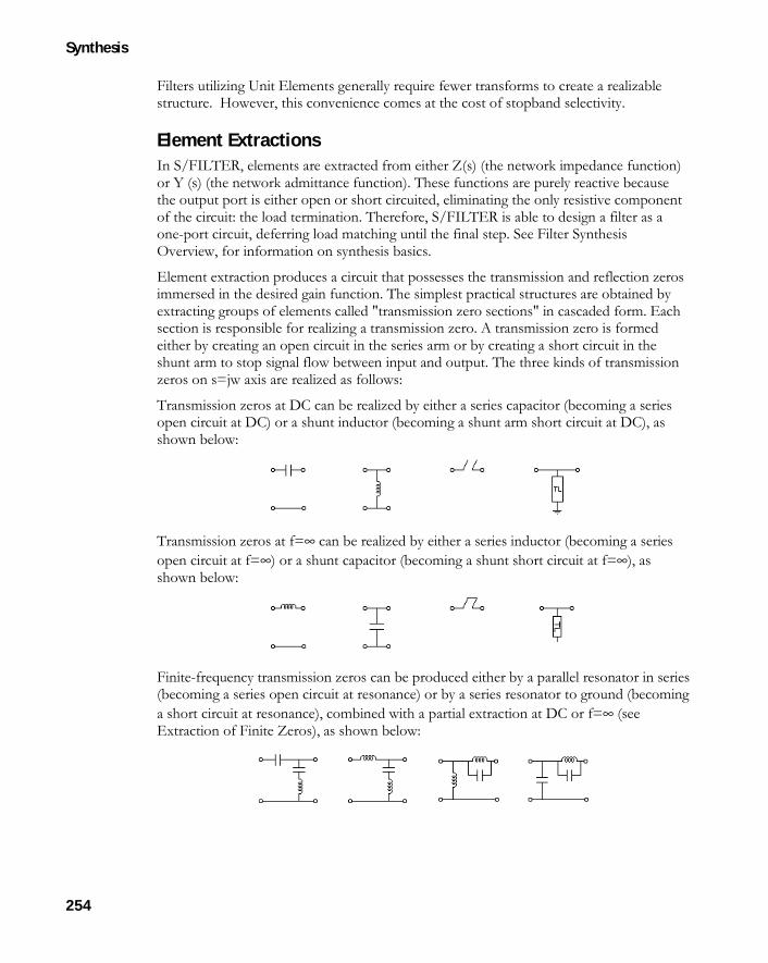
Synthesis
254
Filters utilizing Unit Elements generally require fewer transforms to create a realizable structure. However, this convenience comes at the cost of stopband selectivity.
Element Extractions In S/FILTER, elements are extracted from either Z(s) (the network impedance function) or Y (s) (the network admittance function). These functions are purely reactive because the output port is either open or short circuited, eliminating the only resistive component of the circuit: the load termination. Therefore, S/FILTER is able to design a filter as a one-port circuit, deferring load matching until the final step. See Filter Synthesis Overview, for information on synthesis basics.
Element extraction produces a circuit that possesses the transmission and reflection zeros immersed in the desired gain function. The simplest practical structures are obtained by extracting groups of elements called "transmission zero sections" in cascaded form. Each section is responsible for realizing a transmission zero. A transmission zero is formed either by creating an open circuit in the series arm or by creating a short circuit in the shunt arm to stop signal flow between input and output. The three kinds of transmission zeros on s=jw axis are realized as follows:
Transmission zeros at DC can be realized by either a series capacitor (becoming a series open circuit at DC) or a shunt inductor (becoming a shunt arm short circuit at DC), as shown below:
Transmission zeros at f=∞ can be realized by either a series inductor (becoming a series open circuit at f=∞) or a shunt capacitor (becoming a shunt short circuit at f=∞), as shown below:
Finite-frequency transmission zeros can be produced either by a parallel resonator in series (becoming a series open circuit at resonance) or by a series resonator to ground (becoming a short circuit at resonance), combined with a partial extraction at DC or f=∞ (see Extraction of Finite Zeros), as shown below:
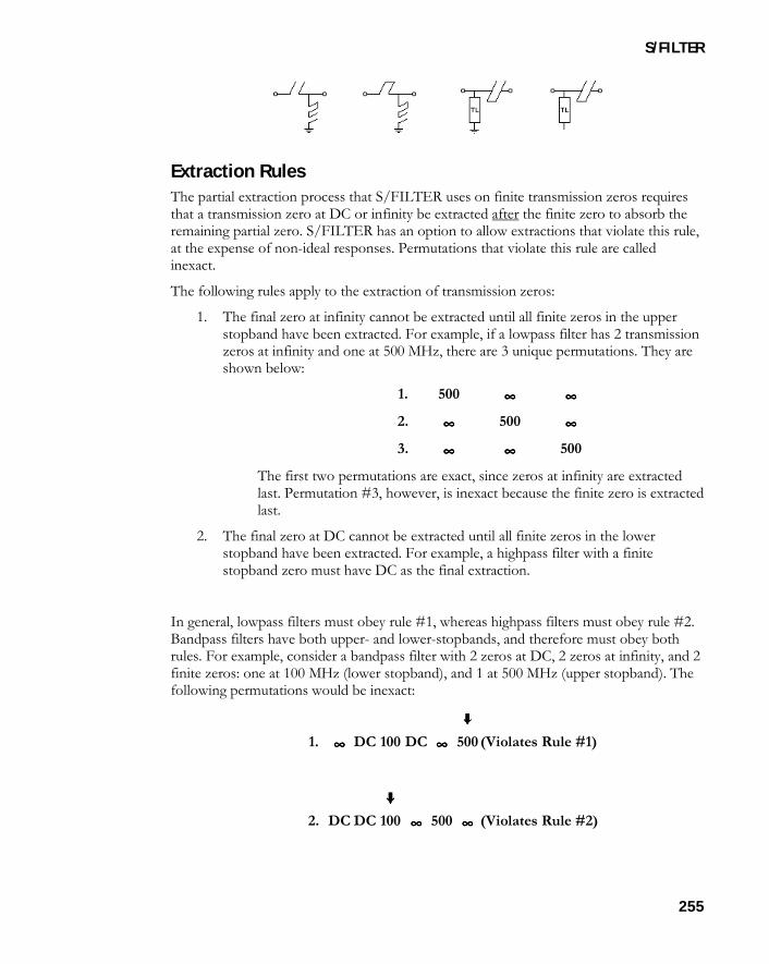
S/FILTER
255
Extraction Rules The partial extraction process that S/FILTER uses on finite transmission zeros requires that a transmission zero at DC or infinity be extracted after the finite zero to absorb the remaining partial zero. S/FILTER has an option to allow extractions that violate this rule, at the expense of non-ideal responses. Permutations that violate this rule are called inexact.
The following rules apply to the extraction of transmission zeros:
1. The final zero at infinity cannot be extracted until all finite zeros in the upper stopband have been extracted. For example, if a lowpass filter has 2 transmission zeros at infinity and one at 500 MHz, there are 3 unique permutations. They are shown below:
1. 500 ∞∞∞∞ ∞∞∞∞
2. ∞∞∞∞ 500 ∞∞∞∞
3. ∞∞∞∞ ∞∞∞∞ 500
The first two permutations are exact, since zeros at infinity are extracted last. Permutation #3, however, is inexact because the finite zero is extracted last.
2. The final zero at DC cannot be extracted until all finite zeros in the lower stopband have been extracted. For example, a highpass filter with a finite stopband zero must have DC as the final extraction.
In general, lowpass filters must obey rule #1, whereas highpass filters must obey rule #2. Bandpass filters have both upper- and lower-stopbands, and therefore must obey both rules. For example, consider a bandpass filter with 2 zeros at DC, 2 zeros at infinity, and 2 finite zeros: one at 100 MHz (lower stopband), and 1 at 500 MHz (upper stopband). The following permutations would be inexact:
1. ∞∞∞∞ DC 100 DC ∞∞∞∞ 500 (Violates Rule #1)
2. DC DC 100 ∞∞∞∞ 500 ∞∞∞∞ (Violates Rule #2)
Synthesis
256
3. ∞∞∞∞ DC ∞∞∞∞ 500 DC 100 (Violates Both Rules)
4. 100 ∞∞∞∞ DC ∞∞∞∞ 500 DC(Violates Rule #1)
5. 500 DC DC 100 ∞∞∞∞ ∞∞∞∞ (Violates Rule #2)
6. DC ∞∞∞∞ ∞∞∞∞ DC 500 100 (Violates Both Rules)
If an extraction sequence violates either of these rules, it is considered inexact since it does not exactly represent the intended transfer function. The severity of the response distortion is related to where (what position) in the extraction sequence a rule is violated. If it occurs at the last zero extraction, as in example #1 in the table above, the partial extraction only affects the last elements extracted, and usually has a minimal impact on the filter response. However, if the violation occurs early in the extraction sequence, as in example #2 in the table above, impedance differences will ripple from the first violation to the end of the structure. In most cases, this results in a poor filter response, which often requires tuning or optimization.
Note: For extraction purposes, Unit Elements are not considered to be transmission zeros, and do not modify the extraction rules given above.
Extraction Examples In the examples below, elements are labeled with the type of transmission zero they represent, rather than actual values. The number of unique permutations given in each example is valid for both lumped and distributed filters.
Example 1
200 - 250 MHz bandpass filter
2 Zeros at DC
2 Zeros at Infinity
There are 3 unique permutations with a series element first:
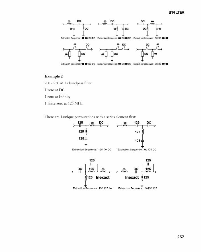
S/FILTER
257
Example 2
200 - 250 MHz bandpass filter
1 zero at DC
1 zero at Infinity
1 finite zero at 125 MHz
There are 4 unique permutations with a series element first:
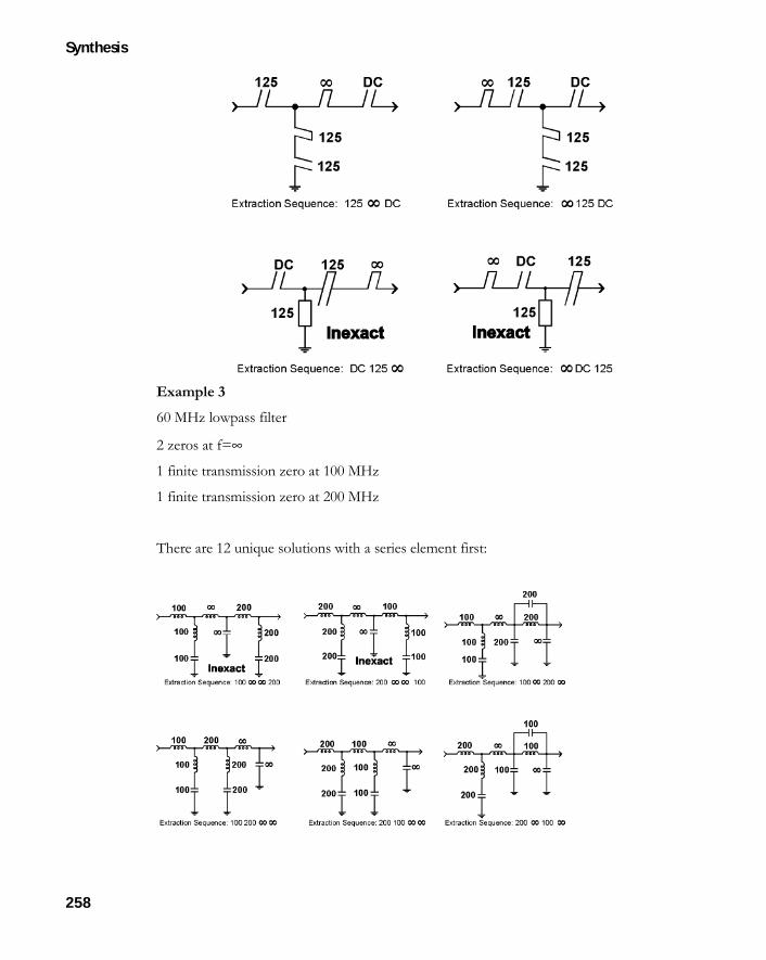
Synthesis
258
Example 3
60 MHz lowpass filter
2 zeros at f=∞
1 finite transmission zero at 100 MHz
1 finite transmission zero at 200 MHz
There are 12 unique solutions with a series element first:
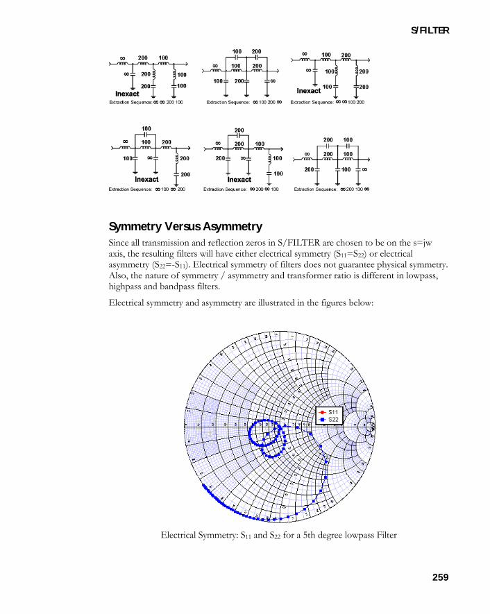
S/FILTER
259
Symmetry Versus Asymmetry Since all transmission and reflection zeros in S/FILTER are chosen to be on the s=jw axis, the resulting filters will have either electrical symmetry (S11=S22) or electrical asymmetry (S22=-S11). Electrical symmetry of filters does not guarantee physical symmetry. Also, the nature of symmetry / asymmetry and transformer ratio is different in lowpass, highpass and bandpass filters.
Electrical symmetry and asymmetry are illustrated in the figures below:
Electrical Symmetry: S11 and S22 for a 5th degree lowpass Filter
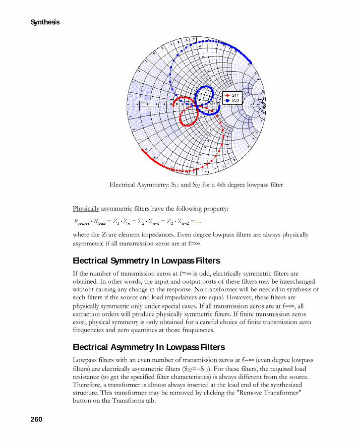
Synthesis
260
Electrical Asymmetry: S11 and S22 for a 4th degree lowpass filter
Physically asymmetric filters have the following property:
where the Zi are element impedances. Even degree lowpass filters are always physically asymmetric if all transmission zeros are at f=∞.
Electrical Symmetry In Lowpass Filters If the number of transmission zeros at f=∞ is odd, electrically symmetric filters are obtained. In other words, the input and output ports of these filters may be interchanged without causing any change in the response. No transformer will be needed in synthesis of such filters if the source and load impedances are equal. However, these filters are physically symmetric only under special cases. If all transmission zeros are at f=∞, all extraction orders will produce physically symmetric filters. If finite transmission zeros exist, physical symmetry is only obtained for a careful choice of finite transmission zero frequencies and zero quantities at those frequencies.
Electrical Asymmetry In Lowpass Filters Lowpass filters with an even number of transmission zeros at f=∞ (even degree lowpass filters) are electrically asymmetric filters (S22=−S11). For these filters, the required load resistance (to get the specified filter characteristics) is always different from the source. Therefore, a transformer is almost always inserted at the load end of the synthesized structure. This transformer may be removed by clicking the "Remove Transformer" button on the Transforms tab.
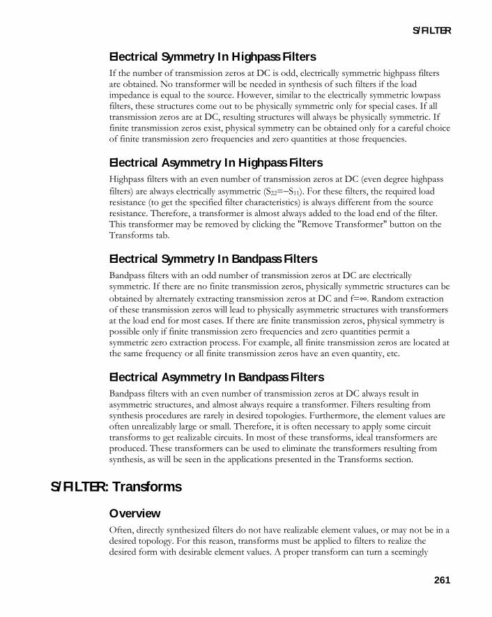
S/FILTER
261
Electrical Symmetry In Highpass Filters If the number of transmission zeros at DC is odd, electrically symmetric highpass filters are obtained. No transformer will be needed in synthesis of such filters if the load impedance is equal to the source. However, similar to the electrically symmetric lowpass filters, these structures come out to be physically symmetric only for special cases. If all transmission zeros are at DC, resulting structures will always be physically symmetric. If finite transmission zeros exist, physical symmetry can be obtained only for a careful choice of finite transmission zero frequencies and zero quantities at those frequencies.
Electrical Asymmetry In Highpass Filters Highpass filters with an even number of transmission zeros at DC (even degree highpass filters) are always electrically asymmetric (S22=−S11). For these filters, the required load resistance (to get the specified filter characteristics) is always different from the source resistance. Therefore, a transformer is almost always added to the load end of the filter. This transformer may be removed by clicking the "Remove Transformer" button on the Transforms tab.
Electrical Symmetry In Bandpass Filters Bandpass filters with an odd number of transmission zeros at DC are electrically symmetric. If there are no finite transmission zeros, physically symmetric structures can be obtained by alternately extracting transmission zeros at DC and f=∞. Random extraction of these transmission zeros will lead to physically asymmetric structures with transformers at the load end for most cases. If there are finite transmission zeros, physical symmetry is possible only if finite transmission zero frequencies and zero quantities permit a symmetric zero extraction process. For example, all finite transmission zeros are located at the same frequency or all finite transmission zeros have an even quantity, etc.
Electrical Asymmetry In Bandpass Filters Bandpass filters with an even number of transmission zeros at DC always result in asymmetric structures, and almost always require a transformer. Filters resulting from synthesis procedures are rarely in desired topologies. Furthermore, the element values are often unrealizably large or small. Therefore, it is often necessary to apply some circuit transforms to get realizable circuits. In most of these transforms, ideal transformers are produced. These transformers can be used to eliminate the transformers resulting from synthesis, as will be seen in the applications presented in the Transforms section.
S/FILTER: Transforms
Overview Often, directly synthesized filters do not have realizable element values, or may not be in a desired topology. For this reason, transforms must be applied to filters to realize the desired form with desirable element values. A proper transform can turn a seemingly

Synthesis
262
unrealizable filter into a form that is very easy to realize. For example, a synthesized filter may have a transformer that can be absorbed into neighboring components by scaling impedances. This is accomplished by using one or more Norton transforms, thus eliminating the transformer.
Norton Transforms
Norton transforms are the basis of most of the circuit transforms that S/FILTER supports. The two basic Norton transforms are the Norton Series transform and the Norton Shunt transform. In these transforms, a single series (shunt) element is replaced by a Tee (Pi) network together with a transformer. Depending on whether the transformer ratio N is greater or less than one, either the left or the right element of Tee and Pi sections is negative. If the transform is carefully applied, negative elements are absorbed by the neighboring positive elements. As an example, consider the filter below. Elements are labeled with "+" or "-" to indicate whether the element's value is greater or less than zero.
To scale the shunt resonator impedances (C2 and L2), a Norton Series transform is applied to the series capacitor (C1). In this transform, "N" is a selectable parameter. The circuit below shows the result of the transform, with dashed components indicating new elements added by the transform.
If N is chosen less than one, C1 is negative and C3 is positive. In this case, there is no other element in the network that can absorb the negative capacitance, since there is no capacitor in parallel with C1. On the other hand, if N is chosen greater than one, C1 is positive and C3 is negative. In this case, if |C4| > |C3|, C4 can absorb the negative element by combining the two parallel capacitances.
By carefully choosing where a Norton transform is applied and by carefully choosing parameters, element values can be scaled and new filter topologies can be explored. In fact, many popular topologies, such as Top-C Coupled bandpass filters, are designed by applying transforms to directly synthesized filters.
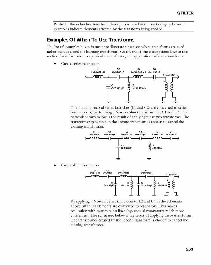
S/FILTER
263
Note: In the individual transform descriptions listed in this section, gray boxes in examples indicate elements affected by the transform being applied.
Examples Of When To Use Transforms The list of examples below is meant to illustrate situations where transforms are used rather than as a tool for learning transforms. See the transform descriptions later in this section for information on particular transforms, and applications of each transform.
• Create series resonators
The first and second series branches (L1 and C2) are converted to series resonators by performing a Norton Shunt transform on C1 and L2. The network shown below is the result of applying these two transforms. The transformer generated in the second transform is chosen to cancel the existing transformer.
• Create shunt resonators
By applying a Norton Series transform to L2 and C4 in the schematic above, all shunt elements are converted to resonators. This makes realization with transmission lines (e.g. coaxial resonators) much more convenient. The schematic below is the result of applying these transforms. The transformer created by the second transform is chosen to cancel the existing transformer.
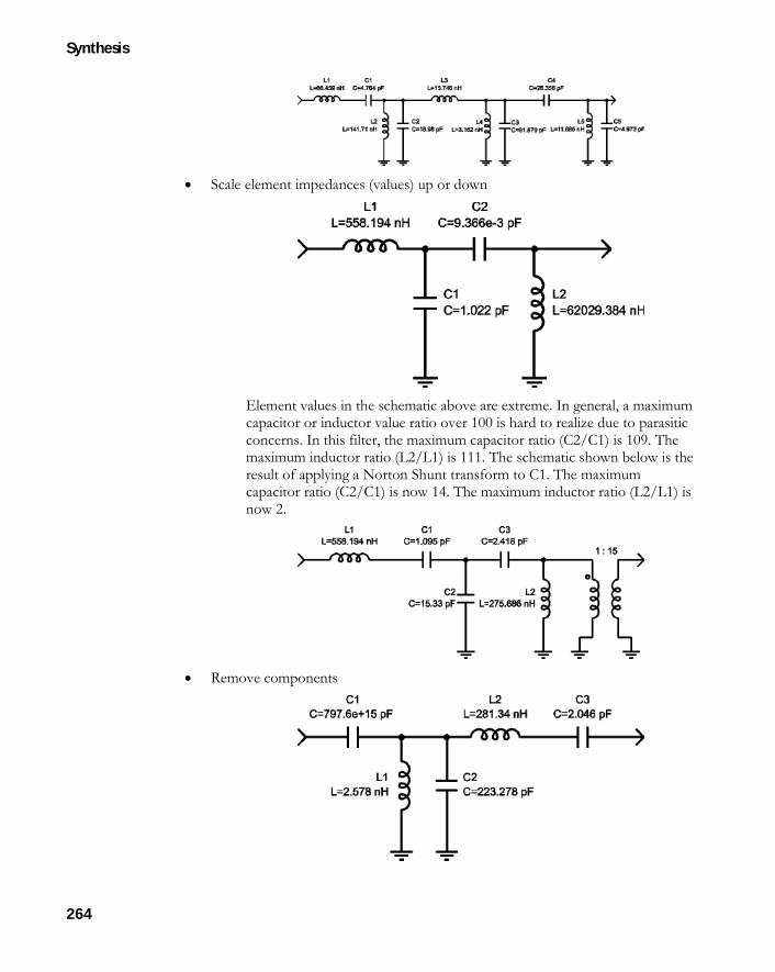
Synthesis
264
• Scale element impedances (values) up or down
Element values in the schematic above are extreme. In general, a maximum capacitor or inductor value ratio over 100 is hard to realize due to parasitic concerns. In this filter, the maximum capacitor ratio (C2/C1) is 109. The maximum inductor ratio (L2/L1) is 111. The schematic shown below is the result of applying a Norton Shunt transform to C1. The maximum capacitor ratio (C2/C1) is now 14. The maximum inductor ratio (L2/L1) is now 2.
• Remove components
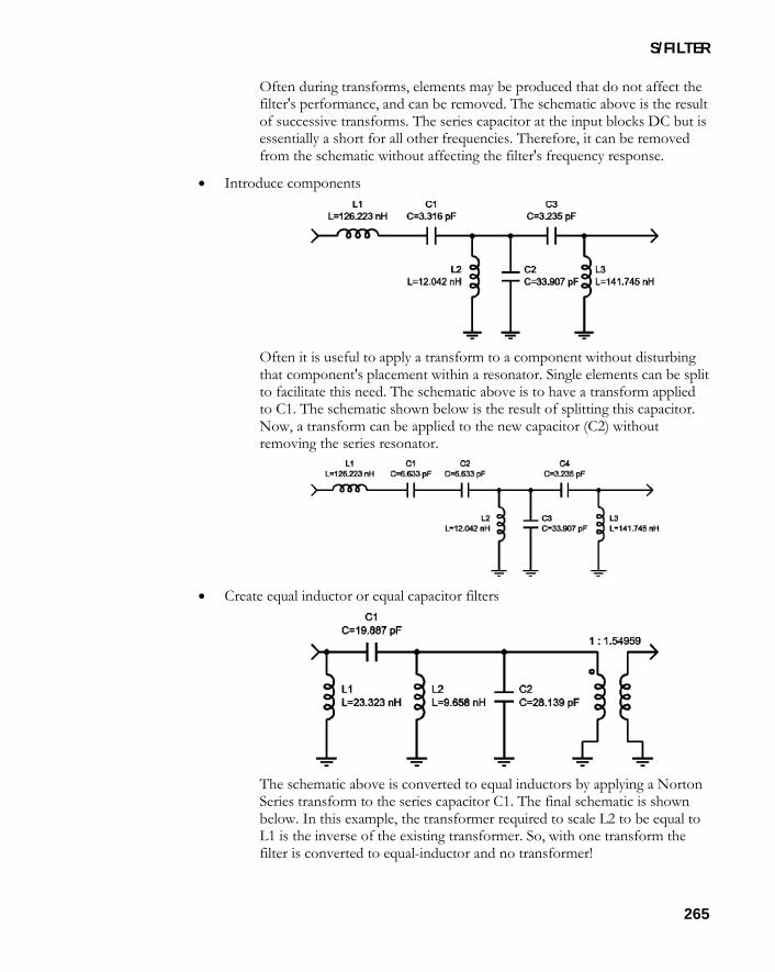
S/FILTER
265
Often during transforms, elements may be produced that do not affect the filter's performance, and can be removed. The schematic above is the result of successive transforms. The series capacitor at the input blocks DC but is essentially a short for all other frequencies. Therefore, it can be removed from the schematic without affecting the filter's frequency response.
• Introduce components
Often it is useful to apply a transform to a component without disturbing that component's placement within a resonator. Single elements can be split to facilitate this need. The schematic above is to have a transform applied to C1. The schematic shown below is the result of splitting this capacitor. Now, a transform can be applied to the new capacitor (C2) without removing the series resonator.
• Create equal inductor or equal capacitor filters
The schematic above is converted to equal inductors by applying a Norton Series transform to the series capacitor C1. The final schematic is shown below. In this example, the transformer required to scale L2 to be equal to L1 is the inverse of the existing transformer. So, with one transform the filter is converted to equal-inductor and no transformer!

Synthesis
266
Basic Operations
Split Series Element Into 2 Parts Transform Description
This transform splits a series element into two equal series elements. The combined value of the two series elements is equivalent to the original element value. This transform is shown below:
Before Transform: After Transform:
Example
Basic Equations
The equations for this transform depend on the element being split. Most elements, including transmission lines, can be split. Some supported elements and their equations for two equal pieces are shown below:
Before Transform: After Transform: Equation(s):

S/FILTER
267
Note: Although this transform will split parallel resonators in series into two resonators, these separate resonators cannot be recombined with the Simplify button. This is because although a single finite zero can be realized with two separate resonators, a single resonator cannot realize more than one finite zero. Therefore, S/FILTER will not combine separate resonators into one even if they have the same resonant frequency.
Options
You may split the part into 2 equal, 3 equal, or 2 unequal pieces. You may also split a quad resonator into two resonators.
Split Shunt Element Into 2 Parts Transform Description
This transform splits a shunt element into two equal shunt elements. The combined value of the two shunt elements is equivalent to the original element value. This transform is shown below:
Before Transform: After Transform:
Example
Basic Equations
The equations for this transform depend on the element being split. Most elements, including transmission lines, can be split. Some supported elements and their equations for two equal pieces are shown below:
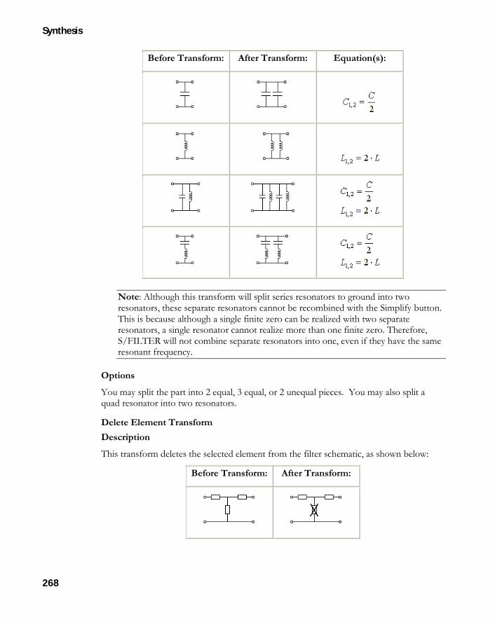
Synthesis
268
Before Transform: After Transform: Equation(s):
Note: Although this transform will split series resonators to ground into two resonators, these separate resonators cannot be recombined with the Simplify button. This is because although a single finite zero can be realized with two separate resonators, a single resonator cannot realize more than one finite zero. Therefore, S/FILTER will not combine separate resonators into one, even if they have the same resonant frequency.
Options
You may split the part into 2 equal, 3 equal, or 2 unequal pieces. You may also split a quad resonator into two resonators.
Delete Element Transform Description
This transform deletes the selected element from the filter schematic, as shown below:
Before Transform: After Transform:

S/FILTER
269
Example
Basic Equations
There are no equations for this transform.
Options
There are no options for this transform.
Insert Element Description
This transform inserts an element into the filter schematic, as shown below:
Before Transform: After Transform:
Basic Equations
There are no equations for this transform.
Options
You may pick the type, orientation, and value of the inserted element.
Swap Element With The One To The Right Transform Description
This transform swaps the selected element with the element located to the right, as shown below:
Before Transform: After Transform:
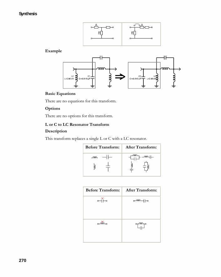
Synthesis
270
Example
Basic Equations
There are no equations for this transform.
Options
There are no options for this transform.
L or C to LC Resonator Transform Description
This transform replaces a single L or C with a LC resonator.
Before Transform: After Transform:
Before Transform: After Transform:
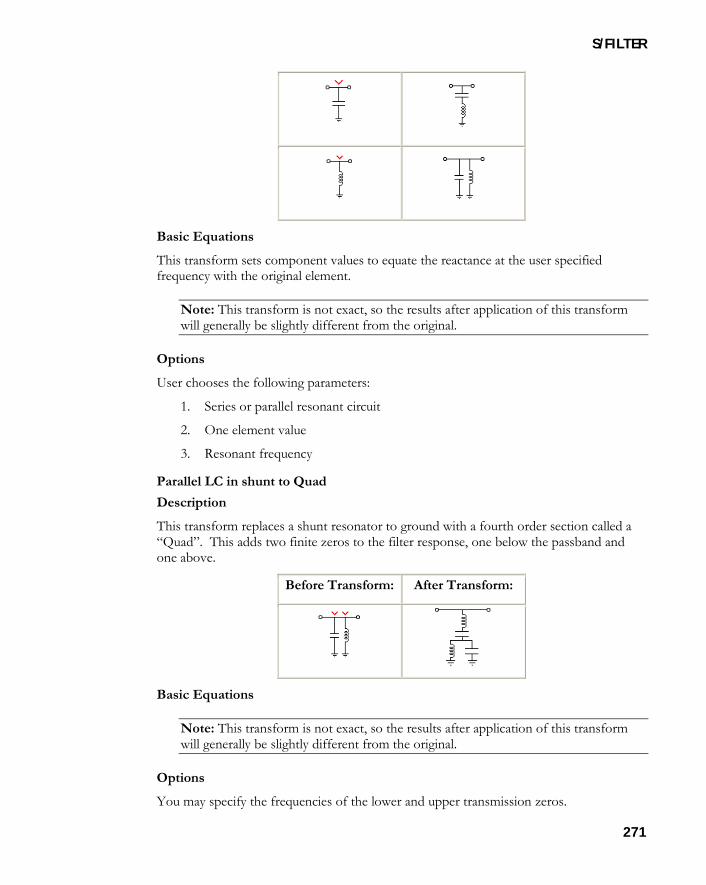
S/FILTER
271
Basic Equations
This transform sets component values to equate the reactance at the user specified frequency with the original element.
Note: This transform is not exact, so the results after application of this transform will generally be slightly different from the original.
Options User chooses the following parameters:
1. Series or parallel resonant circuit
2. One element value
3. Resonant frequency
Parallel LC in shunt to Quad Description
This transform replaces a shunt resonator to ground with a fourth order section called a “Quad”. This adds two finite zeros to the filter response, one below the passband and one above.
Before Transform: After Transform:
Basic Equations
Note: This transform is not exact, so the results after application of this transform will generally be slightly different from the original.
Options You may specify the frequencies of the lower and upper transmission zeros.
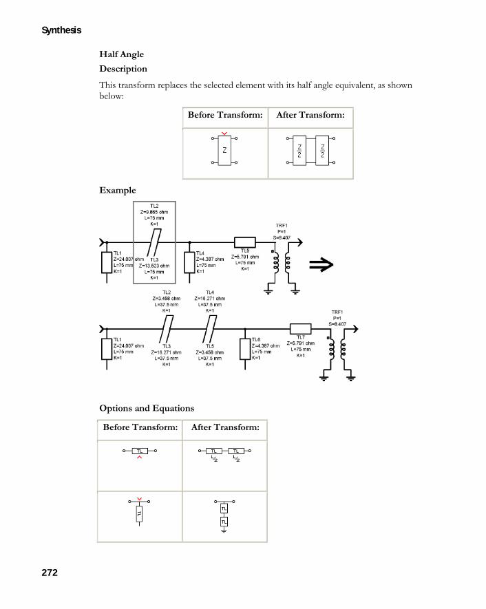
Synthesis
272
Half Angle Description
This transform replaces the selected element with its half angle equivalent, as shown below:
Before Transform: After Transform:
Example
Options and Equations
Before Transform: After Transform:
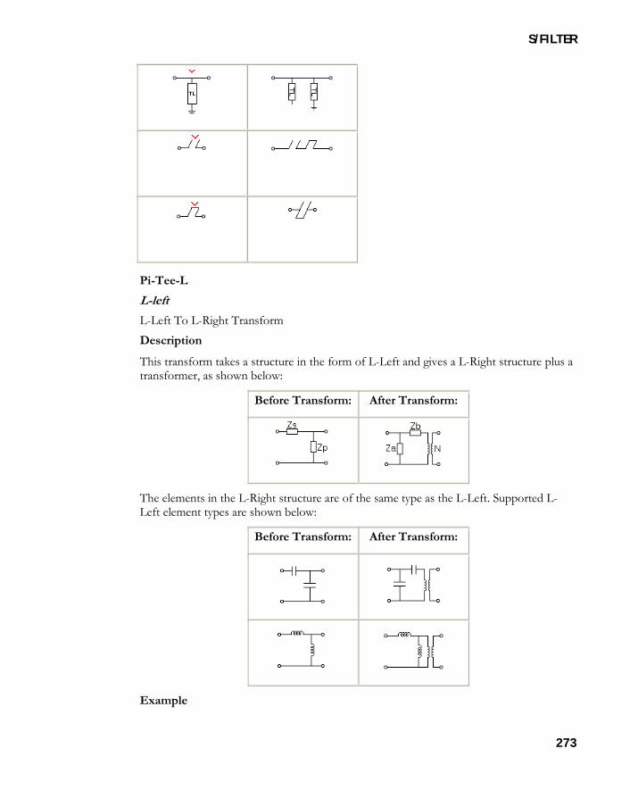
S/FILTER
273
Pi-Tee-L L-left L-Left To L-Right Transform Description
This transform takes a structure in the form of L-Left and gives a L-Right structure plus a transformer, as shown below:
Before Transform: After Transform:
The elements in the L-Right structure are of the same type as the L-Left. Supported L-Left element types are shown below:
Before Transform: After Transform:
Example

Synthesis
274
Basic Equations
The equations for the L-Left To L-Right Transform are shown below:
Options
There are no options for this transform.
L-left to Pi Description
This transform takes a structure in the form of L-Left and gives a pi structure plus a transformer, as shown below:
Before Transform: After Transform:
Options
There are no options for this transform.
L-Left To Pi Transform Description
This transform takes a structure in the form of L-Left and gives a Pi structure plus a transformer, as shown below:
Before Transform: After Transform:
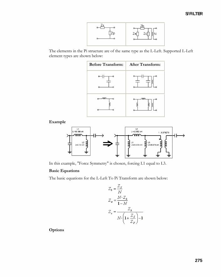
S/FILTER
275
The elements in the Pi structure are of the same type as the L-Left. Supported L-Left element types are shown below:
Before Transform: After Transform:
Example
In this example, "Force Symmetry" is chosen, forcing L1 equal to L3.
Basic Equations
The basic equations for the L-Left To Pi Transform are shown below:
Options
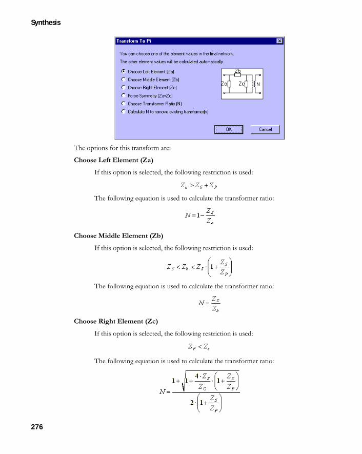
Synthesis
276
The options for this transform are:
Choose Left Element (Za) If this option is selected, the following restriction is used:
The following equation is used to calculate the transformer ratio:
Choose Middle Element (Zb) If this option is selected, the following restriction is used:
The following equation is used to calculate the transformer ratio:
Choose Right Element (Zc)
If this option is selected, the following restriction is used:
The following equation is used to calculate the transformer ratio:
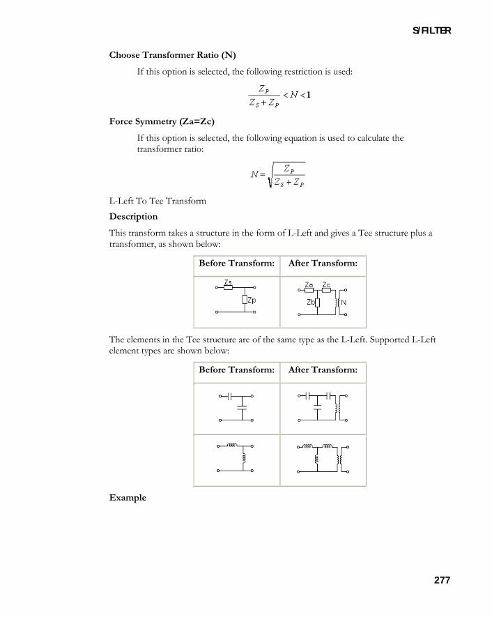
S/FILTER
277
Choose Transformer Ratio (N) If this option is selected, the following restriction is used:
Force Symmetry (Za=Zc)
If this option is selected, the following equation is used to calculate the transformer ratio:
L-Left To Tee Transform Description
This transform takes a structure in the form of L-Left and gives a Tee structure plus a transformer, as shown below:
Before Transform: After Transform:
The elements in the Tee structure are of the same type as the L-Left. Supported L-Left element types are shown below:
Before Transform: After Transform:
Example

Synthesis
278
In this example, the center element is chosen as 10 nH.
Basic Equations
The basic equations for the L-Left To Tee Transform are shown below:
Options
The options for this transform are:
Choose Left Element (Za) If this option is selected, the following restriction is used:
The following equation is used to calculate the transformer ratio:
Choose Middle Element (Zb)
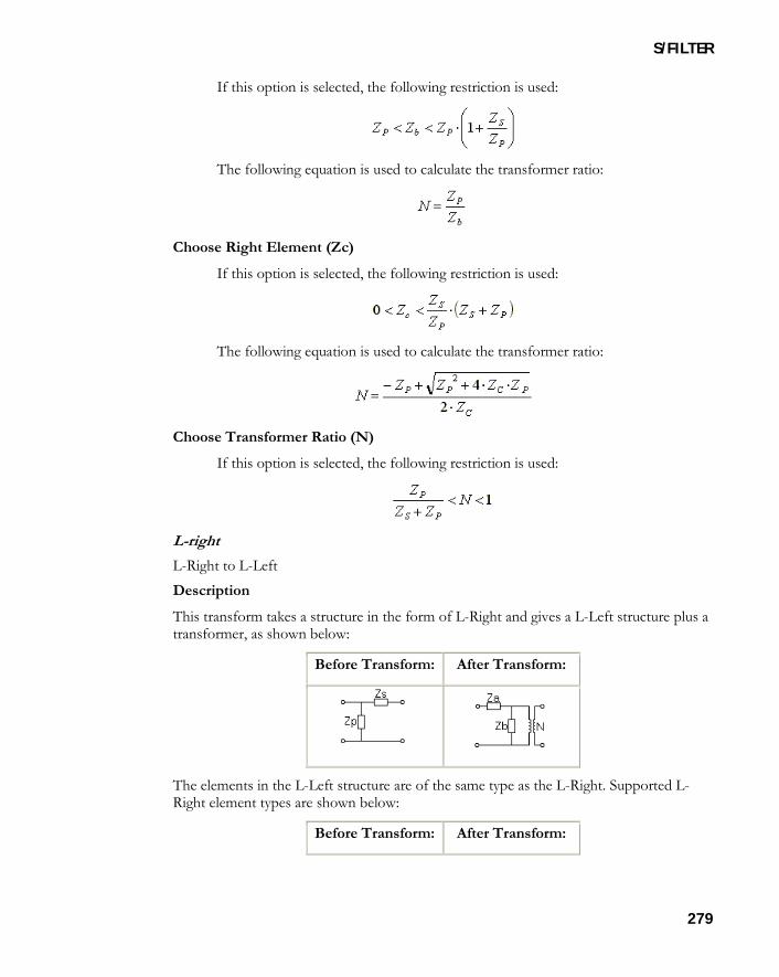
S/FILTER
279
If this option is selected, the following restriction is used:
The following equation is used to calculate the transformer ratio:
Choose Right Element (Zc)
If this option is selected, the following restriction is used:
The following equation is used to calculate the transformer ratio:
Choose Transformer Ratio (N)
If this option is selected, the following restriction is used:
L-right L-Right to L-Left Description This transform takes a structure in the form of L-Right and gives a L-Left structure plus a transformer, as shown below:
Before Transform: After Transform:
The elements in the L-Left structure are of the same type as the L-Right. Supported L-Right element types are shown below:
Before Transform: After Transform:
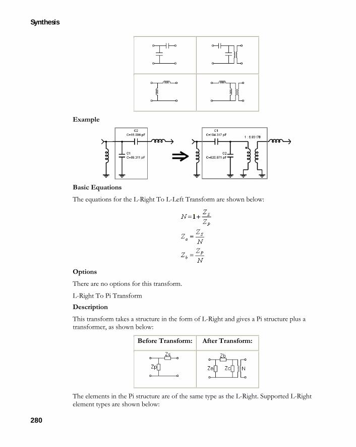
Synthesis
280
Example
Basic Equations
The equations for the L-Right To L-Left Transform are shown below:
Options
There are no options for this transform.
L-Right To Pi Transform Description
This transform takes a structure in the form of L-Right and gives a Pi structure plus a transformer, as shown below:
Before Transform: After Transform:
The elements in the Pi structure are of the same type as the L-Right. Supported L-Right element types are shown below:
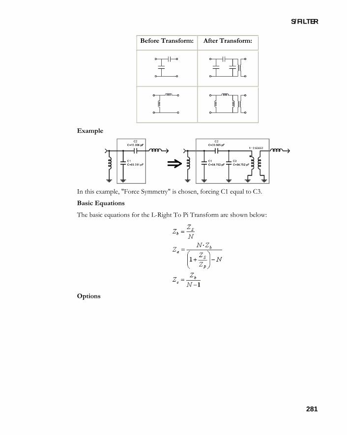
S/FILTER
281
Before Transform: After Transform:
Example
In this example, "Force Symmetry" is chosen, forcing C1 equal to C3.
Basic Equations
The basic equations for the L-Right To Pi Transform are shown below:
Options

Synthesis
282
The options for this transform are:
Choose Left Element (Za) If this option is selected, the following restriction is used:
The following equation is used to calculate the transformer ratio:
Choose Middle Element (Zb) If this option is selected, the following restriction is used:
The following equation is used to calculate the transformer ratio:
Choose Right Element (Zc)
If this option is selected, the following restriction is used:
The following equation is used to calculate the transformer ratio:
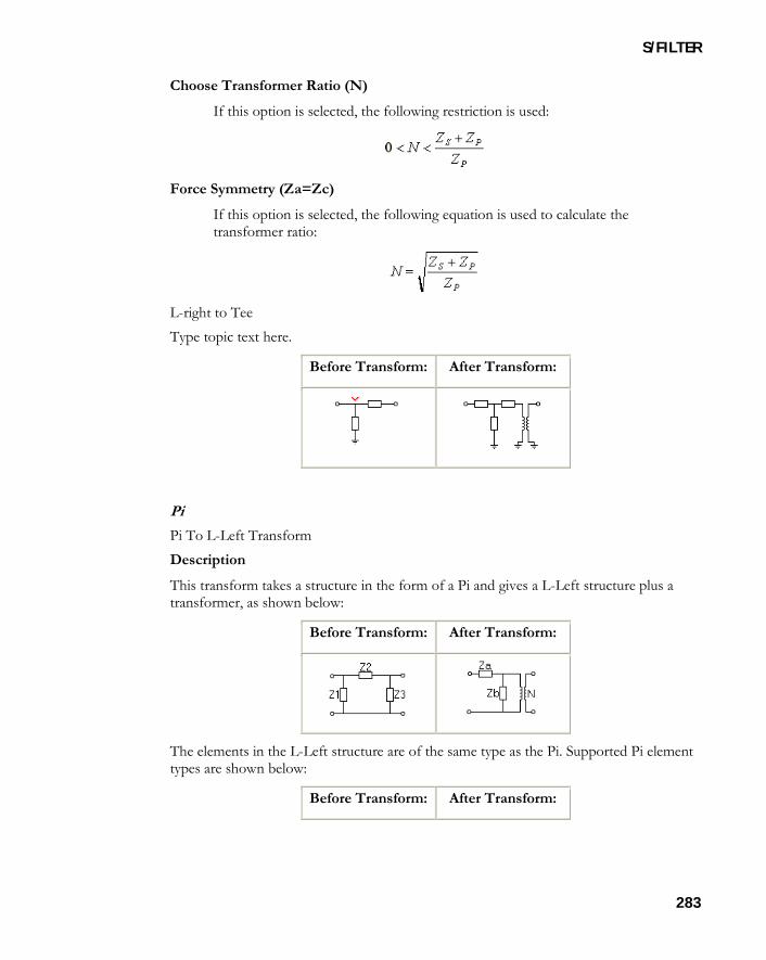
S/FILTER
283
Choose Transformer Ratio (N) If this option is selected, the following restriction is used:
Force Symmetry (Za=Zc)
If this option is selected, the following equation is used to calculate the transformer ratio:
L-right to Tee Type topic text here.
Before Transform: After Transform:
Pi Pi To L-Left Transform Description
This transform takes a structure in the form of a Pi and gives a L-Left structure plus a transformer, as shown below:
Before Transform: After Transform:
The elements in the L-Left structure are of the same type as the Pi. Supported Pi element types are shown below:
Before Transform: After Transform:

Synthesis
284
Example
Basic Equations
The equations for the Pi To L-Left Transform are shown below:
Options
There are no options for this transform.
Pi to L-right Type topic text here.
Before Transform: After Transform:
Pi To Tee Transform
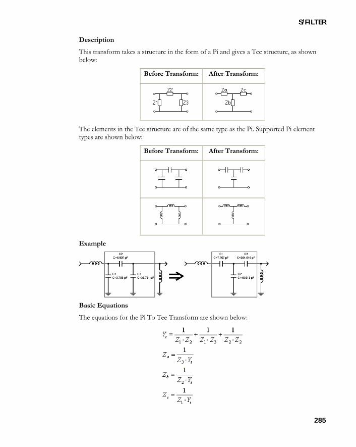
S/FILTER
285
Description
This transform takes a structure in the form of a Pi and gives a Tee structure, as shown below:
Before Transform: After Transform:
The elements in the Tee structure are of the same type as the Pi. Supported Pi element types are shown below:
Before Transform: After Transform:
Example
Basic Equations
The equations for the Pi To Tee Transform are shown below:
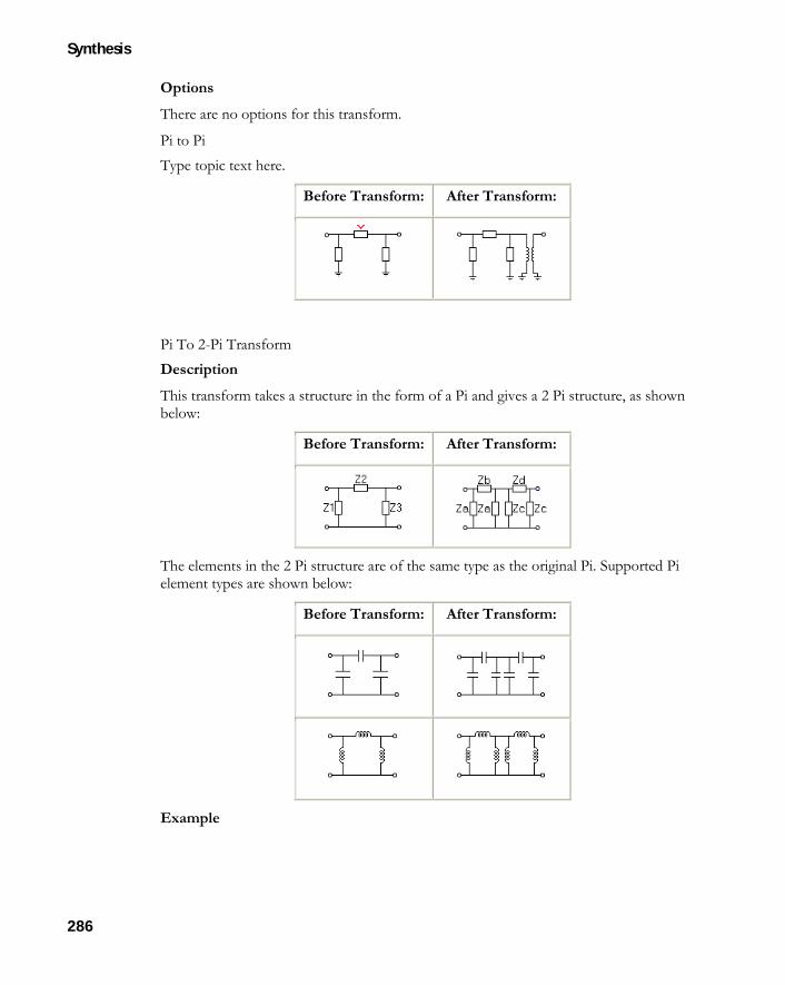
Synthesis
286
Options
There are no options for this transform.
Pi to Pi Type topic text here.
Before Transform: After Transform:
Pi To 2-Pi Transform Description
This transform takes a structure in the form of a Pi and gives a 2 Pi structure, as shown below:
Before Transform: After Transform:
The elements in the 2 Pi structure are of the same type as the original Pi. Supported Pi element types are shown below:
Before Transform: After Transform:
Example
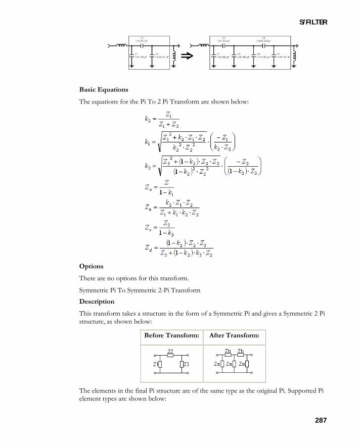
S/FILTER
287
Basic Equations
The equations for the Pi To 2 Pi Transform are shown below:
Options
There are no options for this transform.
Symmetric Pi To Symmetric 2-Pi Transform Description
This transform takes a structure in the form of a Symmetric Pi and gives a Symmetric 2 Pi structure, as shown below:
Before Transform: After Transform:
The elements in the final Pi structure are of the same type as the original Pi. Supported Pi element types are shown below:
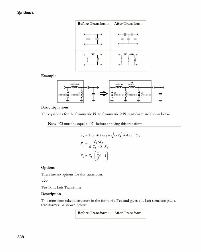
Synthesis
288
Before Transform: After Transform:
Example
Basic Equations
The equations for the Symmetric Pi To Symmetric 2 Pi Transform are shown below:
Note: Z3 must be equal to Z1 before applying this transform.
Options
There are no options for this transform.
Tee Tee To L-Left Transform Description
This transform takes a structure in the form of a Tee and gives a L-Left structure plus a transformer, as shown below:
Before Transform: After Transform:
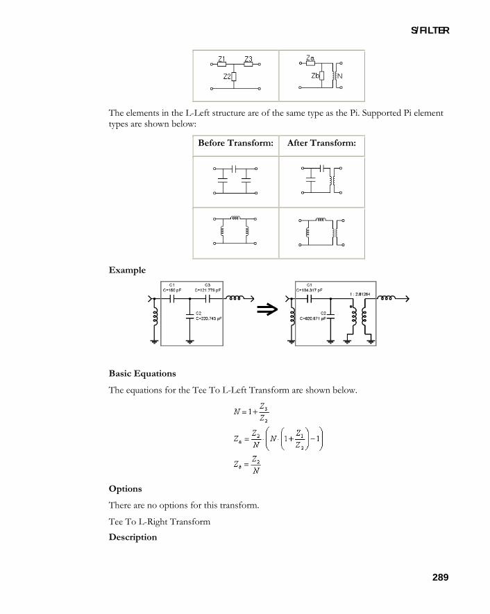
S/FILTER
289
The elements in the L-Left structure are of the same type as the Pi. Supported Pi element types are shown below:
Before Transform: After Transform:
Example
Basic Equations
The equations for the Tee To L-Left Transform are shown below.
Options
There are no options for this transform.
Tee To L-Right Transform Description
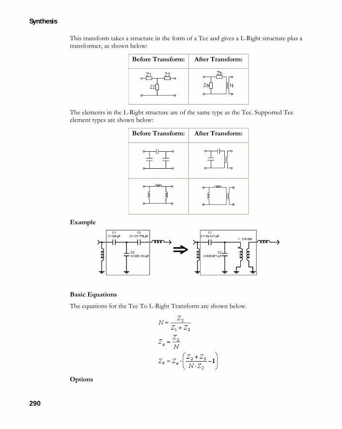
Synthesis
290
This transform takes a structure in the form of a Tee and gives a L-Right structure plus a transformer, as shown below:
Before Transform: After Transform:
The elements in the L-Right structure are of the same type as the Tee. Supported Tee element types are shown below:
Before Transform: After Transform:
Example
Basic Equations
The equations for the Tee To L-Right Transform are shown below.
Options
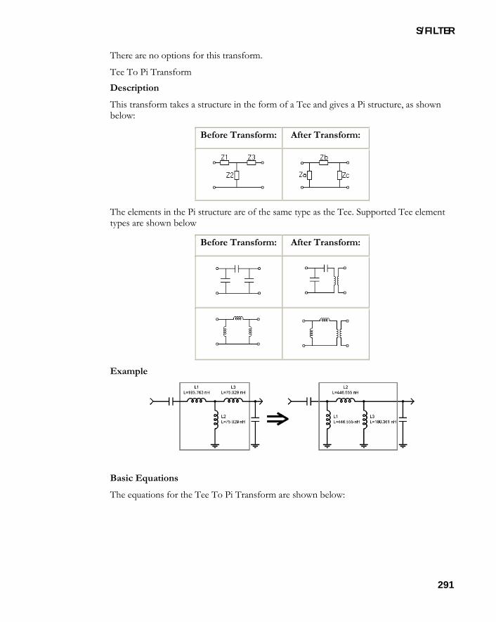
S/FILTER
291
There are no options for this transform.
Tee To Pi Transform Description
This transform takes a structure in the form of a Tee and gives a Pi structure, as shown below:
Before Transform: After Transform:
The elements in the Pi structure are of the same type as the Tee. Supported Tee element types are shown below
Before Transform: After Transform:
Example
Basic Equations
The equations for the Tee To Pi Transform are shown below:
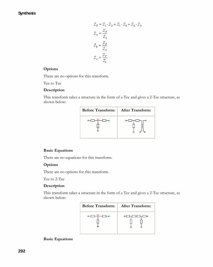
Synthesis
292
Options
There are no options for this transform.
Tee to Tee Description
This transform takes a structure in the form of a Tee and gives a 2-Tee structure, as shown below:
Before Transform: After Transform:
Basic Equations
There are no equations for this transform.
Options
There are no options for this transform.
Tee to 2-Tee Description
This transform takes a structure in the form of a Tee and gives a 2-Tee structure, as shown below:
Before Transform: After Transform:
Basic Equations
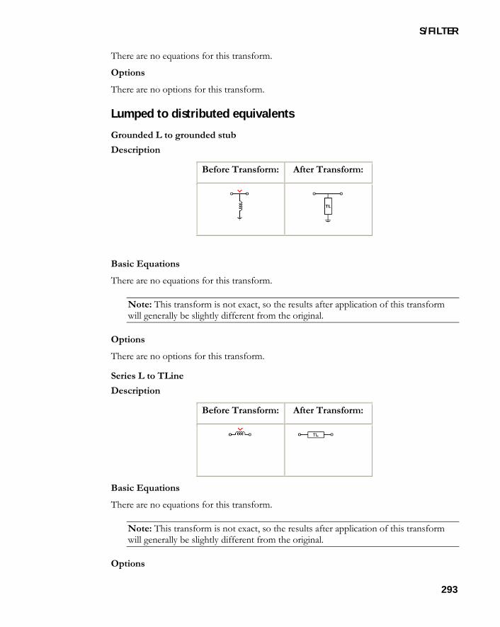
S/FILTER
293
There are no equations for this transform.
Options
There are no options for this transform.
Lumped to distributed equivalents
Grounded L to grounded stub Description
Before Transform: After Transform:
Basic Equations
There are no equations for this transform.
Note: This transform is not exact, so the results after application of this transform will generally be slightly different from the original.
Options There are no options for this transform.
Series L to TLine Description
Before Transform: After Transform:
Basic Equations
There are no equations for this transform.
Note: This transform is not exact, so the results after application of this transform will generally be slightly different from the original.
Options
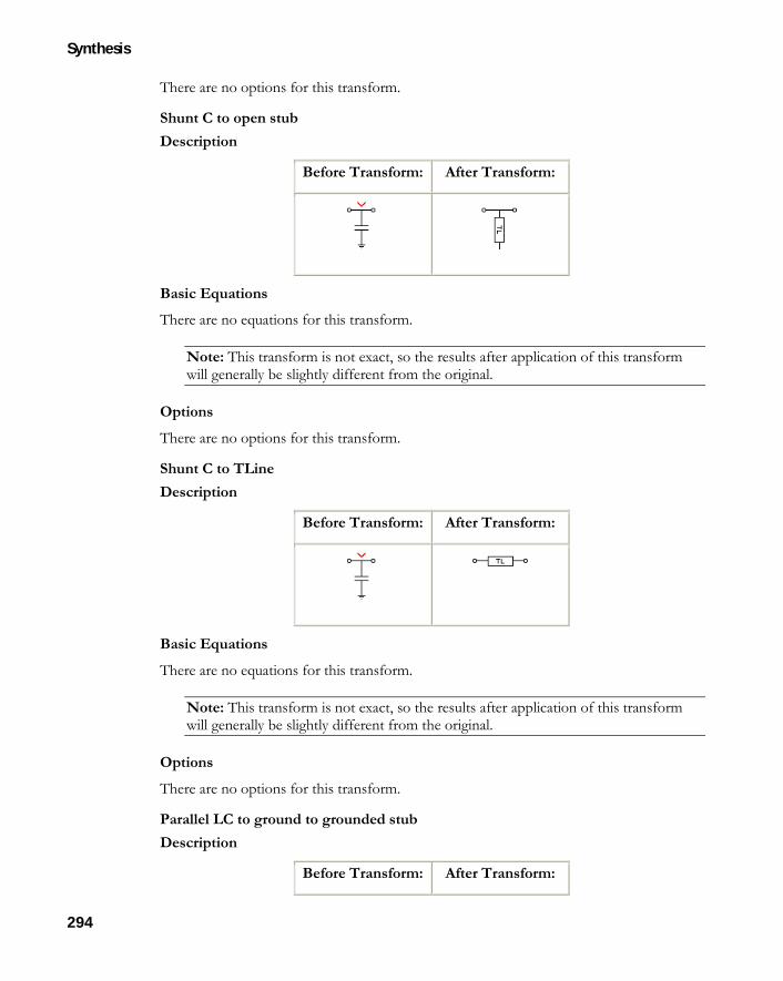
Synthesis
294
There are no options for this transform.
Shunt C to open stub Description
Before Transform: After Transform:
Basic Equations
There are no equations for this transform.
Note: This transform is not exact, so the results after application of this transform will generally be slightly different from the original.
Options There are no options for this transform.
Shunt C to TLine Description
Before Transform: After Transform:
Basic Equations
There are no equations for this transform.
Note: This transform is not exact, so the results after application of this transform will generally be slightly different from the original.
Options There are no options for this transform.
Parallel LC to ground to grounded stub Description
Before Transform: After Transform:
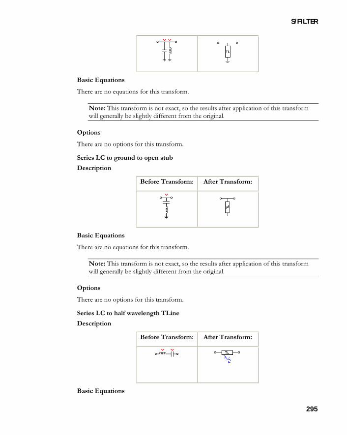
S/FILTER
295
Basic Equations
There are no equations for this transform.
Note: This transform is not exact, so the results after application of this transform will generally be slightly different from the original.
Options There are no options for this transform.
Series LC to ground to open stub Description
Before Transform: After Transform:
Basic Equations
There are no equations for this transform.
Note: This transform is not exact, so the results after application of this transform will generally be slightly different from the original.
Options There are no options for this transform.
Series LC to half wavelength TLine Description
Before Transform: After Transform:
Basic Equations
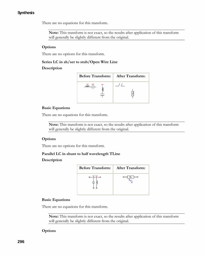
Synthesis
296
There are no equations for this transform.
Note: This transform is not exact, so the results after application of this transform will generally be slightly different from the original.
Options There are no options for this transform.
Series LC in sh/ser to stub/Open Wire Line Description
Before Transform: After Transform:
Basic Equations
There are no equations for this transform.
Note: This transform is not exact, so the results after application of this transform will generally be slightly different from the original.
Options There are no options for this transform.
Parallel LC in shunt to half wavelength TLine Description
Before Transform: After Transform:
Basic Equations
There are no equations for this transform.
Note: This transform is not exact, so the results after application of this transform will generally be slightly different from the original.
Options
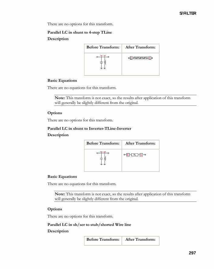
S/FILTER
297
There are no options for this transform.
Parallel LC in shunt to 4-step TLine Description
Before Transform: After Transform:
Basic Equations
There are no equations for this transform.
Note: This transform is not exact, so the results after application of this transform will generally be slightly different from the original.
Options There are no options for this transform.
Parallel LC in shunt to Inverter-TLine-Inverter Description
Before Transform: After Transform:
Basic Equations
There are no equations for this transform.
Note: This transform is not exact, so the results after application of this transform will generally be slightly different from the original.
Options There are no options for this transform.
Parallel LC in sh/ser to stub/shorted Wire line Description
Before Transform: After Transform:
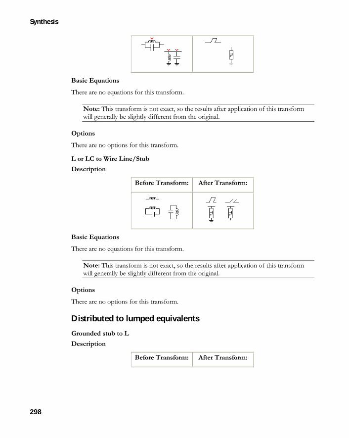
Synthesis
298
Basic Equations
There are no equations for this transform.
Note: This transform is not exact, so the results after application of this transform will generally be slightly different from the original.
Options There are no options for this transform.
L or LC to Wire Line/Stub Description
Before Transform: After Transform:
Basic Equations
There are no equations for this transform.
Note: This transform is not exact, so the results after application of this transform will generally be slightly different from the original.
Options There are no options for this transform.
Distributed to lumped equivalents
Grounded stub to L Description
Before Transform: After Transform:
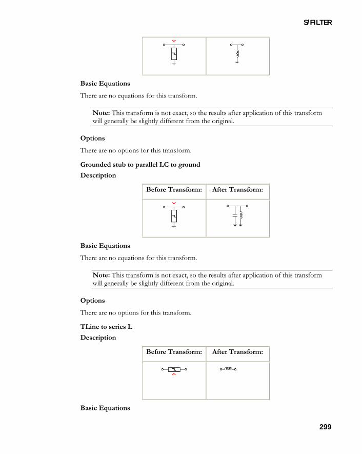
S/FILTER
299
Basic Equations
There are no equations for this transform.
Note: This transform is not exact, so the results after application of this transform will generally be slightly different from the original.
Options There are no options for this transform.
Grounded stub to parallel LC to ground Description
Before Transform: After Transform:
Basic Equations
There are no equations for this transform.
Note: This transform is not exact, so the results after application of this transform will generally be slightly different from the original.
Options There are no options for this transform.
TLine to series L Description
Before Transform: After Transform:
Basic Equations
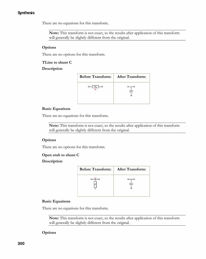
Synthesis
300
There are no equations for this transform.
Note: This transform is not exact, so the results after application of this transform will generally be slightly different from the original.
Options There are no options for this transform.
TLine to shunt C Description
Before Transform: After Transform:
Basic Equations
There are no equations for this transform.
Note: This transform is not exact, so the results after application of this transform will generally be slightly different from the original.
Options There are no options for this transform.
Open stub to shunt C Description
Before Transform: After Transform:
Basic Equations
There are no equations for this transform.
Note: This transform is not exact, so the results after application of this transform will generally be slightly different from the original.
Options

S/FILTER
301
There are no options for this transform.
Open stub to series LC to ground Description
Before Transform: After Transform:
Basic Equations
There are no equations for this transform.
Note: This transform is not exact, so the results after application of this transform will generally be slightly different from the original.
Options There are no options for this transform.
Series half wavelenth TLine to series LC Description
Before Transform: After Transform:
Basic Equations
There are no equations for this transform.
Note: This transform is not exact, so the results after application of this transform will generally be slightly different from the original.
Options There are no options for this transform.
TLine to Inductive and Capacitive Tee Description
Before Transform: After Transform:

Synthesis
302
Basic Equations
There are no equations for this transform.
Note: This transform is not exact, so the results after application of this transform will generally be slightly different from the original.
Options There are no options for this transform.
TLine to Inductive and Capacitive Pi Description
Before Transform: After Transform:
Basic Equations
There are no equations for this transform.
Note: This transform is not exact, so the results after application of this transform will generally be slightly different from the original.
Options There are no options for this transform.
Wire Line/stub to single L or C Description
Before Transform: After Transform:
Basic Equations
S/FILTER
303
There are no equations for this transform.
Note: This transform is not exact, so the results after application of this transform will generally be slightly different from the original.
Options There are no options for this transform.
Wire Line/stub to LC Resonator Description
Before Transform: After Transform:
Basic Equations
There are no equations for this transform.
Note: This transform is not exact, so the results after application of this transform will generally be slightly different from the original.
Options There are no options for this transform.
Compound Operations
Find dual of schematic Description
This transform finds the dual representation of the filter schematic. Applying this transform is analogous to checking or un-checking the "Series Element First" checkbox on the Extractions tab.
Before Transform: After Transform:
Basic Equations
There are no equations for this transform.

Synthesis
304
Options
There are no options for this transform.
Equate all L's Description
This transform applies Norton transforms to the filter to make all inductors equal. If the transform is successful, all inductors are made equal to the leftmost inductor’s value.
Before Transform: After Transform:
Basic Equations
There are no equations for this transform.
Options
There are no options for this transform.
Equate all C's Description
This transform applies Norton transforms to the filter to make all capacitors equal. If the transform is successful, all capacitors are made equal to the leftmost capacitor’s value.
Before Transform: After Transform:
Basic Equations
There are no equations for this transform.
Options
There are no options for this transform.
Equate all shunt L's or shorted stubs This transform applies Tee and Pi transforms to the filter to make all shunt capacitors or open stubs equal. If the transform is successful, all shunt capacitors (open stubs) are made equal to the leftmost capacitor’s value.
S/FILTER
305
Before Transform: After Transform:
Basic Equations
There are no equations for this transform.
Options
There are no options for this transform.
Equate all shunt C's or open stubs Description
This transform applies Tee and Pi transforms to the filter to make all shunt capacitors or open stubs equal. If the transform is successful, all shunt capacitors (open stubs) are made equal to the leftmost capacitor’s value.
Before Transform: After Transform:
Basic Equations
There are no equations for this transform.
Options
There are no options for this transform.
Transformer Operations
Shift left by one Description
This transform moves the selected transformer leftmost (adjacent to the source) as shown below:
Before Transform: After Transform:
Synthesis
306
Example
Basic Equations
This transform scales all elements between the transformer and source. The equations for this scaling depend on the element type:
Elements: Equation(s):
Options
There are no options for this transform.
Shift leftmost Description
This transform moves the selected transformer leftmost (adjacent to the source) as shown below:
Before Transform: After Transform:
S/FILTER
307
Example
Basic Equations
This transform scales all elements between the transformer and source. The equations for this scaling depend on the element type:
Elements: Equation(s):
Options
There are no options for this transform.
Shift right by one Description
This transform moves the selected transformer to the right by one element, as shown below:
Before Transform: After Transform:
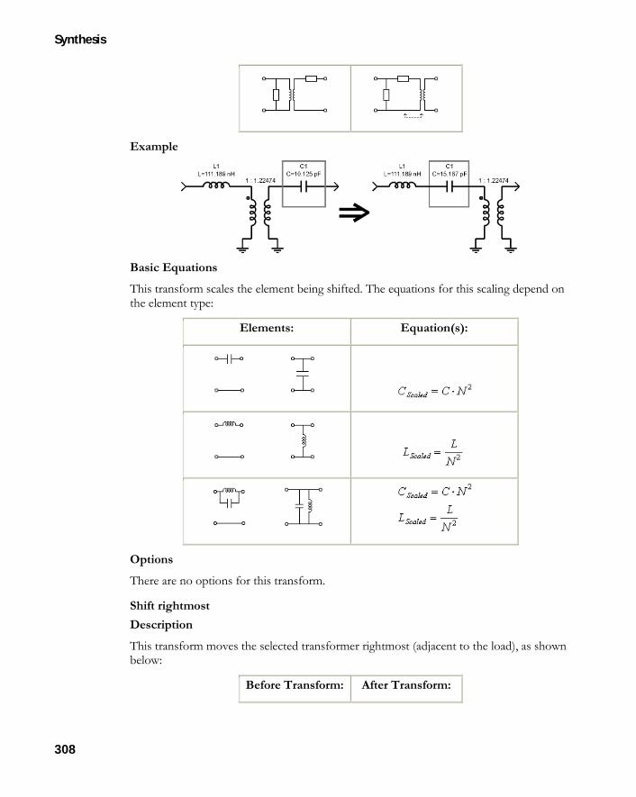
Synthesis
308
Example
Basic Equations
This transform scales the element being shifted. The equations for this scaling depend on the element type:
Elements: Equation(s):
Options
There are no options for this transform.
Shift rightmost Description
This transform moves the selected transformer rightmost (adjacent to the load), as shown below:
Before Transform: After Transform:
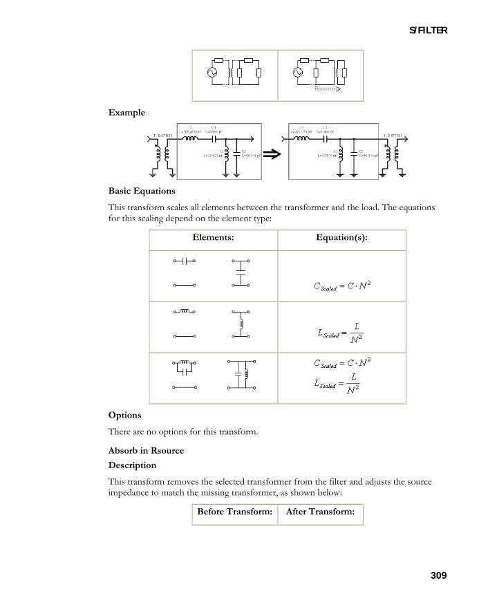
S/FILTER
309
Example
Basic Equations
This transform scales all elements between the transformer and the load. The equations for this scaling depend on the element type:
Elements: Equation(s):
Options
There are no options for this transform.
Absorb in Rsource Description
This transform removes the selected transformer from the filter and adjusts the source impedance to match the missing transformer, as shown below:
Before Transform: After Transform:
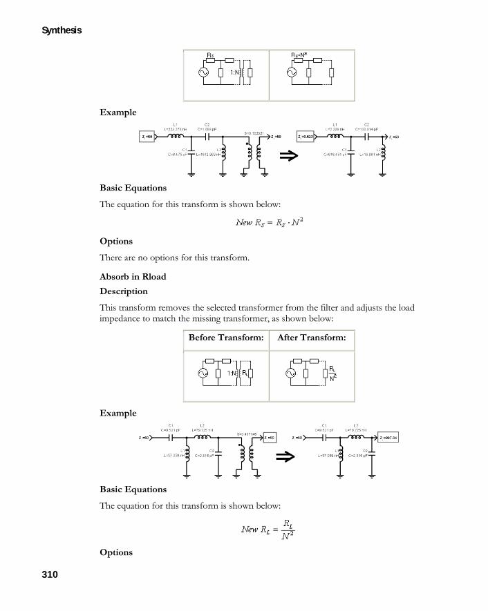
Synthesis
310
Example
Basic Equations
The equation for this transform is shown below:
Options
There are no options for this transform.
Absorb in Rload Description
This transform removes the selected transformer from the filter and adjusts the load impedance to match the missing transformer, as shown below:
Before Transform: After Transform:
Example
Basic Equations
The equation for this transform is shown below:
Options

S/FILTER
311
There are no options for this transform.
Combine All TRFs Transform Description
This transform shifts all transformers within the filter to the rightmost position and combines all transformers to form one equivalent transformer, as shown below:
Before Transform: After Transform:
Example
Basic Equations
The equation for this transform is shown below:
Options
There are no options for this transform.
Termination Coupling
Source: Series L to Shunt L Description
Before Transform: After Transform:
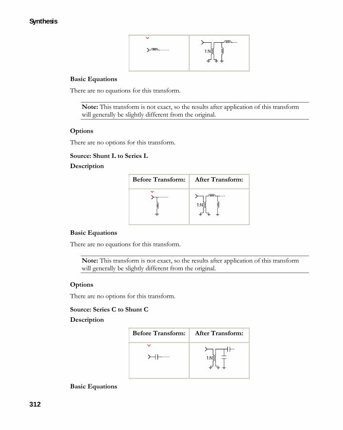
Synthesis
312
Basic Equations
There are no equations for this transform.
Note: This transform is not exact, so the results after application of this transform will generally be slightly different from the original.
Options There are no options for this transform.
Source: Shunt L to Series L Description
Before Transform: After Transform:
Basic Equations
There are no equations for this transform.
Note: This transform is not exact, so the results after application of this transform will generally be slightly different from the original.
Options There are no options for this transform.
Source: Series C to Shunt C Description
Before Transform: After Transform:
Basic Equations
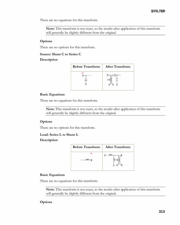
S/FILTER
313
There are no equations for this transform.
Note: This transform is not exact, so the results after application of this transform will generally be slightly different from the original.
Options There are no options for this transform.
Source: Shunt C to Series C Description
Before Transform: After Transform:
Basic Equations
There are no equations for this transform.
Note: This transform is not exact, so the results after application of this transform will generally be slightly different from the original.
Options There are no options for this transform.
Load: Series L to Shunt L Description
Before Transform: After Transform:
Basic Equations
There are no equations for this transform.
Note: This transform is not exact, so the results after application of this transform will generally be slightly different from the original.
Options
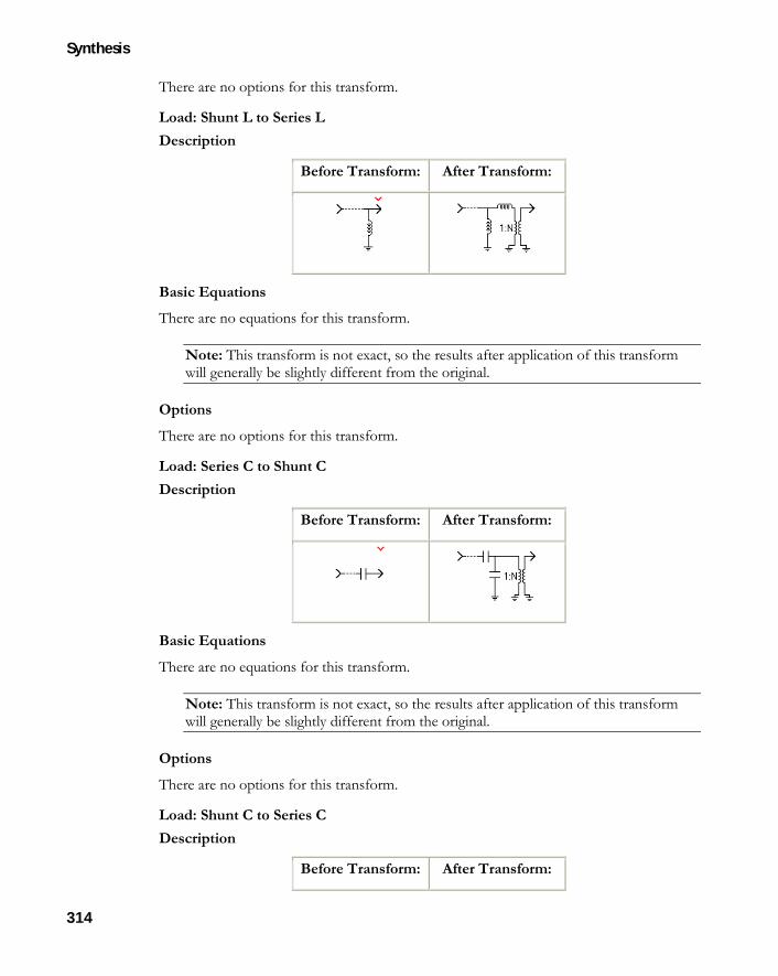
Synthesis
314
There are no options for this transform.
Load: Shunt L to Series L Description
Before Transform: After Transform:
Basic Equations
There are no equations for this transform.
Note: This transform is not exact, so the results after application of this transform will generally be slightly different from the original.
Options There are no options for this transform.
Load: Series C to Shunt C Description
Before Transform: After Transform:
Basic Equations
There are no equations for this transform.
Note: This transform is not exact, so the results after application of this transform will generally be slightly different from the original.
Options There are no options for this transform.
Load: Shunt C to Series C Description
Before Transform: After Transform:

S/FILTER
315
Basic Equations
There are no equations for this transform.
Note: This transform is not exact, so the results after application of this transform will generally be slightly different from the original.
Options There are no options for this transform.
Inverters
Replace element(s) with inverter(s) Description
Before Transform: After Transform:
Basic Equations
There are no equations for this transform.
Note: This transform is not exact, so the results after application of this transform will generally be slightly different from the original.
Options There are no options for this transform.
Scale Inverter Description
Before Transform: After Transform:
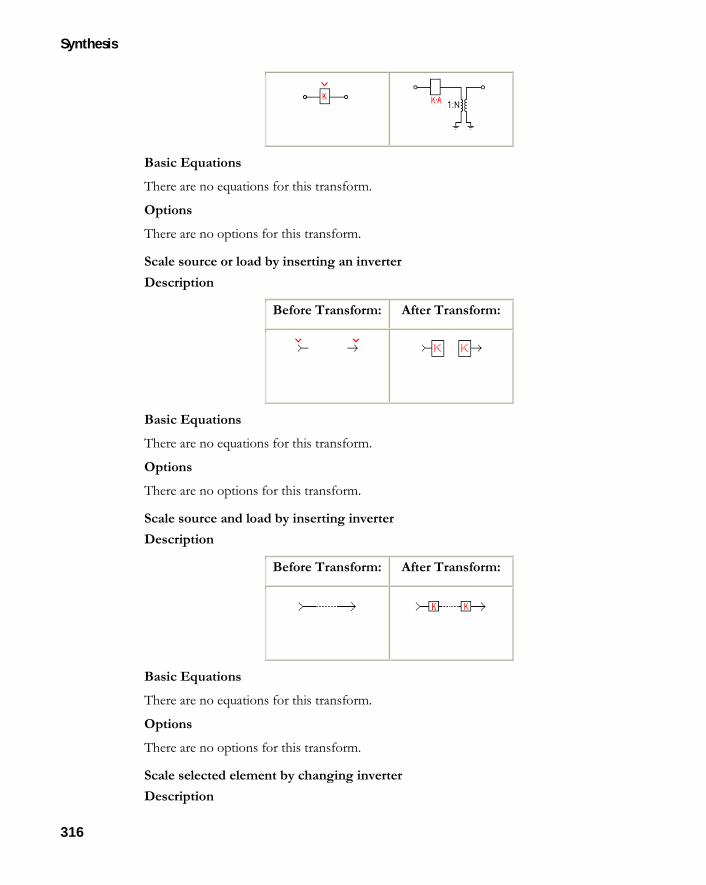
Synthesis
316
Basic Equations
There are no equations for this transform.
Options
There are no options for this transform.
Scale source or load by inserting an inverter Description
Before Transform: After Transform:
Basic Equations
There are no equations for this transform.
Options
There are no options for this transform.
Scale source and load by inserting inverter Description
Before Transform: After Transform:
Basic Equations
There are no equations for this transform.
Options
There are no options for this transform.
Scale selected element by changing inverter Description

S/FILTER
317
Before Transform: After Transform:
Basic Equations
There are no equations for this transform.
Options
There are no options for this transform.
Insert inverter before selected part Description
Before Transform: After Transform:
Basic Equations
There are no equations for this transform.
Options
There are no options for this transform.
Absorb adjacent transformer Description
Before Transform: After Transform:
Basic Equations
There are no equations for this transform.
Options
There are no options for this transform.
Pi to Inverter
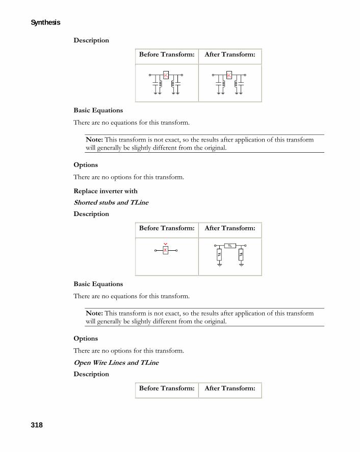
Synthesis
318
Description
Before Transform: After Transform:
Basic Equations
There are no equations for this transform.
Note: This transform is not exact, so the results after application of this transform will generally be slightly different from the original.
Options There are no options for this transform.
Replace inverter with Shorted stubs and TLine Description
Before Transform: After Transform:
Basic Equations
There are no equations for this transform.
Note: This transform is not exact, so the results after application of this transform will generally be slightly different from the original.
Options There are no options for this transform.
Open Wire Lines and TLine Description
Before Transform: After Transform:
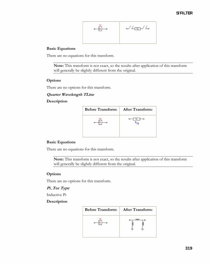
S/FILTER
319
Basic Equations
There are no equations for this transform.
Note: This transform is not exact, so the results after application of this transform will generally be slightly different from the original.
Options There are no options for this transform.
Quarter Wavelength TLine Description
Before Transform: After Transform:
Basic Equations
There are no equations for this transform.
Note: This transform is not exact, so the results after application of this transform will generally be slightly different from the original.
Options There are no options for this transform.
Pi_Tee Type Inductive Pi Description
Before Transform: After Transform:

Synthesis
320
Before Transform: After Transform:
Basic Equations
There are no equations for this transform.
Note: This transform is not exact, so the results after application of this transform will generally be slightly different from the original.
Options There are no options for this transform.
Capacitive Pi Description
Before Transform: After Transform:
Before Transform: After Transform:
Basic Equations
There are no equations for this transform.
Note: This transform is not exact, so the results after application of this transform will generally be slightly different from the original.
Options There are no options for this transform.
Inductive Tee Description
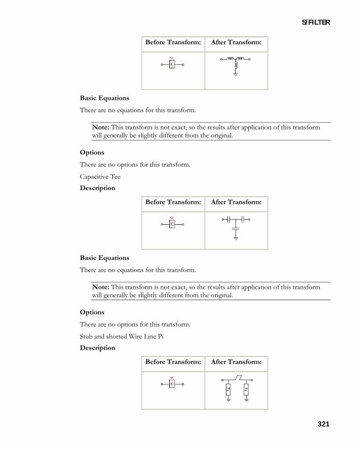
S/FILTER
321
Before Transform: After Transform:
Basic Equations
There are no equations for this transform.
Note: This transform is not exact, so the results after application of this transform will generally be slightly different from the original.
Options There are no options for this transform.
Capacitive Tee Description
Before Transform: After Transform:
Basic Equations
There are no equations for this transform.
Note: This transform is not exact, so the results after application of this transform will generally be slightly different from the original.
Options There are no options for this transform.
Stub and shorted Wire Line Pi Description
Before Transform: After Transform:
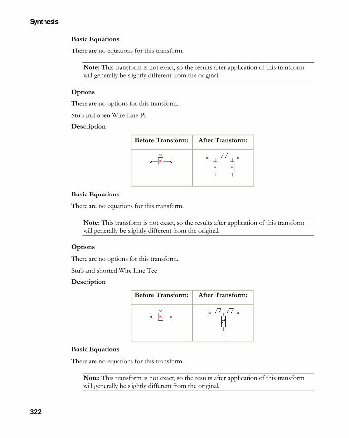
Synthesis
322
Basic Equations
There are no equations for this transform.
Note: This transform is not exact, so the results after application of this transform will generally be slightly different from the original.
Options There are no options for this transform.
Stub and open Wire Line Pi Description
Before Transform: After Transform:
Basic Equations
There are no equations for this transform.
Note: This transform is not exact, so the results after application of this transform will generally be slightly different from the original.
Options There are no options for this transform.
Stub and shorted Wire Line Tee Description
Before Transform: After Transform:
Basic Equations
There are no equations for this transform.
Note: This transform is not exact, so the results after application of this transform will generally be slightly different from the original.
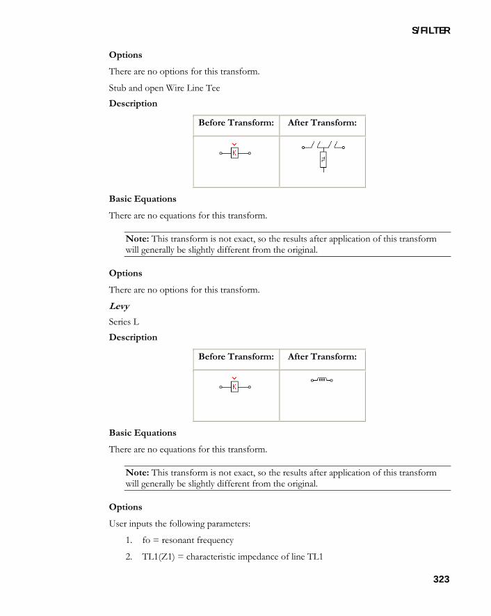
S/FILTER
323
Options There are no options for this transform.
Stub and open Wire Line Tee Description
Before Transform: After Transform:
Basic Equations
There are no equations for this transform.
Note: This transform is not exact, so the results after application of this transform will generally be slightly different from the original.
Options There are no options for this transform.
Levy Series L Description
Before Transform: After Transform:
Basic Equations
There are no equations for this transform.
Note: This transform is not exact, so the results after application of this transform will generally be slightly different from the original.
Options User inputs the following parameters:
1. fo = resonant frequency
2. TL1(Z1) = characteristic impedance of line TL1
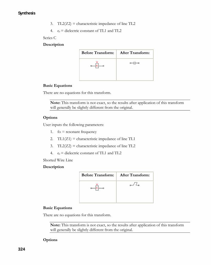
Synthesis
324
3. TL2(Z2) = characteristic impedance of line TL2
4. er = dielectric constant of TL1 and TL2
Series C Description
Before Transform: After Transform:
Basic Equations
There are no equations for this transform.
Note: This transform is not exact, so the results after application of this transform will generally be slightly different from the original.
Options User inputs the following parameters:
1. fo = resonant frequency
2. TL1(Z1) = characteristic impedance of line TL1
3. TL2(Z2) = characteristic impedance of line TL2
4. er = dielectric constant of TL1 and TL2
Shorted Wire Line Description
Before Transform: After Transform:
Basic Equations
There are no equations for this transform.
Note: This transform is not exact, so the results after application of this transform will generally be slightly different from the original.
Options
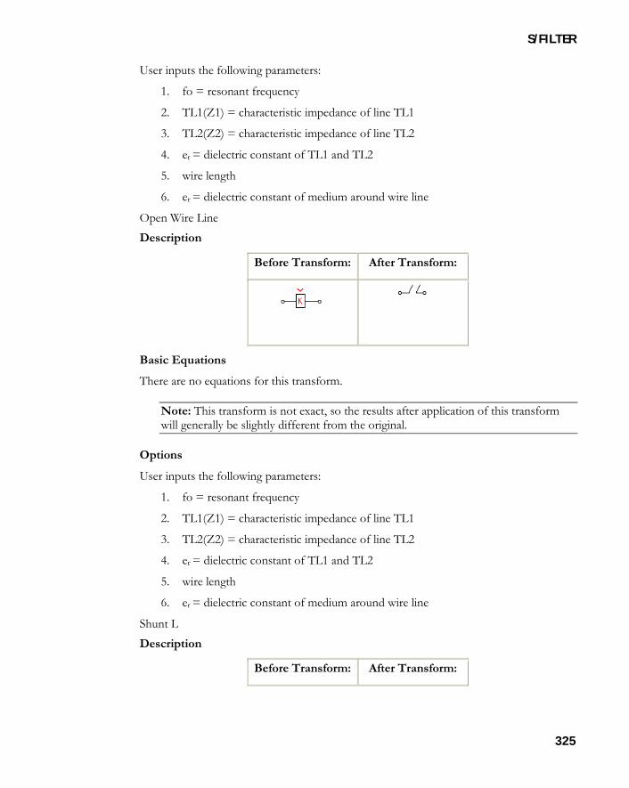
S/FILTER
325
User inputs the following parameters:
1. fo = resonant frequency
2. TL1(Z1) = characteristic impedance of line TL1
3. TL2(Z2) = characteristic impedance of line TL2
4. er = dielectric constant of TL1 and TL2
5. wire length
6. er = dielectric constant of medium around wire line
Open Wire Line Description
Before Transform: After Transform:
Basic Equations
There are no equations for this transform.
Note: This transform is not exact, so the results after application of this transform will generally be slightly different from the original.
Options User inputs the following parameters:
1. fo = resonant frequency
2. TL1(Z1) = characteristic impedance of line TL1
3. TL2(Z2) = characteristic impedance of line TL2
4. er = dielectric constant of TL1 and TL2
5. wire length
6. er = dielectric constant of medium around wire line
Shunt L Description
Before Transform: After Transform:
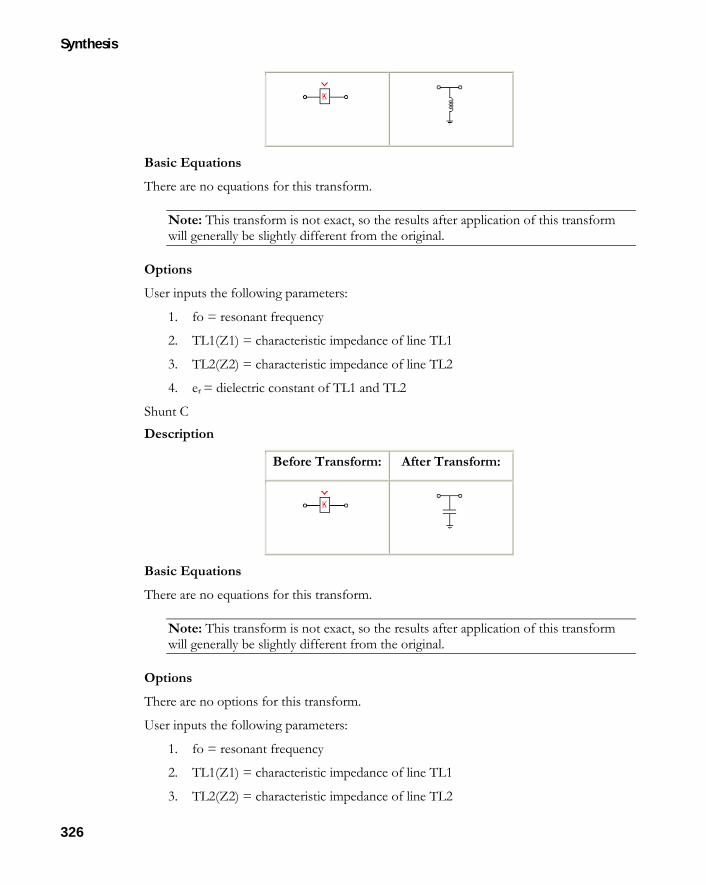
Synthesis
326
Basic Equations
There are no equations for this transform.
Note: This transform is not exact, so the results after application of this transform will generally be slightly different from the original.
Options User inputs the following parameters:
1. fo = resonant frequency
2. TL1(Z1) = characteristic impedance of line TL1
3. TL2(Z2) = characteristic impedance of line TL2
4. er = dielectric constant of TL1 and TL2
Shunt C Description
Before Transform: After Transform:
Basic Equations
There are no equations for this transform.
Note: This transform is not exact, so the results after application of this transform will generally be slightly different from the original.
Options There are no options for this transform.
User inputs the following parameters:
1. fo = resonant frequency
2. TL1(Z1) = characteristic impedance of line TL1
3. TL2(Z2) = characteristic impedance of line TL2
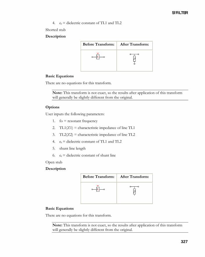
S/FILTER
327
4. er = dielectric constant of TL1 and TL2
Shorted stub Description
Before Transform: After Transform:
Basic Equations
There are no equations for this transform.
Note: This transform is not exact, so the results after application of this transform will generally be slightly different from the original.
Options User inputs the following parameters:
1. fo = resonant frequency
2. TL1(Z1) = characteristic impedance of line TL1
3. TL2(Z2) = characteristic impedance of line TL2
4. er = dielectric constant of TL1 and TL2
5. shunt line length
6. er = dielectric constant of shunt line
Open stub Description
Before Transform: After Transform:
Basic Equations
There are no equations for this transform.
Note: This transform is not exact, so the results after application of this transform will generally be slightly different from the original.
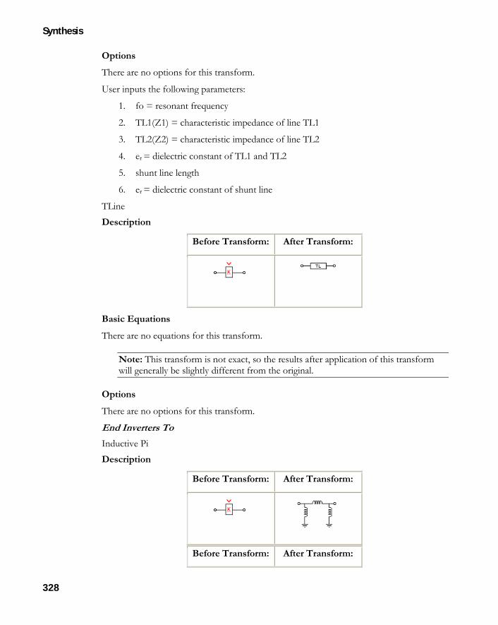
Synthesis
328
Options There are no options for this transform.
User inputs the following parameters:
1. fo = resonant frequency
2. TL1(Z1) = characteristic impedance of line TL1
3. TL2(Z2) = characteristic impedance of line TL2
4. er = dielectric constant of TL1 and TL2
5. shunt line length
6. er = dielectric constant of shunt line
TLine Description
Before Transform: After Transform:
Basic Equations
There are no equations for this transform.
Note: This transform is not exact, so the results after application of this transform will generally be slightly different from the original.
Options There are no options for this transform.
End Inverters To Inductive Pi Description
Before Transform: After Transform:
Before Transform: After Transform:
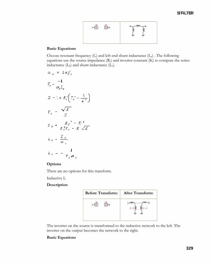
S/FILTER
329
Basic Equations
Choose resonant frequency (fo) and left end shunt inductance (La) . The following equations use the source impedance (Rs) and inverter constant (K) to compute the series inductance (Lb) and shunt inductance (Lc).
Options
There are no options for this transform.
Inductive L Description
Before Transform: After Transform:
The inverter on the source is transformed to the inductive network to the left. The inverter on the output becomes the network to the right.
Basic Equations
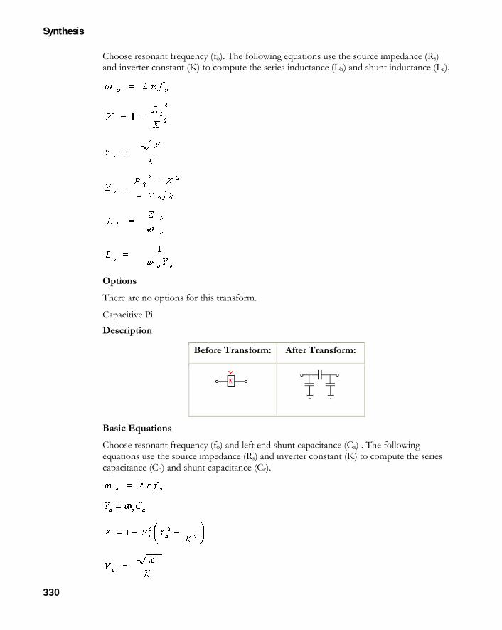
Synthesis
330
Choose resonant frequency (fo). The following equations use the source impedance (Rs) and inverter constant (K) to compute the series inductance (Lb) and shunt inductance (Lc).
Options
There are no options for this transform.
Capacitive Pi Description
Before Transform: After Transform:
Basic Equations
Choose resonant frequency (fo) and left end shunt capacitance (Ca) . The following equations use the source impedance (Rs) and inverter constant (K) to compute the series capacitance (Cb) and shunt capacitance (Cc).
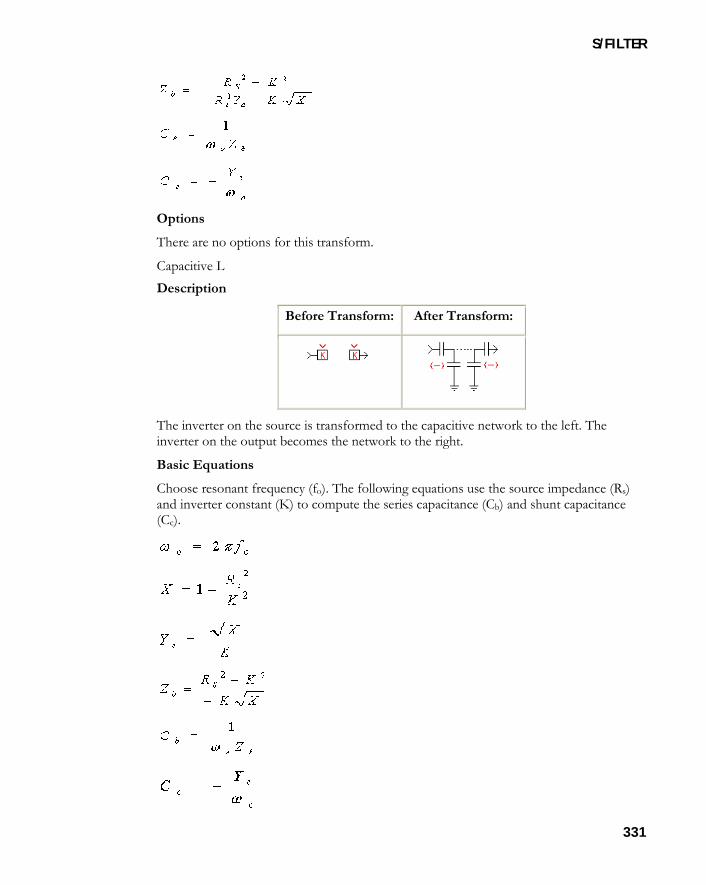
S/FILTER
331
Options
There are no options for this transform.
Capacitive L Description
Before Transform: After Transform:
The inverter on the source is transformed to the capacitive network to the left. The inverter on the output becomes the network to the right.
Basic Equations
Choose resonant frequency (fo). The following equations use the source impedance (Rs) and inverter constant (K) to compute the series capacitance (Cb) and shunt capacitance (Cc).
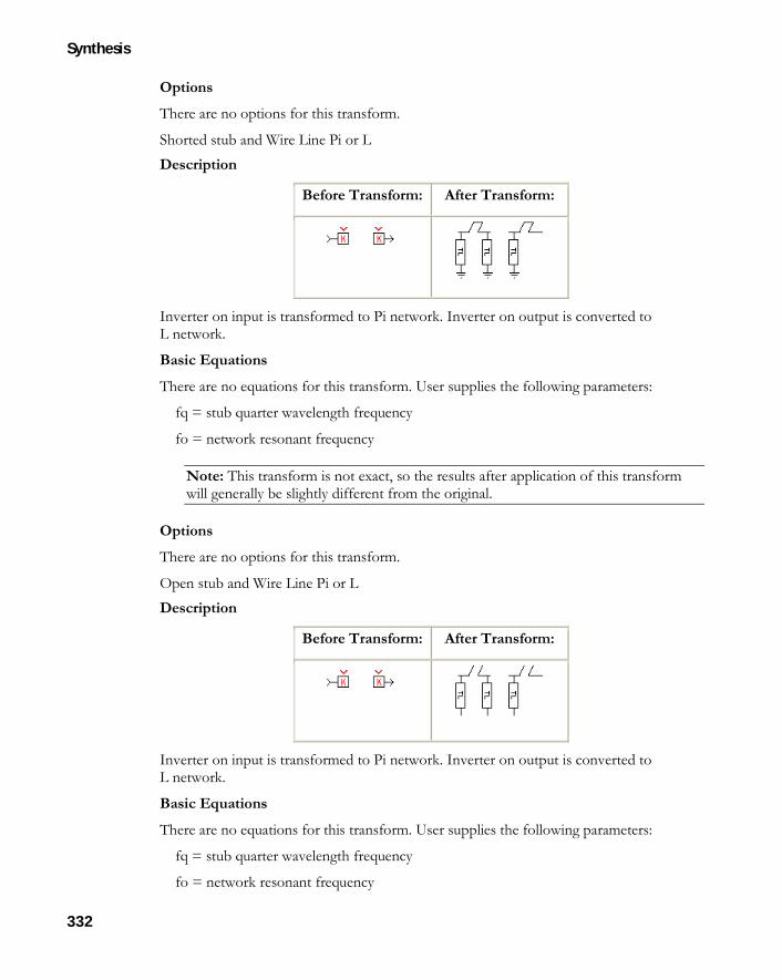
Synthesis
332
Options
There are no options for this transform.
Shorted stub and Wire Line Pi or L Description
Before Transform: After Transform:
Inverter on input is transformed to Pi network. Inverter on output is converted to L network.
Basic Equations
There are no equations for this transform. User supplies the following parameters:
fq = stub quarter wavelength frequency
fo = network resonant frequency
Note: This transform is not exact, so the results after application of this transform will generally be slightly different from the original.
Options There are no options for this transform.
Open stub and Wire Line Pi or L Description
Before Transform: After Transform:
Inverter on input is transformed to Pi network. Inverter on output is converted to L network.
Basic Equations
There are no equations for this transform. User supplies the following parameters:
fq = stub quarter wavelength frequency
fo = network resonant frequency
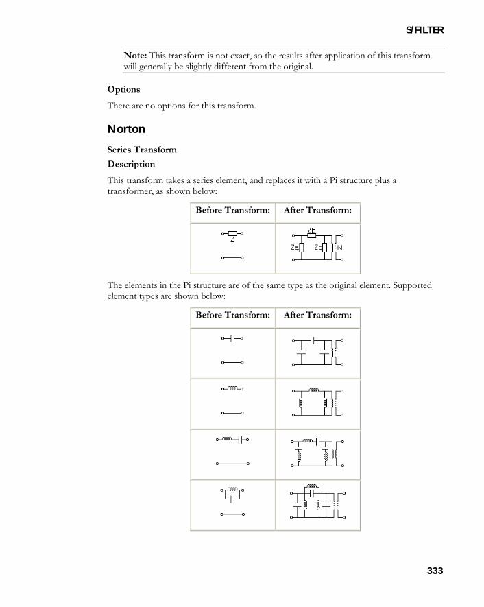
S/FILTER
333
Note: This transform is not exact, so the results after application of this transform will generally be slightly different from the original.
Options There are no options for this transform.
Norton
Series Transform Description
This transform takes a series element, and replaces it with a Pi structure plus a transformer, as shown below:
Before Transform: After Transform:
The elements in the Pi structure are of the same type as the original element. Supported element types are shown below:
Before Transform: After Transform:

Synthesis
334
Note: When using this transform on a series resonator in series, both elements within the resonator must be selected. Otherwise, a single element transform is applied.
Example
In this example, the transformer ratio is chosen as 4.
Basic Equations
The basic equations for the Norton Series Transform are shown below:
Options
Options available for this transform are:
Specify Left (Za) Specifying Za causes S/FILTER to calculate the transformer ratio using the following equation:
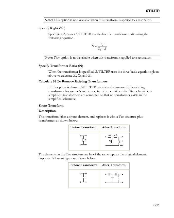
S/FILTER
335
Note: This option is not available when this transform is applied to a resonator.
Specify Right (Zc) Specifying Zc causes S/FILTER to calculate the transformer ratio using the following equation:
Note: This option is not available when this transform is applied to a resonator.
Specify Transformer Ratio (N) When the transformer is specified, S/FILTER uses the three basic equations given above to calculate Za, Zb, and Zc.
Calculate N To Remove Existing Transformers
If this option is chosen, S/FILTER calculates the inverse of the existing transformer for use as N in the new transformer. When the filter schematic is simplified, transformers are combined so that no transformer exists in the simplified schematic.
Shunt Transform Description
This transform takes a shunt element, and replaces it with a Tee structure plus transformer, as shown below:
Before Transform: After Transform:
The elements in the Tee structure are be of the same type as the original element. Supported element types are shown below:
Before Transform: After Transform:
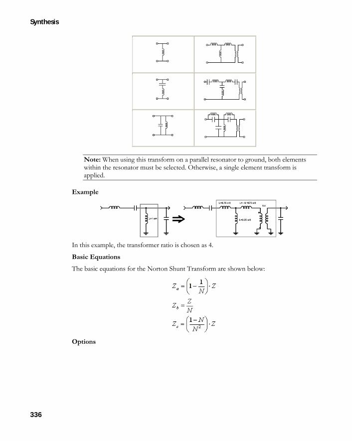
Synthesis
336
Note: When using this transform on a parallel resonator to ground, both elements within the resonator must be selected. Otherwise, a single element transform is applied.
Example
In this example, the transformer ratio is chosen as 4.
Basic Equations
The basic equations for the Norton Shunt Transform are shown below:
Options

S/FILTER
337
Options available for this transform are:
Choose The Left Element (Za) Specifying Za causes S/FILTER to calculate the transformer ratio using the following equation:
Note: This option is not available when this transform is applied to a resonator.
Choose The Right Element (Zc) Specifying Zc causes S/FILTER to calculate the transformer ratio using the following equation:
Note: This option is not available when this transform is applied to a resonator.
Choose The Transformer Ratio (N) When the transformer is specified, S/FILTER uses the three basic equations given above to calculate Za, Zb, and Zc.
Calculate N To Remove Existing Transformer(s) If this option is chosen, S/FILTER calculates the inverse of the existing transformer and use that as N for the new transformer. This causes the transformers to cancel each other when the filter schematic is simplified so that no transformer exists in the resulting schematic.
Scale Series Element Of Pi Description
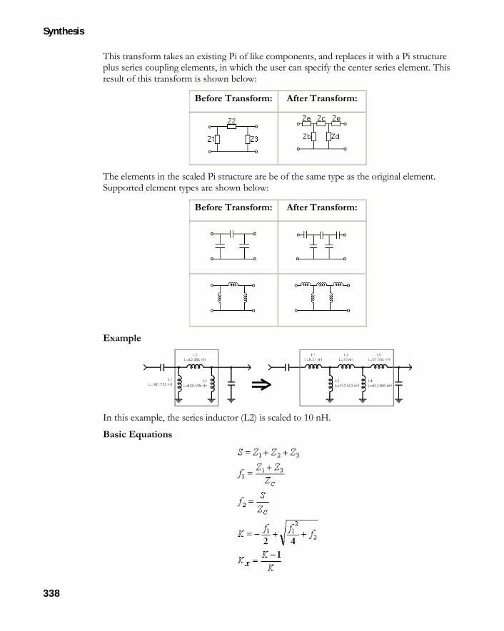
Synthesis
338
This transform takes an existing Pi of like components, and replaces it with a Pi structure plus series coupling elements, in which the user can specify the center series element. This result of this transform is shown below:
Before Transform: After Transform:
The elements in the scaled Pi structure are be of the same type as the original element. Supported element types are shown below:
Before Transform: After Transform:
Example
In this example, the series inductor (L2) is scaled to 10 nH.
Basic Equations
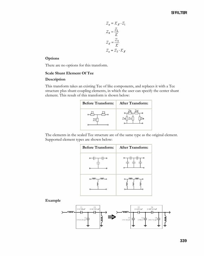
S/FILTER
339
Options
There are no options for this transform.
Scale Shunt Element Of Tee Description
This transform takes an existing Tee of like components, and replaces it with a Tee structure plus shunt coupling elements, in which the user can specify the center shunt element. This result of this transform is shown below:
Before Transform: After Transform:
The elements in the scaled Tee structure are of the same type as the original element. Supported element types are shown below:
Before Transform: After Transform:
Example

Synthesis
340
In this example, the shunt capacitor (C2) is scaled to 50 pF.
Basic Equations
The equations for the Norton Scale Series Element of Pi Transform are shown below:
Options
There are no options for this transform.
Double Norton Colin parallel transform left Description
Before Transform: After Transform:
Basic Equations
There are no equations for this transform.
Options
There are no options for this transform.
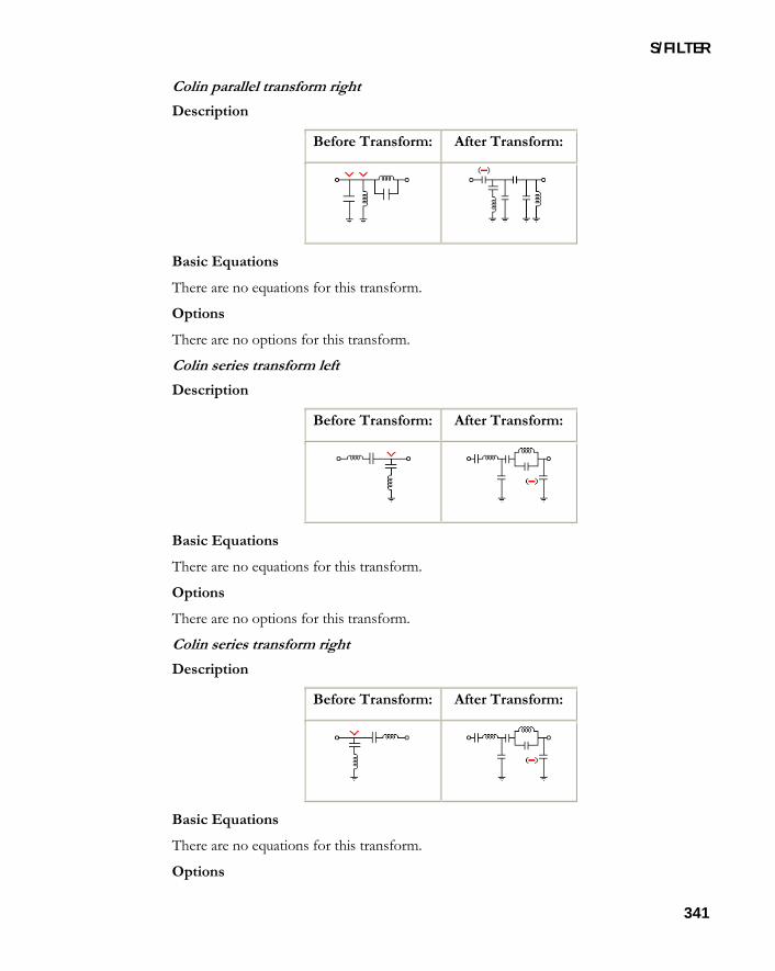
S/FILTER
341
Colin parallel transform right Description
Before Transform: After Transform:
Basic Equations
There are no equations for this transform.
Options
There are no options for this transform.
Colin series transform left Description
Before Transform: After Transform:
Basic Equations
There are no equations for this transform.
Options
There are no options for this transform.
Colin series transform right Description
Before Transform: After Transform:
Basic Equations
There are no equations for this transform.
Options
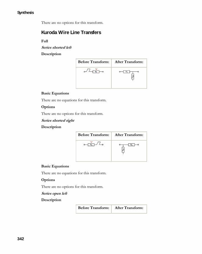
Synthesis
342
There are no options for this transform.
Kuroda Wire Line Transfers
Full Series shorted left Description
Before Transform: After Transform:
Basic Equations
There are no equations for this transform.
Options
There are no options for this transform.
Series shorted right Description
Before Transform: After Transform:
Basic Equations
There are no equations for this transform.
Options
There are no options for this transform.
Series open left Description
Before Transform: After Transform:

S/FILTER
343
Basic Equations
There are no equations for this transform.
Options
There are no options for this transform.
Series open right Description
Before Transform: After Transform:
Basic Equations
There are no equations for this transform.
Options
There are no options for this transform.
Shunt grounded left Description
Before Transform: After Transform:
Basic Equations
There are no equations for this transform.
Options
There are no options for this transform.
Shunt grounded right Description

Synthesis
344
Before Transform: After Transform:
Basic Equations
There are no equations for this transform.
Options
There are no options for this transform.
Shunt open left Description
Before Transform: After Transform:
Basic Equations
There are no equations for this transform.
Options
There are no options for this transform.
Shunt open right Description
Before Transform: After Transform:
Basic Equations
There are no equations for this transform.
Options
There are no options for this transform.
Minnis
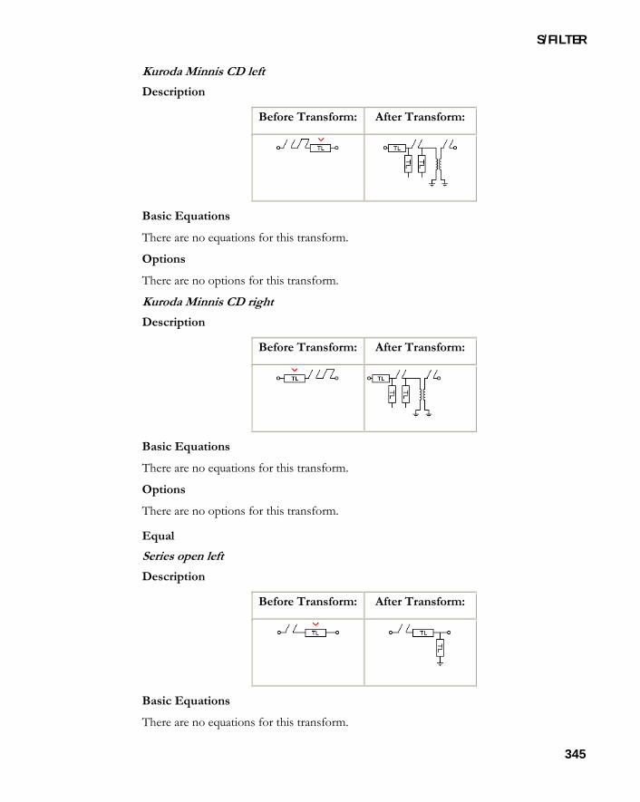
S/FILTER
345
Kuroda Minnis CD left Description
Before Transform: After Transform:
Basic Equations
There are no equations for this transform.
Options
There are no options for this transform.
Kuroda Minnis CD right Description
Before Transform: After Transform:
Basic Equations
There are no equations for this transform.
Options
There are no options for this transform.
Equal Series open left Description
Before Transform: After Transform:
Basic Equations
There are no equations for this transform.

Synthesis
346
Options
There are no options for this transform.
Series open right Description
Before Transform: After Transform:
Basic Equations
There are no equations for this transform.
Options
There are no options for this transform.
Shunt grounded left Description
Before Transform: After Transform:
Basic Equations
There are no equations for this transform.
Options
There are no options for this transform.
Shunt grounded right Description
Before Transform: After Transform:
Basic Equations

S/FILTER
347
There are no equations for this transform.
Options
There are no options for this transform.
Specify Transformer Series open left Description
Before Transform: After Transform:
Basic Equations
There are no equations for this transform.
Options
There are no options for this transform.
Series open right Description
Before Transform: After Transform:
Basic Equations
There are no equations for this transform.
Options
There are no options for this transform.
Shunt shorted left Description
Before Transform: After Transform:
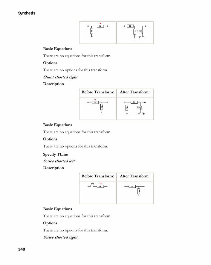
Synthesis
348
Basic Equations
There are no equations for this transform.
Options
There are no options for this transform.
Shunt shorted right Description
Before Transform: After Transform:
Basic Equations
There are no equations for this transform.
Options
There are no options for this transform.
Specify TLine Series shorted left Description
Before Transform: After Transform:
Basic Equations
There are no equations for this transform.
Options
There are no options for this transform.
Series shorted right

S/FILTER
349
Description
Before Transform: After Transform:
Basic Equations
There are no equations for this transform.
Options
There are no options for this transform.
Series open left Description
Before Transform: After Transform:
Basic Equations
There are no equations for this transform.
Options
There are no options for this transform.
Series open right Description
Before Transform: After Transform:
Basic Equations
There are no equations for this transform.
Options
There are no options for this transform.
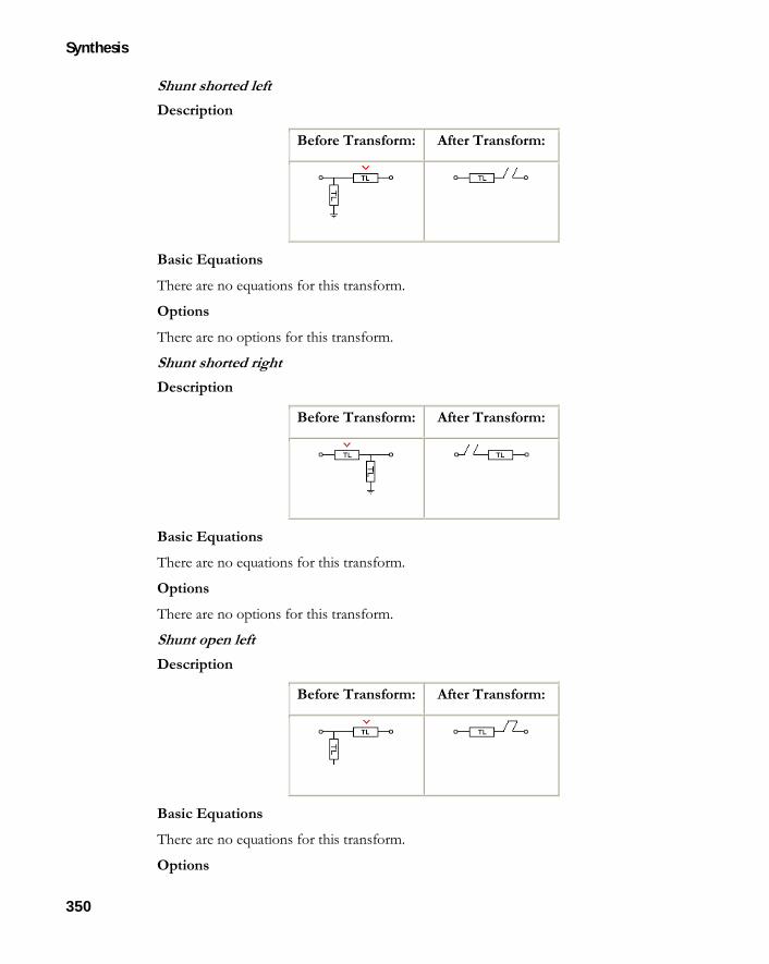
Synthesis
350
Shunt shorted left Description
Before Transform: After Transform:
Basic Equations
There are no equations for this transform.
Options
There are no options for this transform.
Shunt shorted right Description
Before Transform: After Transform:
Basic Equations
There are no equations for this transform.
Options
There are no options for this transform.
Shunt open left Description
Before Transform: After Transform:
Basic Equations
There are no equations for this transform.
Options
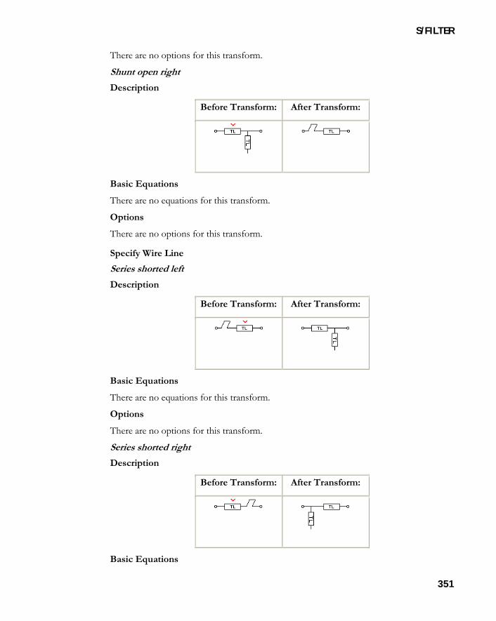
S/FILTER
351
There are no options for this transform.
Shunt open right Description
Before Transform: After Transform:
Basic Equations
There are no equations for this transform.
Options
There are no options for this transform.
Specify Wire Line Series shorted left Description
Before Transform: After Transform:
Basic Equations
There are no equations for this transform.
Options
There are no options for this transform.
Series shorted right Description
Before Transform: After Transform:
Basic Equations
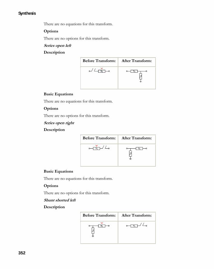
Synthesis
352
There are no equations for this transform.
Options
There are no options for this transform.
Series open left Description
Before Transform: After Transform:
Basic Equations
There are no equations for this transform.
Options
There are no options for this transform.
Series open right Description
Before Transform: After Transform:
Basic Equations
There are no equations for this transform.
Options
There are no options for this transform.
Shunt shorted left Description
Before Transform: After Transform:
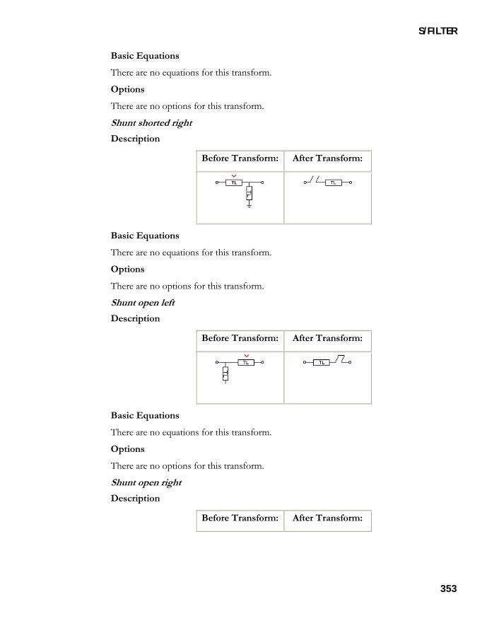
S/FILTER
353
Basic Equations
There are no equations for this transform.
Options
There are no options for this transform.
Shunt shorted right Description
Before Transform: After Transform:
Basic Equations
There are no equations for this transform.
Options
There are no options for this transform.
Shunt open left Description
Before Transform: After Transform:
Basic Equations
There are no equations for this transform.
Options
There are no options for this transform.
Shunt open right Description
Before Transform: After Transform:
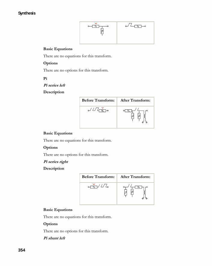
Synthesis
354
Basic Equations
There are no equations for this transform.
Options
There are no options for this transform.
Pi Pi series left Description
Before Transform: After Transform:
Basic Equations
There are no equations for this transform.
Options
There are no options for this transform.
Pi series right Description
Before Transform: After Transform:
Basic Equations
There are no equations for this transform.
Options
There are no options for this transform.
Pi shunt left
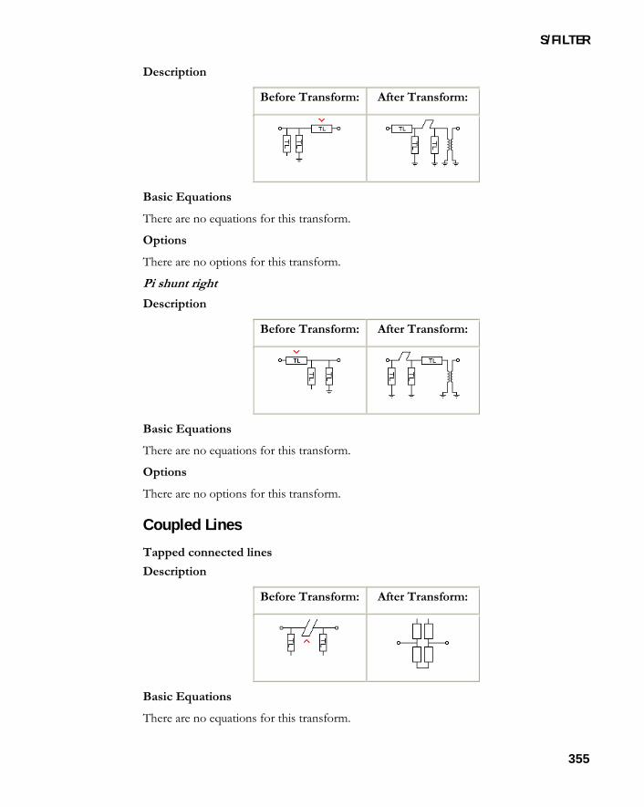
S/FILTER
355
Description
Before Transform: After Transform:
Basic Equations
There are no equations for this transform.
Options
There are no options for this transform.
Pi shunt right Description
Before Transform: After Transform:
Basic Equations
There are no equations for this transform.
Options
There are no options for this transform.
Coupled Lines
Tapped connected lines Description
Before Transform: After Transform:
Basic Equations
There are no equations for this transform.

Synthesis
356
Options
There are no options for this transform.
Homogeneous coupled lines to inhomogeneous Description
Before Transform: After Transform:
Basic Equations
There are no equations for this transform.
Options
There are no options for this transform.
2 TLines to tapped connc Wire Line eq. Description
Before Transform: After Transform:
Basic Equations
There are no equations for this transform.
Note: This transform is not exact, so the results after application of this transform will generally be slightly different from the original.
Options There are no options for this transform.
Comb lines Both lines grounded Description
This transform creates a pair of coupled lines as shown below:
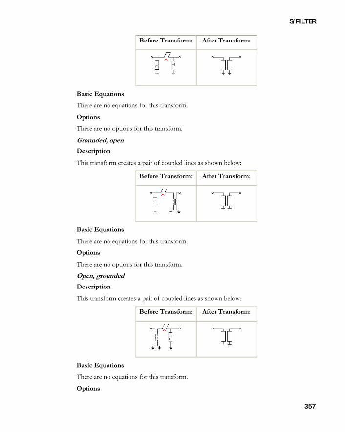
S/FILTER
357
Before Transform: After Transform:
Basic Equations
There are no equations for this transform.
Options
There are no options for this transform.
Grounded, open Description
This transform creates a pair of coupled lines as shown below:
Before Transform: After Transform:
Basic Equations
There are no equations for this transform.
Options
There are no options for this transform.
Open, grounded Description
This transform creates a pair of coupled lines as shown below:
Before Transform: After Transform:
Basic Equations
There are no equations for this transform.
Options
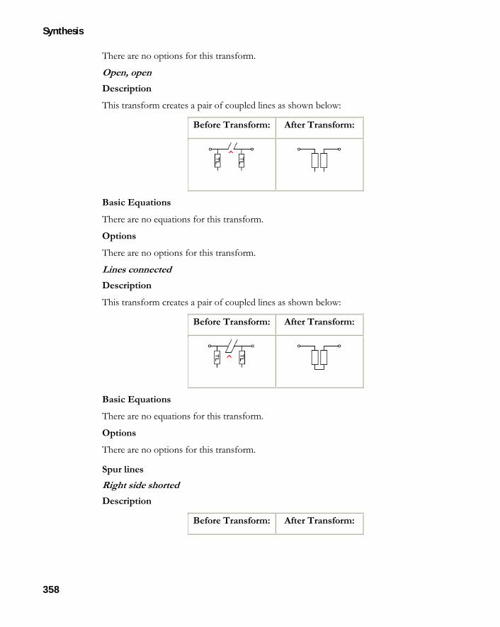
Synthesis
358
There are no options for this transform.
Open, open Description
This transform creates a pair of coupled lines as shown below:
Before Transform: After Transform:
Basic Equations
There are no equations for this transform.
Options
There are no options for this transform.
Lines connected Description
This transform creates a pair of coupled lines as shown below:
Before Transform: After Transform:
Basic Equations
There are no equations for this transform.
Options
There are no options for this transform.
Spur lines Right side shorted Description
Before Transform: After Transform:
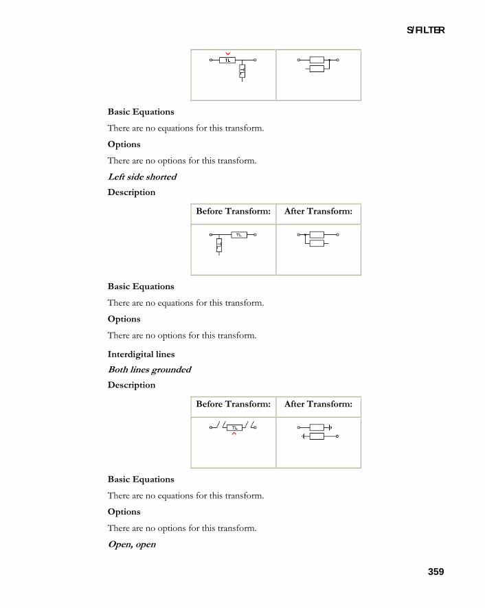
S/FILTER
359
Basic Equations
There are no equations for this transform.
Options
There are no options for this transform.
Left side shorted Description
Before Transform: After Transform:
Basic Equations
There are no equations for this transform.
Options
There are no options for this transform.
Interdigital lines Both lines grounded Description
Before Transform: After Transform:
Basic Equations
There are no equations for this transform.
Options
There are no options for this transform.
Open, open

Synthesis
360
Description
Before Transform: After Transform:
Basic Equations
There are no equations for this transform.
Options
There are no options for this transform.
Ikeno lines Both ends grounded Description
Before Transform: After Transform:
Basic Equations
There are no equations for this transform.
Note: This transform is not exact, so the results after application of this transform will generally be slightly different from the original.
Options There are no options for this transform.
Grounded, open Description
Before Transform: After Transform:

S/FILTER
361
Basic Equations
There are no equations for this transform.
Note: This transform is not exact, so the results after application of this transform will generally be slightly different from the original.
Options There are no options for this transform.
Open, grounded Description
Before Transform: After Transform:
Basic Equations
There are no equations for this transform.
Note: This transform is not exact, so the results after application of this transform will generally be slightly different from the original.
Options There are no options for this transform.
Open, open Description
Before Transform: After Transform:
Basic Equations
There are no equations for this transform.
Note: This transform is not exact, so the results after application of this transform will generally be slightly different from the original.
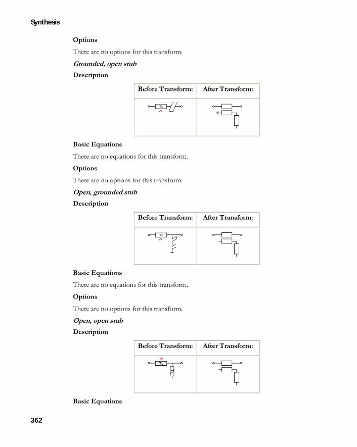
Synthesis
362
Options There are no options for this transform.
Grounded, open stub Description
Before Transform: After Transform:
Basic Equations
There are no equations for this transform.
Options
There are no options for this transform.
Open, grounded stub Description
Before Transform: After Transform:
Basic Equations
There are no equations for this transform.
Options
There are no options for this transform.
Open, open stub Description
Before Transform: After Transform:
Basic Equations

S/FILTER
363
There are no equations for this transform.
Options
There are no options for this transform.
Grounded stub, open Description
Before Transform: After Transform:
Basic Equations
There are no equations for this transform.
Options
There are no options for this transform.
Open stub, grounded Description
Before Transform: After Transform:
Basic Equations
There are no equations for this transform.
Options
There are no options for this transform.
Open stub, open Description
Before Transform: After Transform:
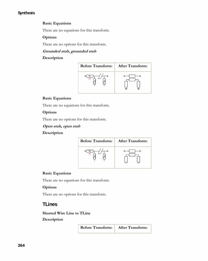
Synthesis
364
Basic Equations
There are no equations for this transform.
Options
There are no options for this transform.
Grounded stub, grounded stub Description
Before Transform: After Transform:
Basic Equations
There are no equations for this transform.
Options
There are no options for this transform.
Open stub, open stub Description
Before Transform: After Transform:
Basic Equations
There are no equations for this transform.
Options
There are no options for this transform.
TLines
Shorted Wire Line to TLine Description
Before Transform: After Transform:

S/FILTER
365
Basic Equations
There are no equations for this transform.
Note: This transform is not exact, so the results after application of this transform will generally be slightly different from the original.
Options There are no options for this transform.
Open stub to TLine Description
Before Transform: After Transform:
Basic Equations
There are no equations for this transform.
Note: This transform is not exact, so the results after application of this transform will generally be slightly different from the original.
Options There are no options for this transform.
Replace TLine Wire Line Tee Description
Before Transform: After Transform:

Synthesis
366
Basic Equations
There are no equations for this transform.
Note: This transform is not exact, so the results after application of this transform will generally be slightly different from the original.
Options There are no options for this transform.
Wire Line and capacitive Tee Description
Before Transform: After Transform:
Basic Equations
There are no equations for this transform.
Note: This transform is not exact, so the results after application of this transform will generally be slightly different from the original.
Options There are no options for this transform.
Stub and Wire Line Pi Description
Before Transform: After Transform:
Basic Equations
There are no equations for this transform.
Note: This transform is not exact, so the results after application of this transform will generally be slightly different from the original.
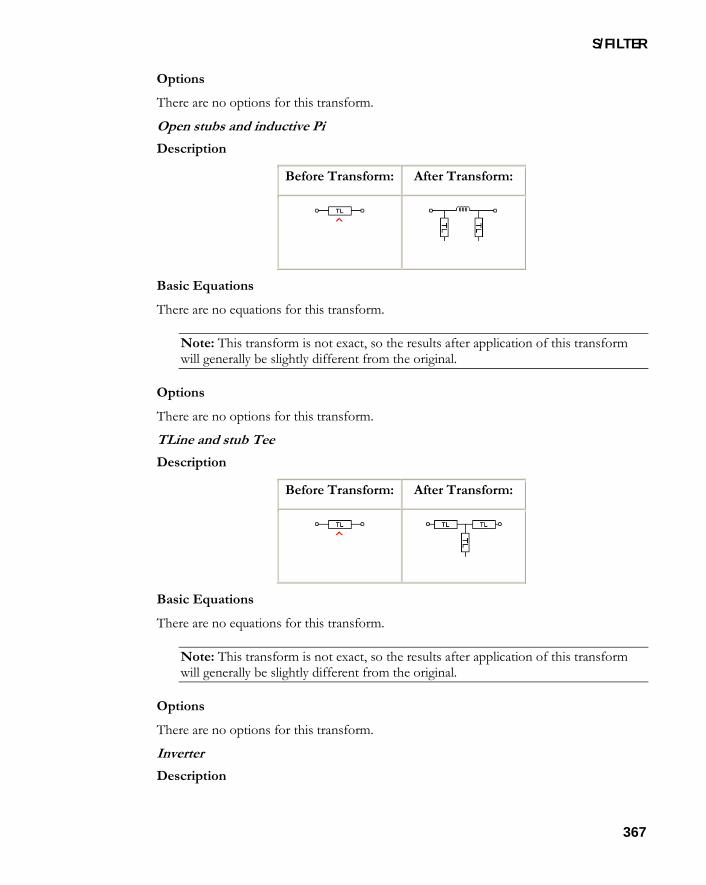
S/FILTER
367
Options There are no options for this transform.
Open stubs and inductive Pi Description
Before Transform: After Transform:
Basic Equations
There are no equations for this transform.
Note: This transform is not exact, so the results after application of this transform will generally be slightly different from the original.
Options There are no options for this transform.
TLine and stub Tee Description
Before Transform: After Transform:
Basic Equations
There are no equations for this transform.
Note: This transform is not exact, so the results after application of this transform will generally be slightly different from the original.
Options There are no options for this transform.
Inverter Description

Synthesis
368
Before Transform: After Transform:
Basic Equations
There are no equations for this transform.
Note: This transform is not exact, so the results after application of this transform will generally be slightly different from the original.
Options There are no options for this transform.
Scaled down TLine and Wire Lines Description
Before Transform: After Transform:
Basic Equations
There are no equations for this transform.
Note: This transform is not exact, so the results after application of this transform will generally be slightly different from the original.
Options There are no options for this transform.
Scaled up TLine and stubs Description
Before Transform: After Transform:
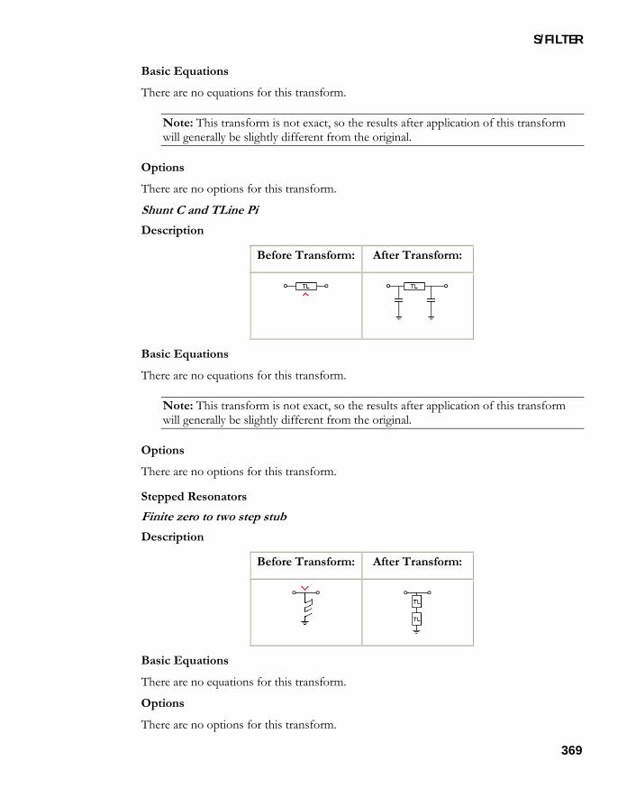
S/FILTER
369
Basic Equations
There are no equations for this transform.
Note: This transform is not exact, so the results after application of this transform will generally be slightly different from the original.
Options There are no options for this transform.
Shunt C and TLine Pi Description
Before Transform: After Transform:
Basic Equations
There are no equations for this transform.
Note: This transform is not exact, so the results after application of this transform will generally be slightly different from the original.
Options There are no options for this transform.
Stepped Resonators Finite zero to two step stub Description
Before Transform: After Transform:
Basic Equations
There are no equations for this transform.
Options
There are no options for this transform.
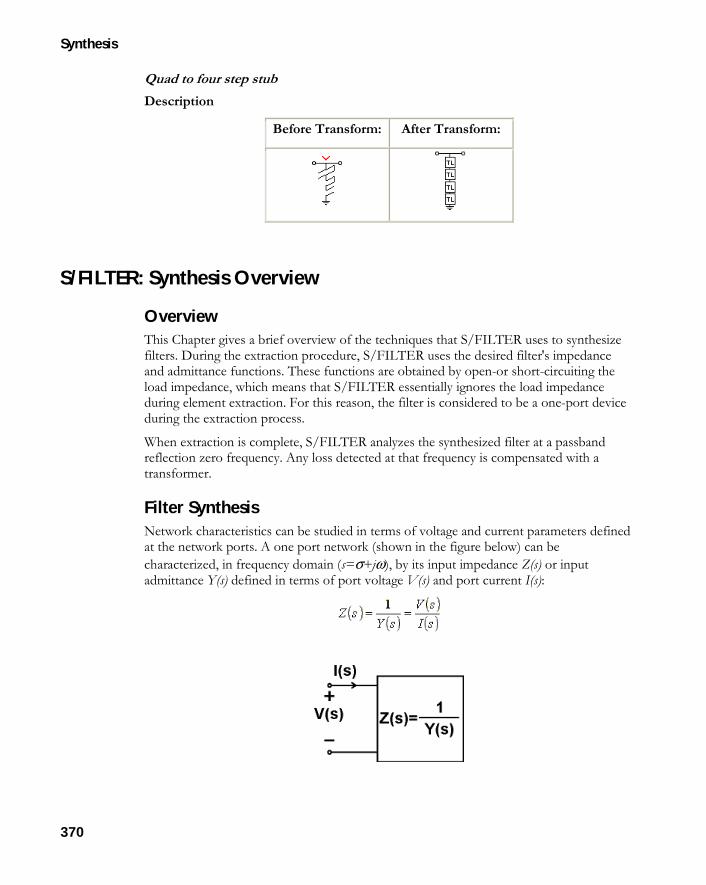
Synthesis
370
Quad to four step stub Description
Before Transform: After Transform:
S/FILTER: Synthesis Overview
Overview This Chapter gives a brief overview of the techniques that S/FILTER uses to synthesize filters. During the extraction procedure, S/FILTER uses the desired filter's impedance and admittance functions. These functions are obtained by open-or short-circuiting the load impedance, which means that S/FILTER essentially ignores the load impedance during element extraction. For this reason, the filter is considered to be a one-port device during the extraction process.
When extraction is complete, S/FILTER analyzes the synthesized filter at a passband reflection zero frequency. Any loss detected at that frequency is compensated with a transformer.
Filter Synthesis Network characteristics can be studied in terms of voltage and current parameters defined at the network ports. A one port network (shown in the figure below) can be characterized, in frequency domain (s=σ+jω), by its input impedance Z(s) or input admittance Y(s) defined in terms of port voltage V(s) and port current I(s):

S/FILTER
371
Analytical properties of input immittances of passive, lossless one ports are of fundamental importance in the synthesis of filters since S/FILTER alternately uses both Z(s) and Y(s) in the extraction procedure.
Some basic properties of these immitance functions are summarized below:
Driving point impedance Z(s) (and Y(s)) of a linear, time invariant, passive and lumped one-port is a positive real function:
1. Z(s) is real for "s" real
2. Re[Z(s)]>0 for Re[s]> 0
This theorem establishes both necessary and sufficient conditions for realizability of a given Z(s) (or Y(s)). These properties affect the polynomials forming Z(s) as follows:
Let
Then:
1. N(s) and D(s) are Hurwitz polynomials (i.e. they have no roots in the right half of the s=σ+jω plane).
2. The roots on the s=jω axis, including those at s=0 and s=∞, if they exist, must have unit multiplicity with positive residues.
3. Condition 2 implies that the degrees of N(s) and D(s) may differ at most by unity.
Foster's Reactance Theorem further details some properties of lossless networks (networks consisting of pure reactances):
Foster's Reactance Theorem For a positive real rational function Z(s)=1/Y(s) to be realizable as the driving point impedance of a lossless one-port, the necessary and sufficient condition is that it should be expressible in the form
where an and bm are constants and
1. 0 ≤ w1 < w2 < w3 (Interlacing poles and zeros, all on jω axis)
2. Foster's Theorem further restricts the degrees of the numerator, n, and denominator, m, by requiring that they must differ by unity. In other words, if the numerator is an even degree, the denominator is odd, and vice versa.
From these conditions, the following properties can be deduced:
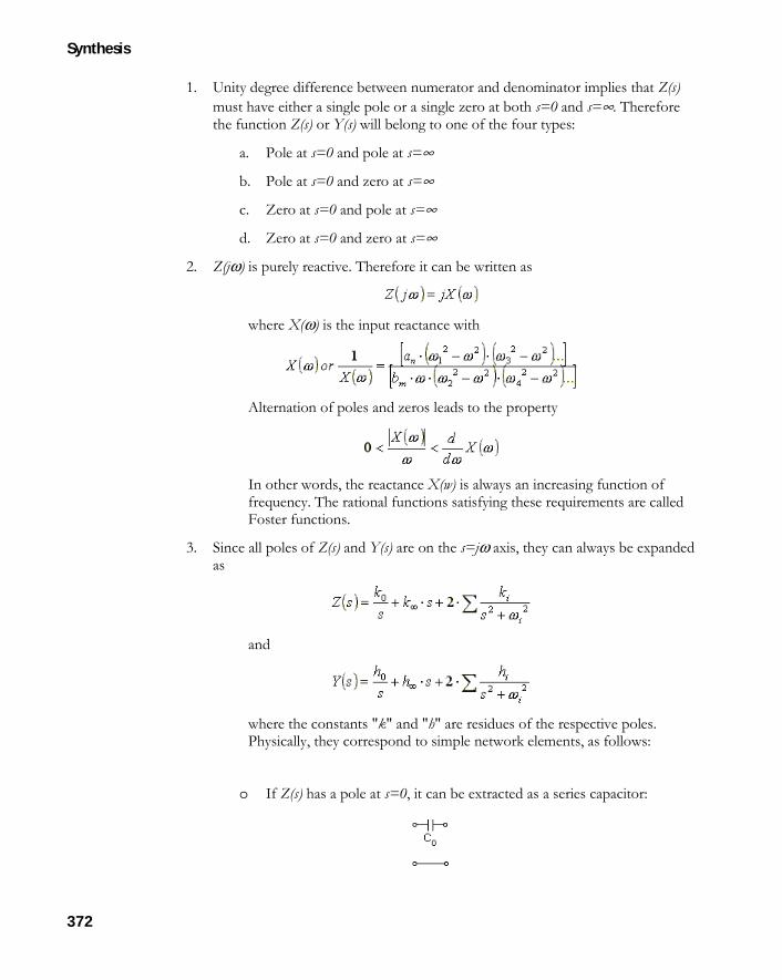
Synthesis
372
1. Unity degree difference between numerator and denominator implies that Z(s) must have either a single pole or a single zero at both s=0 and s=∞. Therefore the function Z(s) or Y(s) will belong to one of the four types:
a. Pole at s=0 and pole at s=∞
b. Pole at s=0 and zero at s=∞
c. Zero at s=0 and pole at s=∞
d. Zero at s=0 and zero at s=∞
2. Z(jω) is purely reactive. Therefore it can be written as
where X(ω) is the input reactance with
Alternation of poles and zeros leads to the property
In other words, the reactance X(w) is always an increasing function of frequency. The rational functions satisfying these requirements are called Foster functions.
3. Since all poles of Z(s) and Y(s) are on the s=jω axis, they can always be expanded as
and
where the constants "k" and "h" are residues of the respective poles. Physically, they correspond to simple network elements, as follows:
o If Z(s) has a pole at s=0, it can be extracted as a series capacitor:

S/FILTER
373
o If Z(s) has a pole at s=∞, it can be extracted as a series inductor:
o If Z(s) has a pole at s=jωi, it can be extracted as a parallel resonator in
series:
o If Y(s) has a pole at s=0, it can be extracted as a shunt inductor:
o If Y(s) has a pole at s=∞, it can be extracted as a shunt capacitor:
o If Y(s) has a pole at s=jωi, it can be extracted as a series resonator to
ground:
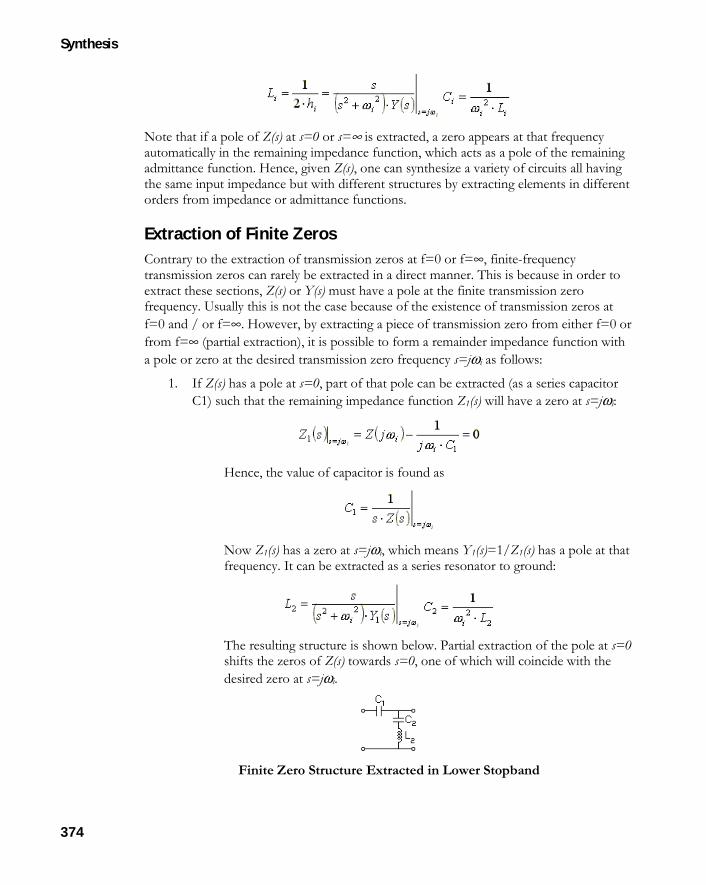
Synthesis
374
Note that if a pole of Z(s) at s=0 or s=∞ is extracted, a zero appears at that frequency automatically in the remaining impedance function, which acts as a pole of the remaining admittance function. Hence, given Z(s), one can synthesize a variety of circuits all having the same input impedance but with different structures by extracting elements in different orders from impedance or admittance functions.
Extraction of Finite Zeros Contrary to the extraction of transmission zeros at f=0 or f=∞, finite-frequency transmission zeros can rarely be extracted in a direct manner. This is because in order to extract these sections, Z(s) or Y(s) must have a pole at the finite transmission zero frequency. Usually this is not the case because of the existence of transmission zeros at f=0 and / or f=∞. However, by extracting a piece of transmission zero from either f=0 or from f=∞ (partial extraction), it is possible to form a remainder impedance function with a pole or zero at the desired transmission zero frequency s=jωi as follows:
1. If Z(s) has a pole at s=0, part of that pole can be extracted (as a series capacitor C1) such that the remaining impedance function Z1(s) will have a zero at s=jωi:
Hence, the value of capacitor is found as
Now Z1(s) has a zero at s=jωi, which means Y1(s)=1/Z1(s) has a pole at that frequency. It can be extracted as a series resonator to ground:
The resulting structure is shown below. Partial extraction of the pole at s=0 shifts the zeros of Z(s) towards s=0, one of which will coincide with the desired zero at s=jωi.
Finite Zero Structure Extracted in Lower Stopband
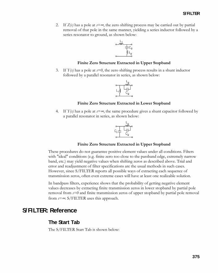
S/FILTER
375
2. If Z(s) has a pole at s=∞, the zero shifting process may be carried out by partial removal of that pole in the same manner, yielding a series inductor followed by a series resonator to ground, as shown below:
Finite Zero Structure Extracted in Upper Stopband
3. If Y(s) has a pole at s=0, the zero shifting process results in a shunt inductor followed by a parallel resonator in series, as shown below:
Finite Zero Structure Extracted in Lower Stopband
4. If Y(s) has a pole at s=∞, the same procedure gives a shunt capacitor followed by a parallel resonator in series, as shown below:
Finite Zero Structure Extracted in Upper Stopband
These procedures do not guarantee positive element values under all conditions. Filters with "ideal" conditions (e.g. finite zero too close to the passband edge, extremely narrow band, etc.) may yield negative values when shifting zeros as described above. Trial and error and readjustment of filter specifications are the usual methods in such cases. However, since S/FILTER reports all possible ways of extracting each sequence of transmission zeros, often even extreme cases will have at least one realizable solution.
In bandpass filters, experience shows that the probability of getting negative element values decreases by extracting finite transmission zeros in lower stopband by partial pole removal from s=0 and finite transmission zeros of upper stopband by partial pole removal from s=∞. S/FILTER uses this approach.
S/FILTER: Reference
The Start Tab The S/FILTER Start Tab is shown below:

Synthesis
376
New Filter - Starts with a new design. Save Settings - saves all S/FILTER prompts and settings for later use.
Note: You must use this option to permanently save S/FILTER settings. They are not saved in the workspace.
Load Settings - loads files saved with the Save Settings button.
Shape Wizard - opens the Shape Wizard dialog for designing classic filter shapes.
The Specifications Tab The S/FILTER Specifications Tab is shown below:
S/FILTER
377
Source (ohms) - the filter source impedance, specified in Ω.
Load (ohms) - the filter load impedance, specified in Ω.
[Lower] Cutoff (MHz) - for bandpass filters, specifies the lower passband edge. For lowpass and highpass filters, specifies the passband edge frequency.
Upper Cutoff (MHz) - for bandpass filters, specifies the upper passband edge. This prompt is disabled for lowpass and highpass filters.
Ripple (dB) - passband ripple in decibels.
Cutoff Att. (dB) - Also used as the attenuation at the specified cutoff frequencies.
Process (Lumped, Distributed) - Select LC or transmission line filter design.
Max Flat - designs a filter with no passband ripple. If this option is selected, the Ripple (dB) prompt specifies the attenuation at the specified cutoff frequencies.
Equiripple - designs a filter with passband ripple. If this option is selected, the Ripple (dB) prompt specifies the amount of passband ripple.
Type (Lowpass, Highpass, Bandpass) - designates the type of filter to be designed.
Rescale Plot - scales the S/FILTER plot to fit the current filter specifications. Scaling is based only on cutoff frequencies.
Capacitor Q, Inductor Q - Allows specification of quality factor for lumped components.
Zero Frequency (MHz) - this column in the Zero Table specifies the frequency for transmission zeros. The first row is reserved for DC transmission zeros. The second row is reserved for transmission zeros at infinite frequency. To specify a finite transmission zero, type the frequency of the zero into this column anywhere after the second row.
Quantity - designates the number of zeros located at the frequency specified in the adjacent table cell. Transmission zeros at DC are specified in the first row. The second row is reserved for transmission zeros at infinite frequency.
The Extractions Tab The S/FILTER Extractions Tab is shown below:

Synthesis
378
Total Permutations - the number of unique ways to arrange the transmission zeros. This number is calculated by the following equation:
In the above equation, N is the number of unique finite frequencies at which transmission zeros exist.
Unique Solutions Found - number of unique schematics found during calculation. This number updates during calculation as more solutions are found. Check the "% Completed" progress bar to see if calculation is complete. This number is not necessarily equal to Total Permutations. In some cases, two extraction sequences may be unique, but yield electrically equivalent schematics (e.g. the only difference is resonator element ordering). In these cases, S/FILTER only reports one occurrence of each solution.
Max Solutions To Display - controls the number of solutions displayed in the Solution Table. If this number is larger than the number of unique solutions for the filter being designed, all unique solutions will appear in the Solution Table. If Use Goals is selected and this number is less than the number of unique solutions, S/FILTER will uses the following procedure:
1. Suppose the Max Solutions To Display is set to N.
2. The first N solutions found are placed in the table.
3. All subsequent solutions are compared to the ones in the table.
4. If a new solution has a smaller error than one already in the table, the new solution replaces the old one.
5. When calculation is complete (i.e. when "% Completed" reaches 100%), the table contains the best N solutions.

S/FILTER
379
% Completed - indicates the percent of calculation that has completed. When this number reaches 100%, calculation is complete.
Allow Inexact - allow extractions that use illegal ordering of finite zeros. In many cases, this results in a poor filter response, which often requires tuning or optimization. See the Filter Design Concepts section for more information on inexact extractions. Rows shown in red in the solution table are inexact.
Series Element First - when selected, all schematics will have an element to ground closest to the source. If this option is unchecked, all schematics will have a series element connected to the source. The figures below illustrate the use of this option:
Series First: Shunt First:
Specify Perm - Allows selection of permutation by moving poles and zeros. This option is convenient for getting an exact permutation type.
Edit Perm - When Specify Perm is checked, allows changing the permutation selected.
Recalculate - clears the Solution Table and restarts calculation.
Use Goals - applies the user extraction goals to calculate an error function for each solution. See Max Solutions To Display above for a description of how solutions are added to the Solution Table.
Edit Goals - opens the S/FILTER Extraction Goals dialog. This button is only enabled when Use Goals is selected.
Customize Table - opens the Customize Permutation Table dialog.
Auto Fit Table - Resizes the table columns so that the Solution Table fits into the window.
Solution Table - contains the unique solutions. See Max Solutions To Display above for a description of how solutions are added to the Solution Table.
The Transforms Tab The Transforms tab is shown below:
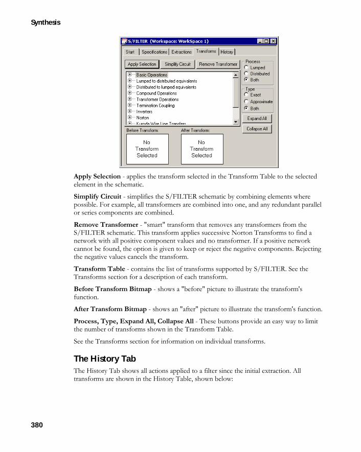
Synthesis
380
Apply Selection - applies the transform selected in the Transform Table to the selected element in the schematic.
Simplify Circuit - simplifies the S/FILTER schematic by combining elements where possible. For example, all transformers are combined into one, and any redundant parallel or series components are combined.
Remove Transformer - "smart" transform that removes any transformers from the S/FILTER schematic. This transform applies successive Norton Transforms to find a network with all positive component values and no transformer. If a positive network cannot be found, the option is given to keep or reject the negative components. Rejecting the negative values cancels the transform.
Transform Table - contains the list of transforms supported by S/FILTER. See the Transforms section for a description of each transform.
Before Transform Bitmap - shows a "before" picture to illustrate the transform's function.
After Transform Bitmap - shows an "after" picture to illustrate the transform's function.
Process, Type, Expand All, Collapse All - These buttons provide an easy way to limit the number of transforms shown in the Transform Table.
See the Transforms section for information on individual transforms.
The History Tab The History Tab shows all actions applied to a filter since the initial extraction. All transforms are shown in the History Table, shown below:

S/FILTER
381
The History Table is very similar to an "undo" list. By clicking any row in the table, the filter is returned to the state immediately after the item clicked. For example, in the figure above, row 5, "Simplify Schematic" is selected. The filter schematic reflects the filter state immediately after the schematic is simplified. Clicking row 4 would return the filter schematic to the state immediately after the Norton Shunt transform.
Whenever the filter design is changed (e.g. new cutoff frequencies, different topology), S/FILTER reapplies all actions listed in the History Table to the new filter. If any action fails as a result of the filter topology change, S/FILTER shows the failed actions in red. In the figure above, the Pi to Tee transform failed, so all transforms after and including the failed transform are marked in red.
Edit Selected - Edits the selected action. Some actions do not have any editable options (e.g. Simplify Schematic).
Delete Selected - Deletes the selected action and shifts up all transforms below the selected row.
Delete All - Deletes all transforms from the History List, leaving only the initial extraction.
The Extraction Goals Dialog The S/FILTER Extraction Goals dialog is shown by clicking the "Edit Goals" button on the Extractions Tab. The Extraction Goals dialog is shown below:
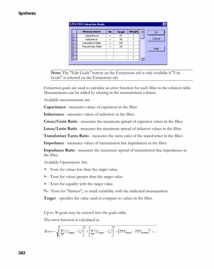
Synthesis
382
Note: The "Edit Goals" button on the Extractions tab is only available if "Use Goals" is selected on the Extractions tab.
Extraction goals are used to calculate an error function for each filter in the solution table. Measurements can be added by clicking in the measurement column.
Available measurements are:
Capacitance - measures values of capacitors in the filter.
Inductance - measures values of inductors in the filter.
Cmax/Cmin Ratio - measures the maximum spread of capacitor values in the filter.
Lmax/Lmin Ratio - measures the maximum spread of inductor values in the filter.
Transformer Turns Ratio - measures the turns ratio of the transformer in the filter.
Impedance - measures values of transmission line impedances in the filter.
Impedance Ratio - measures the maximum spread of transmission line impedances in the filter.
Available Opererators Are:
< - Tests for values less than the target value.
> - Tests for values greater than the target value.
= - Tests for equality with the target value.
% - Tests for "flatness", or small variability with the indicated measurement.
Target - specifies the value used to compare to values in the filter.
Up to 30 goals may be entered into the goals table.
The error function is calculated as

S/FILTER
383
Note: In the error function above, only the measurements entered into the Goals dialog table are actually evaluated. Also, only cases that produce error are calculated. For example, if the target is capacitance<10 pF, and all capacitors are less than 10 pF, no error function is calculated (error=0).
S/FILTER calculates the error function for each filter when "Use Goals" is selected on the Extractions tab.
The Customize Permutation Table Dialog The Customize Permutation Table dialog is shown below:
This dialog is used to customize what measurements are shown in the solutions table on the Extractions tab, and in what order.
Available - this box shows the available measurements that are not selected for showing in the solutions table on the Extractions tab.
Show In Table - this box shows the measurements that have been selected for showing in the solutions table on the Extractions tab.
- moves the measurement selected in "Show In Table" back to "Available".
- moves the measurement selected in "Available" to "Show In Table".
- moves all measurements from "Show In Table" to "Available".
- moves all measurements from "Available" to "Show In Table".
Measurements are shown with the abbreviated name in parentheses. The abbreviated name is used when displaying measurements in the solutions table on the Extractions tab.
Synthesis
384
Measurements available for use in the solutions table:
Minimum L Value - indicates the minimum value of inductance in the filter.
Maximum L Value - indicates the maximum value of inductance in the filter.
Minimum C Value - indicates the minimum value of capacitance in the filter.
Maximum C Value - indicates the maximum value of capacitance in the filter.
# Capacitors - total number of capacitors in the filter.
# Inductors - total number of inductance in the filter.
Permutation Extraction Order - shows the order of extraction for the zeros in the filter. Every filter has a unique extraction order.
# Resonators - the total number of LC tank resonators in the filter.
# Series Open Stubs - the number of series open stub transmission lines. These are wireline models and are unrealizable in most topologies.
# Series Res. in Series - the number of series resonators in series in the filter, as shown below:
# Series Res. to Ground - the number of series resonators to ground in the filter, as shown below:
# Series Shorted Stubs - the number of series open stub transmission lines. These are wireline models and are unrealizable in most topologies.
# Shunt Open Stubs - the number of standard open stub transmission lines.
# Shunt Res. to Ground - the number of parallel resonators to ground in the filter, as shown below:
# Shunt Res. in Series - the number of parallel resonators in series in the filter, as shown below:

S/FILTER
385
# Shunt Shorted Stubs - the number of shorted open stub transmission lines.
Cmax/Cmin Ratio - the ratio of maximum capacitance value to minimum capacitance value.
Equivalent Load Impedance - the value of load impedance that would be required if the transformer was removed from the filter.
Has Neg Parts? (Yes or No) - indicates whether any element in the filter has a negative value.
Lmax/Lmin Ratio - the ratio of maximum inductance value to minimum inductance value.
Maximum TLine Impedance - the maximum Zo of any line in the filter.
Maximum TLine Length - the maximum length in degrees of any line in the filter.
Minimum TLine Impedance - the minimum Zo of any line in the filter.
Minimum TLine Length - the minimum length in degrees of any line in the filter.
Permutation Error - the value of the error function calculated for the filter.
Transformer Turns Ratio - indicates the number of turns in the filter's transformer secondary. The number of turns in the primary is always 1.
The Shape Wizard Clicking the Shape Wizard button on the Specifications Tab in S/FILTER launches the Shape Wizard dialog. This dialog is shown below:
The Shape Wizard fills in the S/FILTER prompts to give the desired filter type and shape. For Butterworth and Chebyshev filters, this process is simply fills in prompts on the Specifications tab with data from the Shape Wizard dialog. For elliptic filters, however,

Synthesis
386
S/FILTER also calculates the location of finite transmission zeros for the desired filter and fills in the Zero Table.
Chebyshev and Elliptic filters use the passband definitions shown in the figure below:
The Shape Wizard options are:
Butterworth (Max Flat) - designs a filter with a flat passband, and no finite transmission zeros. Nth order Butterworth lowpass filters have N zeros at infinity, whereas Nth order Butterworth highpass filters have N zeros at DC. Nth order Butterworth bandpass filters have N zeros at both DC and infinity. Classic Butterworth filters have no finite transmission zeros, although they can be added manually in the Zero Table.
Chebyshev (Equiripple) - designs a filter with equal-amplitude passband ripple (equiripple), and no finite transmission zeros. Nth order Chebyshev lowpass filters have N zeros at infinity, whereas Nth order Chebyshev highpass filters have N zeros at DC. Nth order Chebyshev bandpass filters have N zeros at both DC and infinity. Classic Chebyshev filters have no finite transmission zeros, although they can be added manually in the Zero Table.
Elliptic (Equiripple) - designs a filter with equal-amplitude passband ripple (equiripple), and finite transmission zeros, which yield stopband ripple. The minimum order for Elliptic filters is 3. Odd order Elliptic filters have 1 transmission zero at infinity for lowpass, 1 transmission zero at DC for highpass, and 1 zero at both DC and infinity for bandpass filters. Odd order Elliptic filters have (N-1)/2 finite transmission zeros, whereas even order Elliptic filters have (N-2)/2 finite zeros. When this option is selected, Min. Stopband Attenuation (dB) specifies the minimum amount of stopband attenuation.
Elliptic filters use the stopband definitions given in the figure below:
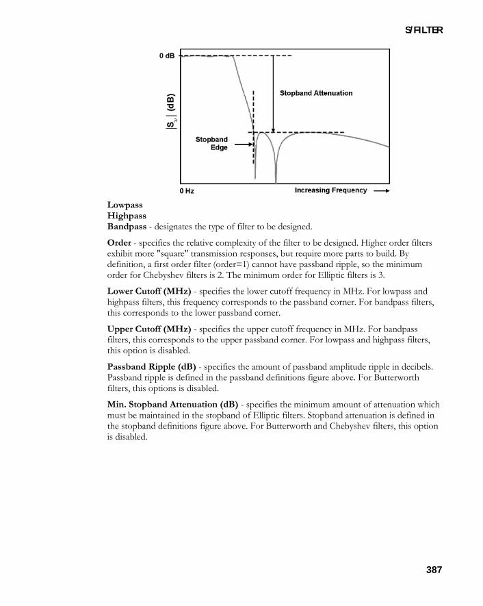
S/FILTER
387
Lowpass Highpass Bandpass - designates the type of filter to be designed.
Order - specifies the relative complexity of the filter to be designed. Higher order filters exhibit more "square" transmission responses, but require more parts to build. By definition, a first order filter (order=1) cannot have passband ripple, so the minimum order for Chebyshev filters is 2. The minimum order for Elliptic filters is 3.
Lower Cutoff (MHz) - specifies the lower cutoff frequency in MHz. For lowpass and highpass filters, this frequency corresponds to the passband corner. For bandpass filters, this corresponds to the lower passband corner.
Upper Cutoff (MHz) - specifies the upper cutoff frequency in MHz. For bandpass filters, this corresponds to the upper passband corner. For lowpass and highpass filters, this option is disabled.
Passband Ripple (dB) - specifies the amount of passband amplitude ripple in decibels. Passband ripple is defined in the passband definitions figure above. For Butterworth filters, this options is disabled.
Min. Stopband Attenuation (dB) - specifies the minimum amount of attenuation which must be maintained in the stopband of Elliptic filters. Stopband attenuation is defined in the stopband definitions figure above. For Butterworth and Chebyshev filters, this option is disabled.

389
Chapter 11: Signal Control
Signal Control: Operation
Signal Control Overview The Signal Control Synthesis module enables the user to design splitters, couplers, baluns, and attenuators. These elements may be implemented using either distributed (i.e. transmission lines) or lumped (e.g. resistors and capacitors) components. The following paragraphs describe the design process, types of signal control elements, and some of the basic terminology and concepts.
Design Process The design process begins with the definition of requirements. For a coupler, for example, these may consist of the coupling, input reflection, and directivity (i.e. isolation – coupling) over the frequency range of interest. These requirements can be entered directly by the user, or transferred automatically from the corresponding behavioral schematic element. The user can then select from a range of possible implementations. These are organized by the phase relationship between the output signals. For the couplers, the outputs can be in-phase, i.e. directional couplers, or 90 degrees out-of-phase (90-degree hybrid couplers). The implementations are further divided into classes and subclasses.
After an implementation is chosen, the synthesis module computes a schematic of an initial design. The goal of this design is to meet the requirements at the center frequency of the specified frequency band. A graph is created to display the commonly used performance parameters (e.g. S11, S21, S31, etc.). Optimization goals are automatically generated from the design requirements. The user now has the option of optimizing the design using these goals, or revising the goals. Another option is to tune the various parameters manually to determine the relative sensitivities. If the design is in terms of transmission lines, a particular manufacturing process can be selected. The schematic will be converted to that process (e.g. microstrip or stripline) will maintaining the frequency response at the design frequency. This design could be adjusted or re-optimized if necessary. A layout of the design can be automatically generated from the schematic. This can be used for electromagnetic simulations or board layout.
The design process can be summarized in terms of the following steps:
1. Define requirements.
2. Select implementation type based on output phase relationships.
3. Optimize design or adjust parameters based on performance trade-offs.
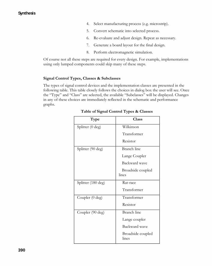
Synthesis
390
4. Select manufacturing process (e.g. microstrip).
5. Convert schematic into selected process.
6. Re-evaluate and adjust design. Repeat as necessary.
7. Generate a board layout for the final design.
8. Perform electromagnetic simulation.
Of course not all these steps are required for every design. For example, implementations using only lumped components could skip many of these steps.
Signal Control Types, Classes & Subclasses The types of signal control devices and the implementation classes are presented in the following table. This table closely follows the choices in dialog box the user will see. Once the “Type” and “Class” are selected, the available “Subclasses” will be displayed. Changes in any of these choices are immediately reflected in the schematic and performance graphs.
Table of Signal Control Types & Classes
Type Class
Splitter (0 deg) Wilkinson
Transformer
Resistor
Splitter (90 deg) Branch line
Lange Coupler
Backward wave
Broadside coupled lines
Splitter (180 deg) Rat-race
Transformer
Coupler (0 deg) Transformer
Resistor
Coupler (90 deg)
Branch line
Lange coupler
Backward wave
Broadside coupled lines

Signal Control
391
Balun Lange Coupler
Transformer
Lumped
Half Wave
Quarter Wave Coax
Attenuator Resistor
Dialog Box For User Selection of Types, Classes & Subclasses
Definitions The following definitions are used in this document:
Splitter: A device with equal signal levels at each output port.
Coupler: A device for extracting a fixed amount of the input signal.
Combiner: A splitter used with multiple inputs and a single output (i.e. inputs and outputs reversed)
Port Conventions For the purposes of this synthesis module the following port numbering and naming conventions were adopted.
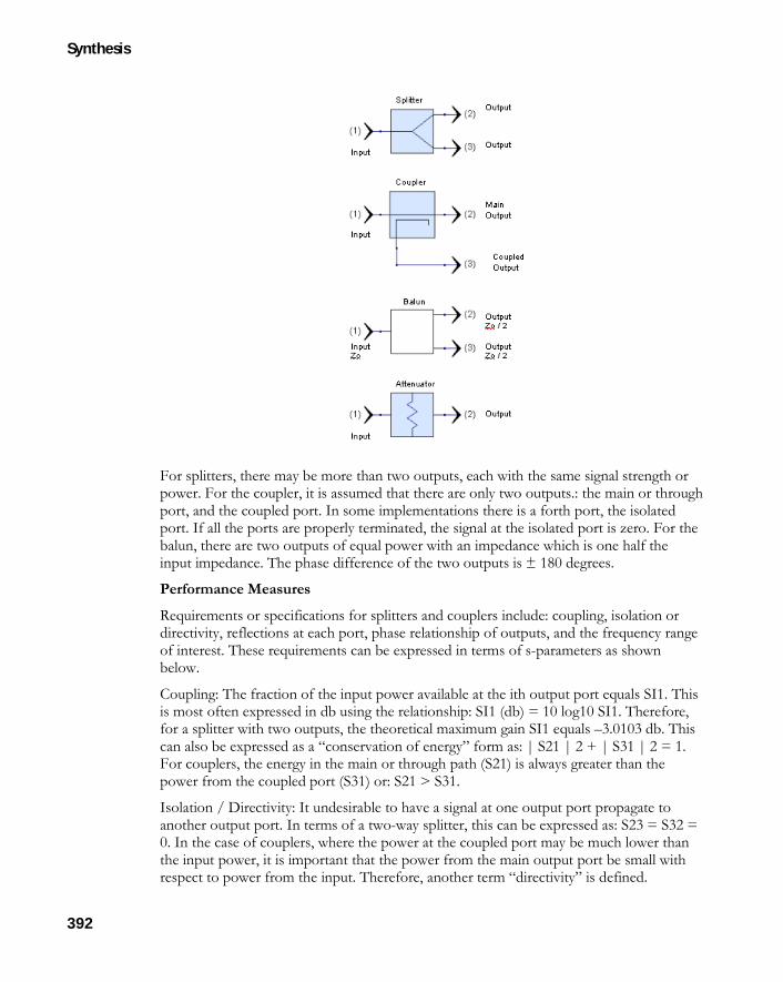
Synthesis
392
For splitters, there may be more than two outputs, each with the same signal strength or power. For the coupler, it is assumed that there are only two outputs.: the main or through port, and the coupled port. In some implementations there is a forth port, the isolated port. If all the ports are properly terminated, the signal at the isolated port is zero. For the balun, there are two outputs of equal power with an impedance which is one half the input impedance. The phase difference of the two outputs is ± 180 degrees.
Performance Measures Requirements or specifications for splitters and couplers include: coupling, isolation or directivity, reflections at each port, phase relationship of outputs, and the frequency range of interest. These requirements can be expressed in terms of s-parameters as shown below.
Coupling: The fraction of the input power available at the ith output port equals SI1. This is most often expressed in db using the relationship: SI1 (db) = 10 log10 SI1. Therefore, for a splitter with two outputs, the theoretical maximum gain SI1 equals –3.0103 db. This can also be expressed as a “conservation of energy” form as: | S21 | 2 + | S31 | 2 = 1. For couplers, the energy in the main or through path (S21) is always greater than the power from the coupled port (S31) or: S21 > S31.
Isolation / Directivity: It undesirable to have a signal at one output port propagate to another output port. In terms of a two-way splitter, this can be expressed as: S23 = S32 = 0. In the case of couplers, where the power at the coupled port may be much lower than the input power, it is important that the power from the main output port be small with respect to power from the input. Therefore, another term “directivity” is defined.
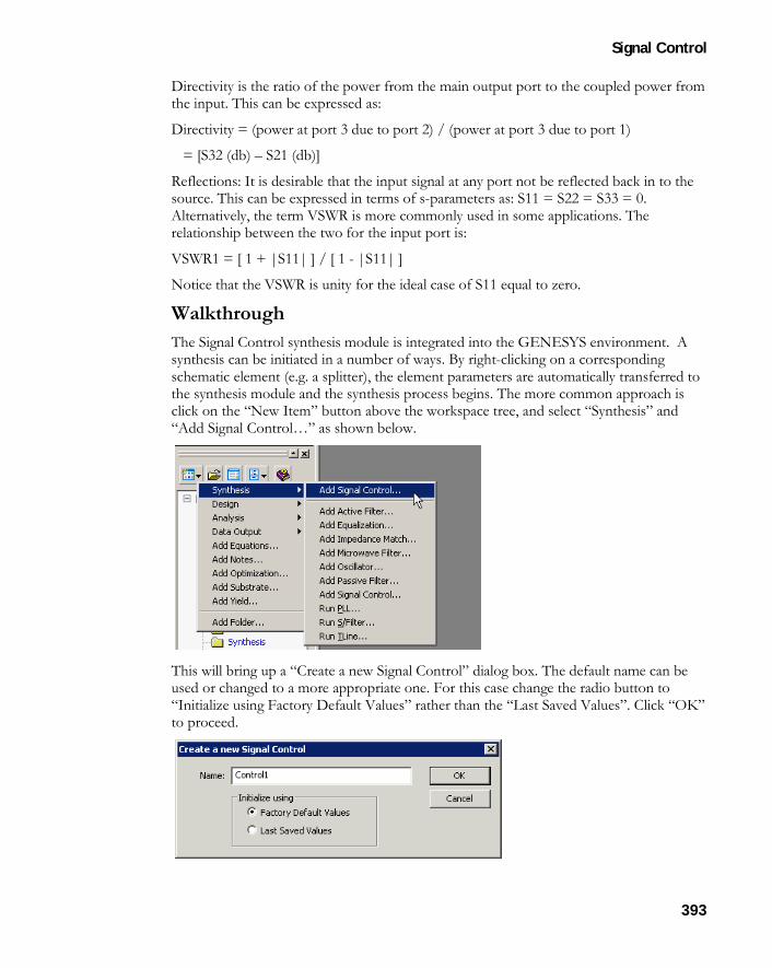
Signal Control
393
Directivity is the ratio of the power from the main output port to the coupled power from the input. This can be expressed as:
Directivity = (power at port 3 due to port 2) / (power at port 3 due to port 1)
= [S32 (db) – S21 (db)]
Reflections: It is desirable that the input signal at any port not be reflected back in to the source. This can be expressed in terms of s-parameters as: S11 = S22 = S33 = 0. Alternatively, the term VSWR is more commonly used in some applications. The relationship between the two for the input port is:
VSWR1 = [ 1 + |S11| ] / [ 1 - |S11| ]
Notice that the VSWR is unity for the ideal case of S11 equal to zero.
Walkthrough The Signal Control synthesis module is integrated into the GENESYS environment. A synthesis can be initiated in a number of ways. By right-clicking on a corresponding schematic element (e.g. a splitter), the element parameters are automatically transferred to the synthesis module and the synthesis process begins. The more common approach is click on the “New Item” button above the workspace tree, and select “Synthesis” and “Add Signal Control…” as shown below.
This will bring up a “Create a new Signal Control” dialog box. The default name can be used or changed to a more appropriate one. For this case change the radio button to “Initialize using Factory Default Values” rather than the “Last Saved Values”. Click “OK” to proceed.

Synthesis
394
A synthesis named “Control1” will be created with the factory default values. A “Signal Control Properties” dialog box will appear, along with a schematic and performance graph as seen below. The dialog box is used to control the design process. There are four pages or tabs: Topology, Settings, Options, and Summary. The Topology page shows that the nominal design is a Wilkinson Quarter Wave splitter. By clicking on the down arrow in the “Type” box, all of the available types are displayed. These are: Splitter (0 deg), Splitter (90 deg), Splitter (180 deg), Coupler (directional), Coupler (90 deg hybrid), Balun, and Attenuator. Similarly clicking the down arrow in the “Class” box displays the available classes for the selected type. Finally, for the selected type and class, a set of “radio buttons” appears for the subclasses, if any.
The defaults will be used for this example. Clicking on the “Settings” tab will reveal the input parameters which are appropriate of this configuration. If the synthesis had been invoked from a schematic element, these values would be filled in from that element. Shown are the factory default values for a Wilkinson splitter. The Reference Impedance is 50 ohms and the coupling is the theoretical value for a splitter with two outputs. Notice that “Number of Outputs” is one of the input parameters. To change the number of outputs, click in the box and up/down arrows appear. Click on an arrow and the number is incremented or decremented. Alternately, the number can be highlighted by holding down the mouse button and passing the cursor over the number. A new number can now be entered. Hit the return key to complete the data entry. Notice that changing the number of outputs also changes the coupling value. In this sense, the coupling value is not an input at all, but a display of the coupling which corresponds to the selected number of outputs.
The isolation and input reflection values are designated as “optimization goals”, and as such do not enter into the generation of the initial design. Their use will be described later. Similarly, the upper and lower cutoff frequencies are also part of the optimization process. However, they are used to compute the “center” or design frequency. The initial design is
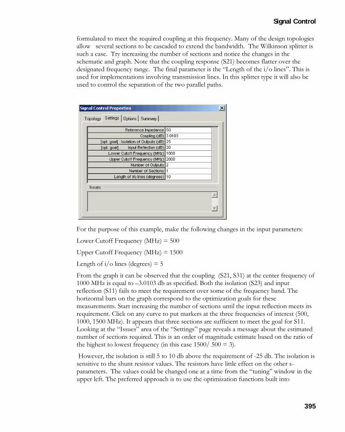
Signal Control
395
formulated to meet the required coupling at this frequency. Many of the design topologies allow several sections to be cascaded to extend the bandwidth. The Wilkinson splitter is such a case. Try increasing the number of sections and notice the changes in the schematic and graph. Note that the coupling response (S21) becomes flatter over the designated frequency range. The final parameter is the “Length of the i/o lines”. This is used for implementations involving transmission lines. In this splitter type it will also be used to control the separation of the two parallel paths.
For the purpose of this example, make the following changes in the input parameters:
Lower Cutoff Frequency (MHz) = 500
Upper Cutoff Frequency (MHz) = 1500
Length of i/o lines (degrees) = 5
From the graph it can be observed that the coupling (S21, S31) at the center frequency of 1000 MHz is equal to –3.0103 db as specified. Both the isolation (S23) and input reflection (S11) fails to meet the requirement over some of the frequency band. The horizontal bars on the graph correspond to the optimization goals for these measurements. Start increasing the number of sections until the input reflection meets its requirement. Click on any curve to put markers at the three frequencies of interest (500, 1000, 1500 MHz). It appears that three sections are sufficient to meet the goal for S11. Looking at the “Issues” area of the “Settings” page reveals a message about the estimated number of sections required. This is an order of magnitude estimate based on the ratio of the highest to lowest frequency (in this case 1500/ 500 = 3).
However, the isolation is still 5 to 10 db above the requirement of -25 db. The isolation is sensitive to the shunt resistor values. The resistors have little effect on the other s-parameters. The values could be changed one at a time from the “tuning” window in the upper left. The preferred approach is to use the optimization functions built into
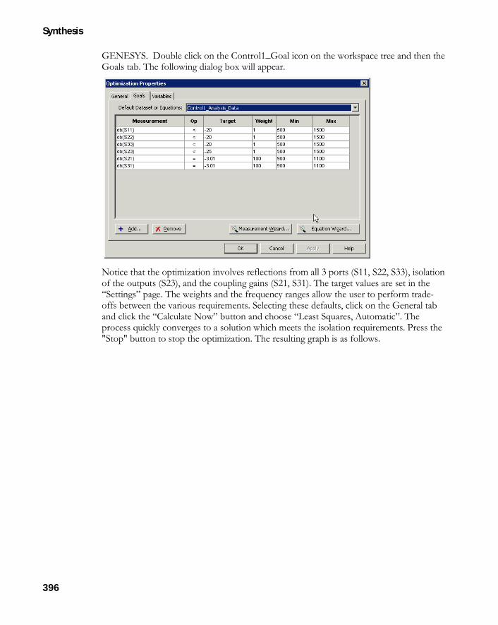
Synthesis
396
GENESYS. Double click on the Control1_Goal icon on the workspace tree and then the Goals tab. The following dialog box will appear.
Notice that the optimization involves reflections from all 3 ports (S11, S22, S33), isolation of the outputs (S23), and the coupling gains (S21, S31). The target values are set in the “Settings” page. The weights and the frequency ranges allow the user to perform trade-offs between the various requirements. Selecting these defaults, click on the General tab and click the “Calculate Now” button and choose “Least Squares, Automatic”. The process quickly converges to a solution which meets the isolation requirements. Press the "Stop" button to stop the optimization. The resulting graph is as follows.
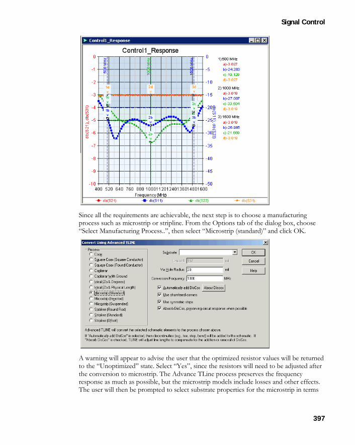
Signal Control
397
Since all the requirements are achievable, the next step is to choose a manufacturing process such as microstrip or stripline. From the Options tab of the dialog box, choose “Select Manufacturing Process..”, then select “Microstrip (standard)” and click OK.
A warning will appear to advise the user that the optimized resistor values will be returned to the “Unoptimized” state. Select “Yes”, since the resistors will need to be adjusted after the conversion to microstrip. The Advance TLine process preserves the frequency response as much as possible, but the microstrip models include losses and other effects. The user will then be prompted to select substrate properties for the microstrip in terms

Synthesis
398
of dielectric constants, thickness, and properties of the metal layer. For this exercise choose the default substrate.
The resulting schematic has the ideal transmission line elements replaced with microstrip models and has inserted “discos” or discontinuity models for the bends in the lines. As expected, the isolation response no longer meets the requirement and the coupling response has evidence of losses. The coupling response is still balanced, in that S21 = S31 across the frequency band. Assuming that the coupling response is acceptable, the resistor values will be re-optimized to restore acceptable isolation performance.
The optimized response again meets the requirements for isolation and reflections at all ports. The above process is not the only way to design the splitter. The widths and lengths
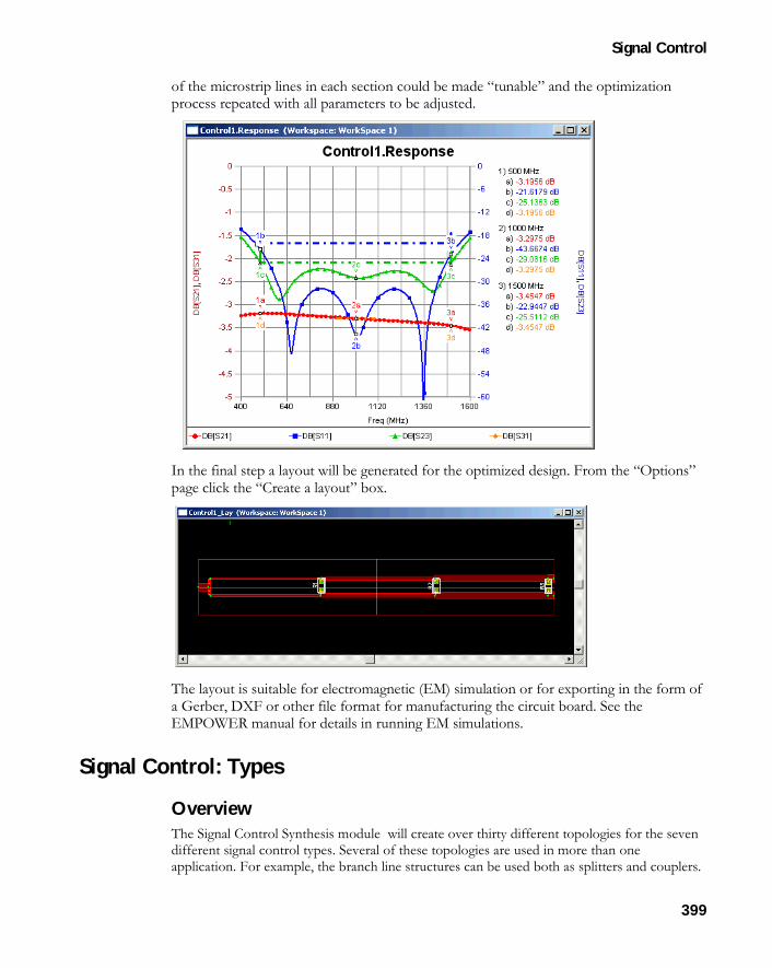
Signal Control
399
of the microstrip lines in each section could be made “tunable” and the optimization process repeated with all parameters to be adjusted.
In the final step a layout will be generated for the optimized design. From the “Options” page click the “Create a layout” box.
The layout is suitable for electromagnetic (EM) simulation or for exporting in the form of a Gerber, DXF or other file format for manufacturing the circuit board. See the EMPOWER manual for details in running EM simulations.
Signal Control: Types
Overview The Signal Control Synthesis module will create over thirty different topologies for the seven different signal control types. Several of these topologies are used in more than one application. For example, the branch line structures can be used both as splitters and couplers.

Synthesis
400
The “Signal Control Properties” dialog box organizes these topologies by type, class, and subclass. The following table shows where the topologies fit into this organization. The organization follows how a user might look up a part in a catalog. It also supports the option of right-clicking on a schematic element of a device such as a two-way splitter and automatically initiating the synthesis function with the given parameters.
Type Class Subclasses
Splitter (0 deg) Wilkinson Transformer Resistor
Quarter Wavelength, Loaded, Lumped
Splitter (90 deg) Branch line Lange coupler Backward wave Broadside coupled lines
Quarter Wavelength, Coupled Lines, Loaded, Lumped Tandem
Splitter (180 deg) Rat-Race Transformer
1.5 wavelength, Coupled Lines, Loaded, Lumped
Coupler (0 deg) Transformer Resistor
Coupler (90 deg) Branch line Lange coupler Backward wave Broadside coupled lines
Quarter Wavelength, Coupled Lines, Loaded, Lumped See note below
Balun Lange coupler Transformer Lumped Half Wave Quarter Wave Coax
Attenuator Resistor Pi Network, Tee Network
Backward wave coupler subclasses: Width Symmetric, Width Asymmetric, Velocity Compensated Lumped, Loaded, Tandem, Multi-section Symmetric, Multi-section Asymmetric.
Types
For the descriptions of the different types, the following organization is used:
1. Wilkinson splitters
2. Backward wave (splitters / couplers)
3. Branch line (splitters / couplers)
4. Lange couplers
5. Broadside coupled lines
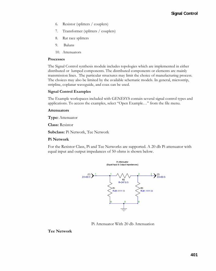
Signal Control
401
6. Resistor (splitters / couplers)
7. Transformer (splitters / couplers)
8. Rat race splitters
9. Baluns
10. Attenuators
Processes
The Signal Control synthesis module includes topologies which are implemented in either distributed or lumped components. The distributed components or elements are mainly transmission lines. The particular structures may limit the choice of manufacturing process. The choices may also be limited by the available schematic models. In general, microstrip, stripline, coplanar waveguide, and coax can be used.
Signal Control Examples
The Example workspaces included with GENESYS contain several signal control types and applications. To access the examples, select “Open Example…” from the file menu.
Attenuators Type: Attenuator
Class: Resistor
Subclass: Pi Network, Tee Network
Pi Network For the Resistor Class, Pi and Tee Networks are supported. A 20 db Pi attenuator with equal input and output impedances of 50 ohms is shown below.
Pi Attenuator With 20 db Attenuation
Tee Network
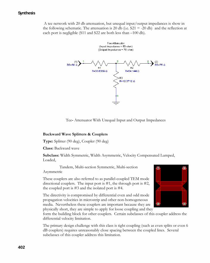
Synthesis
402
A tee network with 20 db attenuation, but unequal input/output impedances is show in the following schematic. The attenuation is 20 db (i.e. S21 = -20 db) and the reflection at each port is negligible (S11 and S22 are both less than –100 db).
Tee- Attenuator With Unequal Input and Output Impedances
Backward Wave Splitters & Couplers Type: Splitter (90 deg), Coupler (90 deg)
Class: Backward wave
Subclass: Width Symmetric, Width Asymmetric, Velocity Compensated Lumped, Loaded,
Tandem, Multi-section Symmetric, Multi-section Asymmetric
These couplers are also referred to as parallel-coupled TEM mode directional couplers. The input port is #1, the through port is #2, the coupled port is #3 and the isolated port is #4.
The directivity is compromised by differential even and odd mode propagation velocities in microstrip and other non-homogeneous media. Nevertheless these couplers are important because they are physically short, they are simple to apply for loose coupling and they form the building block for other couplers. Certain subclasses of this coupler address the differential velocity limitation.
The primary design challenge with this class is tight coupling (such as even splits or even 6 dB couplers) requires unreasonably close spacing between the coupled lines. Several subclasses of this coupler address this limitation.

Signal Control
403
Width Symmetric In the context of a single section coupler the term symmetric refers to the fact that both line widths are equal. With multiple section couplers, symmetry is also used to signify whether the coupling of each section is symmetric mirrored about the input and output (left and right). To avoid confusion we will use the specific terms width symmetric and coupling symmetric.
The basic formulae are:
k=10^(-CouplingDB/20) ex. k=0.316 for a 10 dB coupler
Zoe=Zo*SQR[(1+k)/(1-k)] ex. Zoe=69.37
Zoo=Zo*SQR[(1-k)/(1+k)] Zoo=36.04
Reference
G. Matthaei, L. Young, E. Jones, Microwave Filters, Impedance-Matching Networks and Coupling Structures, Artech House.
Width Asymmetric In the context of a single section coupler the term asymmetric refers to the fact that the line widths are unequal. This is necessary only where the impedance of the coupled port is different than the input and through port.
Velocity Compensated Lumped The directivity is compromised by differential even and odd mode propagation velocities in microstrip and other non-homogeneous media. One method to compensate for this is to place loading capacitors that bridge the ends of the coupled lines. This slows the velocity for the odd-mode only to equalize the velocities. (It electrically lengthens the lines for the odd mode).
Reference
D. Kajfez, Raise Coupler Directivity with Lumped Compensation, Microwaves & RF, March 1978, pp. 64-70.
Loaded The physical length of the coupler may be decreased by adding lumped capacitors to ground at the end of each coupled line. Too much loading causes narrow coupled line spacing. Combining loading and lumped compensation requires six lumped capacitors but results in wide spacing, broader bandwidth and flatter coupling responses.
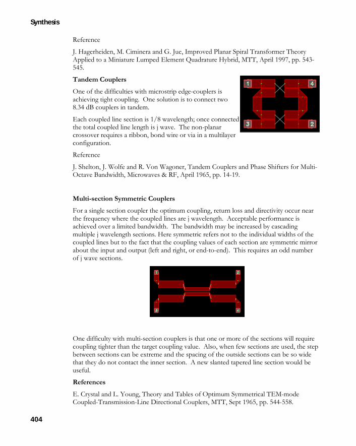
Synthesis
404
Reference
J. Hagerheiden, M. Ciminera and G. Jue, Improved Planar Spiral Transformer Theory Applied to a Miniature Lumped Element Quadrature Hybrid, MTT, April 1997, pp. 543-545.
Tandem Couplers One of the difficulties with microstrip edge-couplers is achieving tight coupling. One solution is to connect two 8.34 dB couplers in tandem.
Each coupled line section is 1/8 wavelength; once connected the total coupled line length is ј wave. The non-planar crossover requires a ribbon, bond wire or via in a multilayer configuration.
Reference
J. Shelton, J. Wolfe and R. Von Wagoner, Tandem Couplers and Phase Shifters for Multi-Octave Bandwidth, Microwaves & RF, April 1965, pp. 14-19.
Multi-section Symmetric Couplers For a single section coupler the optimum coupling, return loss and directivity occur near the frequency where the coupled lines are ј wavelength. Acceptable performance is achieved over a limited bandwidth. The bandwidth may be increased by cascading multiple ј wavelength sections. Here symmetric refers not to the individual widths of the coupled lines but to the fact that the coupling values of each section are symmetric mirror about the input and output (left and right, or end-to-end). This requires an odd number of ј wave sections.
One difficulty with multi-section couplers is that one or more of the sections will require coupling tighter than the target coupling value. Also, when few sections are used, the step between sections can be extreme and the spacing of the outside sections can be so wide that they do not contact the inner section. A new slanted tapered line section would be useful.
References E. Crystal and L. Young, Theory and Tables of Optimum Symmetrical TEM-mode Coupled-Transmission-Line Directional Couplers, MTT, Sept 1965, pp. 544-558.
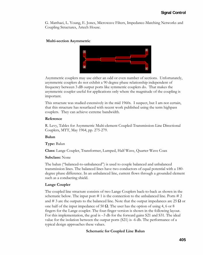
Signal Control
405
G. Matthaei, L. Young, E. Jones, Microwave Filters, Impedance-Matching Networks and Coupling Structures, Artech House.
Multi-section Asymmetric
Asymmetric couplers may use either an odd or even number of sections. Unfortunately, asymmetric couplers do not exhibit a 90 degree phase relationship independent of frequency between 3 dB output ports like symmetric couplers do. That makes the asymmetric coupler useful for applications only where the magnitude of the coupling is important.
This structure was studied extensively in the mid 1960s. I suspect, but I am not certain, that this structure has resurfaced with recent work published using the term highpass couplers. They can achieve extreme bandwidth.
Reference R. Levy, Tables for Asymmetric Multi-element Coupled-Transmission-Line Directional Couplers, MTT, May 1964, pp. 275-279.
Balun Type: Balun
Class: Lange Coupler, Transformer, Lumped, Half Wave, Quarter Wave Coax
Subclass: None
The balun (“balanced-to-unbalanced”) is used to couple balanced and unbalanced transmission lines. The balanced lines have two conductors of equal potential with a 180-degree phase difference. In an unbalanced line, current flows through a grounded element such as a conducting shield.
Lange Coupler The coupled line structure consists of two Lange Couplers back-to-back as shown in the schematic below. The input port # 1 is the connection to the unbalanced line. Ports # 2 and # 3 are the outputs to the balanced line. Note that the output impedances are 25 Ω or one half of the input impedance of 50 Ω. The user has the option of using 4, 6 or 8 fingers for the Lange coupler. The four-finger version is shown in the following layout. For this implementation, the goal is –3 db for the forward gains S21 and S31. The ideal value for the isolation between the output ports (S21) is -6 db. The performance of a typical design approaches these values.
Schematic for Coupled Line Balun

Synthesis
406
Layout for Coupled Line Balun
Transformer A more straightforward mechanization of the balun is the transformer balun. It is essentially a transformer with a single input winding for the unbalanced input and a center-tapped secondary for the balanced output. Generally, transformer baluns are used at lower frequencies (up to about 1 GHz).
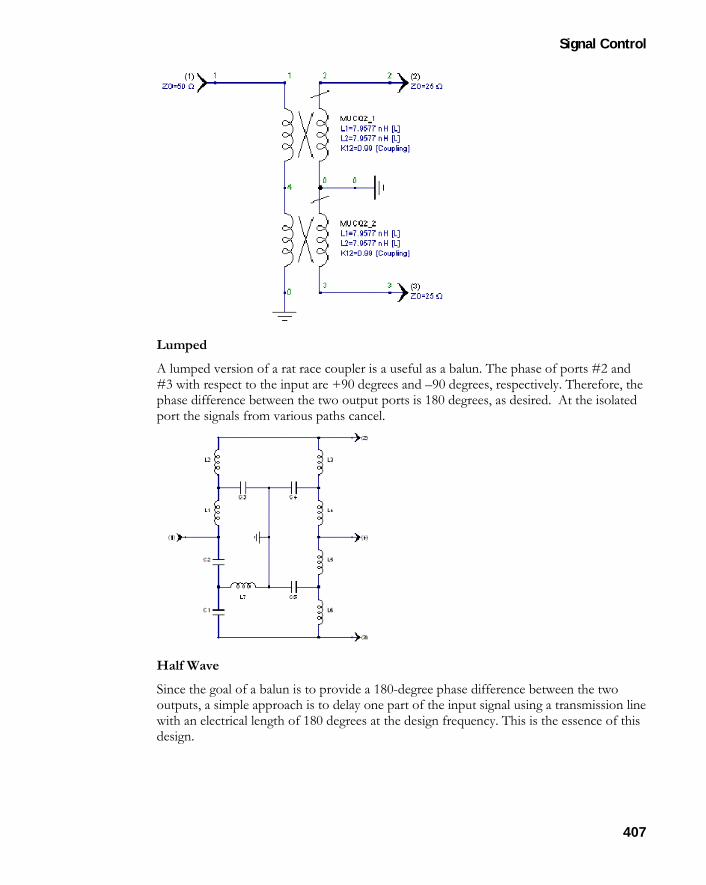
Signal Control
407
Lumped A lumped version of a rat race coupler is a useful as a balun. The phase of ports #2 and #3 with respect to the input are +90 degrees and –90 degrees, respectively. Therefore, the phase difference between the two output ports is 180 degrees, as desired. At the isolated port the signals from various paths cancel.
Half Wave Since the goal of a balun is to provide a 180-degree phase difference between the two outputs, a simple approach is to delay one part of the input signal using a transmission line with an electrical length of 180 degrees at the design frequency. This is the essence of this design.
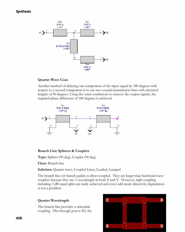
Synthesis
408
Quarter Wave Coax Another method of delaying one component of the input signal by 180 degrees with respect to a second component is to use two coaxial transmission lines with electrical lengths of 90 degrees. Using the outer conductors to remove the output signals, the required phase difference of 180 degrees is achieved.
Branch Line Splitters & Couplers Type: Splitter (90 deg), Coupler (90 deg)
Class: Branch line
Subclass: Quarter wave, Coupled Lines, Loaded, Lumped
The branch line (or branch-guide) is direct coupled. They are larger than backward wave couplers because they are ¼ wavelength in both X and Y. However, tight coupling including 3 dB equal splits are easily achieved and even/odd mode directivity degradation is not a problem.
Quarter Wavelength The branch line provides a selectable coupling. The through port is #2, the
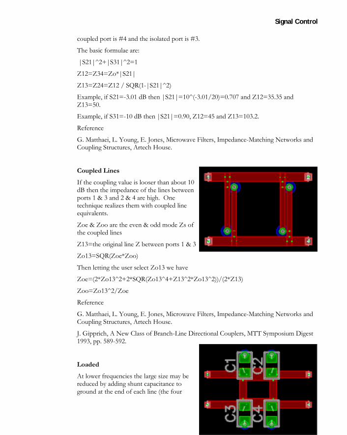
Signal Control
409
coupled port is #4 and the isolated port is #3.
The basic formulae are:
|S21|^2+|S31|^2=1
Z12=Z34=Zo*|S21|
Z13=Z24=Z12 / SQR(1-|S21|^2)
Example, if S21=-3.01 dB then |S21|=10^(-3.01/20)=0.707 and Z12=35.35 and Z13=50.
Example, if S31=-10 dB then |S21|=0.90, Z12=45 and Z13=103.2.
Reference
G. Matthaei, L. Young, E. Jones, Microwave Filters, Impedance-Matching Networks and Coupling Structures, Artech House.
Coupled Lines If the coupling value is looser than about 10 dB then the impedance of the lines between ports 1 & 3 and 2 & 4 are high. One technique realizes them with coupled line equivalents.
Zoe & Zoo are the even & odd mode Zs of the coupled lines
Z13=the original line Z between ports 1 & 3
Zo13=SQR(Zoe*Zoo)
Then letting the user select Zo13 we have
Zoe=(2*Zo13^2+2*SQR(Zo13^4+Z13^2*Zo13^2))/(2*Z13)
Zoo=Zo13^2/Zoe
Reference
G. Matthaei, L. Young, E. Jones, Microwave Filters, Impedance-Matching Networks and Coupling Structures, Artech House.
J. Gipprich, A New Class of Branch-Line Directional Couplers, MTT Symposium Digest 1993, pp. 589-592.
Loaded At lower frequencies the large size may be reduced by adding shunt capacitance to ground at the end of each line (the four

Synthesis
410
corners). This reduces the line lengths. It also reduces the coupler line widths which may be beneficial for reducing the effect of corner discontinuities. It may be a disadvantage with large coupling values where the lines between ports 1&3 are 2&4 are already too narrow. It is possible the load only the thru lines with the same four capacitors.
References
T. Hirota, A. Minakawa and M. Muraguchi, Reduced-Size Branch-Line and Rat-Race Hybrids for Uniplanar MMICs, MTT, Mar 1990, pp. 270-275.
Lumped Taken to the extreme, the loaded branch-line coupler becomes a lumped circuit. They are suitable for low-frequency and ultra-miniature high-frequency branch-line couplers.
Reference
M. Caulton, e. al., Status of Lumped Elements in Microwave Integrated Circuit – Present and Future, MTT, Jul 1991, pp. 558-599.
Broadside Coupled Lines Type: Splitter (90 deg), Coupler (90 deg)
Class: Broadside Coupled Lines
Subclass: None
A tightly coupled pair of transmission lines can be achieved by broadside coupling. This is suitable for use as a splitter and has a very symmetrical response about the center frequency. As with the backward wave approach, the line length is quarter wavelength. This topology is typically used with stripline. The coupling is primarily a function of the spacing (s) between the lines.
Cross-sectional View Of Broadside Coupled Stripline
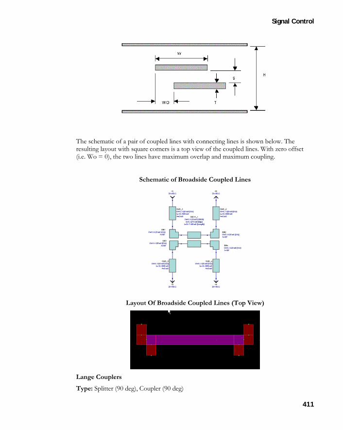
Signal Control
411
The schematic of a pair of coupled lines with connecting lines is shown below. The resulting layout with square corners is a top view of the coupled lines. With zero offset (i.e. Wo = 0), the two lines have maximum overlap and maximum coupling.
Schematic of Broadside Coupled Lines
Layout Of Broadside Coupled Lines (Top View)
Lange Couplers Type: Splitter (90 deg), Coupler (90 deg)
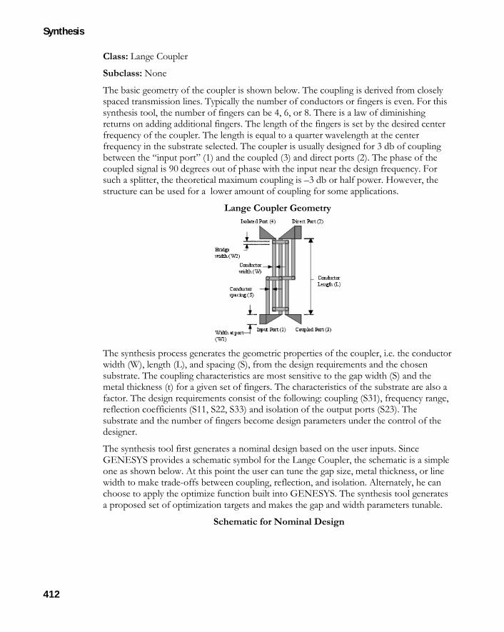
Synthesis
412
Class: Lange Coupler
Subclass: None
The basic geometry of the coupler is shown below. The coupling is derived from closely spaced transmission lines. Typically the number of conductors or fingers is even. For this synthesis tool, the number of fingers can be 4, 6, or 8. There is a law of diminishing returns on adding additional fingers. The length of the fingers is set by the desired center frequency of the coupler. The length is equal to a quarter wavelength at the center frequency in the substrate selected. The coupler is usually designed for 3 db of coupling between the “input port” (1) and the coupled (3) and direct ports (2). The phase of the coupled signal is 90 degrees out of phase with the input near the design frequency. For such a splitter, the theoretical maximum coupling is –3 db or half power. However, the structure can be used for a lower amount of coupling for some applications.
Lange Coupler Geometry
The synthesis process generates the geometric properties of the coupler, i.e. the conductor width (W), length (L), and spacing (S), from the design requirements and the chosen substrate. The coupling characteristics are most sensitive to the gap width (S) and the metal thickness (t) for a given set of fingers. The characteristics of the substrate are also a factor. The design requirements consist of the following: coupling (S31), frequency range, reflection coefficients (S11, S22, S33) and isolation of the output ports (S23). The substrate and the number of fingers become design parameters under the control of the designer.
The synthesis tool first generates a nominal design based on the user inputs. Since GENESYS provides a schematic symbol for the Lange Coupler, the schematic is a simple one as shown below. At this point the user can tune the gap size, metal thickness, or line width to make trade-offs between coupling, reflection, and isolation. Alternately, he can choose to apply the optimize function built into GENESYS. The synthesis tool generates a proposed set of optimization targets and makes the gap and width parameters tunable.
Schematic for Nominal Design
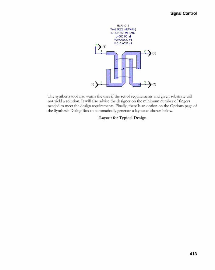
Signal Control
413
The synthesis tool also warns the user if the set of requirements and given substrate will not yield a solution. It will also advise the designer on the minimum number of fingers needed to meet the design requirements. Finally, there is an option on the Options page of the Synthesis Dialog Box to automatically generate a layout as shown below.
Layout for Typical Design
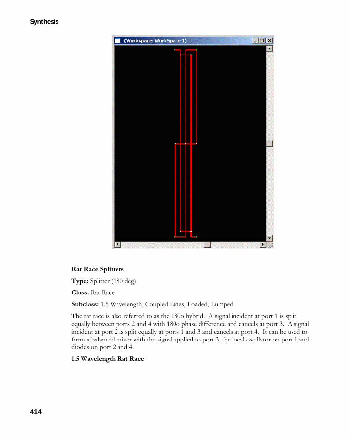
Synthesis
414
Rat Race Splitters Type: Splitter (180 deg)
Class: Rat Race
Subclass: 1.5 Wavelength, Coupled Lines, Loaded, Lumped
The rat race is also referred to as the 180o hybrid. A signal incident at port 1 is split equally between ports 2 and 4 with 180o phase difference and cancels at port 3. A signal incident at port 2 is split equally at ports 1 and 3 and cancels at port 4. It can be used to form a balanced mixer with the signal applied to port 3, the local oscillator on port 1 and diodes on port 2 and 4.
1.5 Wavelength Rat Race

Signal Control
415
The rat race can be realized with straight-lines. However, customers are accustomed to the round shape and inflexible customers would protest. The need for the lines to interface connectors on the walls of a rectangular housing and coupler asymmetry will require use of equations to define the geometry. A disadvantage of the rat-race coupler is the relatively large size.
Coupled-Line Rat-Race The ¾ wavelength section can be replaced with a ¼ wavelength long coupled line. This significantly decreases the size, facilitates a rectangular shape and increases the useful bandwidth.
Unfortunately, the even-mode impedance of the coupled lines is 5.83X higher than the odd-mode impedance. This large ratio results in extremely close line spacing which is nearly impossible in edge-coupled microstrip on soft-board substrates. Broadside coupling and MMIC process may be more feasible.
Loaded Rat-Race The ¾ wavelength section is replaced with a lumped pi highpass (shunt L, series C and shunt L) and the ¼ wavelength sections are replaced with 1/8-wavelength lines loaded with capacitors to ground at each end. The resulting structure is shown at the right. This structure is very compact.
Lumped-Element Rat-Race
Synthesis
416
The ¾ wavelength section is replaced with a highpass tee and the ¼ wavelength long sections are replaced with lowpass networks.
Reference
S.J. Parisi, A Lumped Element Rat-Race Coupler, Applied Microwave & Wireless, Aug/Sept 1989, pp. 84-93.
Resistor Splitters & Couplers Type: Splitter (0 deg), Couplers (0 deg)
Class: Resistor
Subclass: None
Splitter: The resistive splitter may be the simplest of splitters, but it has some serious drawbacks compared to distributed or more complex lumped networks. The equation for the resistors is:
R = [(N – 1) / (N+1)] Zo where N = number of outputs, Zo = reference impedance
This equation forces the input impedance to be Zo, so there is no reflection at this port. However, the splitter has high losses. The gain at each output port is –6 db, compared to –3 db for a Wilkinson splitter. In addition, the isolation is relatively poor. The isolation is equal to the coupling. For a two-way splitter, the isolation and coupling are 6 db.
Coupler: The resistive coupler does have the same issues with losses and isolation as the resistive splitter. The directivity, which is equal to the isolation minus the coupling, is therefore zero db. However, the addition of another resistor allows the network to be matched at all three ports.
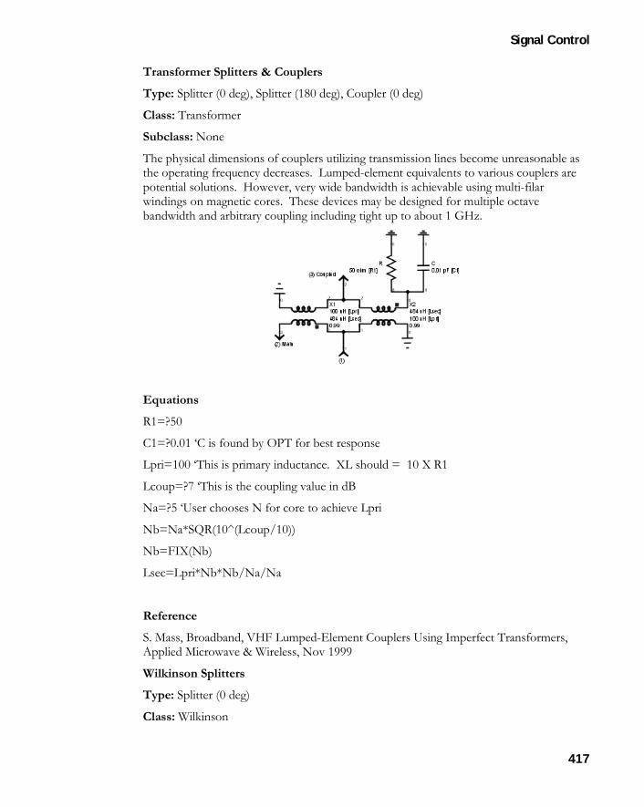
Signal Control
417
Transformer Splitters & Couplers Type: Splitter (0 deg), Splitter (180 deg), Coupler (0 deg)
Class: Transformer
Subclass: None
The physical dimensions of couplers utilizing transmission lines become unreasonable as the operating frequency decreases. Lumped-element equivalents to various couplers are potential solutions. However, very wide bandwidth is achievable using multi-filar windings on magnetic cores. These devices may be designed for multiple octave bandwidth and arbitrary coupling including tight up to about 1 GHz.
Equations
R1=?50
C1=?0.01 ‘C is found by OPT for best response
Lpri=100 ‘This is primary inductance. XL should = 10 X R1
Lcoup=?7 ‘This is the coupling value in dB
Na=?5 ‘User chooses N for core to achieve Lpri
Nb=Na*SQR(10^(Lcoup/10))
Nb=FIX(Nb)
Lsec=Lpri*Nb*Nb/Na/Na
Reference S. Mass, Broadband, VHF Lumped-Element Couplers Using Imperfect Transformers, Applied Microwave & Wireless, Nov 1999
Wilkinson Splitters Type: Splitter (0 deg)
Class: Wilkinson
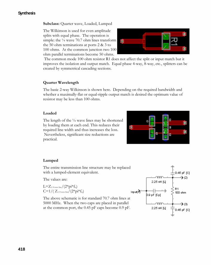
Synthesis
418
Subclass: Quarter wave, Loaded, Lumped
The Wilkinson is used for even amplitude splits with equal phase. The operation is simple: the ¼ wave 70.7 ohm lines transform the 50 ohm terminations at ports 2 & 3 to 100 ohms. At the common junction two 100 ohm parallel terminations become 50 ohms. The common mode 100 ohm resistor R1 does not affect the split or input match but it improves the isolation and output match. Equal phase 4-way, 8-way, etc., splitters can be created by symmetrical cascading sections.
Quarter Wavelength The basic 2-way Wilkinson is shown here. Depending on the required bandwidth and whether a maximally-flat or equal-ripple output match is desired the optimum value of resistor may be less than 100 ohms.
Loaded The length of the ¼ wave lines may be shortened by loading them at each end. This reduces their required line width and thus increases the loss. Nevertheless, significant size reductions are practical.
Lumped The entire transmission line structure may be replaced with a lumped-element equivalent.
The values are:
L=Z1/4 wave line/(2*pi*fo) C=1/( Z1/4 wave line/(2*pi*fo)
The above schematic is for standard 70.7 ohm lines at 5000 MHz. When the two caps are placed in parallel at the common port, the 0.45 pF caps become 0.9 pF.
419
Chapter 12: TLINE
Overview TLINE analyzes and synthesizes an extensive variety of transmission line structures. New for Version 8, TLINE will automatically convert an electrical schematic to physical transmission lines. The routines use the most recent and accurate models available, and include the effects of metalization thickness, surface roughness and dispersion. The expressions for microstrip are the most sophisticated. Over 24 types of transmission line structures are supported. In addition to analyzing and synthesizing line impedance, other important line performance parameters are computed.
TLINE is used to convert between electrical transmission lines (characterized by impedance and length in degrees) and physical transmission lines (such as microstrip, characterized by physical dimensions). TLINE can be run in two modes: Standalone and Advanced.
In standalone mode, you enter physical dimensions, and TLINE will tell you the physical characteristics. TLINE can also synthesize line dimensions from specified electrical characteristics. If you are familiar to other programs or utilities for transmission line calculations, they operate in this type of standalone mode.
In the advanced mode, your circuits are automatically converted from electrical to physical descriptions. This includes the addition of discontinuities as necessary (in the form of DisCo's). This revolutionary feature is available exclusively from Eagleware.
Standalone Operation
Starting TLINE The standalone mode of TLINE is started from the Synthesis folder on the workspace tree. Right-click on the Synthesis folder and Select "Run TLine...". Alternately, press the "New Item" button on the workspace window, select "Synthesis", then "Run TLine...". This process is shown below, where TLine is at the bottom of the list.
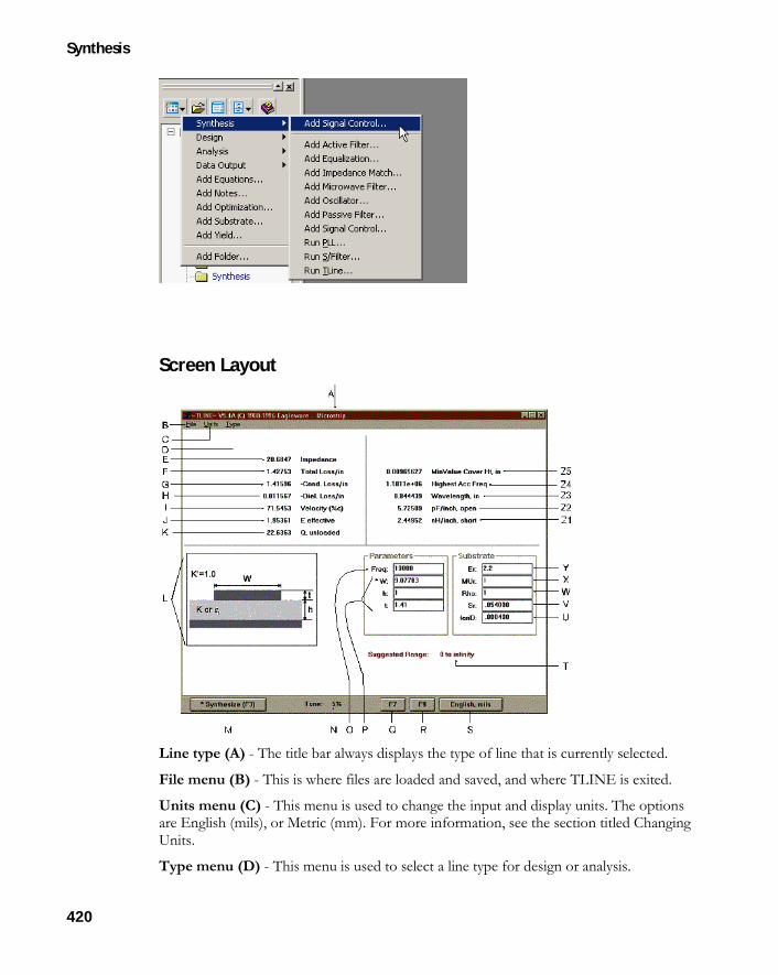
Synthesis
420
Screen Layout
Line type (A) - The title bar always displays the type of line that is currently selected.
File menu (B) - This is where files are loaded and saved, and where TLINE is exited.
Units menu (C) - This menu is used to change the input and display units. The options are English (mils), or Metric (mm). For more information, see the section titled Changing Units.
Type menu (D) - This menu is used to select a line type for design or analysis.
TLINE
421
Line impedance (E) - This value is the current line impedance calculated from the user-specified data.
Total line loss (F) - This value is given in decibels per unit length (inch or meter) for the current line. It is simply the sum of the conductor loss and dielectric loss (G and H in the figure). For more information, see the section titled Output Parameters.
Conductor loss (G) - This value is given in decibels per unit length (inch or meter) for the current line. For more information, see the section titled Output Parameters.
Dielectric loss (H) - This value is given in decibels per unit length (inch or meter) for the current line. For more information, see the section titled Output Parameters.
Propagation velocity (I) - This value is given as a percentage of the free space speed of light (). For more information, see the section titled Output Parameters.
e effective (J) - This is the effective dielectric constant for the current line. For homogeneous lines, this value is equal to the relative dielectric constant (see prompt Y below). For more information, see the section titled Output Parameters.
Unloaded Q (K) - This is the maximum quality factor of the current line with no external loading. For more information, see the section titled Output Parameters.
Picture (L) - shows line cross section and variable definitions. This picture changes to reflect the current line type. The picture shown in this example is of a microstrip line.
Synthesize button (M) - This button launches the synthesizer for calculation of line dimensions for a given impedance. The F3 on this button means that the synthesizer can also be started by pressing F3.
Current tune percentage (N) - Prompt values are always tuned according to this value. For more information, see the section titled Changing Input Parameters.
Frequency prompt (O) - This is the operating frequency in MHz. This example specifies 10000 MHz (10 GHz).
Dimension prompts (P) - These prompts define the line dimensions. The variable definitions are given in the picture on the left (see L above).
Note: An asterisk (*) next to a prompt means that the corresponding dimension can be automatically calculated by clicking the synthesize button (see “M” above).
Tune down button (Q) - This button decreases the tune percentage (see H above). For more information, see the section titled Changing Input Parameters.
Tune up button (R) - This button increases the tune percentage (see H above). For more information, see the section titled Changing Input Parameters.
Units button (S) - This button toggles the current units between “mils” and “mm”. The current units are shown on the button. The Units menu (see C above) can also be used to toggle the units. All line dimensions are assumed to be in the current units. For more information, see the section titled Changing Units.

Synthesis
422
Suggested range (T) - The value shown is the suggested range for the prompt that the cursor is currently in. If a value is entered outside its suggested range, the calculated data may not be accurate.
Loss tangent (U) - This prompt specifies the dielectric loss tangent for the indicated area on the picture (usually shown as k). Pressing F1 while in this box shows typical loss tangent values.
Surface roughness (V) - This prompt indicates the maximum metal surface variations (roughness) in the current units. Pressing F1 while in this prompt shows typical values.
Resistivity (W) - This prompt indicates the metal resistivity relative to copper. A value of 1 designates the metal as copper, and pressing F1 while in this box shows typical values for various configurations.
Relative permeability (X) - This prompt specifies the permeability of the dielectric relative to free space. Pressing F1 while in this prompt shows typical values. NOTE: Some lines require MUr=1, so this prompt may not be changeable for all types.
Relative permittivity (Y) - This prompt specifies the dielectric permittivity relative to free space. Pressing F1 while in this prompt displays typical values.
Line inductance (Z1) - This value is given in nano-Henries, and specifies the short-circuit line inductance per unit length (inches or meters).
Line capacitance (Z2) - This value is given in pico-Farads, and specifies the open-circuit line capacitance per unit length (inches or meters).
Wavelength (Z3) - This value is the physical length of one wavelength at the frequency specified in prompt “O” above.
Highest accurate frequency (Z4) - This prompt specifies the highest frequency at which the current data should be considered accurate.
Minimum cover height (Z5) - This prompt specifies the minimum cover distance from the line for reasonable output parameter accuracy.
Operation The bottom part of the TLINE main window contains fields for data input. The top part contains resulting data for the transmission line(s) described by user input. At any time, press F1 for help on the input at the cursor location, or press Alt-F1 (hold down the Alt key and press F1) for general help.
The cursor is initially located in the “Freq” prompt. To continue to the next input field, press the Tab or Enter key. To go to the previous input field, press Shift-Tab. Optionally, the left mouse button may be used to move the cursor. When the cursor is on an input field you may type in a new value for that field. Entering new input data automatically updates the resulting output.
TLINE
423
Example Here’s an example of how to synthesize a 50 ohm microstrip transmission line of 1 ounce copper on 1 mm thick RT/Duroid 5880 at 12400 MHz.
Using the mouse or the cursor keys, select the “Type” menu. Next, select the “Rectangluar” option. Next, select “Microstrip” from the menu. The screen will change to contain the input fields for microstrip. The picture also changes to show the variables used in the microstrip line.
Since this example uses millimeters, the units button (labeled “S” in the screen layout section) should be labeled “Metric, mm”. If it is not, click the button to change the selected units.
Move the cursor (using the Tab key) to the numeric fields. Type in the following values (Note that the line width value is simply a guess of 1 mm):
Freq: 12400 W: 1 h: 1 t: 0.036 Er: 2.2 Rho: 1 Sr: 1 tanD: 9e-4
As these values are entered, the resulting analysis quickly appears on the top of the screen. The line width guess is too narrow and therefore the impedance is too high. The screen should now look like:
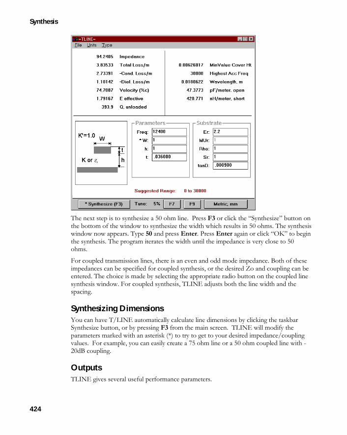
Synthesis
424
The next step is to synthesize a 50 ohm line. Press F3 or click the “Synthesize” button on the bottom of the window to synthesize the width which results in 50 ohms. The synthesis window now appears. Type 50 and press Enter. Press Enter again or click “OK” to begin the synthesis. The program iterates the width until the impedance is very close to 50 ohms.
For coupled transmission lines, there is an even and odd mode impedance. Both of these impedances can be specified for coupled synthesis, or the desired Zo and coupling can be entered. The choice is made by selecting the appropriate radio button on the coupled line synthesis window. For coupled synthesis, TLINE adjusts both the line width and the spacing.
Synthesizing Dimensions You can have T/LINE automatically calculate line dimensions by clicking the taskbar Synthesize button, or by pressing F3 from the main screen. TLINE will modify the parameters marked with an asterisk (*) to try to get to your desired impedance/coupling values. For example, you can easily create a 75 ohm line or a 50 ohm coupled line with -20dB coupling.
Outputs TLINE gives several useful performance parameters.
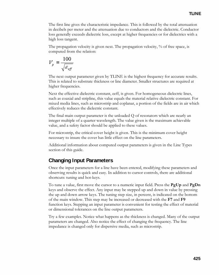
TLINE
425
The first line gives the characteristic impedance. This is followed by the total attenuation in decibels per meter and the attenuation due to conductors and the dielectric. Conductor loss generally exceeds dielectric loss, except at higher frequencies or for dielectrics with a high loss tangent.
The propagation velocity is given next. The propagation velocity, % of free space, is computed from the relation:
The next output parameter given by TLINE is the highest frequency for accurate results. This is related to substrate thickness or line diameter. Smaller structures are required at higher frequencies.
Next the effective dielectric constant, eeff, is given. For homogeneous dielectric lines, such as coaxial and stripline, this value equals the material relative dielectric constant. For mixed media lines, such as microstrip and coplanar, a portion of the fields are in air which effectively reduces the dielectric constant.
The final main output parameter is the unloaded Q of resonators which are nearly an integer multiple of a quarter wavelength. The value given is the maximum achievable value, and a safety factor should be applied to these values.
For microstrip, the critical cover height is given. This is the minimum cover height necessary to insure the cover has little effect on the line parameters.
Additional information about computed output parameters is given in the Line Types section of this guide.
Changing Input Parameters Once the input parameters for a line have been entered, modifying these parameters and observing results is quick and easy. In addition to cursor controls, there are additional shortcuts: tuning and hot-keys.
To tune a value, first move the cursor to a numeric input field. Press the PgUp and PgDn keys and observe the effect. Any input may be stepped up and down in value by pressing the up and down arrow keys. The tuning step size, in percent, is indicated on the bottom of the main window. This step may be increased or decreased with the F7 and F9 function keys. Stepping an input parameter is convenient for testing the effect of material or dimensional tolerances on the line output parameters.
Try a few examples. Notice what happens as the thickness is changed. Many of the output parameters are changed. Also notice the effect of changing the frequency. The line impedance is changed only for dispersive media, such as microstrip.
Synthesis
426
Units To change from English (mils) to metric (mm) units and vice versa, either select the units button (labeled either “English” or “Metric”) with the left mouse button or press Alt-U to select the Units menu and then select the desired units.
Automatic Defaults TLINE contains a convenient feature: Each time TLINE is exited, all the line parameters and dimensions are written to the DEFAULT.TL$ file. When TLINE is started again, those values are read and become the new default values. This means that the last screen used is restored every time TLINE is started.
Input Parameter Ranges During parameter inputs, guidelines are given for parameter ranges which yield accurate results. Parameters outside these ranges will be accepted to allow for situations where extreme values are required, and some degradation of accuracy must be accepted. The recommended ranges are selected so the equations used will be accurate for any combination of input parameters.
Some combinations of input parameters may cause a math error. In this case, all outputs will be displayed as “Error”. This ensures that TLINE does not report erroneous data when a math exception occurs.
If an error does occur, simply change the offending input parameter and TLINE will resume normal operation.
Advanced TLINE Operation
Overview Advanced TLINE is a time saving tool that allows the user to convert an existing electrical or physical transmission line topologies into 1 of 13 other electrical and physical transmission line topologies. The conversion takes into account changes in substrates, chamfered corners, symmetric steps, and transmission line discontinuities.
For more information, see the following topic: Advanced TLINE Dialog Box and Advanced TLINE Example.
Advanced TLINE Example In this example an electrical model of a Hairpin filter will be created. Advanced TLINE will be use to convert the electrical schematic to a Microstrip physical schematic and a Stripline physical schematic from which layouts can be created for both of these topologies. A second substrate will be added and a new Hairpin filter will be created from this substrate.

TLINE
427
Note: This example assumes that you are familiar with drawing schematics and entering parameters.
The figure below shows the original electrical schematic and the Advanced TLINE converted physical schematic from which the layout was derived.
Original Electrical Schematic
Converted Physical Schematic
Completed Hairpin Layout
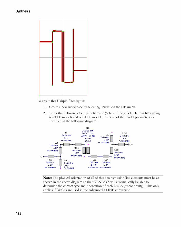
Synthesis
428
To create this Hairpin filter layout:
1. Create a new workspace by selecting “New” on the File menu.
2. Enter the following electrical schematic (Sch1) of the 2 Pole Hairpin filter using ten TLE models and one CPL model. Enter all of the model parameters as specified in the following diagram.
Note: The physical orientation of all of these transmission line elements must be as shown in the above diagram so that GENESYS will automatically be able to determine the correct type and orientation of each DisCo (discontinuity). This only applies if DisCos are used in the Advanced TLINE conversion.
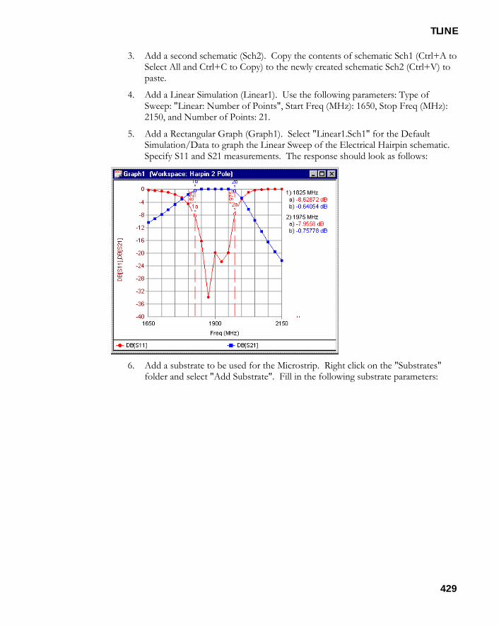
TLINE
429
3. Add a second schematic (Sch2). Copy the contents of schematic Sch1 (Ctrl+A to Select All and Ctrl+C to Copy) to the newly created schematic Sch2 (Ctrl+V) to paste.
4. Add a Linear Simulation (Linear1). Use the following parameters: Type of Sweep: "Linear: Number of Points", Start Freq (MHz): 1650, Stop Freq (MHz): 2150, and Number of Points: 21.
5. Add a Rectangular Graph (Graph1). Select "Linear1.Sch1" for the Default Simulation/Data to graph the Linear Sweep of the Electrical Hairpin schematic. Specify S11 and S21 measurements. The response should look as follows:
6. Add a substrate to be used for the Microstrip. Right click on the "Substrates"
folder and select "Add Substrate". Fill in the following substrate parameters:

Synthesis
430
7. Select the Hairpin electrical schematic (Sch2).
Note: Advanced TLINE will convert the entire selected (or active) schematic or ONLY the selected components in the selected schematic. If no elements have been selected in the active schematic then the entire schematic will be converted.
8. Select "Convert Using Advanced TLINE..." on the schematic menu. The Advanced TLINE dialog box will be opened.
9. Select the dialog information as follows:
then click OK.
10. If a substrate HAS NOT been defined the following dialog appears:

TLINE
431
and the user is given the opportunity to define a substrate before the conversion is completed. After this dialog is closed the Edit Substrate dialog box will appear.
11. Once Advanced TLINE has finished its conversion the the electrical schematic will be replaced with a physical schematic that looks like:
Notice that DisCos (discontinuities - round elements) have been placed onto the schematic at the appropriate discontinuity points (Automatically add DisCos checkbox) and that the physical lengths of the adjoining transmission lines have been adjusted to account for each discontinuity (Absorb DisCos, preserving circuit response when possible checkbox). For additional information on DisCos see Using Distributed Elements in the Users Guide.
Note: The orientation of the DisCos is based on the physical orientation of the transmission line elements in the original electrical schematic file. DisCo elements can be added manually by right clicking on the appropriate node and selecting the corresponding menu item.
12. Add a Rectangular Graph (Graph2). Select "Linear1.Sch2" for the Default Simulation/Data to graph the Linear Sweep of the Physical Hairpin schematic. Specify S11 and S21 measurements. The response should look as follows:
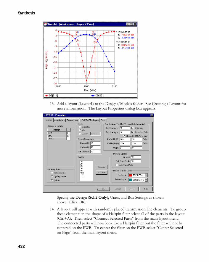
Synthesis
432
13. Add a layout (Layout1) to the Designs/Models folder. See Creating a Layout for
more information. The Layout Properties dialog box appears:
Specify the Design (Sch2 Only), Units, and Box Settings as shown above. Click OK.
14. A layout will appear with randomly placed transmission line elements. To group these elements in the shape of a Hairpin filter select all of the parts in the layout (Ctrl+A). Then select "Connect Selected Parts" from the main layout menu. The connected parts will now look like a Hairpin filter but the filter will not be centered on the PWB. To center the filter on the PWB select "Center Selected on Page" from the main layout menu.

TLINE
433
15. The Hairpin filter should now look like:
15. An EM simulation can be created, EM ports can be placed on the layout, the grid
can be adjusted, and an EMpower run can be made.
16. Advanced TLINE makes the job of changing the substrates real easy. To do this create a new substrate and load the "Rogers RO4003 1oz ED 32 mil" from the GENESYS Library. Click OK.
17. Select the previously converted Hairpin schematic (Sch2).
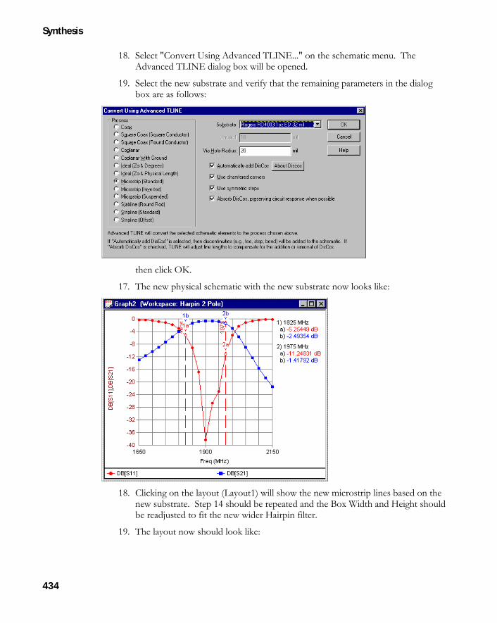
Synthesis
434
18. Select "Convert Using Advanced TLINE..." on the schematic menu. The Advanced TLINE dialog box will be opened.
19. Select the new substrate and verify that the remaining parameters in the dialog box are as follows:
then click OK.
17. The new physical schematic with the new substrate now looks like:
18. Clicking on the layout (Layout1) will show the new microstrip lines based on the
new substrate. Step 14 should be repeated and the Box Width and Height should be readjusted to fit the new wider Hairpin filter.
19. The layout now should look like:
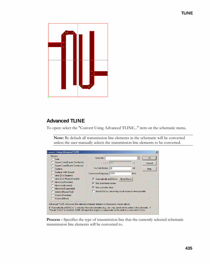
TLINE
435
Advanced TLINE To open: select the "Convert Using Advanced TLINE..." item on the schematic menu.
Note: By default all transmission line elements in the schematic will be converted unless the user manually selects the transmission line elements to be converted.
Process - Specifies the type of transmission line that the currently selected schematic transmission line elements will be converted to.
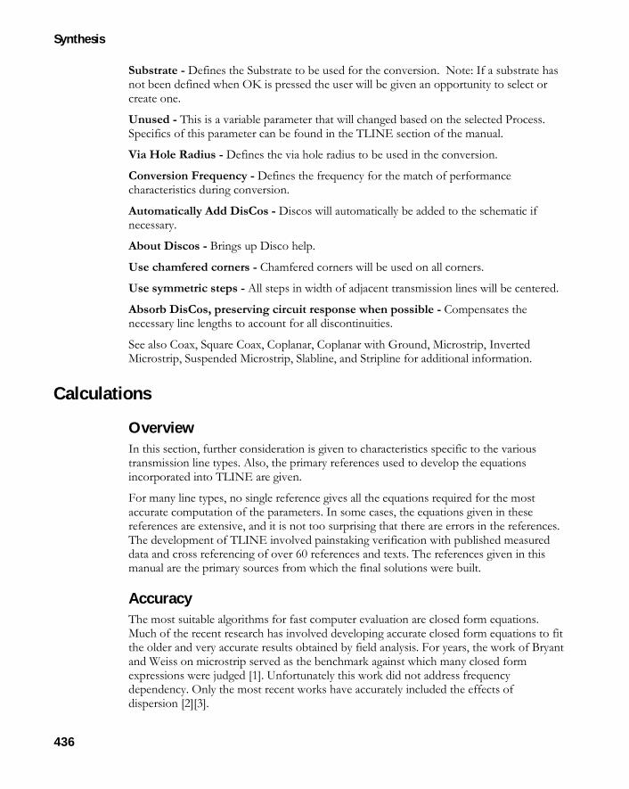
Synthesis
436
Substrate - Defines the Substrate to be used for the conversion. Note: If a substrate has not been defined when OK is pressed the user will be given an opportunity to select or create one.
Unused - This is a variable parameter that will changed based on the selected Process. Specifics of this parameter can be found in the TLINE section of the manual.
Via Hole Radius - Defines the via hole radius to be used in the conversion.
Conversion Frequency - Defines the frequency for the match of performance characteristics during conversion.
Automatically Add DisCos - Discos will automatically be added to the schematic if necessary.
About Discos - Brings up Disco help.
Use chamfered corners - Chamfered corners will be used on all corners.
Use symmetric steps - All steps in width of adjacent transmission lines will be centered.
Absorb DisCos, preserving circuit response when possible - Compensates the necessary line lengths to account for all discontinuities.
See also Coax, Square Coax, Coplanar, Coplanar with Ground, Microstrip, Inverted Microstrip, Suspended Microstrip, Slabline, and Stripline for additional information.
Calculations
Overview In this section, further consideration is given to characteristics specific to the various transmission line types. Also, the primary references used to develop the equations incorporated into TLINE are given.
For many line types, no single reference gives all the equations required for the most accurate computation of the parameters. In some cases, the equations given in these references are extensive, and it is not too surprising that there are errors in the references. The development of TLINE involved painstaking verification with published measured data and cross referencing of over 60 references and texts. The references given in this manual are the primary sources from which the final solutions were built.
Accuracy The most suitable algorithms for fast computer evaluation are closed form equations. Much of the recent research has involved developing accurate closed form equations to fit the older and very accurate results obtained by field analysis. For years, the work of Bryant and Weiss on microstrip served as the benchmark against which many closed form expressions were judged [1]. Unfortunately this work did not address frequency dependency. Only the most recent works have accurately included the effects of dispersion [2][3].
TLINE
437
Results for impedance and effective dielectric constant over a wide range of input parameters are now sufficiently accurate to strain efforts of verification by measured data. TLINE results are generally within 1% over a wide range of input parameters. References in the program and in this manual to “accurate” results means about 1%.
Results for loss and unloaded Q are more difficult to verify by measured data. Consequently, the theory is less well tested, and the accuracy of these parameters is somewhat lower. Fortunately, loss usually has a secondary effect on circuit performance, and TLINE loss parameters are sufficiently accurate for general use.
Input Parameters The units used for input parameters in TLINE are either mils (1/1000 inch) or millimeters for dimensions, megahertz for frequency and unitless (relative) values for material properties.
The default values for input parameters are given below:
Conductor diameter: d=100 Ground spacing, or conductor diameter: b=200 Conductor spacing or substrate thickness: H=100 Conductor spacing: s=200 Coplanar waveguide ground spacing: g=10 Strip thickness: t=1.4 Strip width: w=50 Frequency: F=1000 Relative dielectric constant: Er=1 Relative permeability: MUr=1 Resistivity relative to copper: Rho=1 Metalization surface roughness, RMS: Sr=.001 Dielectric loss tangent: tanD=0 Secondary dielectric: k’=1 Susp. or inv. microstrip substrate thickness: a=31 Single line impedance target: Zo=50 Even mode impedance target: Zoe=55.28 Odd mode impedance target: Zoo=45.23 Coupled line impedance target: Zo=50 Coupling target: dB=20
When a transmission line is analyzed, the last entered values automatically become the new default value
Output Parameters In the classic analysis of coaxial and two-wire lines, the line impedance was defined as the square root of L/C . L and C were characteristics of the line, and thus the term characteristic impedance. The analysis of mixed media microstrip with a hybrid mode of propagation at high frequencies raises a question as to the true definition of impedance for

Synthesis
438
this line. Nevertheless, we make calculations and compare the results to measured data, and success justifies our liberties.
For coupled lines, the even, Zoe, and odd mode, Zoo, impedances are given. As the line spacing increases, the even and odd mode impedances converge to the single strip characteristic impedance. The characteristic impedance (the square root of Zoe x Zoo) is also given for coupled lines.
Effective Dielectric Constant The effective dielectric constant is equal to the relative dielectric constant for homogeneous media lines such as coaxial and stripline. The static (low frequency) effective dielectric constant of mixed media lines like microstrip and coplanar is lower than the relative dielectric constant because a portion of the fields are in air above the substrate. This static effective dielectric constant is a function of the relative dielectric constant of the substrate, the strip width and even the strip thickness. For microstrip, as the frequency is increased, more and more of the field is confined to the substrate, and the effective dielectric constant increases. The effective dielectric constant given by TLINE includes all of these effects.
For coupled lines, the effective dielectric constants for both even and odd modes are given. They are different, even for the static (low frequency) case, and the effect of dispersion is different for each mode.
Loss TLINE gives the total loss and the losses due to conductors and the dielectric. Units are decibels per unit length (inch or meter). In coupled lines, both conductors are assumed to have the same resistivity. Conductor loss predominates except for extremely lossy dielectrics and higher microwave frequencies.
Of primary consideration for the conductor loss is the skin depth. The resistance is computed based on this and corrections for surface roughness [4]. At higher frequencies, typical metalization roughness will increase the conductor loss. The surface roughness default value of 0.001 millimeters, RMS, is between typical electro-deposited (rougher) and rolled metal (smoother) values [5]. The conductor losses for the strip type lines are then computed considering the current distribution on the strip. Conductor losses are approximately proportional to the square root of the frequency.
Dielectric losses depend on the loss tangent of the substrate material, the relative and effective dielectric constants and the frequency. Dielectric loss is proportional to the frequency.
Other factors effecting loss are repeated flexure of lines, temperature, corrosion of conductors, contamination of the dielectric by jacket plasticizers, moisture contamination and periodic dimensional errors of long lines caused by manufacturing processes. The last effect can be very significant for long lines, causing deep and narrow bandwidth suck-outs. These factors aren’t modeled by TLINE because they exist in degrees depending on conditions.
TLINE
439
For coupled lines, both the even and odd mode losses are given. The odd mode losses exceed even mode losses, significantly so for small strip spacings.
Propagation Velocity The propagation velocity, as a percentage of the free space value, is computed from the relation:
The physical length of line, Length, for a desired electrical length in degrees, ldeg, is given by:
where K is a function of the desired Length units. Representative values are:
Kinches = 11803 Kfeet = 983.57 Kmillimeters = 299793 Kmeters = 299.793
The time delay in nanoseconds, Td, for a given physical length of line is:
Highest Frequency The next output parameter given by TLINE is the highest frequency for accurate results. For coaxial and stripline, this value represents the approximate TE01 cutoff frequency. For microstrip, this is the highest frequency for which the equations, including dispersion effects, are accurate [2][3]. Thinner substrates allow accurate results to higher frequencies. For microstrip, 1 millimeter substrates give accurate results to 30 GHz [3].
Cover The effects of a cover for microstrip aren’t modeled by TLINE. We had originally intended to include cover effects, but a study of the available literature and measured data indicated that available routines weren’t sufficiently accurate over a general range of input parameters to warrant use in a program with otherwise accurate equations.
Instead, a critical height of the cover above the strip is computed and given as an output parameter. If the cover height exceeds this critical value, it will effect line parameters less than 1%. The critical height is based on the work of Bedair [6]. Higher dielectric constants and narrower strips allow closer covers.
Synthesis
440
Resonator Q The next output parameter is the unloaded Q of resonators. The value given is the maximum achievable value, and it would be wise to apply a safety factor to these values. Radiation losses are not included in the loss or Q computations. When microstrip lines are used for transmission, radiation losses are generally insignificant. However, when microstrip lines are used as resonators, particularly low impedance lines on low dielectric constant substrates, radiation losses may be significant. For further information, refer to Vendelin, reference [7].
Coupling For coupled lines, the coupling in decibels for quarter- wave lines is given. This may be used for designing loosely-coupled couplers. For tight coupling, the required spacing between strips becomes very small, and direct coupled designs like Wilkinson or branch line, or more sophisticated coupled structures like Lange, should be used.
For 50 ohm coupled stripline with 0.018 mm metalization thickness and a minimum spacing of 0.1 mm, the approximate maximum couplings for substrate dielectric constants of 1, 2.2 and 10 are -13 dB, -10 dB and -5 dB respectively.
For 50 ohm coupled microstrip with 0.018 mm metalization thickness, the approximate maximum couplings for substrate dielectric constants of 1, 2.2 and 10 are -10 dB, -7 dB and -3 dB respectively. These limits are set by TLINE math overflow.
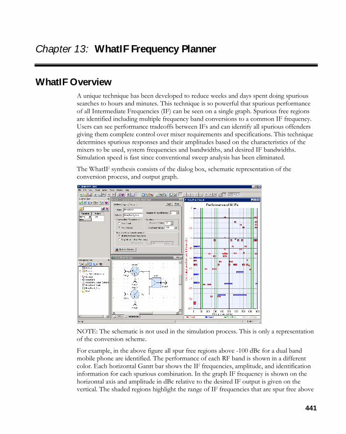
441
Chapter 13: WhatIF Frequency Planner
WhatIF Overview A unique technique has been developed to reduce weeks and days spent doing spurious searches to hours and minutes. This technique is so powerful that spurious performance of all Intermediate Frequencies (IF) can be seen on a single graph. Spurious free regions are identified including multiple frequency band conversions to a common IF frequency. Users can see performance tradeoffs between IFs and can identify all spurious offenders giving them complete control over mixer requirements and specifications. This technique determines spurious responses and their amplitudes based on the characteristics of the mixers to be used, system frequencies and bandwidths, and desired IF bandwidths. Simulation speed is fast since conventional sweep analysis has been eliminated.
The WhatIF synthesis consists of the dialog box, schematic representation of the conversion process, and output graph.
NOTE: The schematic is not used in the simulation process. This is only a representation of the conversion scheme.
For example, in the above figure all spur free regions above -100 dBc for a dual band mobile phone are identified. The performance of each RF band is shown in a different color. Each horizontal Gantt bar shows the IF frequencies, amplitude, and identification information for each spurious combination. In the graph IF frequency is shown on the horizontal axis and amplitude in dBc relative to the desired IF output is given on the vertical. The shaded regions highlight the range of IF frequencies that are spur free above
Synthesis
442
-100 dBc for a given spurious order. This entire simulation takes less than a fraction of second to run on an average PC, so the time saving in the development process is dramatic.
WhatIF Background Frequency planning is one the first steps performed during the RF architecture design phase. During this phase several frequency schemes are considered to ensure performance reliability internally as well as externally. External performance is typically controlled by a regulatory agency (i.e. Federal Communications Commission FCC or European Telecommunications Standards Institute ETSI) and the designer must comply with requirements before products are shipped and revenue collected. Spurious integrity for RF design is an age-old problem. Spurious responses, which occur naturally in the frequency conversion process, can render a particular design completely useless and non-compliant.
Spur Analysis Basics The frequency conversion equation is:
FIF = m x FRF ± n x FLO or FRF = m x FIF ± n x FLO
m = 0, 1, 2, …
n = 0, 1, 2, …
FIF = IF frequency
FRF = any frequency in the RF band
FLO = any frequency in the LO band
From this equation all spurious products can be determined. It’s easy to analyze frequencies that fall in a given IF band. Determining the amplitude of these spurious products is more challenging. But, selecting the best IF frequency can be difficult at best because of the time needed to create and analyze the hosts of data sets representing all of the possible spurious combinations for a single IF frequency. The process is further complicated for multiple band operation where a common IF is desired for all bands. Also, locating an input IF frequency while trying to maintain spectral purity across a wide output band is troublesome.
Traditional Approaches Traditional tools include spreadsheets, spur charts, and many other types of custom tools.
The following weaknesses of these tools are readily apparent:
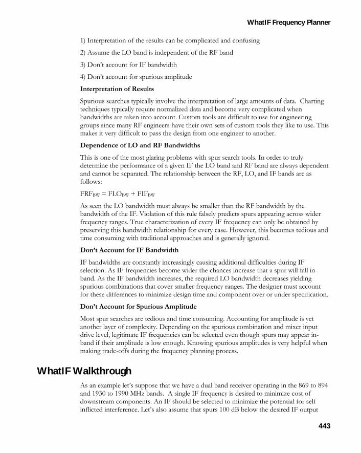
WhatIF Frequency Planner
443
1) Interpretation of the results can be complicated and confusing
2) Assume the LO band is independent of the RF band
3) Don’t account for IF bandwidth
4) Don’t account for spurious amplitude
Interpretation of Results Spurious searches typically involve the interpretation of large amounts of data. Charting techniques typically require normalized data and become very complicated when bandwidths are taken into account. Custom tools are difficult to use for engineering groups since many RF engineers have their own sets of custom tools they like to use. This makes it very difficult to pass the design from one engineer to another.
Dependence of LO and RF Bandwidths This is one of the most glaring problems with spur search tools. In order to truly determine the performance of a given IF the LO band and RF band are always dependent and cannot be separated. The relationship between the RF, LO, and IF bands are as follows:
FRFBW = FLOBW + FIFBW
As seen the LO bandwidth must always be smaller than the RF bandwidth by the bandwidth of the IF. Violation of this rule falsely predicts spurs appearing across wider frequency ranges. True characterization of every IF frequency can only be obtained by preserving this bandwidth relationship for every case. However, this becomes tedious and time consuming with traditional approaches and is generally ignored.
Don’t Account for IF Bandwidth IF bandwidths are constantly increasingly causing additional difficulties during IF selection. As IF frequencies become wider the chances increase that a spur will fall in-band. As the IF bandwidth increases, the required LO bandwidth decreases yielding spurious combinations that cover smaller frequency ranges. The designer must account for these differences to minimize design time and component over or under specification.
Don’t Account for Spurious Amplitude Most spur searches are tedious and time consuming. Accounting for amplitude is yet another layer of complexity. Depending on the spurious combination and mixer input drive level, legitimate IF frequencies can be selected even though spurs may appear in-band if their amplitude is low enough. Knowing spurious amplitudes is very helpful when making trade-offs during the frequency planning process.
WhatIF Walkthrough As an example let’s suppose that we have a dual band receiver operating in the 869 to 894 and 1930 to 1990 MHz bands. A single IF frequency is desired to minimize cost of downstream components. An IF should be selected to minimize the potential for self inflicted interference. Let’s also assume that spurs 100 dB below the desired IF output

Synthesis
444
level is our definition of spurious free. Other important design criteria are IF bandwidth of 1.25 MHz and maximum RF input mixer drive level of -10 dBm with a mixer LO level of +7 dBm for the 800 MHz mixer and 0 dBm input drive level with a mixer LO level of +10 dBm for the 1900 MHz mixer. It will also be assumed that a double balance mixer will be used to predict spurious amplitudes. Default values for the double balanced mixer is assumed.
DESIGN STEPS 1. Create a new frequency planner synthesis by clicking the ‘New’ button. Find the ‘Synthesis’ submenu and then select the ‘Add Frequency Planner’ submenu item.
2. Change the number of parallel mixers to 2.
3. Click the ‘Inputs’ tab to specify the parameters for the parameters for our conversion scheme.
4. Click ‘Mixer1’.
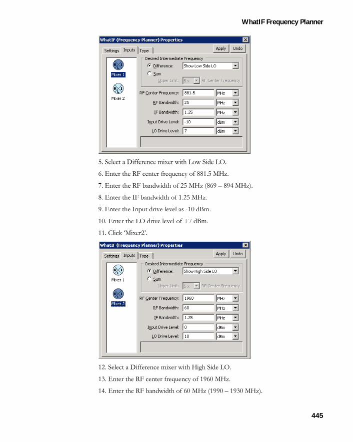
WhatIF Frequency Planner
445
5. Select a Difference mixer with Low Side LO.
6. Enter the RF center frequency of 881.5 MHz.
7. Enter the RF bandwidth of 25 MHz (869 – 894 MHz).
8. Enter the IF bandwidth of 1.25 MHz.
9. Enter the Input drive level as -10 dBm.
10. Enter the LO drive level of +7 dBm.
11. Click ‘Mixer2’.
12. Select a Difference mixer with High Side LO.
13. Enter the RF center frequency of 1960 MHz.
14. Enter the RF bandwidth of 60 MHz (1990 – 1930 MHz).

Synthesis
446
15. Enter the IF bandwidth of 1.25 MHz.
16. Enter the Input drive level of 0 dBm.
17. Enter the LO drive level of +10 dBm.
18. Click the ‘Apply’ button since defaults for all remaining parameters will be used.
The figure shows results in an easy to interpret format. The performance of every valid IF frequency that meets the requirements for both RF bands appears on a single graph. Mouse fly-over text is used to identify each spur and spur free region. For the first time in the industry, IF frequency selection is optimized since performance tradeoffs are quickly made despite complications from multiband operation. Notice in Figure 1 that the half-IF spur (2x2 from 0 to 119.375 MHz) is easily identified on the left of the graph and well as all spurious free regions shaded in green.
To demonstrate the analysis capability of WhatIF a spur free IF frequency of 772.85 MHz will be selected and analyzed. This spur free region can be identified on the right in preceding figure. On the ‘Settings’ tab of the ‘Frequency Planner Properties’ dialog box this frequency will be specified as the IF center frequency. When this IF frequency is specified an appropriate LO is created internally for both RF bands. This LO along with the specified RF bands will be analyzed using the appropriate equation (i.e. FIF = m x FRF ± n x FLO ). The mixer output is then displayed as shown in following figure. This display is equivalent to looking at the single IF spectrum output of the dual band conversion scheme on a spectrum analyzer. If the RF and LO frequencies where varied across their ranges we could track the 0 x -8 and 2 x 8 spur ranges. These ranges have also been plotted in the figure. Furthermore, these same spurs can be identified in preceding figure as the spurs bounding the selected spur-free region. As predicted in the performance in preceding figure the 772.85 MHz IF is indeed spur free to -100 dBc! Notice that the valid IF region is also shown for convenience.
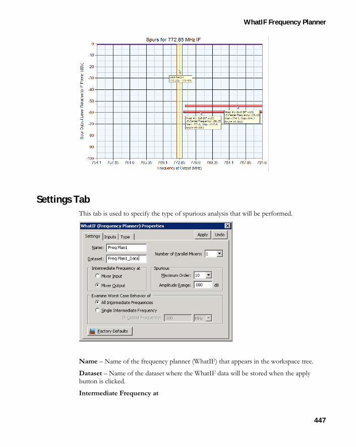
WhatIF Frequency Planner
447
Settings Tab This tab is used to specify the type of spurious analysis that will be performed.
Name – Name of the frequency planner (WhatIF) that appears in the workspace tree.
Dataset – Name of the dataset where the WhatIF data will be stored when the apply button is clicked.
Intermediate Frequency at
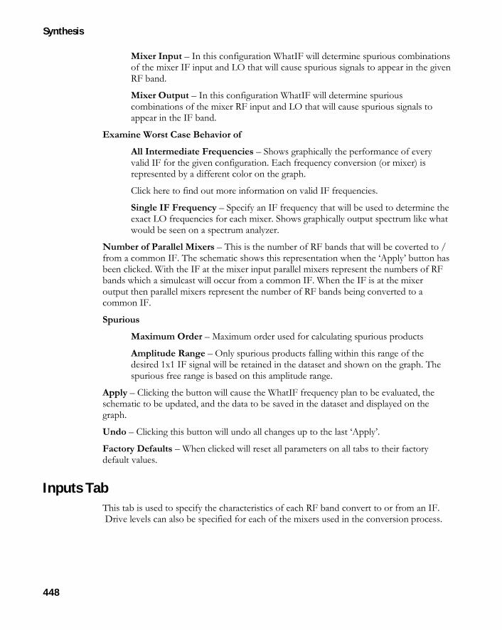
Synthesis
448
Mixer Input – In this configuration WhatIF will determine spurious combinations of the mixer IF input and LO that will cause spurious signals to appear in the given RF band.
Mixer Output – In this configuration WhatIF will determine spurious combinations of the mixer RF input and LO that will cause spurious signals to appear in the IF band.
Examine Worst Case Behavior of All Intermediate Frequencies – Shows graphically the performance of every valid IF for the given configuration. Each frequency conversion (or mixer) is represented by a different color on the graph.
Click here to find out more information on valid IF frequencies.
Single IF Frequency – Specify an IF frequency that will be used to determine the exact LO frequencies for each mixer. Shows graphically output spectrum like what would be seen on a spectrum analyzer.
Number of Parallel Mixers – This is the number of RF bands that will be coverted to / from a common IF. The schematic shows this representation when the ‘Apply’ button has been clicked. With the IF at the mixer input parallel mixers represent the numbers of RF bands which a simulcast will occur from a common IF. When the IF is at the mixer output then parallel mixers represent the number of RF bands being converted to a common IF.
Spurious Maximum Order – Maximum order used for calculating spurious products
Amplitude Range – Only spurious products falling within this range of the desired 1x1 IF signal will be retained in the dataset and shown on the graph. The spurious free range is based on this amplitude range.
Apply – Clicking the button will cause the WhatIF frequency plan to be evaluated, the schematic to be updated, and the data to be saved in the dataset and displayed on the graph.
Undo – Clicking this button will undo all changes up to the last ‘Apply’.
Factory Defaults – When clicked will reset all parameters on all tabs to their factory default values.
Inputs Tab This tab is used to specify the characteristics of each RF band convert to or from an IF. Drive levels can also be specified for each of the mixers used in the conversion process.
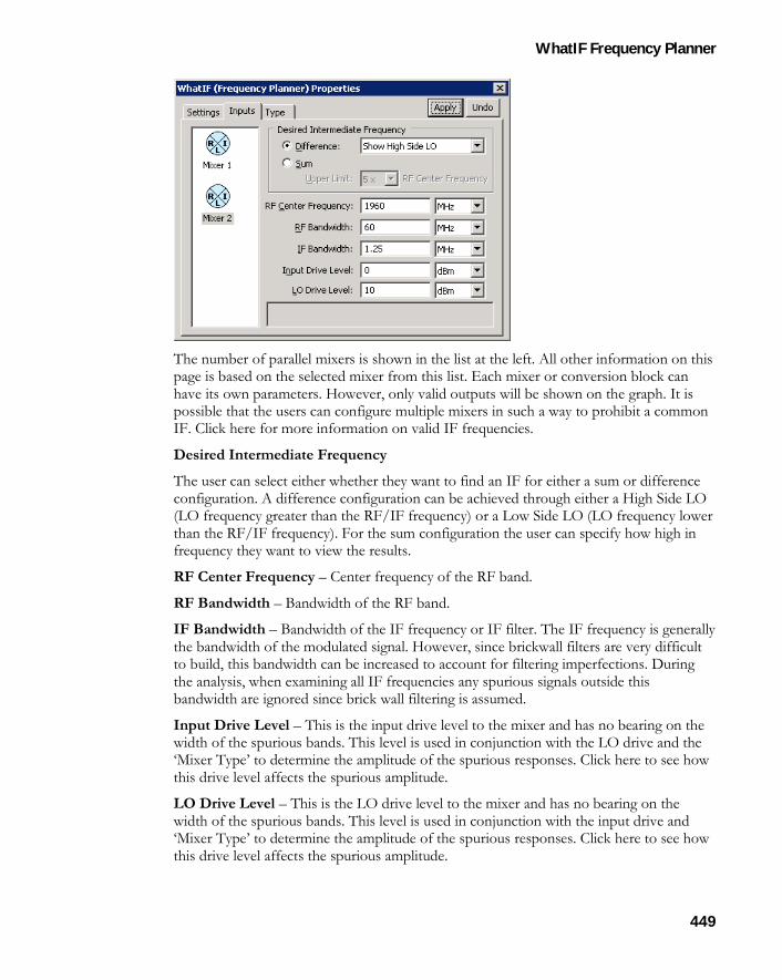
WhatIF Frequency Planner
449
The number of parallel mixers is shown in the list at the left. All other information on this page is based on the selected mixer from this list. Each mixer or conversion block can have its own parameters. However, only valid outputs will be shown on the graph. It is possible that the users can configure multiple mixers in such a way to prohibit a common IF. Click here for more information on valid IF frequencies.
Desired Intermediate Frequency The user can select either whether they want to find an IF for either a sum or difference configuration. A difference configuration can be achieved through either a High Side LO (LO frequency greater than the RF/IF frequency) or a Low Side LO (LO frequency lower than the RF/IF frequency). For the sum configuration the user can specify how high in frequency they want to view the results.
RF Center Frequency – Center frequency of the RF band.
RF Bandwidth – Bandwidth of the RF band.
IF Bandwidth – Bandwidth of the IF frequency or IF filter. The IF frequency is generally the bandwidth of the modulated signal. However, since brickwall filters are very difficult to build, this bandwidth can be increased to account for filtering imperfections. During the analysis, when examining all IF frequencies any spurious signals outside this bandwidth are ignored since brick wall filtering is assumed.
Input Drive Level – This is the input drive level to the mixer and has no bearing on the width of the spurious bands. This level is used in conjunction with the LO drive and the ‘Mixer Type’ to determine the amplitude of the spurious responses. Click here to see how this drive level affects the spurious amplitude.
LO Drive Level – This is the LO drive level to the mixer and has no bearing on the width of the spurious bands. This level is used in conjunction with the input drive and ‘Mixer Type’ to determine the amplitude of the spurious responses. Click here to see how this drive level affects the spurious amplitude.
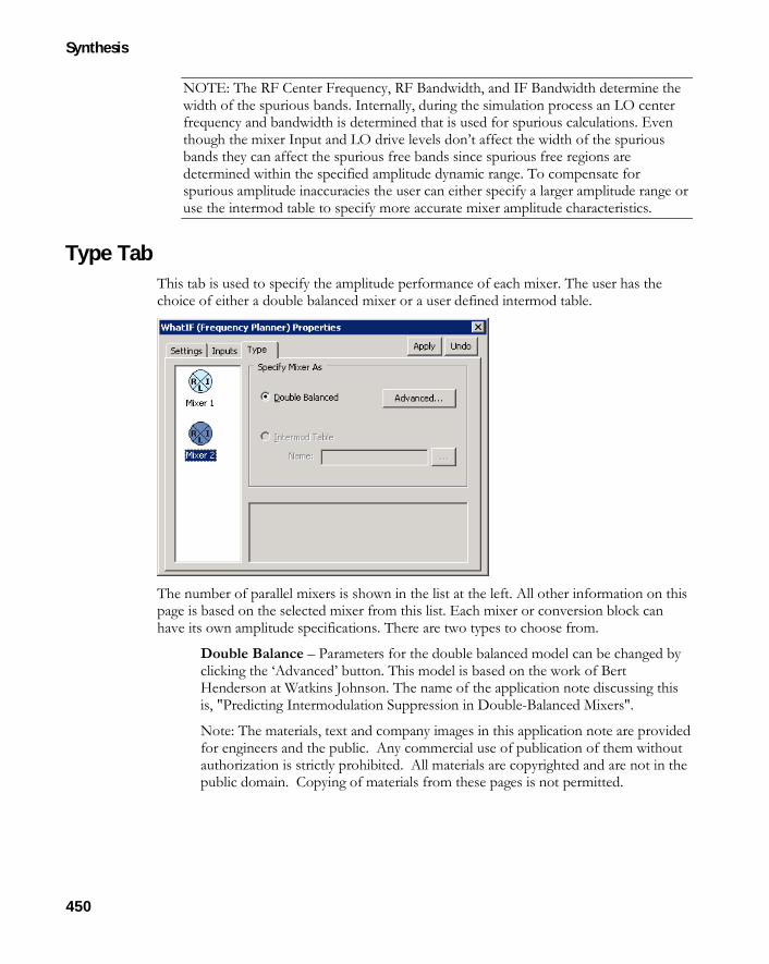
Synthesis
450
NOTE: The RF Center Frequency, RF Bandwidth, and IF Bandwidth determine the width of the spurious bands. Internally, during the simulation process an LO center frequency and bandwidth is determined that is used for spurious calculations. Even though the mixer Input and LO drive levels don’t affect the width of the spurious bands they can affect the spurious free bands since spurious free regions are determined within the specified amplitude dynamic range. To compensate for spurious amplitude inaccuracies the user can either specify a larger amplitude range or use the intermod table to specify more accurate mixer amplitude characteristics.
Type Tab This tab is used to specify the amplitude performance of each mixer. The user has the choice of either a double balanced mixer or a user defined intermod table.
The number of parallel mixers is shown in the list at the left. All other information on this page is based on the selected mixer from this list. Each mixer or conversion block can have its own amplitude specifications. There are two types to choose from.
Double Balance – Parameters for the double balanced model can be changed by clicking the ‘Advanced’ button. This model is based on the work of Bert Henderson at Watkins Johnson. The name of the application note discussing this is, "Predicting Intermodulation Suppression in Double-Balanced Mixers".
Note: The materials, text and company images in this application note are provided for engineers and the public. Any commercial use of publication of them without authorization is strictly prohibited. All materials are copyrighted and are not in the public domain. Copying of materials from these pages is not permitted.
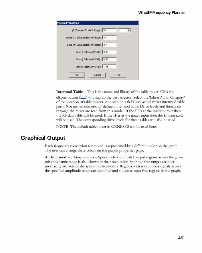
WhatIF Frequency Planner
451
Intermod Table – This is the name and library of the table mixer. Click the ellipsis button ( ) to bring up the part selector. Select the 'Library' and 'Category' of the location of table mixers. At noted, this field uses actual mixer intermod table parts. Not just an numerically defined intermod table. Drive levels and directions through the mixer are read from this model. If the IF is at the mixer output then the RF data table will be used. If the IF is at the mixer input then the IF data table will be used. The corresponding drive levels for those tables will also be used.
NOTE: The default table mixer in GENESYS can be used here.
Graphical Output Each frequency conversion (or mixer) is represented by a different color on the graph. The user can change these colors on the graphs properties page.
All Intermediate Frequencies – Spurious free and valid output regions across the given mixer dynamic range is also shown in their own color. Spurious free ranges are post processing artifacts of the spurious calculations. Regions with no spurious signals across the specified amplitude range are identified and shown as spur free regions in the graphs.

Synthesis
452
Single IF Frequency – The valid output region across the given mixer dynamic range is also shown in its own color. The graph shows a spectrum analyzer view showing the given mixer output frequency with its bandwidth along with any spurious frequencies that may appear in the output spectrum. One way to think of the spurious responses for this graph is that if the mixer input signal is swept across its input range and the LO is swept across its range the spurious signals would track the shown frequencies ranges. At the top of the graph a 1x1 spur can be seen. Remember, that the desired output will only occur at the single output frequency plus its bandwidth. However, if the input were to be swept across its entire range and the LO was swept across its entire range this would produce a 1x1 output, which covers a much larger range than the single IF frequency as shown on the graph.

WhatIF Frequency Planner
453
Flyover Help – The user can place the mouse cursor over any object in the graph to get information about the given spurious band or region. For spurious free or valid IF regions the information is self explanatory. For spurious bands in the ‘Performance of All IF’s’ case the information is as follows. In the 1st line the given mixer is identified (this can also be determined by its trace color). Next the given spurious combination along with the corresponding input ports are given. In the following example the spurious band is -1 x RF and -2 x LO. The LO frequency is given on the 2nd line of the flyover help. The 3rd line contains the spurious band where this spurious combination would fall at any IF frequency selected in this range. The 4th line contains the amplitude of the spurious signal relative to the IF power output level of 0 dBc. In the following example any IF frequency between 281.542 and 306.125 MHz would have a -1x-2 spur at the given amplitude of -32.12 dBc.
Using the flyover help information the user can manually verify the analysis is giving the correct results. The flyover information must be used in conjunction with the mixer configuration to determine the spurious frequency. For example, given the above flyover help we can determine the IF frequency range by considering the mixer configuration for ‘Mixer#1’. Since this is a difference mixer with a low side LO then the IF equation is IF = RF - LO. Substituting in the flyover help information we would get an IF center frequency spurious of -1 x RF - ( -2 x LO ). Using actual values we get IF Center Frequency = -1 x 881.5 MHz (RF Center Frequency for Mixer#1) - ( -2 x 587.667 MHz ) = 293.834 MHz. This frequency is the center of the 281.542 and 306.125 MHz band. Once we account for the RF and IF bandwidths we can estimate the entire spur band. The exact calculations of the band ends are more complicated that this is proprietary information.
Click here for information about mixer configuration equations.
Configuration Equations Mixer Configuration Equations
IF at the mixer output Difference, Low Side LO: IF = RF – LO.
Difference, High Side LO: IF = LO – RF.
Sum: IF = RF + LO.
IF at the mixer input Difference, IF < LO: RF = IF – LO.
Synthesis
454
Difference, LO > IF: RF = LO – IF.
Sum: RF = IF + LO.
Mixer Drive Levels Mixer input (RF/IF) drive levels are used to determine the amplitude of the spurious responses. These levels have no effect on the widths (frequency ranges) of the spurious bands that are generated by WhatIF. The widths of these spurious bands are controlled by the RF Center Frequency, RF Bandwidth, IF Bandwidth, and mixer configuration (sum, difference low side LO, or difference high side LO). The LO signal is used to turn the mixer on and off. The mixer input (RF/IF) is mixed with its harmonics with the harmonics of the LO as shown by the following equation.
FIF = m x FRF ± n x FLO or FRF = m x FIF ± n x FLO
m = 0, 1, 2, …
n = 0, 1, 2, …
FIF = IF frequency
FRF = any frequency in the RF band
FLO = any frequency in the LO band
Theoretically, the 'm x FRF' or 'm x FIF' products will decrease (m-1) dB for each dB the input power (RF or IF) is decreased. Obviously, the lower the input drive level to the mixer the more linear it will be and the lower the spurious responses are.
Valid IF Frequencies Valid IF frequencies are based on the mixer configuration equations. Valid IF frequencies are those frequencies whose equations will give a positive frequency result. For example, if we were trying to find an IF for a sum mixer with the IF at the input (RF = IF + LO) then by definition the IF frequency must be below the RF band. No valid IF frequencies could exist for a sum output where the IF frequency was greater than the RF frequency. If the user wants an IF frequency greater than the RF band for this configuration then a difference mixer must be selected. In the above example (RF = IF + LO) the maximum IF could be equal to the RF frequency if the LO was 0 Hz. The minimum IF frequency would be 0 Hz. Consequently, valid IF frequencies for this configuration would be between 0 Hz and the lowest RF frequency.
For difference mixer configurations where the IF is at the mixer output then IF frequencies will always be below the RF band. For difference mixer configurations where the IF is at the mixer input then valid IF frequencies will be greater than the RF band.
In the parallel mixer case then the intersection of valid frequencies for all mixers will be shown on the graph. For example, one mixer could have a sum configuration and another could have a difference configuration. Only the IF frequencies that satisfy both of these
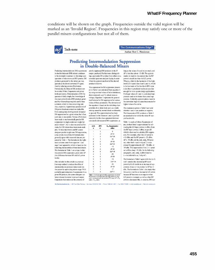
WhatIF Frequency Planner
455
conditions will be shown on the graph. Frequencies outside the valid region will be marked as an ‘Invalid Region’. Frequencies in this region may satisfy one or more of the parallel mixers configurations but not all of them.
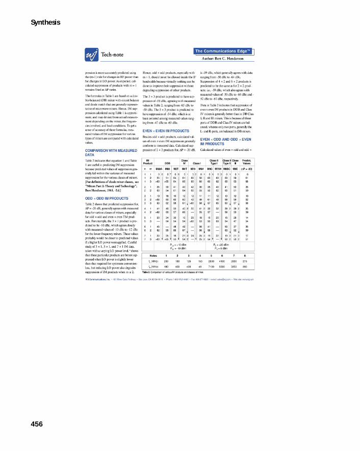
Synthesis
456
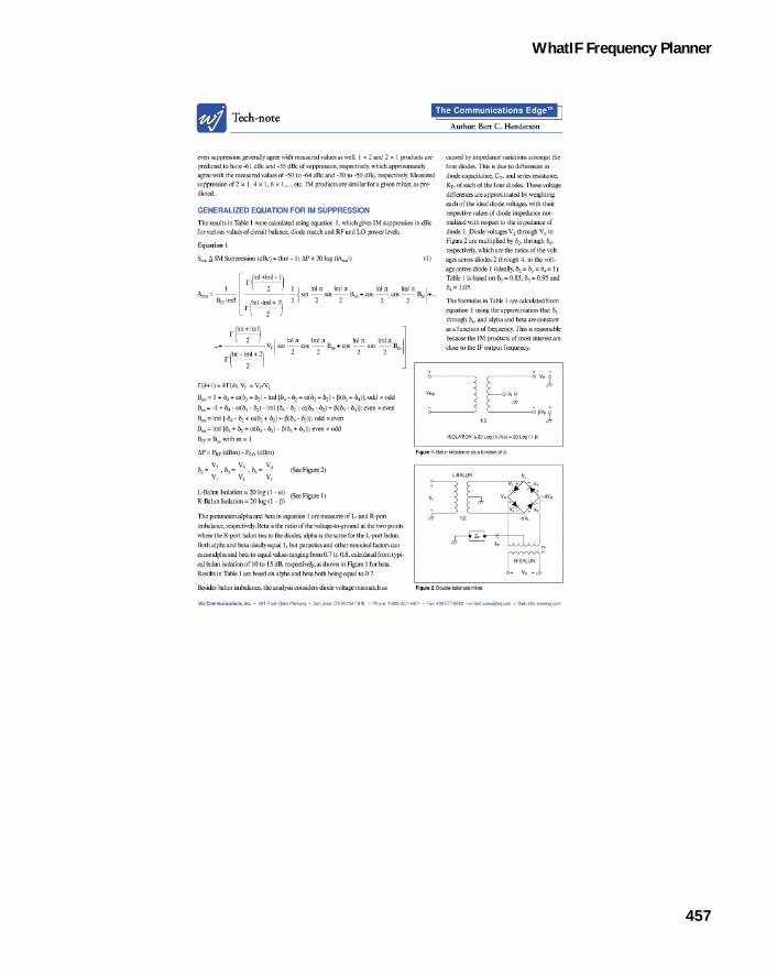
WhatIF Frequency Planner
457
Synthesis
458

WhatIF Frequency Planner
459
Synthesis
460
461
Chapter 14: Filter Shapes
Filter Shapes Overview
Note: This section of the GENESYS documentation contains information for all filter synthesis programs, including FILTER, A/FILTER, M/FILTER, and S/FILTER.
For each filter type such as lowpass, bandpass, etc. there are a number of response shapes. The design of all filters is based on a lowpass filter with that shape of response. This lowpass filter is called the lowpass prototype and the values of elements in that filter are called the prototype “G” values. The values are normalized to 1 ohm input impedance and a cutoff frequency of 1 radian/sec [1].
To design a filter, FILTER computes these prototype values, makes the transformation to the desired type and normalizes to the specified impedances and frequencies.
FILTER computes the prototype G values for Butterworth, Bessel, Chebyshev, singly-equalized delay and elliptic Cauer-Chebyshev shapes. Also FILTER allows storing of frequently used prototype G values in disk files which are automatically read to design other filter responses. Included with GENESYS are lowpass prototype G values for several different filter responses. The included response types are discussed later in this chapter. Other lowpass prototype files may be entered by the user using the editor in GENESYS.
Dozens of tables of prototype G values have been published through the years for specific applications, and more may be expected in the future. Many tables of values are given in the references cited in this manual.
Butterworth The Butterworth lowpass response is useful when match and delay in the passband, particularly low frequencies, are important. The shape is characterized by monotonically increasing attenuation in the pass band to 3 dB at the cutoff frequency. Attenuation monotonically increases with increasing frequency in the transition and stopbands. Filters with infinite attenuation only at DC or infinite frequency, and therefore which have no zeros of transmission at finite frequencies, are called all-pole filters.
The Butterworth is a simple filter, with suitable characteristics for many applications. For straightforward filtering applications, the Butterworth is the filter response of choice. Its disadvantage is only fair selectivity. The frequency response of the Butterworth lowpass filter is given by:
Atten = 10 LOG10[1 + (f/fc)2N] dB
Synthesis
462
where
f = frequency fc= 3 dB cutoff N = order
The equations used in GENESYS to compute the lowpass prototype G values for the Butterworth filter are given in reference [2].
The output impedance of the Butterworth lowpass prototype filter is equal to the input impedance, therefore G(0), the first prototype G value, is equal to G(N+1), the last prototype G value.
The normal definition for the cutoff of Butterworth filters is the 3 dB attenuation frequency. GENESYS allows the user to specify the desired attenuation at the requested cutoff frequency. For example, the user may specify a cutoff frequency at 1 dB attenuation. Any cutoff attenuation greater than zero may be specified for the Butterworth response.
Chebyshev The Chebyshev lowpass response is characterized by equal attenuation ripple in the passband, with attenuation equal to the ripple at the cutoff frequency. The Chebyshev is an all-pole filter. The Chebyshev filter gives better selectivity than the Butterworth filter. The Chebyshev filter is an excellent choice when passband attenuation and return loss ripple can be tolerated. The frequency response of the Chebyshev lowpass filter above cutoff is given by:
Atten = 10 LOG101+e cosh2[N cosh-1(f/fc)] dB
where
f = frequency fc= 3 dB cutoff N = order e = 10RIPPLE/10 - 1
The equations used in GENESYS to compute the lowpass prototype G values for the Chebyshev filter are given in reference [2].
The output impedance for Chebyshev prototype filters of odd order are equal to the input impedance, therefore G(0), the first prototype G value is equal to G(N+1), the last prototype G value.
For even order Chebyshev prototype filters, the output impedance is less than or greater than the input impedance, depending on whether the subtype is ML or MC. The difference is related to the passband ripple and is greater for larger passband ripple.
GENESYS automatically determines and displays the output impedance.
Two normal definitions for the cutoff of Chebyshev filters are often used. Some contributors have defined the cutoff attenuation as 3 dB, and others define the cutoff
Filter Shapes
463
attenuation as the passband ripple value, with the latter perhaps somewhat more generally accepted. We will define the cutoff attenuation as the ripple value. However, GENESYS allows the user to specify any attenuation equal to or greater than the ripple attenuation as the cutoff. For example, the user may specify a cutoff frequency for a .25 dB ripple Chebyshev at .25, 1.07, 3, 6 dB, etc. attenuation. Any cutoff attenuation greater than the ripple may be specified for the Chebyshev response.
Bessel The Bessel filter produces a maximally flat group delay in the frequency domain. It is sometimes referred to as a maximally flat group delay filter and sometimes as a Thompson filter.
Maximally flat group delay is often an advantage in pulse communication system applications. This filter has excellent characteristics in the time domain.
The disadvantage is extremely poor selectivity. However, for applications where good phase or time domain performance is critical, it is often the best choice.
GENESYS will design Bessel filters through 10th order.
Blinchikoff Flat Delay Bandpass Transformation of lowpass filters to bandpass filters results in the modification of the group delay characteristics of the lowpass prototype. Consequently, bandpass filters designed using Bessel, minimum phase equiripple error and other controlled delay prototypes do not exhibit the desired delay characteristics. This phenomenon worsens with increasing bandpass filter bandwidth. Some transform types, such as the top-C coupled bandpass, are worse than others, such as the shunt-C coupled bandpass. The reasons for this phenomena is discussed in the EQUALIZE documentation.
Blinchikoff and Savetman [3][4] offered a solution to this dilemma for 2nd and 4th order all-pole filters. The poles of the transfer function were optimized by computer for constant delay over the passband directly as a bandpass filter. The lowpass to bandpass transform is therefore avoided. The process is not numerically efficient, but the effort provides a useful set of constant delay bandpass filters for 30 to 70% bandwidth.
The extremely desirable delay characteristics of a 4th order Blinchikoff bandpass filter with 40% bandwidth centered at 70 MHz are demonstrated in the accompanying response. As might be expected, the amplitude selectivity characteristics of the filter are poor.
Singly Equalized Delay All ladder, passive, filter structures are minimum-phase; the amplitude and phase responses are inseparably related via the Hilbert transform. Selectivity and flat delay cannot be simultaneously achieved.
Synthesis
464
To resolve this difficulty, selective filters are sometimes cascaded with non-ladder all-pass delay equalization networks. Unfortunately several all-pass sections may be required and each requires several components.
Developed by Eagleware, the singly-equalized prototype offers selectivity far better than Bessel and other controlled phase prototypes but it is perfectly delay equalized with a single all-pass network. This prototype may be selected from the Shape dialog box. The theory behind the development of these prototypes is described as an example in HF Filter Design and Computer Simulation.
Singly-Terminated Sometimes a filter which is singly-terminated is required. =FILTER= will design Butterworth and Chebyshev filters terminated on the input with a specified impedance and terminated on the output with either zero or an infinite impedance. The input and output of these filters may be swapped. Other filter shapes may be designed for single termination by user or file entry of the lowpass prototype G values. The Help screen in the Shape subwindow may be used to determine which subtype for a given filter type will have an infinite or a zero output impedance.
Since singly-terminated filters are not really matching networks, the insertion loss of these filters is not 0 dB in the passband. Consider a lowpass filter consisting of series inductors and shunt capacitors inserted between a source of 50 ohms and a zero impedance load. As the frequency approaches zero, the capacitors effectively become open circuits and the inductors effectively disappear. How can these components match the source to the load if they are effectively absent? The answer is they can not. Singly-terminated filters preserve the shape of the amplitude response and the shape of the voltage response, but when the power transferred between the source and load is calculated or measured, the insertion loss is proportional to the difference in input and output impedances.
When writing GENESYS schematics for singly-terminated filters in order to avoid infinite attenuation in the calculated loss of the passband, FILTER sets the output impedance at 398 or 1/398 times the input impedance, instead of infinity or zero. The response of a filter changes little when the ratio is greater than about 20. The ratio of 398 results in an attenuation offset of approximately 20 dB, so singly-terminated filters analyzed using GENESYS require adding a 20 dB offset to the scale of S21 and S12.
Cauer-Chebyshev Elliptic function filters have zeros of transmission at finite as well as infinite frequencies. Zeros of transmission at finite frequencies can reduce the width of the transition region, therefore increasing the selectivity or “sharpness” of the response. An important class of elliptic function filters is the Cauer-Chebyshev, which exhibits equiripple passbands and equal minimum attenuation, Amin, in the stopband. GENESYS designs Cauer-Chebyshev filters with user specified passband ripple and stopband ripple. These routines are based on work by Pierre Amstutz [5]. In the Amstutz paper, distinctly different routines were given for even and odd order Cauer-Chebyshev prototype filters. The routines used
Filter Shapes
465
different input data for determining values in the odd or even case. The GENESYS routines remove this disadvantage.
GENESYS computes prototype G values for both type B and type C Cauer-Chebyshev filters:
• Type B Cauer-Chebyshev filters are similar to Chebyshev filters in that the input and output impedances for even order are dissimilar.
• Type C filters approximate the filter response for equal input and output impedances for even order. The selectivity suffers slightly for type C, but this is a minor inconvenience when equal input and output impedance is required.
User Filters The powerful optimizing routines in GENESYS can be used to develop prototype G values with a limitless variety of amplitude or delay characteristics. An example of using GENESYS to develop a new lowpass prototype class is given in the Examples manual.
G(0) is the normalized input impedance. It is normally 1. For all-pole filters, G(1) through G(N) are the prototype values, and G(N+1) is the normalized output impedance.
For elliptic filters designed by GENESYS, the number of finite frequency zeros of the lowpass prototype, M is given by:
For N odd,
M = .5(N-1)
and for N even,
M = .5(N-2)
There are N+M prototype G values for elliptic filters. The normalized output impedance is G(N+M+1). The form of the elliptic lowpass prototype filter is given on the previous page. For even order filters, the final series branch is non-elliptic. The Cauer-Chebyshev and many other elliptic function filters utilize this topology. The general case for filters with zeros of transmission at finite frequencies may not utilize this topology. For example, the older class of m-derived filters have designer selected topologies.
Prototype Files Some frequently used prototype G values have been supplied with =FILTER=. These files have the same format as files which you manually create. The form of these files is:
Remark line describes type and must be included. 3 1 1 2 1 1 4 1 0.7654 1.848 1.848 0.7654 1 5 1 0.618 1.618 2 1.618 0.618 1 7 1 0.445 1.247 1.802 2 1.802 1.247 0.445 1
This particular file is for Butterworth prototype filters of 3rd through 5th and 7th order.
The remark line is used to describe the type of lowpass prototype for reference. The remark line must be present. One line of data is used for each order. One or more orders

Synthesis
466
may be in a file. The first number in a line is the order. The second number is G(0), the third G(1), etc. up to G(N+1), or up to G(N+M+1) for elliptic function filters.
When reading a file, if a data line for the specified filter order is not found, the message “Data for order N not found in file.” is displayed. Either edit the file or specify a new one. An incorrect number of data points in a line of data adversely effects program operation so please carefully check prototype files you create.
We recommend using the extension “.PRO” for all-pole lowpass prototype files and the extension “.PRE” for elliptic lowpass prototype files you create.
Included Prototype Files To begin your collection of special purpose lowpass prototype filters kept as files, the =FILTER= disk contains a number of lowpass prototype files. Included are:
• Linear phase 0.05 degree equiripple error: orders 2-10.
• Linear phase 0.5 degree equiripple error: orders 2-10.
• Transitional Gaussian to 6 dB: orders 3-8.
• Transitional Gaussian to 12 dB: orders 3-8.
• Singly-terminated Cauer-Chebyshev: orders 3-7. (Ripple = 72 dB which is 24 files.)
• Bessel passband elliptic: orders 3-4 for Amin = 18, 24: orders 3-8 for Amin = 34, 42, 50, 58, 66, 70 dB.
The prototype files except Bessel passband elliptic are provided with permission from reference [1], Handbook of Filter Synthesis, by Anatol I Zverev, published by John Wiley and Sons. This reference includes many other singly-terminated Cauer-Chebyshev prototypes and other useful lowpass prototypes.
The Bessel passband elliptic stopband lowpass prototypes are provided with permission from reference [6], Electronic Filter Design Handbook, by Arthur B. Williams and Fred J. Taylor, published by McGraw-Hill.
Linear Phase Equripple Error Just as the Chebyshev prototypes are an optimum amplitude response solution, the linear phase prototypes are an optimum linear phase solution (constant group delay) given an allowable phase ripple. By allowing some phase ripple, improved selectivity is obtained. The two prototype files are named “LP0R05.PRO” and “LP0R5.PRO”. LP is an acronym for linear phase. 0R05 and 0R5 represent respectively 0.05 and 0.5 degrees phase ripple.
Filter Shapes
467
Transitional Gaussian Also included are Gaussian to 6 dB (G06.PRO) and Gaussian to 12 dB (G12.PRO) transitional lowpass prototype filters for 3rd through 8th order. This class of filter approximates a Gaussian response to 6 or 12 dB and is a compromise of delay and selectivity characteristics.
Both the linear phase equiripple error and transitional Gaussian prototypes are doubly-terminated unsymmetrical filters. The component values on the input and output are not mirror images of each other.
Singly Terminated Cauer-Chebyshev GENESYS synthesizes doubly-terminated Cauer-Chebyshev elliptic functions directly. However, it does not synthesize singly-terminated Cauer-Chebyshev functions. This class is useful for designing contiguous elliptic diplex filters, so a number of prototype files for this class are included on disk.
The convention for naming these files is CCnNPPAA, where CC represents Cauer-Chebyshev, nN are the lowest and highest order included, PP is the reflection coefficient in percent, and AA is the approximate Amin in decibels. For the most part, the orders included are 3rd through 7th. The reflection coefficients are 1, 2, 4, 8, 10, 15, 20, and 25%, which represents a passband ripple of .00043, .0017, .007, .028, .044, .098, .18 and .28 dB respectively. Reference [1], which was so popular it has gone back into print, contains many other prototype files.
Bessel Passband Elliptic Stopband As was discussed previously, Bessel filters have excellent delay characteristics, but poor selectivity. The selectivity of flat delay filters can be improved by adding zeros of transmission at finite frequencies. Elliptic lowpass prototypes for such a class of filters is given in reference [6]. The amplitude and delay responses for 5th order Bessel (solid curves) and elliptic Bessel Amin =50 dB (dotted curves) filters with 1 MHz cutoffs are compared in the accompanying figure.
Order Help FILTER, A/FILTER, and M/FILTER can help you determine the order required for Butterworth, Chebyshev and elliptic Cauer-Chebyshev filters.
Suppose you need a bandpass filter which passes 10.5 to 10.9 MHz with a maximum ripple of .1 dB. The rejection at 10.2 MHz and 11.2 MHz must be at least 50 dB. We will determine the minimum order required for a Chebyshev and a Cauer-Chebyshev filter.
Select "Order Help" from the Settings tab. Determine the Chebyshev order first. Select the Bandpass and Chebyshev radio buttons. Enter “.1" for the ripple prompt. Enter ”10.5" and “10.9" for the Fl and Fu prompts respectively.
Synthesis
468
You may then enter up to 10 separate stopband requirements. =FILTER= will automatically determine which requirement is the most stringent and compute the necessary order based on that requirement. In this case, at the F0 and A0 prompts, enter “10.2" and ”50". At the next F1 and A1 prompts enter “11.2" and ”50". When you are finished entering stopband requirements, enter “0". The necessary order is computed and displayed as 5.39. The filter is therefore designed with the next higher integer order of 6.
Next, determine the necessary order for a Cauer-Chebyshev elliptic bandpass filter. Select the Cauer-Chebyshev radio button. Enter “50" at the prompt Amin, ”10.5" at the Fl prompt and “10.9" at the Fu prompt.
For Cauer-Chebyshev bandpass filters, only two stopband requirements are entered, because the required stopband attenuation is assumed equal to Amin. Enter the lower and upper stopband requirements closest in frequency to the passband. For elliptic lowpass filters, only one stopband requirement is used.
Therefore, enter “10.2" at the Fsl prompt and ”11.2" at the Fsu prompt. The required order is 4.03. Because this is very close to 4, a 4th order filter might be chosen. Re-running N-Help with Amin of 49 dB gives a required order of 3.98, so you know that a 4th order filter will have between 49 and 50 dB of attenuation.
Select the close button to return to the main window.
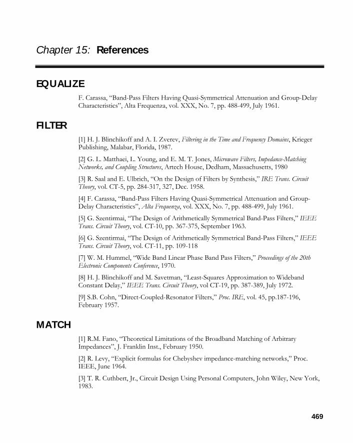
469
Chapter 15: References
EQUALIZE F. Carassa, “Band-Pass Filters Having Quasi-Symmetrical Attenuation and Group-Delay Characteristics”, Alta Frequenza, vol. XXX, No. 7, pp. 488-499, July 1961.
FILTER [1] H. J. Blinchikoff and A. I. Zverev, Filtering in the Time and Frequency Domains, Krieger Publishing, Malabar, Florida, 1987.
[2] G. L. Matthaei, L. Young, and E. M. T. Jones, Microwave Filters, Impedance-Matching Networks, and Coupling Structures, Artech House, Dedham, Massachusetts, 1980
[3] R. Saal and E. Ulbrich, “On the Design of Filters by Synthesis,” IRE Trans. Circuit Theory, vol. CT-5, pp. 284-317, 327, Dec. 1958.
[4] F. Carassa, “Band-Pass Filters Having Quasi-Symmetrical Attenuation and Group-Delay Characteristics”, Alta Frequenza, vol. XXX, No. 7, pp. 488-499, July 1961.
[5] G. Szentirmai, “The Design of Arithmetically Symmetrical Band-Pass Filters,” IEEE Trans. Circuit Theory, vol. CT-10, pp. 367-375, September 1963.
[6] G. Szentirmai, “The Design of Arithmetically Symmetrical Band-Pass Filters,” IEEE Trans. Circuit Theory, vol. CT-11, pp. 109-118
[7] W. M. Hummel, “Wide Band Linear Phase Band Pass Filters,” Proceedings of the 20th Electronic Components Conference, 1970.
[8] H. J. Blinchikoff and M. Savetman, “Least-Squares Approximation to Wideband Constant Delay,” IEEE Trans. Circuit Theory, vol CT-19, pp. 387-389, July 1972.
[9] S.B. Cohn, “Direct-Coupled-Resonator Filters,” Proc. IRE, vol. 45, pp.187-196, February 1957.
MATCH [1] R.M. Fano, “Theoretical Limitations of the Broadband Matching of Arbitrary Impedances”, J. Franklin Inst., February 1950.
[2] R. Levy, “Explicit formulas for Chebyshev impedance-matching networks,” Proc. IEEE, June 1964.
[3] T. R. Cuthbert, Jr., Circuit Design Using Personal Computers, John Wiley, New York, 1983.
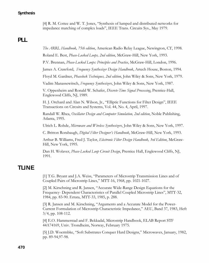
Synthesis
470
[4] R. M. Cottee and W. T. Jones, “Synthesis of lumped and distributed networks for impedance matching of complex loads”, IEEE Trans. Circuits Sys., May 1979.
PLL The ARRL Handbook, 75th edition, American Radio Relay League, Newington, CT, 1998.
Roland E. Best, Phase-Locked Loops, 2nd edition, McGraw-Hill, New York, 1993.
P.V. Brennan, Phase-Locked Loops: Principles and Practice, McGraw-Hill, London, 1996.
James A. Crawford, Frequency Synthesizer Design Handbook, Artech House, Boston, 1994.
Floyd M. Gardner, Phaselock Techniques, 2nd edition, John Wiley & Sons, New York, 1979.
Vadim Manassewitsch, Frequency Synthesizers, John Wiley & Sons, New York, 1987.
V. Oppenheim and Ronald W. Schafer, Discrete-Time Signal Processing, Prentice-Hall, Englewood Cliffs, NJ, 1989.
H. J. Orchard and Alan N. Wilson, Jr., “Elliptic Functions for Filter Design”, IEEE Transactions on Circuits and Systems, Vol. 44, No. 4, April, 1997.
Randall W. Rhea, Oscillator Design and Computer Simulation, 2nd edition, Noble Publishing, Atlanta, 1995.
Ulrich L. Rohde, Microwave and Wireless Synthesizers, John Wiley & Sons, New York, 1997.
C. Britton Rorabaugh, Digital Filter Designer’s Handbook, McGraw-Hill, New York, 1993.
Arthur B. Williams, Fred J. Taylor, Electronic Filter Design Handbook, 3rd Edition, McGraw-Hill, New York, 1995.
Dan H. Wolaver, Phase-Locked Loop Circuit Design, Prentice Hall, Englewood Cliffs, NJ, 1991.
TLINE [1] T.G. Bryant and J.A. Weiss, “Parameters of Microstrip Transmission Lines and of Coupled Pairs of Microstrip Lines,” MTT-16, 1968, pp. 1021-1027.
[2] M. Kirschning and R. Jansen, “Accurate Wide-Range Design Equations for the Frequency- Dependent Characteristics of Parallel Coupled Microstrip Lines”, MTT-32, 1984, pp. 83-90. Errata, MTT-33, 1985, p. 288.
[3] R. Jansen and M. Kirschning, “Arguments and a Accurate Model for the Power-Current Formulation of Microstrip Characteristic Impedance,” AEU, Band 37, 1983, Heft 3/4, pp. 108-112.
[4] E.O. Hammerstad and F. Bekkadal, Microstrip Handbook, ELAB Report STF 44A74169, Univ. Trondheim, Norway, February 1975.
[5] J.D. Woermbke, “Soft Substrates Conquer Hard Designs,” Microwaves, January, 1982, pp. 89-94,97-98.
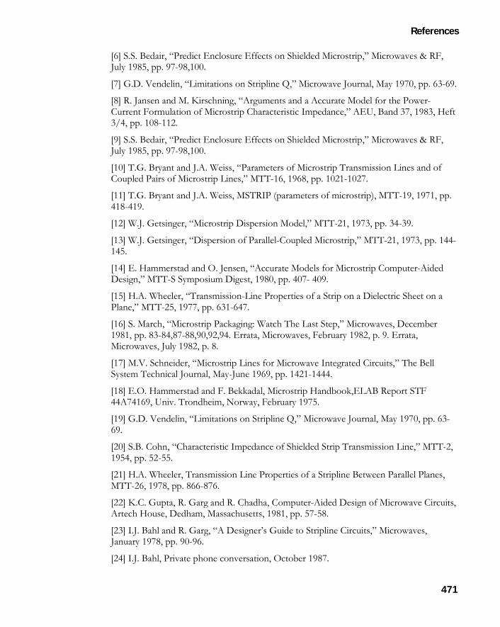
References
471
[6] S.S. Bedair, “Predict Enclosure Effects on Shielded Microstrip,” Microwaves & RF, July 1985, pp. 97-98,100.
[7] G.D. Vendelin, “Limitations on Stripline Q,” Microwave Journal, May 1970, pp. 63-69.
[8] R. Jansen and M. Kirschning, “Arguments and a Accurate Model for the Power-Current Formulation of Microstrip Characteristic Impedance,” AEU, Band 37, 1983, Heft 3/4, pp. 108-112.
[9] S.S. Bedair, “Predict Enclosure Effects on Shielded Microstrip,” Microwaves & RF, July 1985, pp. 97-98,100.
[10] T.G. Bryant and J.A. Weiss, “Parameters of Microstrip Transmission Lines and of Coupled Pairs of Microstrip Lines,” MTT-16, 1968, pp. 1021-1027.
[11] T.G. Bryant and J.A. Weiss, MSTRIP (parameters of microstrip), MTT-19, 1971, pp. 418-419.
[12] W.J. Getsinger, “Microstrip Dispersion Model,” MTT-21, 1973, pp. 34-39.
[13] W.J. Getsinger, “Dispersion of Parallel-Coupled Microstrip,” MTT-21, 1973, pp. 144-145.
[14] E. Hammerstad and O. Jensen, “Accurate Models for Microstrip Computer-Aided Design,” MTT-S Symposium Digest, 1980, pp. 407- 409.
[15] H.A. Wheeler, “Transmission-Line Properties of a Strip on a Dielectric Sheet on a Plane,” MTT-25, 1977, pp. 631-647.
[16] S. March, “Microstrip Packaging: Watch The Last Step,” Microwaves, December 1981, pp. 83-84,87-88,90,92,94. Errata, Microwaves, February 1982, p. 9. Errata, Microwaves, July 1982, p. 8.
[17] M.V. Schneider, “Microstrip Lines for Microwave Integrated Circuits,” The Bell System Technical Journal, May-June 1969, pp. 1421-1444.
[18] E.O. Hammerstad and F. Bekkadal, Microstrip Handbook,ELAB Report STF 44A74169, Univ. Trondheim, Norway, February 1975.
[19] G.D. Vendelin, “Limitations on Stripline Q,” Microwave Journal, May 1970, pp. 63-69.
[20] S.B. Cohn, “Characteristic Impedance of Shielded Strip Transmission Line,” MTT-2, 1954, pp. 52-55.
[21] H.A. Wheeler, Transmission Line Properties of a Stripline Between Parallel Planes, MTT-26, 1978, pp. 866-876.
[22] K.C. Gupta, R. Garg and R. Chadha, Computer-Aided Design of Microwave Circuits, Artech House, Dedham, Massachusetts, 1981, pp. 57-58.
[23] I.J. Bahl and R. Garg, “A Designer’s Guide to Stripline Circuits,” Microwaves, January 1978, pp. 90-96.
[24] I.J. Bahl, Private phone conversation, October 1987.
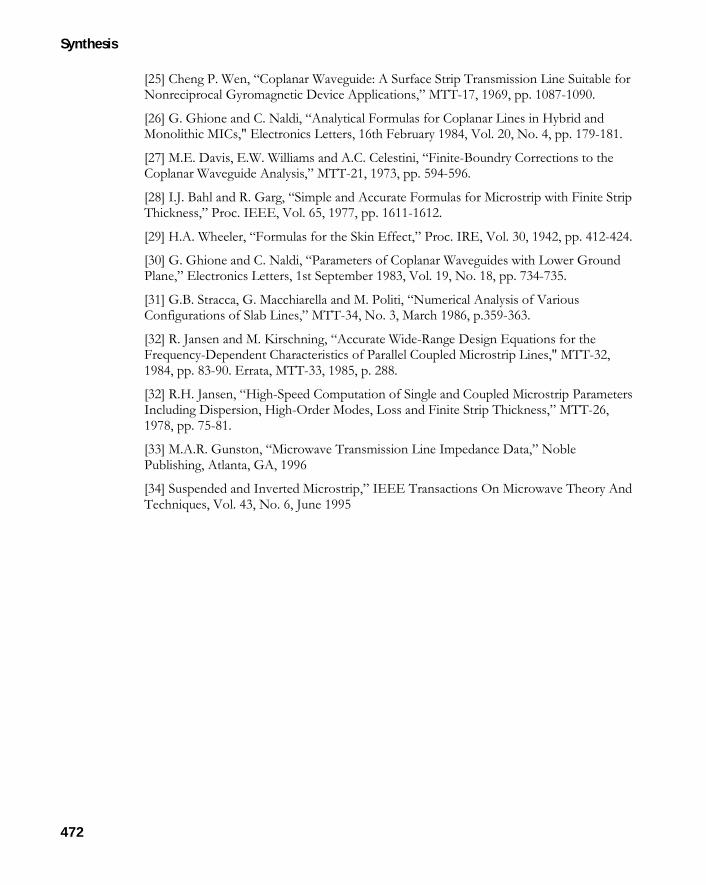
Synthesis
472
[25] Cheng P. Wen, “Coplanar Waveguide: A Surface Strip Transmission Line Suitable for Nonreciprocal Gyromagnetic Device Applications,” MTT-17, 1969, pp. 1087-1090.
[26] G. Ghione and C. Naldi, “Analytical Formulas for Coplanar Lines in Hybrid and Monolithic MICs," Electronics Letters, 16th February 1984, Vol. 20, No. 4, pp. 179-181.
[27] M.E. Davis, E.W. Williams and A.C. Celestini, “Finite-Boundry Corrections to the Coplanar Waveguide Analysis,” MTT-21, 1973, pp. 594-596.
[28] I.J. Bahl and R. Garg, “Simple and Accurate Formulas for Microstrip with Finite Strip Thickness,” Proc. IEEE, Vol. 65, 1977, pp. 1611-1612.
[29] H.A. Wheeler, “Formulas for the Skin Effect,” Proc. IRE, Vol. 30, 1942, pp. 412-424.
[30] G. Ghione and C. Naldi, “Parameters of Coplanar Waveguides with Lower Ground Plane,” Electronics Letters, 1st September 1983, Vol. 19, No. 18, pp. 734-735.
[31] G.B. Stracca, G. Macchiarella and M. Politi, “Numerical Analysis of Various Configurations of Slab Lines,” MTT-34, No. 3, March 1986, p.359-363.
[32] R. Jansen and M. Kirschning, “Accurate Wide-Range Design Equations for the Frequency-Dependent Characteristics of Parallel Coupled Microstrip Lines," MTT-32, 1984, pp. 83-90. Errata, MTT-33, 1985, p. 288.
[32] R.H. Jansen, “High-Speed Computation of Single and Coupled Microstrip Parameters Including Dispersion, High-Order Modes, Loss and Finite Strip Thickness,” MTT-26, 1978, pp. 75-81.
[33] M.A.R. Gunston, “Microwave Transmission Line Impedance Data,” Noble Publishing, Atlanta, GA, 1996
[34] Suspended and Inverted Microstrip,” IEEE Transactions On Microwave Theory And Techniques, Vol. 43, No. 6, June 1995
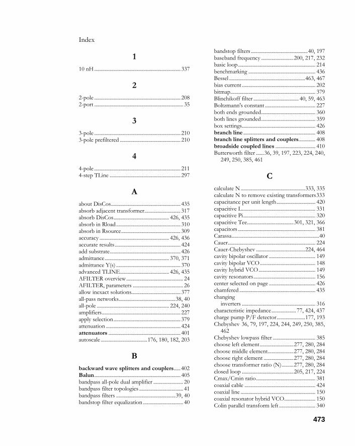
473
Index
1 10 nH ................................................................... 337
2 2-pole ................................................................... 208 2-port ..................................................................... 35
3 3-pole ................................................................... 210 3-pole prefiltered ............................................... 210
4 4-pole ................................................................... 211 4-step TLine ....................................................... 297
A about DisCos...................................................... 435 absorb adjacent transformer............................ 317 absorb DisCos........................................... 426, 435 absorb in Rload.................................................. 310 absorb in Rsource.............................................. 309 accuracy ...................................................... 426, 436 accurate results ................................................... 424 add substrate....................................................... 426 admittance.................................................. 370, 371 admittance Y(s) .................................................. 370 advanced TLINE...................................... 426, 435 AFILTER overview............................................ 24 AFILTER, parameters ....................................... 26 allow inexact solutions...................................... 377 all-pass networks............................................38, 40 all-pole ........................................................ 224, 240 amplifiers............................................................. 227 apply selection.................................................... 379 attenuation .......................................................... 424 attenuators ........................................................ 401 autoscale ....................................176, 180, 182, 203
B backward wave splitters and couplers..... 402 Balun................................................................... 405 bandpass all-pole dual amplifier ....................... 20 bandpass filter topologies .................................. 41 bandpass filters ..............................................39, 40 bandstop filter equalization ............................... 40
bandstop filters ............................................40, 197 baseband frequency .........................200, 217, 232 basic loop............................................................ 214 benchmarking .................................................... 436 Bessel ...........................................................463, 467 bias current ......................................................... 202 bitmap.................................................................. 379 Blinchikoff filter ................................... 40, 59, 463 Boltzmann's constant ....................................... 227 both ends grounded.......................................... 360 both lines grounded.......................................... 359 box settings......................................................... 426 branch line ........................................................ 408 branch line splitters and couplers............. 408 broadside coupled lines ............................... 410 Butterworth filter ......36, 39, 197, 223, 224, 240,
249, 250, 385, 461
C calculate N ..................................................333, 335 calculate N to remove existing transformers333 capacitance per unit length.............................. 420 capacitive L......................................................... 331 capacitive Pi........................................................ 320 capacitive Tee....................................301, 321, 366 capacitors ............................................................ 381 Carassa....................................................................40 Cauer.................................................................... 224 Cauer-Chebyshev ......................................224, 464 cavity bipolar oscillator .................................... 149 cavity bipolar VCO........................................... 148 cavity hybrid VCO............................................ 149 cavity resonators................................................ 156 center selected on page .................................... 426 chamfered ........................................................... 435 changing
inverters ......................................................... 316 characteristic impedance...................77, 424, 437 charge pump P/F detector......................177, 193 Chebyshev 36, 79, 197, 224, 244, 249, 250, 385,
462 Chebyshev lowpass filter ................................. 385 choose left element ..........................277, 280, 284 choose middle element....................277, 280, 284 choose right element .......................277, 280, 284 choose transformer ratio (N).........277, 280, 284 closed loop ........................................205, 217, 224 Cmax/Cmin ratio.............................................. 381 coaxial cable ....................................................... 424 coaxial line .......................................................... 150 coaxial resonator hybrid VCO........................ 150 Colin parallel transform left ............................ 340
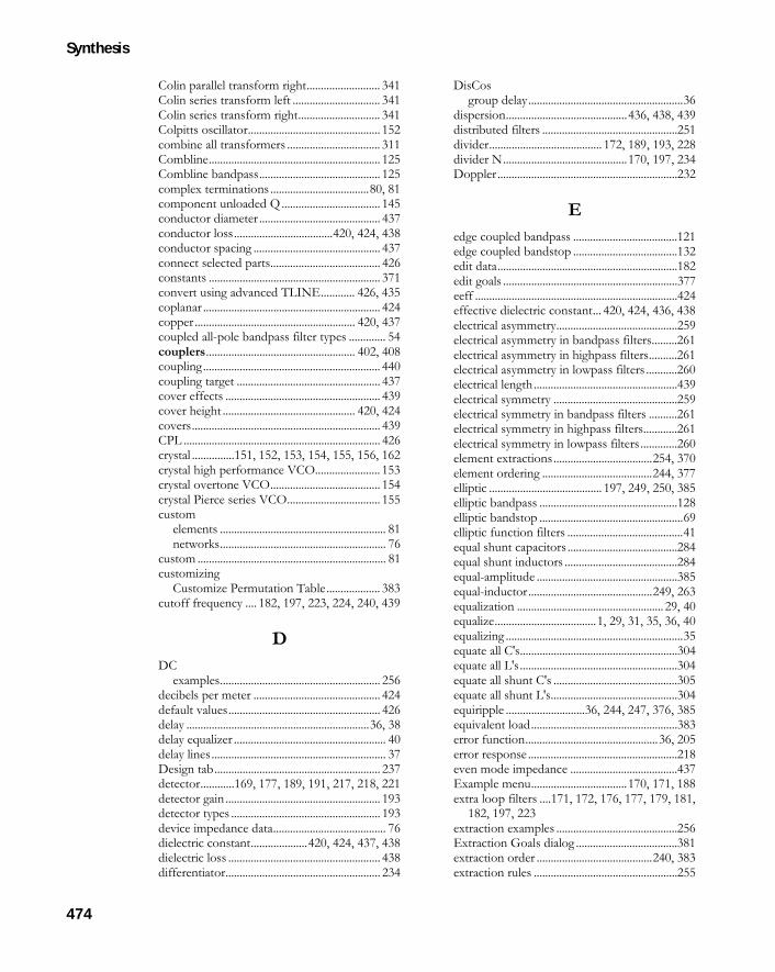
Synthesis
474
Colin parallel transform right.......................... 341 Colin series transform left ............................... 341 Colin series transform right............................. 341 Colpitts oscillator............................................... 152 combine all transformers ................................. 311 Combline............................................................. 125 Combline bandpass........................................... 125 complex terminations ...................................80, 81 component unloaded Q................................... 145 conductor diameter ........................................... 437 conductor loss...................................420, 424, 438 conductor spacing ............................................. 437 connect selected parts....................................... 426 constants ............................................................. 371 convert using advanced TLINE............ 426, 435 coplanar ............................................................... 424 copper ......................................................... 420, 437 coupled all-pole bandpass filter types ............. 54 couplers..................................................... 402, 408 coupling............................................................... 440 coupling target ................................................... 437 cover effects ....................................................... 439 cover height ............................................... 420, 424 covers................................................................... 439 CPL ...................................................................... 426 crystal ...............151, 152, 153, 154, 155, 156, 162 crystal high performance VCO....................... 153 crystal overtone VCO....................................... 154 crystal Pierce series VCO................................. 155 custom
elements ........................................................... 81 networks........................................................... 76
custom ................................................................... 81 customizing
Customize Permutation Table................... 383 cutoff frequency .... 182, 197, 223, 224, 240, 439
D DC
examples......................................................... 256 decibels per meter ............................................. 424 default values...................................................... 426 delay .................................................................36, 38 delay equalizer ...................................................... 40 delay lines.............................................................. 37 Design tab........................................................... 237 detector............169, 177, 189, 191, 217, 218, 221 detector gain ....................................................... 193 detector types ..................................................... 193 device impedance data........................................ 76 dielectric constant....................420, 424, 437, 438 dielectric loss ...................................................... 438 differentiator....................................................... 234
DisCos group delay.......................................................36
dispersion...........................................436, 438, 439 distributed filters ................................................251 divider........................................ 172, 189, 193, 228 divider N............................................170, 197, 234 Doppler................................................................232
E edge coupled bandpass .....................................121 edge coupled bandstop .....................................132 edit data................................................................182 edit goals ..............................................................377 eeff ........................................................................424 effective dielectric constant... 420, 424, 436, 438 electrical asymmetry...........................................259 electrical asymmetry in bandpass filters.........261 electrical asymmetry in highpass filters..........261 electrical asymmetry in lowpass filters ...........260 electrical length...................................................439 electrical symmetry ............................................259 electrical symmetry in bandpass filters ..........261 electrical symmetry in highpass filters............261 electrical symmetry in lowpass filters .............260 element extractions...................................254, 370 element ordering .......................................244, 377 elliptic ........................................ 197, 249, 250, 385 elliptic bandpass .................................................128 elliptic bandstop ...................................................69 elliptic function filters .........................................41 equal shunt capacitors .......................................284 equal shunt inductors ........................................284 equal-amplitude ..................................................385 equal-inductor............................................249, 263 equalization .................................................... 29, 40 equalize....................................1, 29, 31, 35, 36, 40 equalizing ...............................................................35 equate all C's........................................................304 equate all L's........................................................304 equate all shunt C's ............................................305 equate all shunt L's.............................................304 equiripple ............................36, 244, 247, 376, 385 equivalent load....................................................383 error function...............................................36, 205 error response .....................................................218 even mode impedance ......................................437 Example menu..................................170, 171, 188 extra loop filters ....171, 172, 176, 177, 179, 181,
182, 197, 223 extraction examples ...........................................256 Extraction Goals dialog ....................................381 extraction order .........................................240, 383 extraction rules ...................................................255

Index
475
extraction sequence..........................249, 255, 377 extractions..... 240, 244, 249, 251, 255, 260, 261,
370, 374, 377, 380, 381, 383 Extractions tab....... 237, 240, 244, 377, 381, 383
F features overview, S/FILTER........................ 249 FET...................................................................... 158 filter references .................................................. 469 filter synthesis......................................41, 250, 370 Filter tab .............................................172, 182, 197 filters ................................... 40, 169, 223, 224, 229 filters, user-defined............................................ 465 find dual............................................................... 303 finite frequency .................................251, 254, 374 finite zero structure extracted ......................... 374 finite zeros .... 240, 247, 255, 266, 267, 369, 374,
377, 385 Finite-Q components ......................................... 34 first example, Shape wizard ............................. 240 flicker corner ............................................. 191, 200 FM ............................................................... 232, 234 force symmetry ......................................... 280, 284 Foster's Reactance Theorem .................. 370, 371 frequencies .......................202, 214, 261, 263, 377 frequency demodulator ..........181, 189, 193, 234 frequency domain.............................182, 205, 214 frequency modulator...............177, 178, 189, 234 frequency plot control ...................................... 189 frequency sidebands.......................................... 221 frequency synthesizer..............171, 182, 189, 233 Frequency tab..................................................... 205 full transform all-pole bandstop....................... 64 full transform elliptic bandpass ........................ 66
G GIC .......................................................................... 4 GIC transform fundamentals.............................. 4 ground spacing................................................... 437 grounded L ......................................................... 293 grounded stub .................293, 294, 298, 299, 364 grounded stub, open......................................... 363 grounded, open.................................................. 360 grounded, open stub ......................................... 362 group delay..................................29, 36, 38, 39, 40
H hairpin bandpass filter ............................. 122, 426 half angle ............................................................. 272 half wavelength TLine ............................. 295, 296 harmonic ............................................................. 151
Help menu.......................................................... 188 highest accurate frequency .............................. 420 highest frequency ......................................424, 439 highpass elliptic minimum inductor .................16 highpass equalizer ................................................40 homogeneous.............................................424, 438 homogeneous coupled ..................................... 356 Hurwitz ............................................................... 370
I ideal transformer ............................................... 261 immittances ........................................................ 370 impedance function .........................254, 371, 374 impedance function Z1(s) ............................... 374 impedance matching.............................. 72, 76, 81 impedance Z(s) .................................................. 370 inductive L.......................................................... 329 inductive Pi.................................................319, 367 inductive Tee...................................................... 320 infinity........................................ 251, 255, 256, 385 inhomogeneous ................................................. 356 input parameters................................................ 437 Input tab ................................... 169, 170, 182, 187 insert element..................................................... 269 insert inverter before selected part ................ 317 instability ............................................................. 197 integrator.......................... 193, 197, 202, 207, 220 inverse Chebychev ............................................ 250 inverter ............................. 193, 315, 316, 317, 329 Inverter-TLine-Inverter ................................... 297
J JFET .................................................................... 202
K Kuroda Minnis CD left.................................... 345 Kuroda Minnis CD right ................................. 345
L Lange couplers ................................................ 411 last pole multiplier.....................................172, 197 LC......................................................................... 298 LC bandpass..........................................................79 LC bipolar........................................................... 135 L-C bipolar amplifier VCO............................. 156 LC bipolar oscillator ......................................... 158 LC Clapp............................................................. 135 L-C Clapp VCO ........................................157, 158 LC Colpitts ........................................135, 157, 158 LC hybrid............................................................ 135
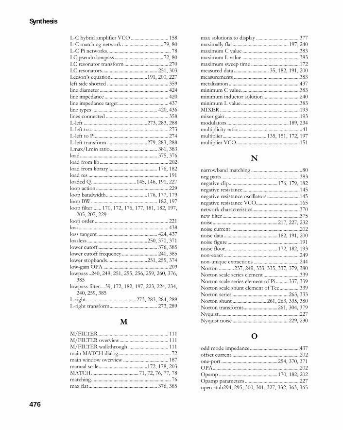
Synthesis
476
L-C hybrid amplifier VCO .............................. 158 L-C matching network .................................79, 80 L-C Pi networks................................................... 78 LC pseudo lowpass .......................................72, 80 LC resonator transform ................................... 270 LC resonators............................................ 251, 303 Leeson’s equation.............................191, 200, 227 left side shorted ................................................. 359 line diameter ....................................................... 424 line impedance ................................................... 420 line impedance target........................................ 437 line types .................................................... 420, 436 lines connected .................................................. 358 L-left ...................................................273, 283, 288 L-left to................................................................ 273 L-left to Pi........................................................... 274 L-left transform ................................279, 283, 288 Lmax/Lmin ratio...................................... 381, 383 load.............................................................. 375, 376 load from lib....................................................... 202 load from library....................................... 176, 182 load res ................................................................ 191 loaded Q....................................145, 146, 191, 227 loop action .......................................................... 229 loop bandwidth.................................176, 177, 179 loop BW ..................................................... 182, 197 loop filter....... 170, 172, 176, 177, 181, 182, 197,
205, 207, 229 loop order ........................................................... 221 loss........................................................................ 438 loss tangent ................................................ 424, 437 lossless ................................................250, 370, 371 lower cutoff ............................................... 376, 385 lower cutoff frequency ............................ 240, 385 lower stopbands................................251, 255, 374 low-gain OPA .................................................... 209 lowpass ..240, 249, 251, 255, 256, 259, 260, 376,
385 lowpass filter....39, 172, 182, 197, 223, 224, 234,
240, 259, 385 L-right........................................273, 283, 284, 289 L-right transform...................................... 273, 289
M M/FILTER ........................................................ 111 M/FILTER overview....................................... 111 M/FILTER walkthrough ................................ 111 main MATCH dialog.......................................... 72 main window overview .................................... 187 manual scale.......................................172, 178, 203 MATCH...................................... 71, 72, 76, 77, 78 matching................................................................ 76 max flat ....................................................... 376, 385
max solutions to display ...................................377 maximally flat .............................................197, 240 maximum C value ..............................................383 maximum L value ..............................................383 maximum sweep time .......................................172 measured data ............................ 35, 182, 191, 200 measurements .....................................................383 metalization .........................................................437 minimum C value...............................................383 minimum inductor solution .............................240 minimum L value ...............................................383 MIXER ................................................................193 mixer gain ............................................................193 modulators..................................................189, 234 multiplicity ratio ...................................................41 multiplier................................... 135, 151, 172, 197 multiplier VCO...................................................151
N narrowband matching .........................................80 neg parts...............................................................383 negative clip.......................................176, 179, 182 negative resistance..............................................145 negative resistance oscillators ..........................145 negative resistance VCO...................................165 network characteristics......................................370 new filter ..............................................................375 noise....................................................217, 227, 232 noise current .......................................................202 noise data ...........................................182, 191, 200 noise figure ..........................................................191 noise floor..........................................172, 182, 193 non-exact .............................................................249 non-unique extractions .....................................244 Norton ............237, 249, 333, 335, 337, 379, 380 Norton scale series element .............................339 Norton scale series element of Pi ..........337, 339 Norton scale shunt element of Tee................339 Norton series .............................................263, 333 Norton shunt ........................... 261, 263, 335, 380 Norton transforms...........................261, 304, 379 Nyquist.................................................................227 Nyquist noise .............................................229, 230
O odd mode impedance........................................437 offset current.......................................................202 one-port .............................................254, 370, 371 OPA......................................................................202 Opamp ...............................................170, 182, 202 Opamp parameters ............................................227 open stub294, 295, 300, 301, 327, 332, 363, 365
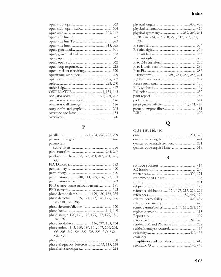
Index
477
open stub, open ................................................. 363 open stub, open stub ........................................ 364 open stubs.................................................. 305, 367 open wire line Pi ................................................ 322 open wire line Tee ............................................. 323 open wire lines .......................................... 318, 325 open, grounded.................................................. 361 open, grounded stub ......................................... 362 open, open .......................................................... 361 open, open stub ................................................. 362 open-loop response........................................... 215 open-or short-circuiting ................................... 370 operational amplifiers ....................................... 229 optimization............................................... 255, 377 order............................................................ 224, 240 order help............................................................ 467 OSCILLATOR.....................................1, 136, 143 oscillator noise ..................................191, 200, 227 oscillator type overview.................................... 146 oscillator walkthrough ...................................... 136 output tabs and graphs ..................................... 203 overtone oscillator............................................. 154 overviews ............................................................ 370
P parallel LC........................271, 294, 296, 297, 299 parameter ranges................................................ 426 parameters
active filters...................................................... 26 parts transform.......................................... 266, 267 passband ripple ..... 182, 197, 244, 247, 251, 376,
385 PD/Divider tab ................................................. 193 permeability ........................................................ 420 permittivity.......................................................... 420 permutation ............ 240, 244, 255, 256, 377, 383 permutation error .............................................. 383 PFD charge pump output current ................. 181 PFD current........................................................ 193 phase demodulator..................179, 180, 189, 235 phase detector ....... 169, 171, 172, 176, 177, 179,
180, 181, 182, 205 phase detector/divider ..................................... 170 phase lock................................................... 148, 149 phase margin 170, 171, 172, 176, 177, 179, 181,
182, 197 phase modulator ......................176, 177, 189, 234 phase noise.... 143, 169, 189, 191, 197, 200, 202,
203, 205, 217, 224, 227, 228, 229, 230, 232, 234, 235
phase shift ............................................................. 38 phase/frequency detectors .............193, 219, 228 phaselock techniques ........................................ 214
physical length ...........................................420, 439 physical schematic............................................. 426 physical symmetry ............................259, 260, 261 PI 78, 274, 284, 287, 288, 291, 317, 333, 337,
339 Pi series left ........................................................ 354 Pi series right...................................................... 354 Pi shunt left ........................................................ 354 Pi shunt right...................................................... 355 Pi to 2-Pi transform.......................................... 286 Pi to L-Left transform...................................... 283 Pi to Pi................................................................. 286 Pi transform .................... 280, 284, 286, 287, 291 Pi/Tee transforms............................................. 237 Pierce oscillator.................................................. 155 PLL synthesis ..................................................... 169 PM noise ............................................................. 232 print report ......................................................... 188 probability........................................................... 374 propagation velocity ........................420, 424, 439 pseudo lowpass filter ...........................................81 PSRR.................................................................... 202
Q Q 34, 145, 146, 440 quad..............................................................271, 370 quarter wavelength............................................ 424 quarter wavelength frequency......................... 251 quarter wavelength TLine................................ 319
R rat race splitters............................................... 414 RC bandwidth.................................................... 200 reactances....................................................370, 371 recommended ranges ....................................... 426 reentry.................................................................. 251 ref period ............................................................ 193 reference sidebands........ 171, 197, 215, 221, 224 references...........................................189, 469, 470 relative permeability..................................420, 437 relative permittivity ........................................... 420 remove transformer ................ 249, 260, 261, 379 replace element .................................................. 315 Report tab........................................................... 207 rescale plot..................................................240, 376 residual FM and PM noise .............................. 232 residuals analysis control.................................. 189 resistivity .....................................................437, 438 resistors
splitters and couplers............................... 416 resonator Q ................................................146, 440

Synthesis
478
resonators...... 227, 244, 251, 254, 261, 263, 266, 267, 333, 335, 374, 377, 383, 440
Rho....................................................................... 423 right side shorted............................................... 358 ripple .................................................................... 376 Rload.................................................................... 310 roughness ............................................................ 420 Rsource................................................................ 309
S S/FILTER Extraction Goals dialog..... 377, 381 S/FILTER schematic .............................. 240, 379 S/FILTER specifications ................................ 240 S/FILTER Specifications tab ......................... 376 S/FILTER Start tab.......................................... 375 S/FILTER window .......................................... 237 sampling rate ...................................................... 189 save settings............................................... 375, 376 save to library ..................................................... 202 SAW............................................................ 156, 162 SAW oscillators.................................162, 163, 164 scale inverter....................................................... 315 scale selected element ....................................... 316 scale series element of Pi ................................. 337 scale source......................................................... 316 scaled down TLine ............................................ 368 scaled up TLine and stubs ............................... 368 section types ......................................................... 31 sensitivity............................................................. 214 series....................................................251, 379, 383 series C ......................................312, 313, 314, 324 series element first...................240, 244, 256, 377 series half wavelenth TLine............................. 301 series inductor ...................................251, 371, 374 series L.............293, 299, 311, 312, 313, 314, 323 series LC....................................251, 295, 296, 301 series open left ................................................... 342 series open right................................................. 343 series res .............................................................. 383 series shorted left............................................... 342 series shorted right ............................................ 342 series transmission lines ................................... 251 Shape wizard ............................................. 375, 376 shift left ............................................................... 305 shift leftmost ...................................................... 306 shift right............................................................. 307 shift rightmost.................................................... 308 shorted stub............................................... 327, 332 shorted stubs ............................................. 304, 318 shorted wire............................................... 322, 364 shorted wire line ................................................ 324 shorted wire line Pi ........................................... 321 show in table ...................................................... 383
shunt C............294, 300, 312, 313, 314, 326, 369 shunt C coupled bandpass filter........................58 shunt first.............................................................377 shunt grounded left ...........................................343 shunt grounded right.........................................343 shunt L ............................. 311, 312, 313, 314, 325 shunt open left....................................................344 shunt open right .................................................344 shunt res...............................................................383 shunt shorted left ...............................................350 shunt shorted right.............................................350 shunt-C coupled bandpass filter ................ 40, 41 Sim tab ........................................................189, 203 simplify.....................266, 267, 333, 335, 379, 380 simplify circuit ....................................................379 single-sideband ...................................................227 skin depth ............................................................438 Smith Chart based matching programs ...........71 solution table...........240, 244, 249, 377, 381, 383 sources....................................................................76 specifications...........237, 240, 244, 247, 376, 385 Specifications tab ..237, 240, 244, 247, 251, 376,
385 specify left............................................................333 specify right .........................................................333 specify transformer ratio (N) ...........................333 split element transform...................263, 266, 267 splitters
backward wave............................................402 branch line....................................................408
Sr 423, 437 SSB...............................................................189, 191 stability .......................76, 170, 205, 229, 230, 234 start S/FILTER..................................................240 Start tab................................................................375 starting TLINE...................................................419 Status button.......................................................170 step stub......................................................369, 370 stepped impedance transmission line filter .....81 stopband attenuation................................251, 385 striplines...............................................................439 stub highpass.......................................................131 stub lowpass ........................................................130 stub Tee ...............................................................367 stub/open wire line ...........................................296 stub/shorted wire line.......................................297 stubs.................................. 321, 322, 323, 366, 368 substrate thickness .............................................424 substrates
Advanced TLINE example ........................426 Summary tab .........................................................78 supported Pi element ........................................284 surface roughness.............................420, 437, 438 swap element with one to right transform....269 switching time 172, 176, 179, 180, 181, 182, 189
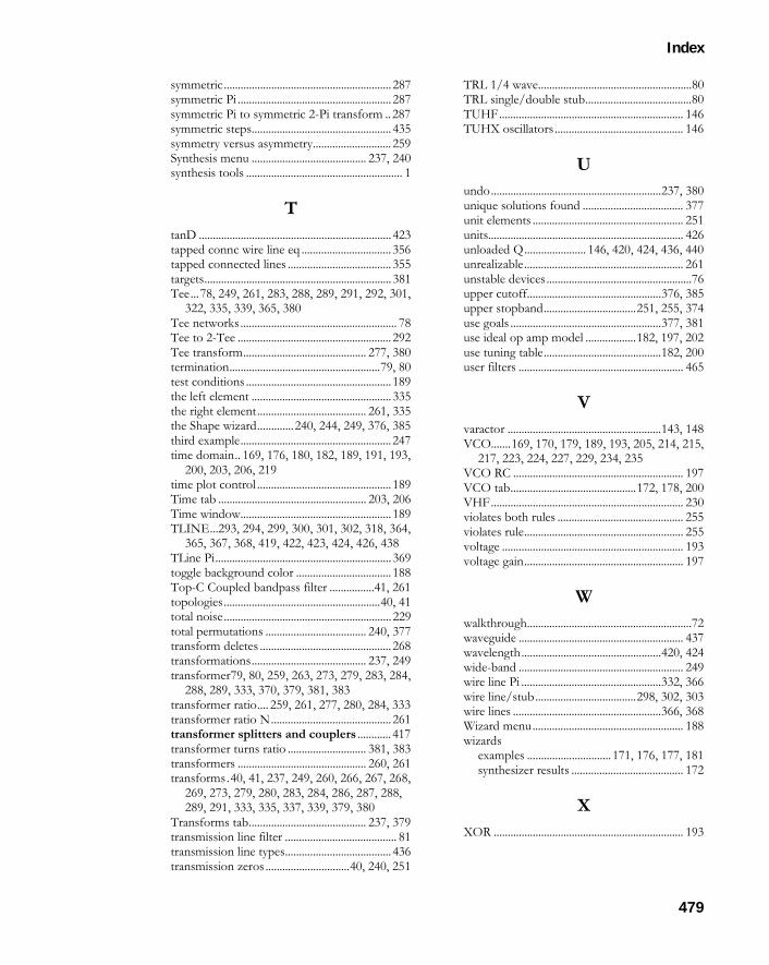
Index
479
symmetric............................................................ 287 symmetric Pi ....................................................... 287 symmetric Pi to symmetric 2-Pi transform ..287 symmetric steps.................................................. 435 symmetry versus asymmetry............................ 259 Synthesis menu ......................................... 237, 240 synthesis tools ........................................................ 1
T tanD ..................................................................... 423 tapped connc wire line eq ................................ 356 tapped connected lines ..................................... 355 targets................................................................... 381 Tee...78, 249, 261, 283, 288, 289, 291, 292, 301,
322, 335, 339, 365, 380 Tee networks ........................................................ 78 Tee to 2-Tee ....................................................... 292 Tee transform............................................ 277, 380 termination......................................................79, 80 test conditions .................................................... 189 the left element .................................................. 335 the right element....................................... 261, 335 the Shape wizard.............240, 244, 249, 376, 385 third example...................................................... 247 time domain.. 169, 176, 180, 182, 189, 191, 193,
200, 203, 206, 219 time plot control ................................................ 189 Time tab ..................................................... 203, 206 Time window...................................................... 189 TLINE...293, 294, 299, 300, 301, 302, 318, 364,
365, 367, 368, 419, 422, 423, 424, 426, 438 TLine Pi............................................................... 369 toggle background color .................................. 188 Top-C Coupled bandpass filter ................41, 261 topologies........................................................40, 41 total noise............................................................ 229 total permutations .................................... 240, 377 transform deletes ............................................... 268 transformations......................................... 237, 249 transformer79, 80, 259, 263, 273, 279, 283, 284,
288, 289, 333, 370, 379, 381, 383 transformer ratio.... 259, 261, 277, 280, 284, 333 transformer ratio N........................................... 261 transformer splitters and couplers ............ 417 transformer turns ratio ............................ 381, 383 transformers .............................................. 260, 261 transforms.40, 41, 237, 249, 260, 266, 267, 268,
269, 273, 279, 280, 283, 284, 286, 287, 288, 289, 291, 333, 335, 337, 339, 379, 380
Transforms tab.......................................... 237, 379 transmission line filter ........................................ 81 transmission line types...................................... 436 transmission zeros ..............................40, 240, 251
TRL 1/4 wave.......................................................80 TRL single/double stub......................................80 TUHF.................................................................. 146 TUHX oscillators .............................................. 146
U undo.............................................................237, 380 unique solutions found .................................... 377 unit elements ...................................................... 251 units...................................................................... 426 unloaded Q...................... 146, 420, 424, 436, 440 unrealizable......................................................... 261 unstable devices....................................................76 upper cutoff................................................376, 385 upper stopband.................................251, 255, 374 use goals ......................................................377, 381 use ideal op amp model ..................182, 197, 202 use tuning table..........................................182, 200 user filters ........................................................... 465
V varactor .......................................................143, 148 VCO.......169, 170, 179, 189, 193, 205, 214, 215,
217, 223, 224, 227, 229, 234, 235 VCO RC ............................................................. 197 VCO tab.............................................172, 178, 200 VHF..................................................................... 230 violates both rules ............................................. 255 violates rule......................................................... 255 voltage ................................................................. 193 voltage gain......................................................... 197
W walkthrough...........................................................72 waveguide ........................................................... 437 wavelength..................................................420, 424 wide-band ........................................................... 249 wire line Pi ..................................................332, 366 wire line/stub....................................298, 302, 303 wire lines .....................................................366, 368 Wizard menu...................................................... 188 wizards
examples .............................. 171, 176, 177, 181 synthesizer results ........................................ 172
X XOR .................................................................... 193

Synthesis
480
Y yield ............................................................. 377, 385
Z zero table .................................. 240, 244, 376, 385 Zoe........................................................................437 Zoo impedance...................................................437


![[ICdesignVN.com]--verilog coding for logic synthesis.pdf](https://img.pdfslide.net/doc/110x75/55cf9b1a550346d033a4bb59/icdesignvncom-verilog-coding-for-logic-synthesispdf.jpg)