Embed Size (px)
Citation preview
A M S D E S I G N & V E R I F I C A T I O N WH
IT
EP
AP
ER
w w w . m e n t o r . c o m
SYSTEM-LEVEL MEMS DESIGN - EXPLORING MODELING AND SIMULATION METHODOLOGIES
QI JING, TECHNICAL MARKETING ENGINEER, MENTOR GRAPHICS
w w w. m ento r.co m2
System-Level MEMS Design - Exploring Modeling and Simulation Methodologies
INTRODUCTIONBeginning in the 1980’s with the first rotary electrostatic side drive motor brought to the world at UC Berkley, and followed in the 1990’s with the first surface-micromachined accelerometer manufactured in volume by Analog Devices, MicroElectroMechanical Systems (MEMS) have been steadily evolving from pure research into an emerging industry that is gaining more and more attention and investment. Today, MEMS devices not only have moved into mass production for applications such as inertial measurement units and acoustic sensors, but also have expanded into broader scopes such as optical MEMS, microfluidics, and bio-MEMS.
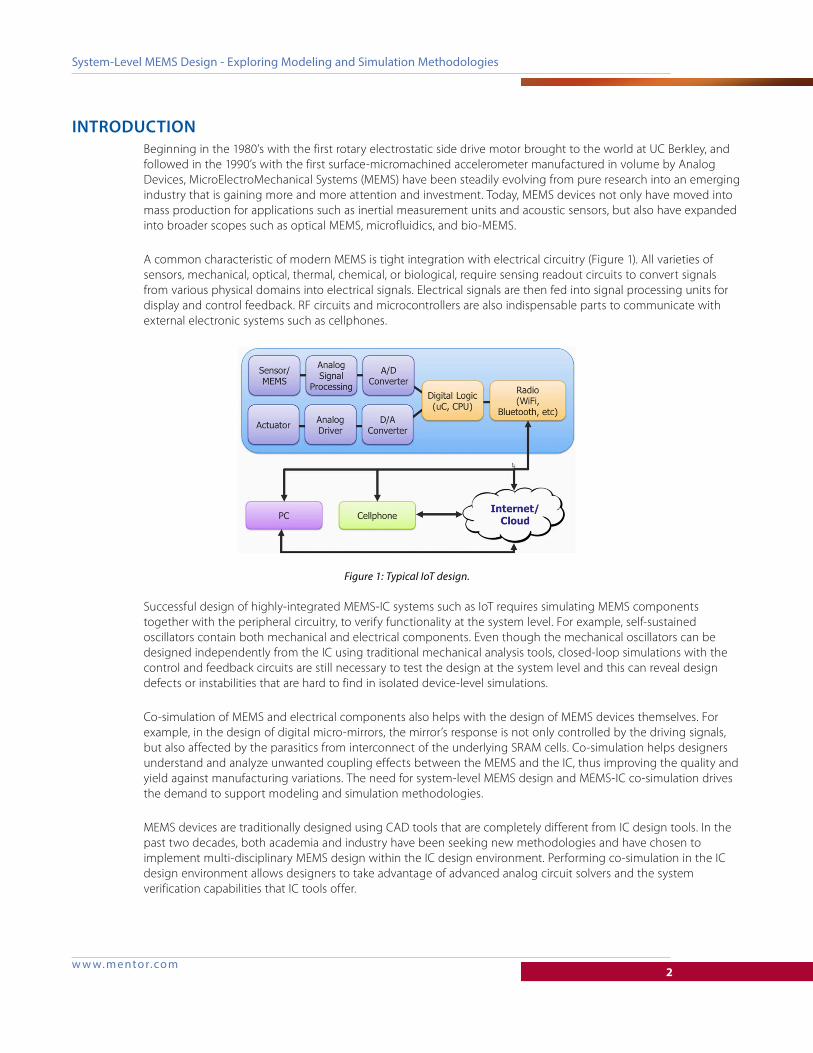
A common characteristic of modern MEMS is tight integration with electrical circuitry (Figure 1). All varieties of sensors, mechanical, optical, thermal, chemical, or biological, require sensing readout circuits to convert signals from various physical domains into electrical signals. Electrical signals are then fed into signal processing units for display and control feedback. RF circuits and microcontrollers are also indispensable parts to communicate with external electronic systems such as cellphones.
Figure 1: Typical IoT design.
Successful design of highly-integrated MEMS-IC systems such as IoT requires simulating MEMS components together with the peripheral circuitry, to verify functionality at the system level. For example, self-sustained oscillators contain both mechanical and electrical components. Even though the mechanical oscillators can be designed independently from the IC using traditional mechanical analysis tools, closed-loop simulations with the control and feedback circuits are still necessary to test the design at the system level and this can reveal design defects or instabilities that are hard to find in isolated device-level simulations.
Co-simulation of MEMS and electrical components also helps with the design of MEMS devices themselves. For example, in the design of digital micro-mirrors, the mirror’s response is not only controlled by the driving signals, but also affected by the parasitics from interconnect of the underlying SRAM cells. Co-simulation helps designers understand and analyze unwanted coupling effects between the MEMS and the IC, thus improving the quality and yield against manufacturing variations. The need for system-level MEMS design and MEMS-IC co-simulation drives the demand to support modeling and simulation methodologies.
MEMS devices are traditionally designed using CAD tools that are completely different from IC design tools. In the past two decades, both academia and industry have been seeking new methodologies and have chosen to implement multi-disciplinary MEMS design within the IC design environment. Performing co-simulation in the IC design environment allows designers to take advantage of advanced analog circuit solvers and the system verification capabilities that IC tools offer.
w w w. m ento r.co m3
System-Level MEMS Design - Exploring Modeling and Simulation Methodologies
A good system-level design methodology should facilitate MEMS device models and structure representations that are compatible with the IC design flow, and provide simulation accuracy and speed that are comparable or superior to typical analysis tools in the appropriate physical domains. It should also provide broad coverage of physical effects, and be able to support large system complexity as well as quick design iteration.
FUNDAMENTALS OF SYSTEM-LEVEL MODELING AND MEMS-IC CO-SIMULATION
Today’s IC design tools are based on SPICE models and simulators, which despite the large variety of tool implementations, share the following common characteristics:
• Device models are lumped, parameterized behavioral models
• Circuits and systems are described in a structural and hierarchical format
Although circuit designers tend to think of transistors as the smallest, lowest-level constitutional element of electrical circuits, each transistor is actually a distributed physical system. Based on semiconductor device physics, classical SPICE models, such as Berkeley Short-channel IGFET Models (BSIM) models, intelligently concentrate or lump the distributed physical behavior happening inside and around a CMOS transistor into four terminals: Drain (D), Gate (G), Source (S), and Bulk (B), with each terminal having an associated pair of across variable (voltage, V) and through variable (current, I). Device behavior is then described using a set of algebraic differential equations, plus the specification of process and device parameters, to form the relationships between V and I of the pertinent terminals.
Parameterization permits designers to use circuit devices as general building blocks (instances) for system composition, and the device terminals serve as channels for interconnection and energy exchange with other devices. By instantiating and wiring up individual devices, the designer forms the network (circuit topology). Applying this same method to higher-level blocks, large systems are built up structurally and hierarchically. SPICE simulators then stamp each individual device into system matrices and form simultaneous equations based on circuit topologies, Kirchhoff’s Voltage Law (KVL) and Kirchhoff’s Current Law (KCL), to solve for a self-consistent solution for the whole system.
SPICE models and simulators are usually integrated into a schematic capture environment, to provide a graphical interface for design entry and editing. Each cell in a design has a symbol view for schematic capture and a model view for simulation. The cell can also have a layout view for physical implementation, and other views such as the parasitic-extracted view for more advanced design needs, together forming a complete IC design representation.
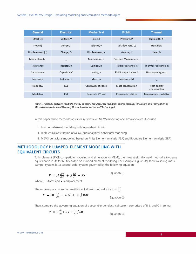
A successful MEMS modeling and simulation methodology should be compatible and interoperable with the IC design environment described above, in order to enable system-level design and MEMS-IC co-simulation. The feasibility of this methodology depends on the analogy between multiple energy domains. Table 1 shows the effort (across variable) and flow (through variable) of the electrical domain and the counterparts in mechanical, fluidic and thermal domains. Similar analogies exist for other physical domains not shown in the table, such as the optical and magnetic domains.
w w w. m ento r.co m4
System-Level MEMS Design - Exploring Modeling and Simulation Methodologies
Table 1: Analogy between multiple energy domains (Source: Joel Voldman, course material for Design and Fabrication of Microelectromechanical Devices, Massachusetts Institute of Technology).
In this paper, three methodologies for system-level MEMS modeling and simulation are discussed:
I. Lumped-element modeling with equivalent circuits
II. Hierarchical abstraction of MEMS and analytical behavioral modeling
III. MEMS behavioral modeling based on Finite Element Analysis (FEA) and Boundary Element Analysis (BEA)
METHODOLOGY I: LUMPED-ELEMENT MODELING WITH EQUIVALENT CIRCUITS
To implement SPICE-compatible modeling and simulation for MEMS, the most straightforward method is to create equivalent circuits for MEMS based on lumped-element modeling. For example, Figure 2(a) shows a spring-mass-damper system. It’s a second-order system governed by the following equation:
Equation (1)
Where F is force and x is displacement.
The same equation can be rewritten as follows using velocity :
Equation (2)
Then, compare the governing equation of a second-order electrical system comprised of R, L, and C in series:
Equation (3)
w w w. m ento r.co m5
System-Level MEMS Design - Exploring Modeling and Simulation Methodologies
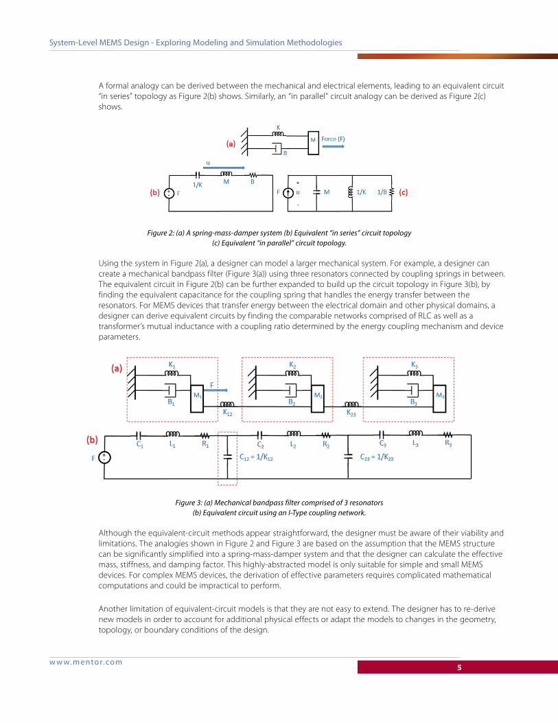
A formal analogy can be derived between the mechanical and electrical elements, leading to an equivalent circuit “in series” topology as Figure 2(b) shows. Similarly, an “in parallel” circuit analogy can be derived as Figure 2(c) shows.
Figure 2: (a) A spring-mass-damper system (b) Equivalent “in series” circuit topology (c) Equivalent “in parallel” circuit topology.
Using the system in Figure 2(a), a designer can model a larger mechanical system. For example, a designer can create a mechanical bandpass filter (Figure 3(a)) using three resonators connected by coupling springs in between. The equivalent circuit in Figure 2(b) can be further expanded to build up the circuit topology in Figure 3(b), by finding the equivalent capacitance for the coupling spring that handles the energy transfer between the resonators. For MEMS devices that transfer energy between the electrical domain and other physical domains, a designer can derive equivalent circuits by finding the comparable networks comprised of RLC as well as a transformer’s mutual inductance with a coupling ratio determined by the energy coupling mechanism and device parameters.
Figure 3: (a) Mechanical bandpass filter comprised of 3 resonators (b) Equivalent circuit using an I-Type coupling network.
Although the equivalent-circuit methods appear straightforward, the designer must be aware of their viability and limitations. The analogies shown in Figure 2 and Figure 3 are based on the assumption that the MEMS structure can be significantly simplified into a spring-mass-damper system and that the designer can calculate the effective mass, stiffness, and damping factor. This highly-abstracted model is only suitable for simple and small MEMS devices. For complex MEMS devices, the derivation of effective parameters requires complicated mathematical computations and could be impractical to perform.
Another limitation of equivalent-circuit models is that they are not easy to extend. The designer has to re-derive new models in order to account for additional physical effects or adapt the models to changes in the geometry, topology, or boundary conditions of the design.
w w w. m ento r.co m6
System-Level MEMS Design - Exploring Modeling and Simulation Methodologies
Due to these limitations, it is not uncommon for designers to determine that equivalent-circuit methods are too difficult or impossible to implement. Therefore, they need a more advanced methodology that supports MEMS modeling in a more accurate and practical way. By taking advantage of the support of analog hardware description languages in SPICE simulators, more powerful MEMS modeling approaches are possible for MEMS-IC co-simulation at the system level.
METHODOLOGY II: HIERARCHICAL ABSTRACTION OF MEMS AND ANALYTICAL BEHAVIORAL MODELING
The next methodology focuses on hierarchical abstraction of MEMS and the use of analytical behavioral models for system-level design and verification.
In IC design, complex systems are built up hierarchically using building blocks at different abstraction levels. Starting from fundamental elements such as transistors and RLCs, the designer builds functional blocks, like operational amplifiers, that are then used as building blocks for higher level blocks and systems. The designer represents the whole system by using hierarchical schematics that define a structural network comprising instances of these building blocks, connected together based on a designed topology.
This methodology is flexible, reusable and scalable, and is powerful for IC design. Similar ideas have been explored and applied to MEMS design and have been proven feasible, yet challenging, because of the uniqueness and variety of MEMS devices.
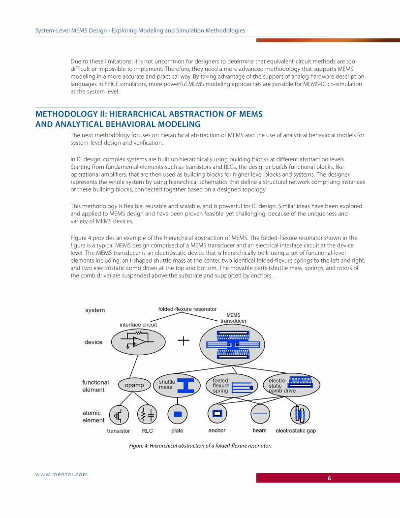
Figure 4 provides an example of the hierarchical abstraction of MEMS. The folded-flexure resonator shown in the figure is a typical MEMS design comprised of a MEMS transducer and an electrical interface circuit at the device level. The MEMS transducer is an electrostatic device that is hierarchically built using a set of functional-level elements including: an I-shaped shuttle mass at the center, two identical folded-flexure springs to the left and right, and two electrostatic comb drives at the top and bottom. The movable parts (shuttle mass, springs, and rotors of the comb drive) are suspended above the substrate and supported by anchors.
Figure 4: Hierarchical abstraction of a folded-flexure resonator.
w w w. m ento r.co m7
System-Level MEMS Design - Exploring Modeling and Simulation Methodologies
The folded-flexure spring and the electrostatic comb drive are two different functional-level elements that each have their own structural topologies and working principals. However, they share some common characteristics:
• The folded-flexure spring can be further decomposed into anchors plus a group of beams of different sizes and orientations.
• The comb drive can be further decomposed into interconnected anchors and beams as well, plus electrostatic gaps to model the mechanical and electrostatic coupling between stator and rotor comb fingers. This is because the actual comb fingers are not ideal rigid bodies and they behave like beams when the bending effect is non-negligible.
As shown in Figure 4, functional-level elements of the resonator can be further decomposed into atomic-level elements including plates, anchors, beams, and electrostatic gaps.
This group of atomic-level elements not only serves as foundational building blocks for the folded-flexure resonator, but also provide building blocks for many other typical suspended MEMS designs, such as accelerometers, gyroscopes, resonator filters, micro mirrors, and RF switches. These elements form a useful model library for the suspended MEMS design space.
MEMS modeling can also be done at mixed levels of abstraction. For example, when the comb fingers have high stiffness, they can be modeled directly at the functional level as a rigid-body element, without being decomposed into beams and electrostatic gaps. Model accuracy will degrade slightly, and the high-level comb drive can still be connected to lower-level models such as the plates for simulation.
The designer can write behavioral models for MEMS using analog hardware description languages such as Verilog-A, Verilog-AMS, or VHDL-AMS. These languages define constructs that are specially-designed for multi-disciplinary modeling. Most of today’s SPICE simulators support Verilog-A, because of the need for compact modeling of electronic devices. Therefore, Verilog-A models for MEMS are intrinsically compatible with SPICE simulators and are a good choice for supporting co-simulation with electronic circuits within the IC design environment.
Analytical behavioral models for MEMS should contain the following elements, which are similar to those for compact modeling of ICs:
• The definition of terminals (also called nodes), with the associated physical discipline specified.
• The definition of model parameters, including material and process properties as well as geometric sizing and orientation parameters.
• The description of model behavior using a series of Differential Algebraic Equations (DAEs) that govern the relationship between across and through variables of the terminals, with coefficients formed by parameters and internal variables.
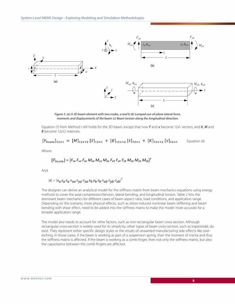
Figure 5 shows how a 3D beam model in the atomic-element model library illustrated in Figure 4 is formed. The beam behavior is lumped into two terminals, node a and node b, as shown in Figure 5(a). The x-direction represents the longitudinal direction. Depending on the direction and type of load, the beam could have linear axial compression/tension, in-plane lateral bending, out-of-plane lateral bending (Figure 5b), as well as torsion along the longitudinal direction (Figure 5c). Therefore, the beam can have lateral displacements along the x, y and z-axis respectively and rotations around the x, y and z-axis as well, at both node a and node b.
Adding all these motions together means that the beam is a 12-DOF (Degree of Freedom) element, which is much more complex than the highly-simplified 1-DOF lumped-element model presented in Method I, Figure 2.
w w w. m ento r.co m8
System-Level MEMS Design - Exploring Modeling and Simulation Methodologies
Figure 5: (a) A 3D beam element with two nodes, a and b (b) Lumped out-of-plane lateral force, moments and displacements of the beam (c) Beam torsion along the longitudinal direction.
Equation (1) from Method I still holds for the 3D beam, except that now F and x become 12x1 vectors, and K, M and B become 12x12 matrices:
Equation (4)
Where:
And:
[x] = [xa ya za øxa øya øza xb yb zb øxb øyb øzb]T
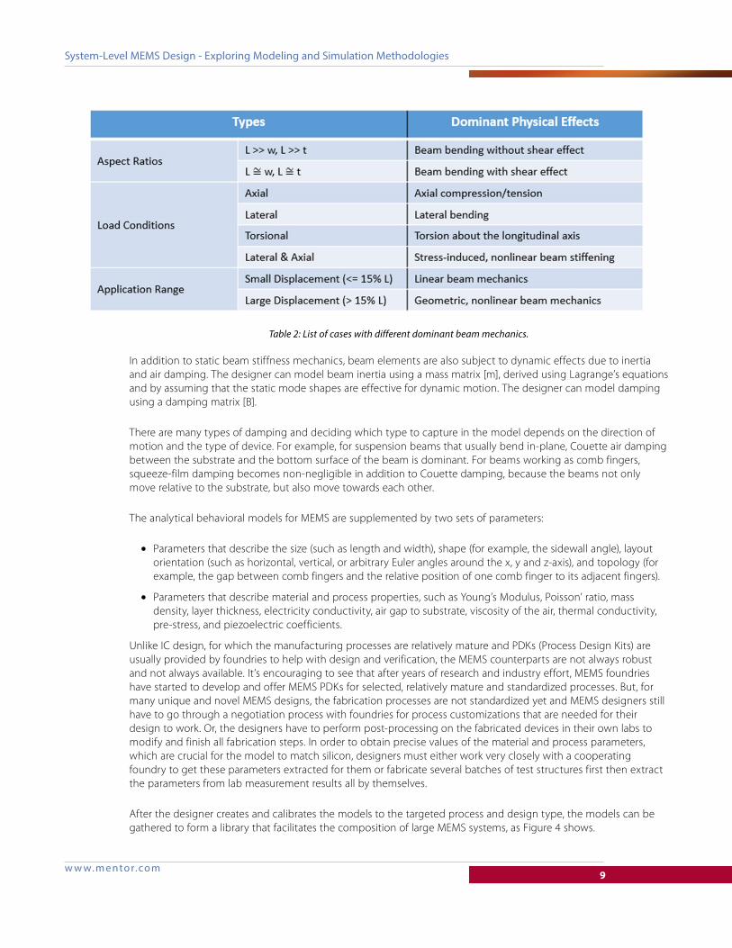
The designer can derive an analytical model for the stiffness matrix from beam mechanics equations using energy methods to cover the axial compression/tension, lateral bending, and longitudinal torsion. Table 2 lists the dominant beam mechanics for different cases of beam aspect ratio, load conditions, and application range. Depending on the scenario, more physical effects, such as stress-induced nonlinear beam stiffening and beam bending with shear effect, need to be added into the stiffness matrix to make the model more accurate for a broader application range.
The model also needs to account for other factors, such as non-rectangular beam cross-section. Although rectangular cross-section is widely-used for its simplicity, other types of beam cross-section, such as trapezoidal, do exist. They represent either specific design styles or the results of unwanted manufacturing side-effects like over-etching. In those cases, if the beam is working as part of a suspension spring, then the moment of inertia and thus the stiffness matrix is affected. If the beam is working as a comb finger, then not only the stiffness matrix, but also the capacitance between the comb fingers are affected.
w w w. m ento r.co m9
System-Level MEMS Design - Exploring Modeling and Simulation Methodologies
Table 2: List of cases with different dominant beam mechanics.
In addition to static beam stiffness mechanics, beam elements are also subject to dynamic effects due to inertia and air damping. The designer can model beam inertia using a mass matrix [m], derived using Lagrange’s equations and by assuming that the static mode shapes are effective for dynamic motion. The designer can model damping using a damping matrix [B].
There are many types of damping and deciding which type to capture in the model depends on the direction of motion and the type of device. For example, for suspension beams that usually bend in-plane, Couette air damping between the substrate and the bottom surface of the beam is dominant. For beams working as comb fingers, squeeze-film damping becomes non-negligible in addition to Couette damping, because the beams not only move relative to the substrate, but also move towards each other.
The analytical behavioral models for MEMS are supplemented by two sets of parameters:
• Parameters that describe the size (such as length and width), shape (for example, the sidewall angle), layout orientation (such as horizontal, vertical, or arbitrary Euler angles around the x, y and z-axis), and topology (for example, the gap between comb fingers and the relative position of one comb finger to its adjacent fingers).
• Parameters that describe material and process properties, such as Young’s Modulus, Poisson’ ratio, mass density, layer thickness, electricity conductivity, air gap to substrate, viscosity of the air, thermal conductivity, pre-stress, and piezoelectric coefficients.
Unlike IC design, for which the manufacturing processes are relatively mature and PDKs (Process Design Kits) are usually provided by foundries to help with design and verification, the MEMS counterparts are not always robust and not always available. It’s encouraging to see that after years of research and industry effort, MEMS foundries have started to develop and offer MEMS PDKs for selected, relatively mature and standardized processes. But, for many unique and novel MEMS designs, the fabrication processes are not standardized yet and MEMS designers still have to go through a negotiation process with foundries for process customizations that are needed for their design to work. Or, the designers have to perform post-processing on the fabricated devices in their own labs to modify and finish all fabrication steps. In order to obtain precise values of the material and process parameters, which are crucial for the model to match silicon, designers must either work very closely with a cooperating foundry to get these parameters extracted for them or fabricate several batches of test structures first then extract the parameters from lab measurement results all by themselves.
After the designer creates and calibrates the models to the targeted process and design type, the models can be gathered to form a library that facilitates the composition of large MEMS systems, as Figure 4 shows.
w w w. m ento r.co m10
System-Level MEMS Design - Exploring Modeling and Simulation Methodologies
Creation of a good analytical model for MEMS requires significant effort and a deep understanding of the process, design, and the underlying physics. However, after the models are developed, using them is a straightforward process. Accompanied by the symbol view, the designer can directly instantiate MEMS elements into a schematic and connect them to other MEMS elements and electrical elements such as transistors and RLCs, to build up a complex MEMS system for co-simulation.
A MEMS behavioral model library makes it possible for people who might not have expertise in MEMS, such as electrical circuit designers or system integration engineers, to use and simulate the MEMS components as black boxes. The model library also helps protect details of the IP implementation. MEMS component vendors can ship calibrated behavioral models of their devices to customers without revealing sensitive information about their design and fabrication process.
For successful adoption and prevalence of the analytical modeling methodology, coverage of physical effects and design types is the key. Currently, relatively mature MEMS designs, such as inertial sensors, microphones, and RF MEMS, have progressed into mass production. The associated processes have become more and more reliable and standardized. This makes developing behavioral model libraries possible and helps them be adopted by the industry. Today, powerful component libraries are available that include beams and suspension springs of different geometries, rigid and flexible plates, and comb drives with rigid or flexible fingers (with or without fringing field and damping). Model library development is also progressing well in other fields such as piezoelectric and optical.
However, due to the large variety and broad variations of MEMS designs and the associated underlying physics, fabrication processes, and design styles, no model library can be a universal solution that fits all design situations. If the device employs unique, irregular geometries, or if the device involves physics mechanisms that are not well-understood, the existing model must undergo major modification and enhancement to meet design specifications. Or, the available model might be completely non-applicable and a new model has to be developed from scratch.
Decomposability is another factor affecting the feasibility of this methodology. Not every MEMS device and system can be decomposed in the way Figure 4 presents. For new fields of study, such as bio-MEMS and microfluidics, processes and design styles are still being explored through trial-and-error experiments. Whether a group of representative elements exists or not is still unclear, and the supply and demand of models for these fields of study are still at an early stage.
METHODOLOGY III: MEMS BEHAVIORAL MODELING BASED ON FEA/BEA
Because geometry shapes supported by analytical models are discrete and limited, MEMS designers sometimes resort to Finite Element Analysis (FEA) and Boundary Element Analysis (BEA) tools.
FEA/BEA tools use conventional numerical analysis methods for simulations in the mechanical, electrostatic, magnetic, and thermal domains. They often rely on auto-meshers to partition a continuum structure into a mesh comprised of low-order finite elements. The tools construct system matrices based on the meshing and solve the matrices within boundary conditions. With sufficient refinement of the meshing, the designer can obtain accurate simulation results. Various types of meshing, such as Triangular and Tetrahedra meshes, allow the designer to model arbitrary shapes. Therefore, FEA/BEA is a good complement to analytical modeling.
Efficient simulation of coupled physical domains is often a challenge to FEA/BEA-based tools. For example, to model the interaction between mechanical and electrostatic domains, which is crucial for devices such as electrostatic comb drives, some FEA/BEA tools must perform mechanical and electrostatic analyses separately and iteratively until a self-consistent, converged solution is found. Superior tools can simulate coupled domains all-together, but the simulation is computationally expensive, sometimes resulting in unacceptable run times.
w w w. m ento r.co m11
System-Level MEMS Design - Exploring Modeling and Simulation Methodologies
Moreover, since FEA/BEA is based on a 3D mesh of the continuum structure, sometimes when there are changes to the layout or the process, a new mesh must be created and the previous model cannot be reused.
To alleviate the limitations of FEA/BEA based methods, while still utilizing their strength, Reduced Order Modeling (ROM) has recently been deployed, effectively bridging the gap between traditional FEA/BEA tools and modern electrical circuit simulators.
ROM is a numerical methodology that attempts to reduce the DOF of system matrices to create macro models for MEMS devices. There are many approaches for ROM, such as Krylov-subspace-based methods, Trajectory piecewise-linear (TPWL), and higher-order Model Order Reduction (MOR). The reduced-order models can be derived based on static analysis, eigenmode analysis, or a combination of both. A common approach for linear mechanics is modal superposition. Here, the idea is to represent the mechanical deformation by a superposition of selected ‘dominant’ mode shapes. Usually, the static and dynamic behavior of a mechanical structure is sufficiently captured by a few ‘master’ eigenmodes. Contribution from eigenmodes of higher orders is limited since MEMS devices often operate in, or close to resonance. By reducing the number of eigenmodes included in the model, DOFs of the resulting matrices could decrease from thousands into tens, greatly simplifying the model and expediting the simulation, while still retaining acceptable accuracy.
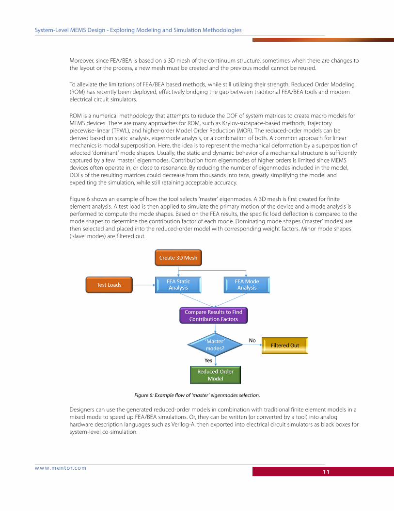
Figure 6 shows an example of how the tool selects ‘master’ eigenmodes. A 3D mesh is first created for finite element analysis. A test load is then applied to simulate the primary motion of the device and a mode analysis is performed to compute the mode shapes. Based on the FEA results, the specific load deflection is compared to the mode shapes to determine the contribution factor of each mode. Dominating mode shapes (‘master’ modes) are then selected and placed into the reduced-order model with corresponding weight factors. Minor mode shapes (‘slave’ modes) are filtered out.
Figure 6: Example flow of ‘master’ eigenmodes selection.
Designers can use the generated reduced-order models in combination with traditional finite element models in a mixed mode to speed up FEA/BEA simulations. Or, they can be written (or converted by a tool) into analog hardware description languages such as Verilog-A, then exported into electrical circuit simulators as black boxes for system-level co-simulation.
w w w. m ento r.co m12
System-Level MEMS Design - Exploring Modeling and Simulation Methodologies
In recent years, reduced-order modeling methodologies have been expanded to allow a reduced-order model to be built not only from FEA/BEA results, but also from user-defined analytical equations, experimental data, or combinations of these sources. For example, in addition to using selected mode shapes to reduce DOFs of system matrices, the designer can incorporate into the model analytical forms derived from energy methods to achieve faster calculation of nonlinear force. These advancements further enhance the efficiency and coverage of model libraries based on FEA/BEA and ROM.
Progress has also been made on the ability to preserve parameters in the reduced models, so that design variations can be evaluated without going through the FEA and the model order reduction process again, provided that the variation is within the applicable range of the original model. For major changes, such as structure shape change or topology change, the reduced-order model still must be re-generated.
Like all modeling methodologies, FEA/BEA-based methods cannot fully cover the entire MEMS design space. Physical effects, as well as design and process imperfections, must be pre-defined in the original FEM/BEM model in order for them to be captured by the ROM. Therefore, it’s important for the designer to document and for the end-user to know about the assumptions and limitations of the derived model. The documentation should cover information such as the conditions and ranges of input stimuli under which the model will be accurate and the set of physical effects that are covered or not covered, in order to help the user obtain good and trust-worthy simulation results.
Creation of accurate reduced-order models not only requires solid understanding of the underlying physics of the MEMS devices, but also involves knowledge in both FEA/BEA tools and the model order reduction process. This helps make good choices about the physical effect requirements and the targeted DOFs of ROM during the ROM generation process, to ensure the validity of the original finite element model and to guarantee that the correct level of model order reduction is performed to achieve optimal balance between performance and accuracy.
TECH13940-wMGC 2-16
©2016 Mentor Graphics Corporation, all rights reserved. This document contains information that is proprietary to Mentor Graphics Corporation and may be duplicated in whole or in part by the original recipient for internal business purposes only, provided that this entire notice appears in all copies. In accepting this document, the recipient agrees to make every reasonable effort to prevent unauthorized use of this information. All trademarks mentioned in this document are the trademarks of their respective owners.
F o r t h e l a t e s t p r o d u c t i n f o r m a t i o n , c a l l u s o r v i s i t : w w w . m e n t o r . c o m
System-Level MEMS Design - Exploring Modeling and Simulation Methodologies
CONCLUSION
To meet the need for MEMS-IC co-simulation, multiple modeling and simulation methodologies have been proposed, explored, and developed over the past two decades. Equivalent-circuit methods, structural analytical behavioral modeling, and reduced-order modeling based on FEA/BEA, are all effective methods and each has its own advantages and limitations. Knowing when to use which type of modeling method is important. When the design is small and simple, equivalent-circuit methods are the most straightforward. When the design is decomposable and the geometry, process, and dominant physical effects are close to what was used in the creation of primitive model libraries, hierarchical analytical modeling and structural system composition are the best choice. For unique designs using complex geometries, ROM methods based on FEA/BEA are more flexible and powerful.
So far, great progress has been made in MEMS modeling and simulation and this has helped more and more MEMS designers achieve successful results with faster turn-around, less effort, and lower cost. State of the art methodologies are promising, yet challenging, requiring close collaboration from a diverse group of people with various levels of expertise in material science, fabrication process, behavioral modeling and simulation, MEMS design, circuit design, and even device and chip packaging.
For IC design, it took decades of academia and industrial endeavors for BSIM models, SPICE simulators, and foundry PDKs to emerge, mature and converge into well-adopted industry standards. The MEMS modeling and simulation counterparts need to go through the same evolutionary path. This path has even more challenges than IC design, due to the much broader multi-physics coverage of MEMS and the widely-spread varieties of MEMS manufacturing processes, applications, and design styles. Joint effort from design companies, foundries, and EDA tool vendors is required to enable and expedite this evolution.
For more information about MEMS design, see www.mentor.com/tannereda/mems-design


![Modeling MEMS Sensors [SUGAR: A Computer Aided Design Tool for MEMS ]](https://img.pdfslide.net/doc/110x75/56814044550346895dabb563/modeling-mems-sensors-sugar-a-computer-aided-design-tool-for-mems-.jpg)