Embed Size (px)
Citation preview
A2 Electronics Project Andrew Cottrell
DARPS: Digital Audio Recorder and Playback System Page 1
A2 Electronics Project: DARPS: A Digital Audio Recorder and Playback System.
Name: Andrew Cottrell
Year: 2011
System Overview:
I will design and create a system that will record a variable amount of audio
data and then replay the data through a loud speaker. It will be controlled
by two push to make switches; one that will set the device into record mode
where the audio will be recorded, and the other which will put the device
into playback mode where the recorded audio will be replayed through a
loudspeaker. The time will be controllable by a jump lead. If both modes have
been enabled no sound should be recorded or played back.
Contents System Overview ............................................................ 1
Block Diagram .............................................................. 3
Detailed Explanation: ...................................................... 3
Quantitative Specification: ................................................ 4
Research and Circuit Diagrams: ............................................. 6
Subsystem 1 (8KHz Relaxation Oscillator): ................................. 6
Subsystem 2 (Microphone and Preamp): ...................................... 6
Microphone: ....................................................................................................................................... 6
Preamp: ................................................................................................................................................ 7
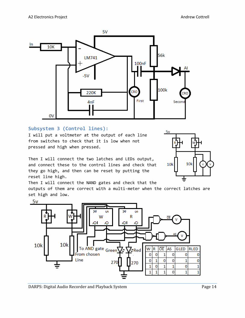
Subsystem 3 (Control lines):.............................................. 8
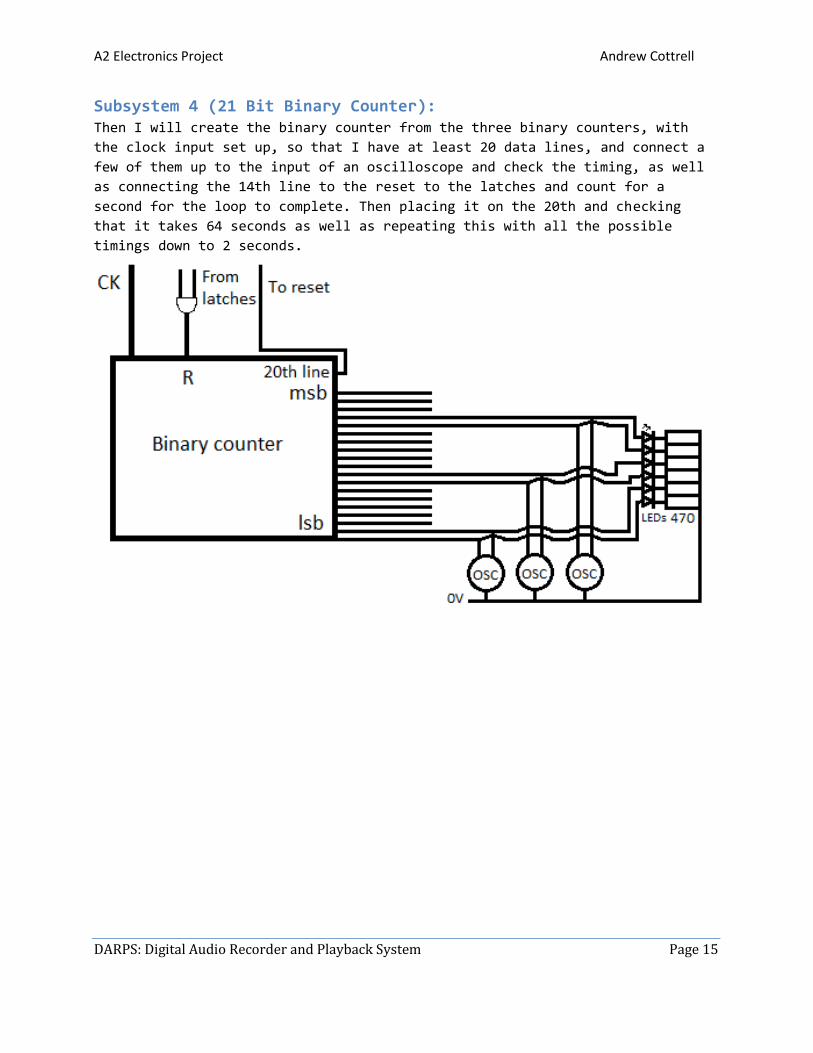
Subsystem 4 (21 Bit Binary Counter): ...................................... 9
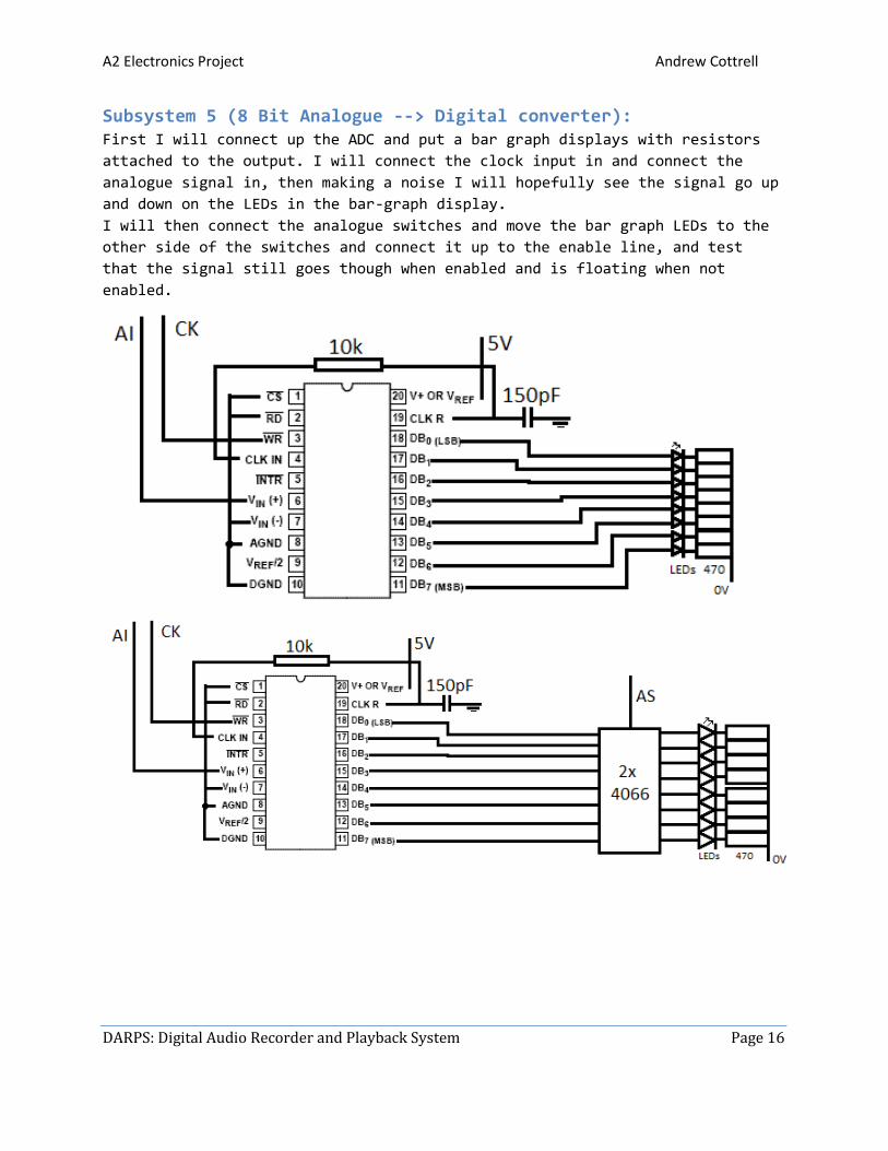
Subsystem 5 (8 Bit Analogue --> Digital Converter and sub-control line): . 10
ADC: .................................................................................................................................................... 10
Sub-control line (WE line): .................................................................................................. 10
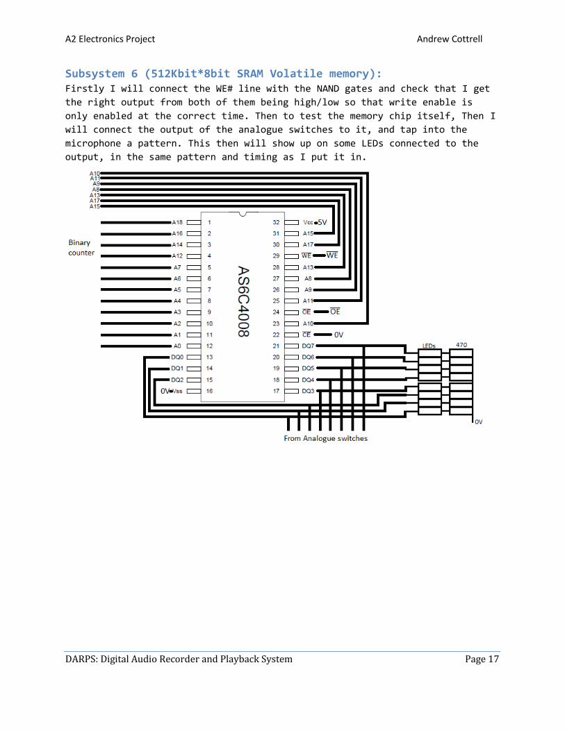
Subsystem 6 (512Kbit*8bit SRAM Volatile memory): ......................... 11
Subsystem 7 (8 Bit Digital --> Analogue converter): ...................... 12
Subsystem 8 (Driver and loudspeaker): .................................... 12
Driver part one: .......................................................................................................................... 12
Driver part two and loudspeaker: ....................................................................................... 12
Testing Regime: ........................................................... 13
Subsystem 1 (8KHz Relaxation Oscillator): ................................ 13
Subsystem 2 (Microphone and Preamp): ..................................... 13
Microphone: ..................................................................................................................................... 13
Preamp: .............................................................................................................................................. 13
A2 Electronics Project Andrew Cottrell
DARPS: Digital Audio Recorder and Playback System Page 2
Subsystem 3 (Control lines):............................................. 14
Subsystem 4 (21 Bit Binary Counter): ..................................... 15
Subsystem 5 (8 Bit Analogue --> Digital converter): ...................... 16
Subsystem 6 (512Kbit*8bit SRAM Volatile memory): ......................... 17
Subsystem 7 (8 Bit Digital --> Analogue converter): ...................... 18
Subsystem 8 (Driver and Loudspeaker): .................................... 18
Driver part one: .......................................................................................................................... 18
Driver part two and loudspeaker: ....................................................................................... 18
Entire System Testing: .................................................. 19
System Testing: ........................................................... 19
Subsystem 1 (8KHz Relaxation Oscillator): ................................ 19
Subsystem 2 (Microphone and Preamp): ..................................... 21
Microphone: ..................................................................................................................................... 21
Preamp: .............................................................................................................................................. 22
Subsystem 3 (Control Lines):............................................. 25
Subsystem 4 (21 Bit Binary Counter): ..................................... 30
Subsystem 5 (8 Bit Analogue --> Digital converter): ...................... 40
Analogue switches:...................................................................................................................... 40
Subsystem 6 (512Kbit*8bit SRAM Volatile Memory) .......................... 45
Subsystem 7 (8 Bit Digital --> Analogue converter): ...................... 47
Output Enable: .............................................................................................................................. 54
Subsystem 8 (Driver and Loudspeaker): .................................... 55
Voltage offset and primary amplifier: ............................................................................ 55
Second amplifier and Loudspeaker: ..................................................................................... 55
Complete System Testing, Analysis and Conclusion ........................... 57
Issues found and their causes: ........................................... 57
What I would do to fix these issues if I had the resources: .............. 60
Overall conclusion of the project: ....................................... 60
Circuit Diagram ........................................................... 62
Photos of Entire Circuit .................................................. 63
Unlabeled ............................................................... 63
Labeled ................................................................. 64
Full component list ....................................................... 65
Bibliography .............................................................. 66
A2 Electronics Project Andrew Cottrell
DARPS: Digital Audio Recorder and Playback System Page 3
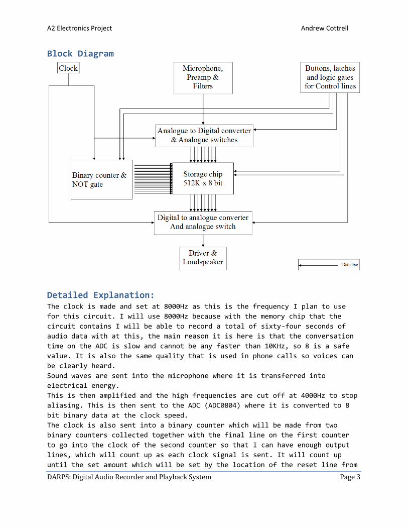
Block Diagram
Detailed Explanation: The clock is made and set at 8000Hz as this is the frequency I plan to use
for this circuit. I will use 8000Hz because with the memory chip that the
circuit contains I will be able to record a total of sixty-four seconds of
audio data with at this, the main reason it is here is that the conversation
time on the ADC is slow and cannot be any faster than 10KHz, so 8 is a safe
value. It is also the same quality that is used in phone calls so voices can
be clearly heard.
Sound waves are sent into the microphone where it is transferred into
electrical energy.
This is then amplified and the high frequencies are cut off at 4000Hz to stop
aliasing. This is then sent to the ADC (ADC0804) where it is converted to 8
bit binary data at the clock speed.
The clock is also sent into a binary counter which will be made from two
binary counters collected together with the final line on the first counter
to go into the clock of the second counter so that I can have enough output
lines, which will count up as each clock signal is sent. It will count up
until the set amount which will be set by the location of the reset line from
A2 Electronics Project Andrew Cottrell
DARPS: Digital Audio Recorder and Playback System Page 4
the dual latches. There will be 19 address lines from the counters to the
address bus on the chip and the 20th line will go initially to the reset on
the latch for full 64 seconds of time. There will be three binary outputs
from this, one that controls the Write enable, one that controls the Output
enable, and one that controls the analogue switches from the ADC to the
memory chip.
When the output is enabled from the memory chip, the 8 bit digital signal is
sent into the DAC (ZN425) which is also running off the same clock signal.
This should create the analogue wave back in between 0 and 5v as it were
before going into the ADC. This then is sent to the driver, which returns the
signal to being between -2.5 and 2.5V and then an op amp will amplify it by a
quarter so that the input levels will be correct for the secondary amplifier
which will amplify it to a maximum of 12V and be able to drive the loud
speaker as it can source a lot more current than the primary amplifier or
DAC.
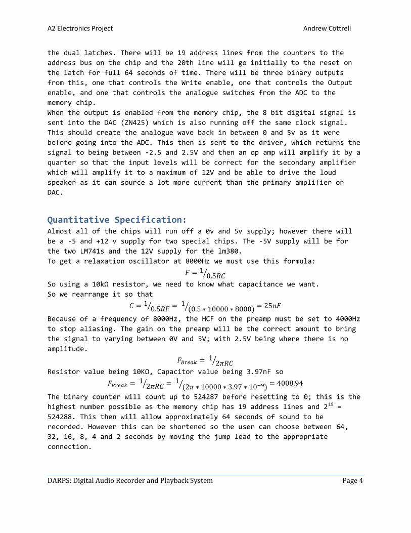
Quantitative Specification: Almost all of the chips will run off a 0v and 5v supply; however there will
be a -5 and +12 v supply for two special chips. The -5V supply will be for
the two LM741s and the 12V supply for the lm380.
To get a relaxation oscillator at 8000Hz we must use this formula:
⁄
So using a 10kΩ resistor, we need to know what capacitance we want.
So we rearrange it so that
⁄ ⁄
Because of a frequency of 8000Hz, the HCF on the preamp must be set to 4000Hz
to stop aliasing. The gain on the preamp will be the correct amount to bring
the signal to varying between 0V and 5V; with 2.5V being where there is no
amplitude.
⁄
Resistor value being 10KΩ, Capacitor value being 3.97nF so
⁄ ⁄
The binary counter will count up to 524287 before resetting to 0; this is the
highest number possible as the memory chip has 19 address lines and 219 =
524288. This then will allow approximately 64 seconds of sound to be
recorded. However this can be shortened so the user can choose between 64,
32, 16, 8, 4 and 2 seconds by moving the jump lead to the appropriate
connection.
A2 Electronics Project Andrew Cottrell
DARPS: Digital Audio Recorder and Playback System Page 5
The preamp needs to bring the signal from a peak of 0.1v to 2.5v, so the
maximum gain we want is 25. For a safe value I chose 22 but as it is an
inverting amplifier this is a negative. So to get -22 we must use
After the amplifier there needs to be a voltage offset of 3.2V, this is
worked out by wanting to have a voltage offset of 2.5v, but after this it
goes through a diode which drops 0.7v, so we need to add this onto the
offset. This means that we need to make a potential divider which has 3.2v in
the middle.
To do this we use ohms law to work out the current across the entire
potential divider if we use 100k and 56k resistors. This comes out to be
32μA, which then across the bottom resistor gives 3.205V for an offset.
However, when this is connected you make a subtle low cut filter. So we need
to make sure the capacitor is a value which does not interfere with this
circuit. For this we also use
⁄
We will use 15Hz as an acceptable value for the frequency to be cut at as
this is below what we can hear.
Rearranging the equation:
⁄
⁄ ⁄
Around 1.06E-7. This is approximately 100nF.
For the hold down resistors I use 10K because this is a value which will not
draw too much current through the circuit. If it was a lower resistance the
power would be higher and the circuit less efficient.
My data will be 8bit for many reasons; firstly 8 bit gives me 256 voltage
levels, which when between 0 and 5v means that the resolution is 0.02V per
division. Secondly the chips all support 8 bit and if it were any higher than
8 bit I would have even more issues with keeping the wiring neat.
For using LEDS when testing I will use a 470 Ohm resistor for each LED so
that this may limit the current sufficiently enough to make sure that a led
will not be damaged with 5v. V=IR,
- perfect for an LED.
For the LEDs actually in the circuit I will use 270 Ohms because this allows
20mA (
) which allows the LEDs to glow without being damaged but
brighter.
The values for the self-clocking of the ADC were given to me by its
datasheet.
For the voltage offset which will bring the signal back to varying around 0v,
we use a basic RC circuit; however we need to make sure that this circuit
A2 Electronics Project Andrew Cottrell
DARPS: Digital Audio Recorder and Playback System Page 6
does not also turn into a low cut filter that would affect the system. To do
this we use a high resistance resistor (330k) and then the formula
⁄
Using a 470nF Capacitor it cuts the frequency at a very safe 1.026Hz
For the first op-amp in the driver; I need a gain of –¼. To work this out we
use
. This is
⁄ . This is close enough to ¼ and will
work well. It will need a +5 and -5 power supply.
The second Amplifier and loud speaker will need a 12V and 0V power supply,
and the gain is controlled by the potentiometer.
Research and Circuit Diagrams:
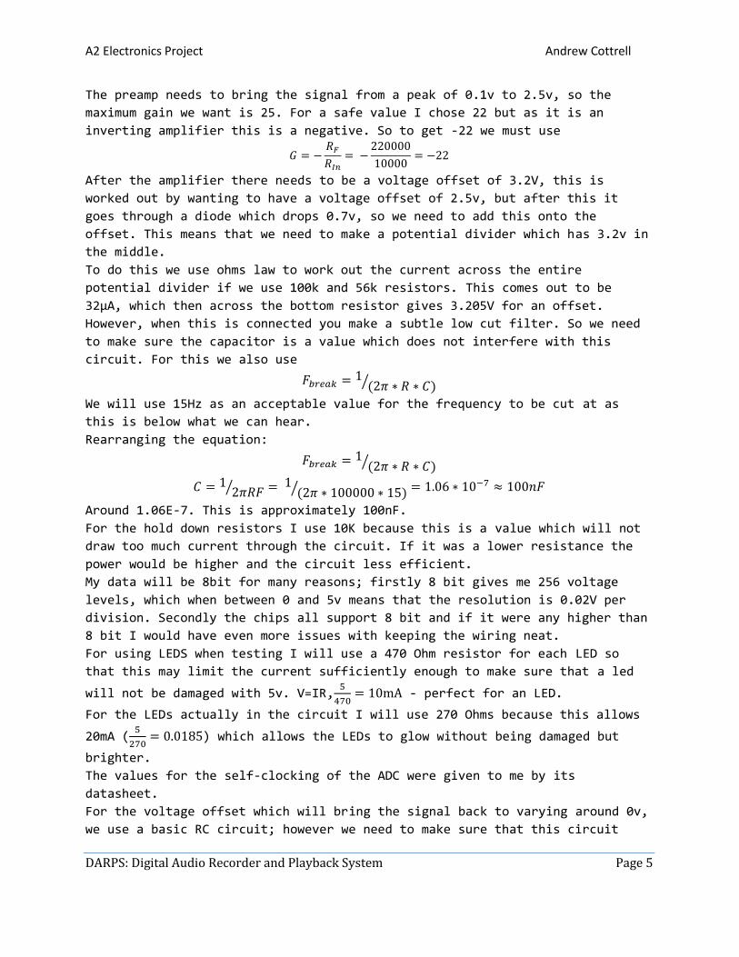
Subsystem 1 (8KHz Relaxation Oscillator):
These values would produce a nice frequency for the
clock. The clock does not need an enable input as
the control of the device will be handled a
different method instead of clock control.
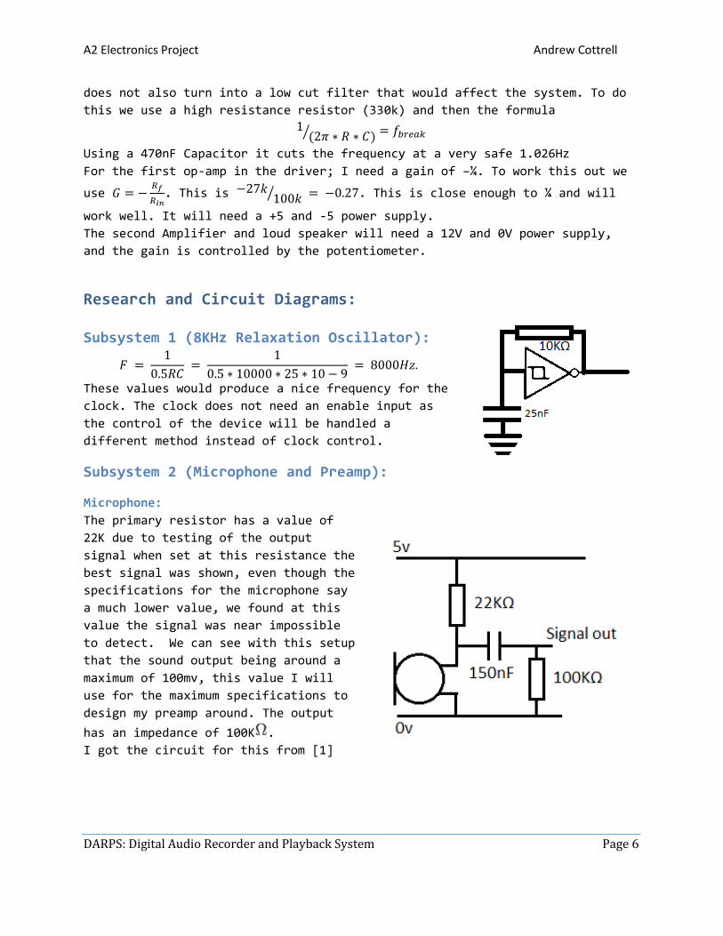
Subsystem 2 (Microphone and Preamp):
Microphone:
The primary resistor has a value of
22K due to testing of the output
signal when set at this resistance the
best signal was shown, even though the
specifications for the microphone say
a much lower value, we found at this
value the signal was near impossible
to detect. We can see with this setup
that the sound output being around a
maximum of 100mv, this value I will
use for the maximum specifications to
design my preamp around. The output
has an impedance of 100K .
I got the circuit for this from [1]
A2 Electronics Project Andrew Cottrell
DARPS: Digital Audio Recorder and Playback System Page 7
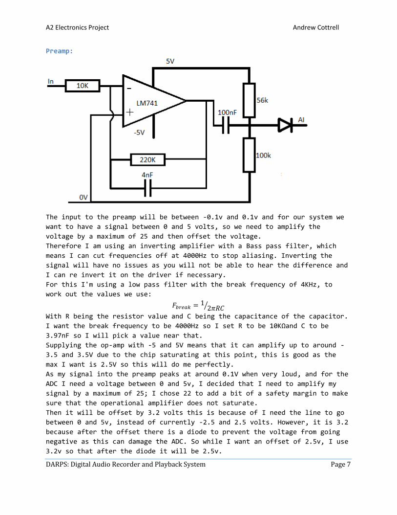
Preamp:
The input to the preamp will be between -0.1v and 0.1v and for our system we
want to have a signal between 0 and 5 volts, so we need to amplify the
voltage by a maximum of 25 and then offset the voltage.
Therefore I am using an inverting amplifier with a Bass pass filter, which
means I can cut frequencies off at 4000Hz to stop aliasing. Inverting the
signal will have no issues as you will not be able to hear the difference and
I can re invert it on the driver if necessary.
For this I'm using a low pass filter with the break frequency of 4KHz, to
work out the values we use:
⁄
With R being the resistor value and C being the capacitance of the capacitor.
I want the break frequency to be 4000Hz so I set R to be 10KΩand C to be
3.97nF so I will pick a value near that.
Supplying the op-amp with -5 and 5V means that it can amplify up to around -
3.5 and 3.5V due to the chip saturating at this point, this is good as the
max I want is 2.5V so this will do me perfectly.
As my signal into the preamp peaks at around 0.1V when very loud, and for the
ADC I need a voltage between 0 and 5v, I decided that I need to amplify my
signal by a maximum of 25; I chose 22 to add a bit of a safety margin to make
sure that the operational amplifier does not saturate.
Then it will be offset by 3.2 volts this is because of I need the line to go
between 0 and 5v, instead of currently -2.5 and 2.5 volts. However, it is 3.2
because after the offset there is a diode to prevent the voltage from going
negative as this can damage the ADC. So while I want an offset of 2.5v, I use
3.2v so that after the diode it will be 2.5v.
A2 Electronics Project Andrew Cottrell
DARPS: Digital Audio Recorder and Playback System Page 8
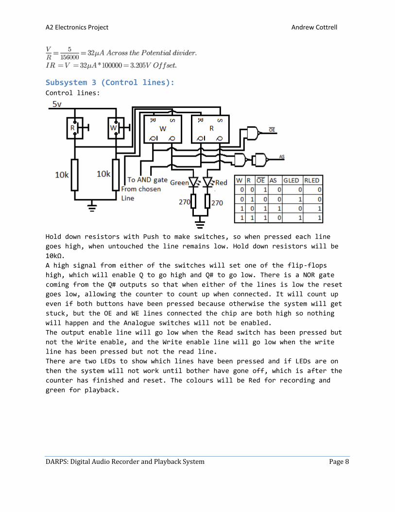
Subsystem 3 (Control lines): Control lines:
Hold down resistors with Push to make switches, so when pressed each line
goes high, when untouched the line remains low. Hold down resistors will be
10kΩ.
A high signal from either of the switches will set one of the flip-flops
high, which will enable Q to go high and Q# to go low. There is a NOR gate
coming from the Q# outputs so that when either of the lines is low the reset
goes low, allowing the counter to count up when connected. It will count up
even if both buttons have been pressed because otherwise the system will get
stuck, but the OE and WE lines connected the chip are both high so nothing
will happen and the Analogue switches will not be enabled.
The output enable line will go low when the Read switch has been pressed but
not the Write enable, and the Write enable line will go low when the write
line has been pressed but not the read line.
There are two LEDs to show which lines have been pressed and if LEDs are on
then the system will not work until bother have gone off, which is after the
counter has finished and reset. The colours will be Red for recording and
green for playback.

A2 Electronics Project Andrew Cottrell
DARPS: Digital Audio Recorder and Playback System Page 9
Subsystem 4 (21 Bit Binary Counter): The counter counts up on falling
edge of the clock pulse, and then
counts up until it reaches its
maximum. Then as the maximum line
falls low it triggers a clock
pulse on the next counter and this
repeats until the address is high
enough to enable the reset on the
main system to be activated.
Having the first input active low
is important because it means once
the counter has reached the top
of its counts, as the MSB goes
low, the clock on the next
counter goes up.
The reset line goes to the
latches from the chosen pin on
the counters. If full 64
seconds is wanted, then you
chose the 19th address line, 32
seconds the 18th, etc.
A2 Electronics Project Andrew Cottrell
DARPS: Digital Audio Recorder and Playback System Page 10
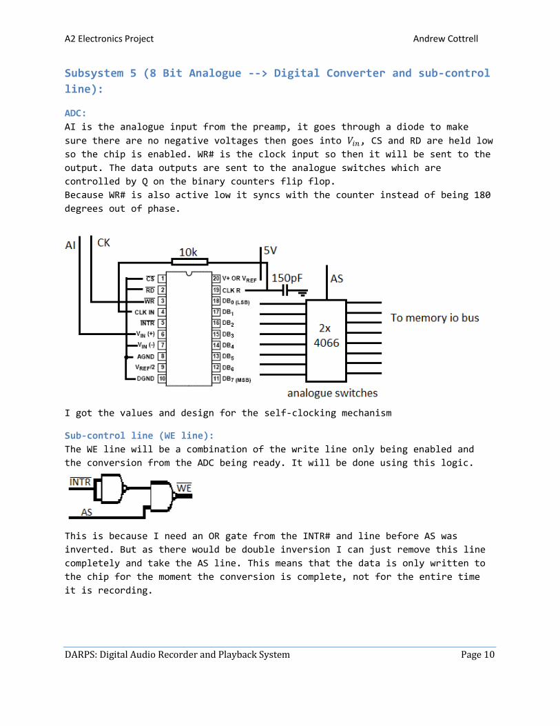
Subsystem 5 (8 Bit Analogue --> Digital Converter and sub-control
line):
ADC:
AI is the analogue input from the preamp, it goes through a diode to make
sure there are no negative voltages then goes into , CS and RD are held low
so the chip is enabled. WR# is the clock input so then it will be sent to the
output. The data outputs are sent to the analogue switches which are
controlled by Q on the binary counters flip flop.
Because WR# is also active low it syncs with the counter instead of being 180
degrees out of phase.
I got the values and design for the self-clocking mechanism
Sub-control line (WE line):
The WE line will be a combination of the write line only being enabled and
the conversion from the ADC being ready. It will be done using this logic.
This is because I need an OR gate from the INTR# and line before AS was
inverted. But as there would be double inversion I can just remove this line
completely and take the AS line. This means that the data is only written to
the chip for the moment the conversion is complete, not for the entire time
it is recording.
A2 Electronics Project Andrew Cottrell
DARPS: Digital Audio Recorder and Playback System Page 11
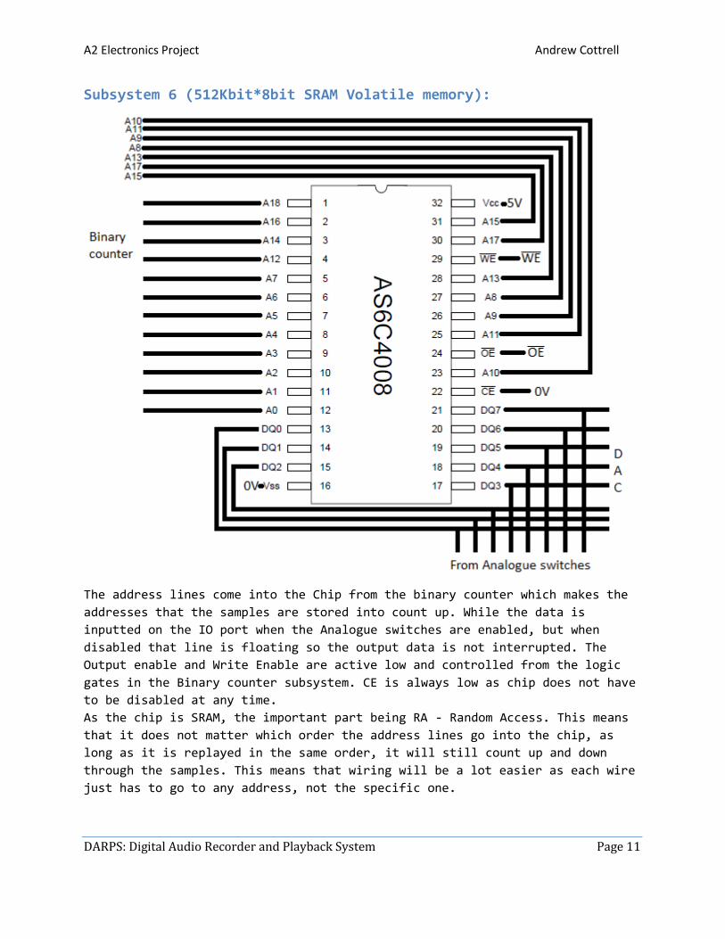
Subsystem 6 (512Kbit*8bit SRAM Volatile memory):
The address lines come into the Chip from the binary counter which makes the
addresses that the samples are stored into count up. While the data is
inputted on the IO port when the Analogue switches are enabled, but when
disabled that line is floating so the output data is not interrupted. The
Output enable and Write Enable are active low and controlled from the logic
gates in the Binary counter subsystem. CE is always low as chip does not have
to be disabled at any time.
As the chip is SRAM, the important part being RA - Random Access. This means
that it does not matter which order the address lines go into the chip, as
long as it is replayed in the same order, it will still count up and down
through the samples. This means that wiring will be a lot easier as each wire
just has to go to any address, not the specific one.
A2 Electronics Project Andrew Cottrell
DARPS: Digital Audio Recorder and Playback System Page 12
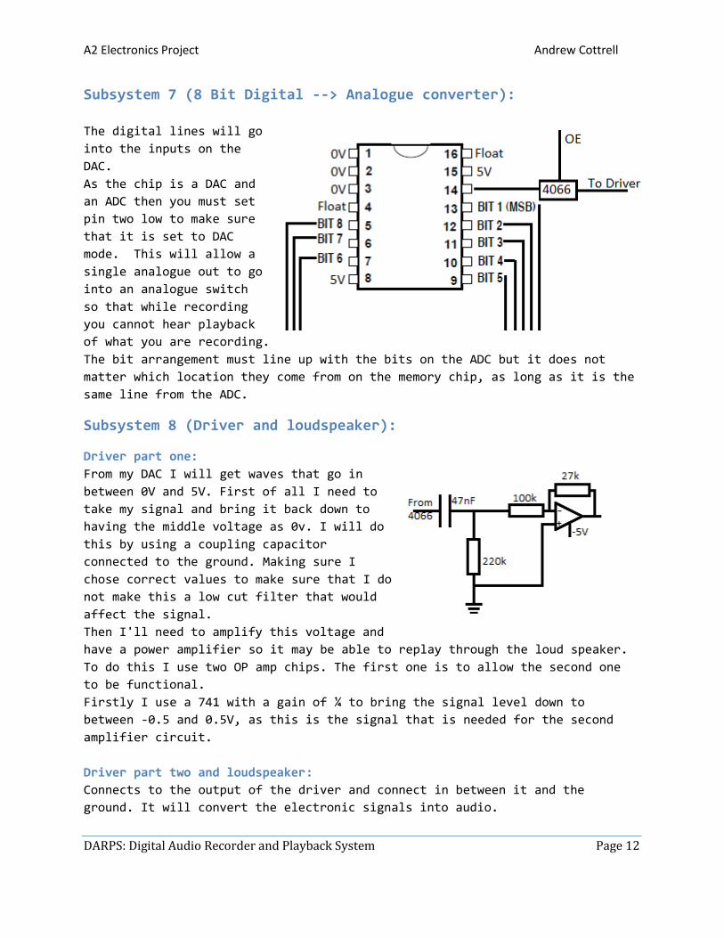
Subsystem 7 (8 Bit Digital --> Analogue converter):
The digital lines will go
into the inputs on the
DAC.
As the chip is a DAC and
an ADC then you must set
pin two low to make sure
that it is set to DAC
mode. This will allow a
single analogue out to go
into an analogue switch
so that while recording
you cannot hear playback
of what you are recording.
The bit arrangement must line up with the bits on the ADC but it does not
matter which location they come from on the memory chip, as long as it is the
same line from the ADC.
Subsystem 8 (Driver and loudspeaker):
Driver part one:
From my DAC I will get waves that go in
between 0V and 5V. First of all I need to
take my signal and bring it back down to
having the middle voltage as 0v. I will do
this by using a coupling capacitor
connected to the ground. Making sure I
chose correct values to make sure that I do
not make this a low cut filter that would
affect the signal.
Then I'll need to amplify this voltage and
have a power amplifier so it may be able to replay through the loud speaker.
To do this I use two OP amp chips. The first one is to allow the second one
to be functional.
Firstly I use a 741 with a gain of ¼ to bring the signal level down to
between -0.5 and 0.5V, as this is the signal that is needed for the second
amplifier circuit.
Driver part two and loudspeaker:
Connects to the output of the driver and connect in between it and the
ground. It will convert the electronic signals into audio.
A2 Electronics Project Andrew Cottrell
DARPS: Digital Audio Recorder and Playback System Page 13
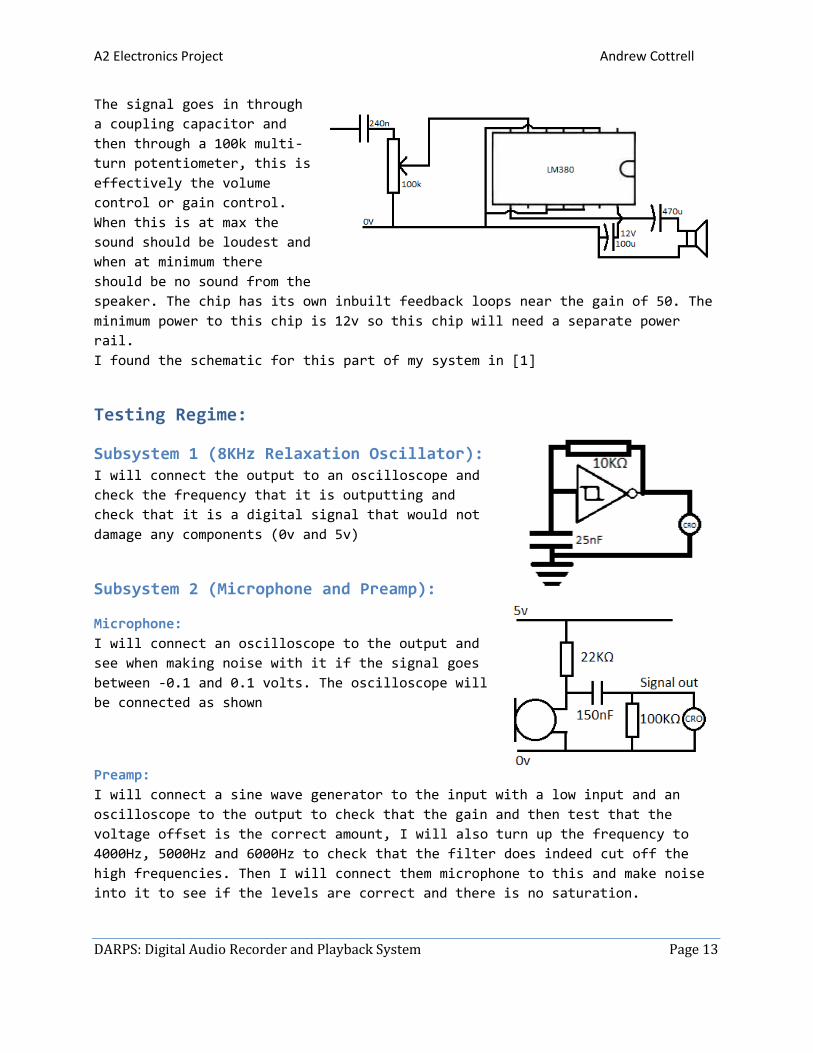
The signal goes in through
a coupling capacitor and
then through a 100k multi-
turn potentiometer, this is
effectively the volume
control or gain control.
When this is at max the
sound should be loudest and
when at minimum there
should be no sound from the
speaker. The chip has its own inbuilt feedback loops near the gain of 50. The
minimum power to this chip is 12v so this chip will need a separate power
rail.
I found the schematic for this part of my system in [1]
Testing Regime:
Subsystem 1 (8KHz Relaxation Oscillator): I will connect the output to an oscilloscope and
check the frequency that it is outputting and
check that it is a digital signal that would not
damage any components (0v and 5v)
Subsystem 2 (Microphone and Preamp):
Microphone:
I will connect an oscilloscope to the output and
see when making noise with it if the signal goes
between -0.1 and 0.1 volts. The oscilloscope will
be connected as shown
Preamp:
I will connect a sine wave generator to the input with a low input and an
oscilloscope to the output to check that the gain and then test that the
voltage offset is the correct amount, I will also turn up the frequency to
4000Hz, 5000Hz and 6000Hz to check that the filter does indeed cut off the
high frequencies. Then I will connect them microphone to this and make noise
into it to see if the levels are correct and there is no saturation.
A2 Electronics Project Andrew Cottrell
DARPS: Digital Audio Recorder and Playback System Page 14
Subsystem 3 (Control lines): I will put a voltmeter at the output of each line
from switches to check that it is low when not
pressed and high when pressed.
Then I will connect the two latches and LEDs output,
and connect these to the control lines and check that
they go high, and then can be reset by putting the
reset line high.
Then I will connect the NAND gates and check that the
outputs of them are correct with a multi-meter when the correct latches are
set high and low.
A2 Electronics Project Andrew Cottrell
DARPS: Digital Audio Recorder and Playback System Page 15
Subsystem 4 (21 Bit Binary Counter): Then I will create the binary counter from the three binary counters, with
the clock input set up, so that I have at least 20 data lines, and connect a
few of them up to the input of an oscilloscope and check the timing, as well
as connecting the 14th line to the reset to the latches and count for a
second for the loop to complete. Then placing it on the 20th and checking
that it takes 64 seconds as well as repeating this with all the possible
timings down to 2 seconds.
A2 Electronics Project Andrew Cottrell
DARPS: Digital Audio Recorder and Playback System Page 16
Subsystem 5 (8 Bit Analogue --> Digital converter): First I will connect up the ADC and put a bar graph displays with resistors
attached to the output. I will connect the clock input in and connect the
analogue signal in, then making a noise I will hopefully see the signal go up
and down on the LEDs in the bar-graph display.
I will then connect the analogue switches and move the bar graph LEDs to the
other side of the switches and connect it up to the enable line, and test
that the signal still goes though when enabled and is floating when not
enabled.
A2 Electronics Project Andrew Cottrell
DARPS: Digital Audio Recorder and Playback System Page 17
Subsystem 6 (512Kbit*8bit SRAM Volatile memory): Firstly I will connect the WE# line with the NAND gates and check that I get
the right output from both of them being high/low so that write enable is
only enabled at the correct time. Then to test the memory chip itself, Then I
will connect the output of the analogue switches to it, and tap into the
microphone a pattern. This then will show up on some LEDs connected to the
output, in the same pattern and timing as I put it in.

A2 Electronics Project Andrew Cottrell
DARPS: Digital Audio Recorder and Playback System Page 18
Subsystem 7 (8 Bit Digital --> Analogue converter): I will connect up
the DAC chip and
then connect 8
jump leads to the
inputs; first with
them all grounded
and then change
each one
individually with
a volt meter on
the output check
to the voltage is
correct for the binary input. Then I will connect it to the memory chip and
check that it outputs the stored pattern correctly.
Then I will connect up an oscilloscope on the output and the input to the ADC
and see how different the signal is between the two.
Subsystem 8 (Driver and Loudspeaker):
Driver part one:
Firstly I will test that the voltage is brought
down from in-between 0v and 5v to -2.5v and
2.5v. To do this I will connect up an
oscilloscope both sides of the RC circuit. Then
I will connect the signal into the op-amp and
out the other side and check that the gain and
signal levels are the correct amount.
I will do this my connecting an oscilloscope to
the input and output of the op amp.
Driver part two and loudspeaker:
Then with this signal I will put
it through the potentiometer and
into the second amplifier, and on
the output I will put the
loudspeaker. I will input a small
sine wave into the amplifier with
the same output levels as the
first amplifier from a signal
generator and see if the sound is

A2 Electronics Project Andrew Cottrell
DARPS: Digital Audio Recorder and Playback System Page 19
displayed.
To test the loudspeaker I will first check that the value
of impedance I have for it is correct by connecting it to
an ohm meter. Then I will connect it to a signal generator
to hear if it makes a noise and the pitch changes as the
frequency does.
Entire System Testing: Then I will connect a sine wave from a signal generator into the input of the
ADC, and record this into the system, changing the frequencies, and then I
will replay this sound and listen to the output of the speaker. If this is
successful I will speak into the microphone and then listen to it playing
back. I will also connect an oscilloscope on the sine wave to see difference
between the input and output wave.
System Testing:
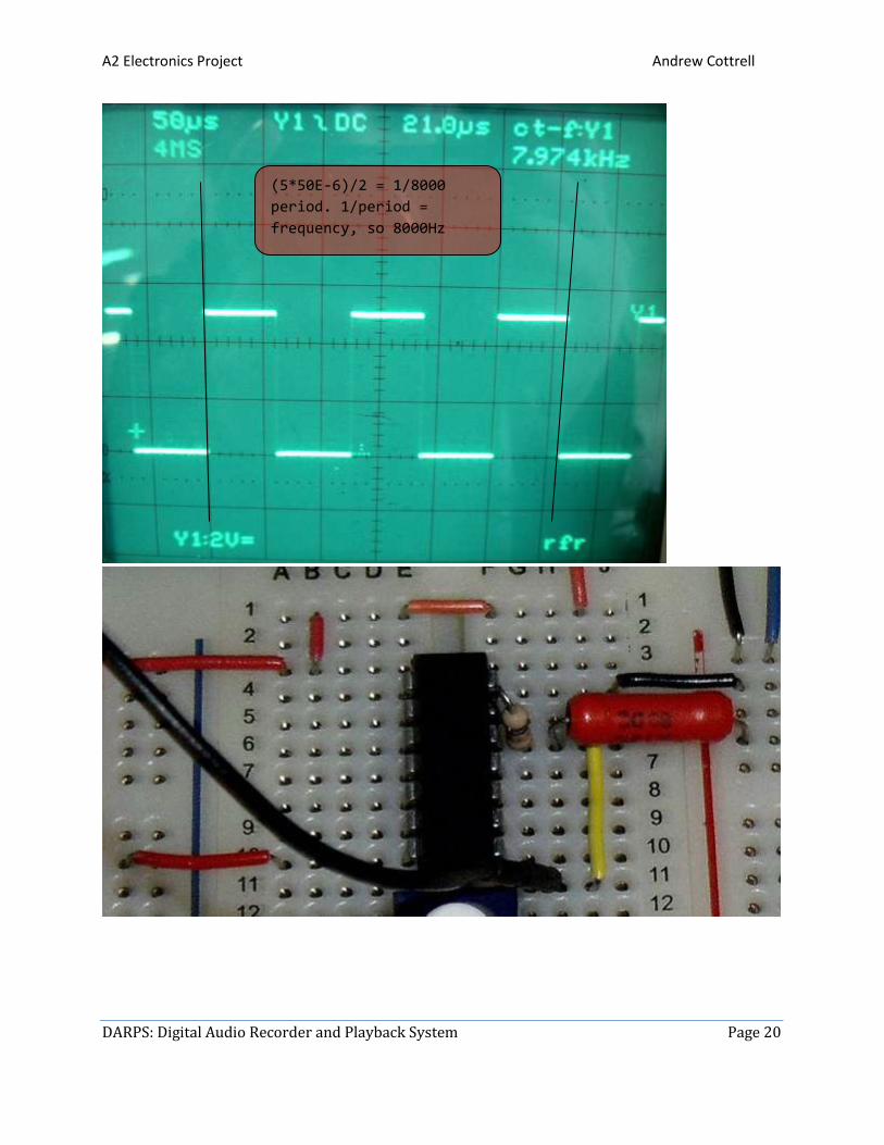
Subsystem 1 (8KHz Relaxation Oscillator): Firstly I connected up my values, but I noticed that the frequency was not
what I expected it to be.
So I changed the values around in the circuit, and managed to find a
capacitor which gave me a much closer value to 8000Hz.
I then connected up the clock with the new values which while the formula did
not agree with, but this brought me closest to the 8KHz mark I wanted.
We can work out the frequency of the clock by first working out the period,
you can see it takes up 5 squares for two periods, so 2.5
squares at 50uS means that a period is 50*2.5 = 125uS,
then you put 1/(125E-6) and you get exactly 8000Hz.
However as the oscilloscope can measure more accurately
than we can see, it sees the frequency as 7.974KHz, which
is very close to 8KHz.
Now if we do some calculations we can work out that the
time that could be recorded on the maximum rate:
T= Max number of samples / Samples per second = 524288/7974 = 65.75 Seconds
of recording and playback time.
A2 Electronics Project Andrew Cottrell
DARPS: Digital Audio Recorder and Playback System Page 20
(5*50E-6)/2 = 1/8000
period. 1/period =
frequency, so 8000Hz
A2 Electronics Project Andrew Cottrell
DARPS: Digital Audio Recorder and Playback System Page 21
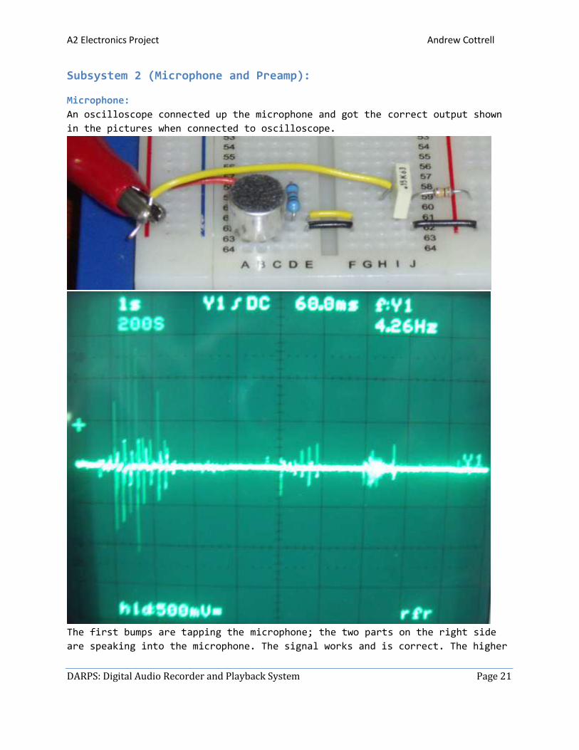
Subsystem 2 (Microphone and Preamp):
Microphone:
An oscilloscope connected up the microphone and got the correct output shown
in the pictures when connected to oscilloscope.
The first bumps are tapping the microphone; the two parts on the right side
are speaking into the microphone. The signal works and is correct. The higher
A2 Electronics Project Andrew Cottrell
DARPS: Digital Audio Recorder and Playback System Page 22
voltages are not to be worried about as they will just saturate in the
preamp.
Preamp:
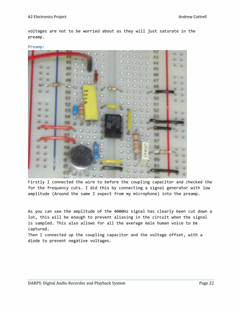
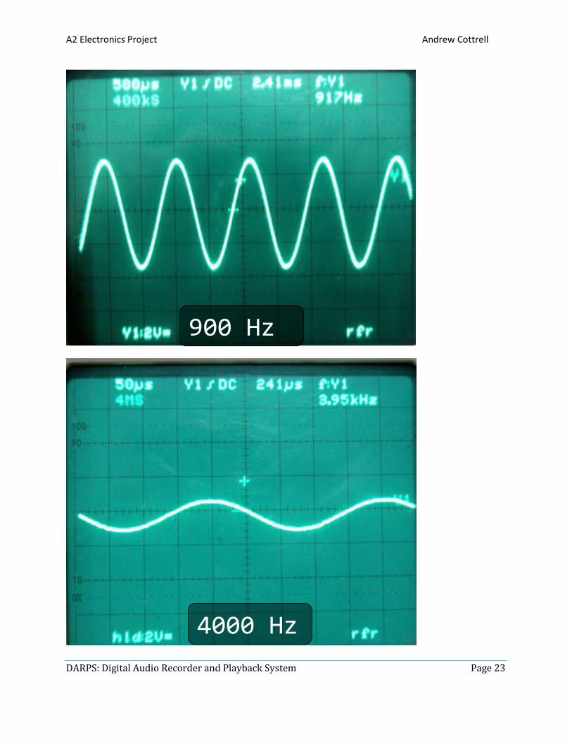
Firstly I connected the wire to before the coupling capacitor and checked the
for the frequency cuts. I did this by connecting a signal generator with low
amplitude (Around the same I expect from my microphone) into the preamp.
As you can see the amplitude of the 4000Hz signal has clearly been cut down a
lot, this will be enough to prevent aliasing in the circuit when the signal
is sampled. This also allows for all the average male human voice to be
captured.
Then I connected up the coupling capacitor and the voltage offset, with a
diode to prevent negative voltages.
A2 Electronics Project Andrew Cottrell
DARPS: Digital Audio Recorder and Playback System Page 23
900 Hz
4000 Hz

A2 Electronics Project Andrew Cottrell
DARPS: Digital Audio Recorder and Playback System Page 24
This is where I was
tapping on the
microphone; on the very
left you can see where 0v
is, before I connected
the signal. The voltage
offsets at around 2.4v
which is about right. The
slightly lower is
probably due to the diode
taking more than 0.7v
This is where I made loud
noises to test the limit.
As you see the chip will
not go much below -0.4V,
so the chip cannot be
damaged, as well as this
it will not go much above
5 volts so the chip is
safe.
A2 Electronics Project Andrew Cottrell
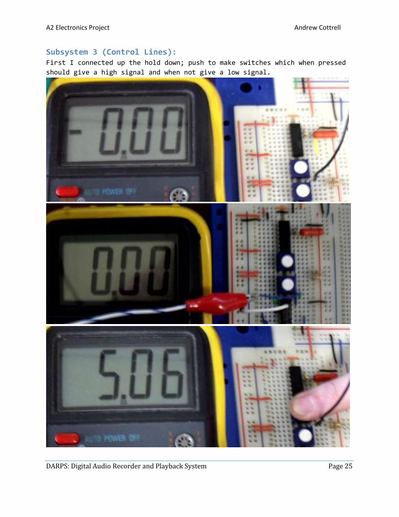
DARPS: Digital Audio Recorder and Playback System Page 25
Subsystem 3 (Control Lines): First I connected up the hold down; push to make switches which when pressed
should give a high signal and when not give a low signal.
A2 Electronics Project Andrew Cottrell
DARPS: Digital Audio Recorder and Playback System Page 26
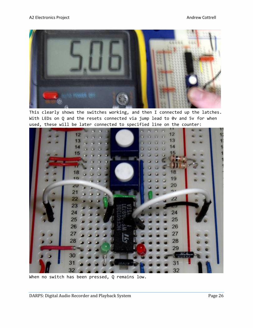
This clearly shows the switches working, and then I connected up the latches.
With LEDs on Q and the resets connected via jump lead to 0v and 5v for when
used, these will be later connected to specified line on the counter:
When no switch has been pressed, Q remains low.
A2 Electronics Project Andrew Cottrell
DARPS: Digital Audio Recorder and Playback System Page 27
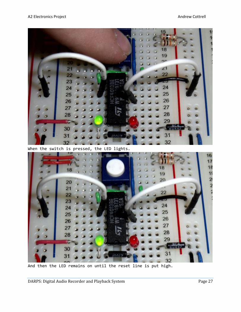
When the switch is pressed, the LED lights.
And then the LED remains on until the reset line is put high.
A2 Electronics Project Andrew Cottrell
DARPS: Digital Audio Recorder and Playback System Page 28
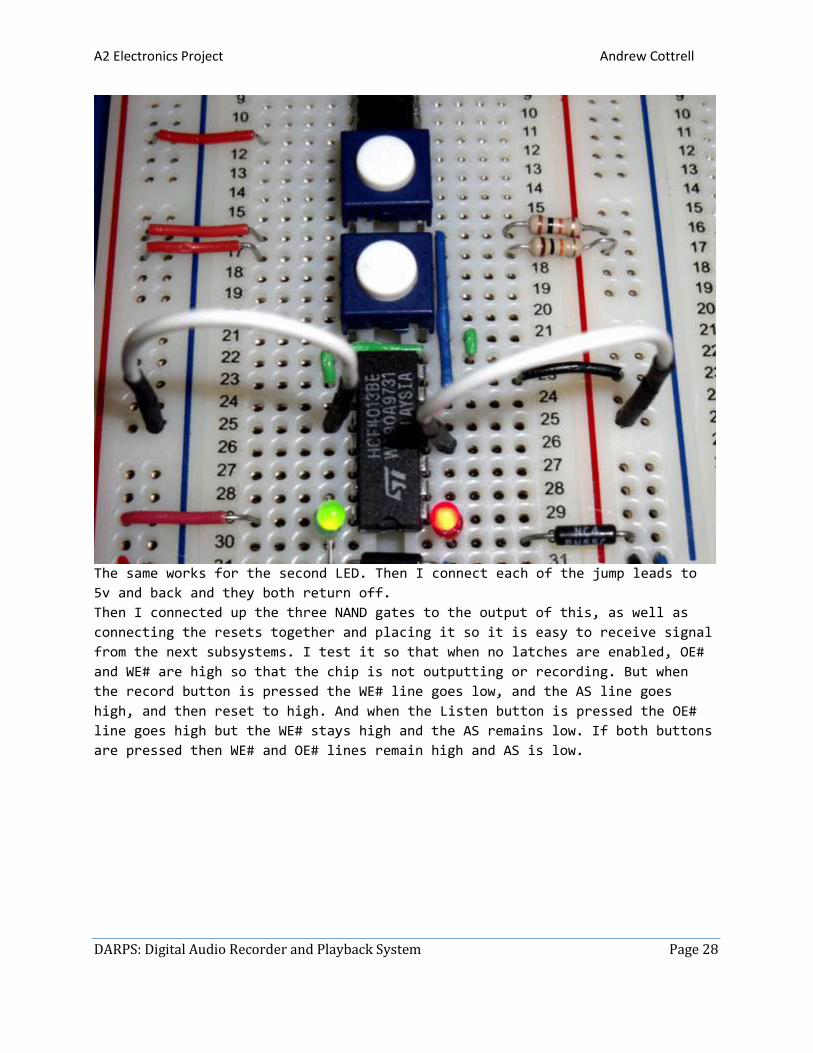
The same works for the second LED. Then I connect each of the jump leads to
5v and back and they both return off.
Then I connected up the three NAND gates to the output of this, as well as
connecting the resets together and placing it so it is easy to receive signal
from the next subsystems. I test it so that when no latches are enabled, OE#
and WE# are high so that the chip is not outputting or recording. But when
the record button is pressed the WE# line goes low, and the AS line goes
high, and then reset to high. And when the Listen button is pressed the OE#
line goes high but the WE# stays high and the AS remains low. If both buttons
are pressed then WE# and OE# lines remain high and AS is low.
A2 Electronics Project Andrew Cottrell
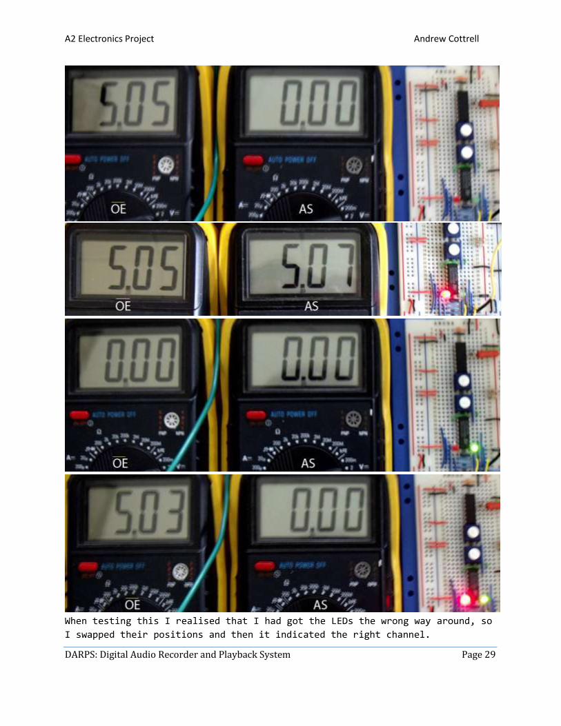
DARPS: Digital Audio Recorder and Playback System Page 29
When testing this I realised that I had got the LEDs the wrong way around, so
I swapped their positions and then it indicated the right channel.
A2 Electronics Project Andrew Cottrell
DARPS: Digital Audio Recorder and Playback System Page 30
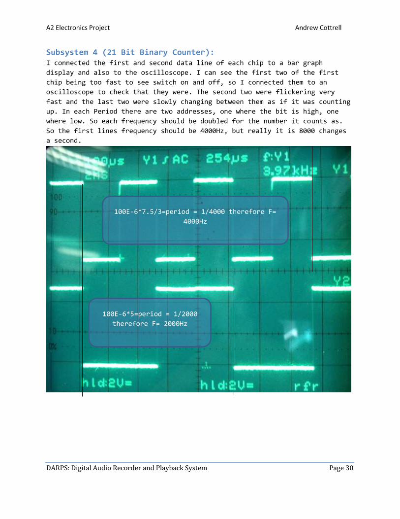
Subsystem 4 (21 Bit Binary Counter): I connected the first and second data line of each chip to a bar graph
display and also to the oscilloscope. I can see the first two of the first
chip being too fast to see switch on and off, so I connected them to an
oscilloscope to check that they were. The second two were flickering very
fast and the last two were slowly changing between them as if it was counting
up. In each Period there are two addresses, one where the bit is high, one
where low. So each frequency should be doubled for the number it counts as.
So the first lines frequency should be 4000Hz, but really it is 8000 changes
a second.
100E-6*7.5/3=period = 1/4000 therefore F=
4000Hz
100E-6*5=period = 1/2000
therefore F= 2000Hz
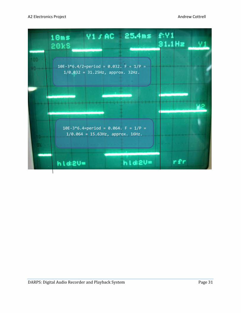
A2 Electronics Project Andrew Cottrell
DARPS: Digital Audio Recorder and Playback System Page 31
10E-3*6.4/2=period = 0.032. F = 1/P =
1/0.032 = 31.25Hz, approx. 32Hz.
10E-3*6.4=period = 0.064. F = 1/P =
1/0.064 = 15.63Hz, approx. 16Hz.
A2 Electronics Project Andrew Cottrell
DARPS: Digital Audio Recorder and Playback System Page 32
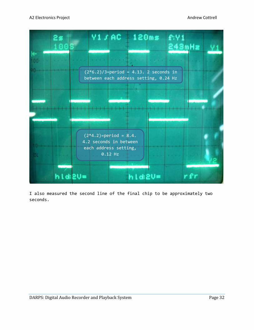
I also measured the second line of the final chip to be approximately two
seconds.
(2*6.2)/3=period = 4.13. 2 seconds in
between each address setting, 0.24 Hz
(2*4.2)=period = 8.4.
4.2 seconds in between
each address setting,
0.12 Hz
A2 Electronics Project Andrew Cottrell
DARPS: Digital Audio Recorder and Playback System Page 33
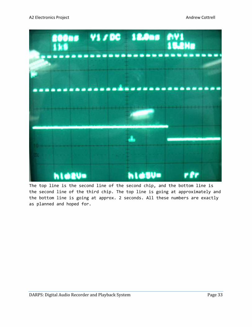
The top line is the second line of the second chip, and the bottom line is
the second line of the third chip. The top line is going at approximately and
the bottom line is going at approx. 2 seconds. All these numbers are exactly
as planned and hoped for.
A2 Electronics Project Andrew Cottrell
DARPS: Digital Audio Recorder and Playback System Page 34
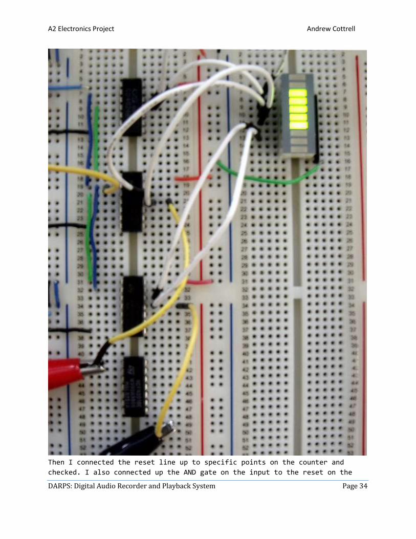
Then I connected the reset line up to specific points on the counter and
checked. I also connected up the AND gate on the input to the reset on the

A2 Electronics Project Andrew Cottrell
DARPS: Digital Audio Recorder and Playback System Page 35
counter. I then tested pressing each button and seeing the signal count up
for the time until reaching the point, and then stopping until the other or
next button is pressed. I set the timer for the first line of the 3rd
counter. This lasts for approx. 2 seconds.
The counting wire is set to the 4th line from the second counter.
Seeing this successfully work I now know that my control lines and counter
work perfectly with the record and playback time set-able by moving a jump
wire.
A2 Electronics Project Andrew Cottrell
DARPS: Digital Audio Recorder and Playback System Page 36
A2 Electronics Project Andrew Cottrell
DARPS: Digital Audio Recorder and Playback System Page 37
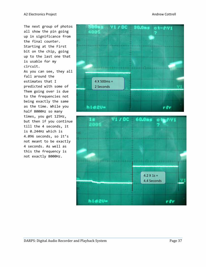
The next group of photos
all show the pin going
up in significance from
the final counter.
Starting at the First
bit on the chip, going
up to the last one that
is usable for my
circuit.
As you can see, they all
fall around the
estimates that I
predicted with some of
Them going over is due
to the frequencies not
being exactly the same
as the time. While you
half 8000Hz so many
times, you get 125Hz,
but then if you continue
till the 4 seconds, it
is 0.244Hz which is
4.096 seconds, so it’s
not meant to be exactly
4 seconds. As well as
this the frequency is
not exactly 8000Hz.
4 X 500ms =
2 Seconds
4.2 X 1s =
4.4 Seconds
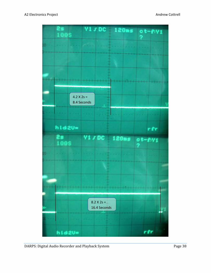
A2 Electronics Project Andrew Cottrell
DARPS: Digital Audio Recorder and Playback System Page 38
4.2 X 2s =
8.4 Seconds
8.2 X 2s =
16.4 Seconds

A2 Electronics Project Andrew Cottrell
DARPS: Digital Audio Recorder and Playback System Page 39
6.6 X 10s =
66 Seconds
6.6 X 5s =
33 Seconds
A2 Electronics Project Andrew Cottrell
DARPS: Digital Audio Recorder and Playback System Page 40
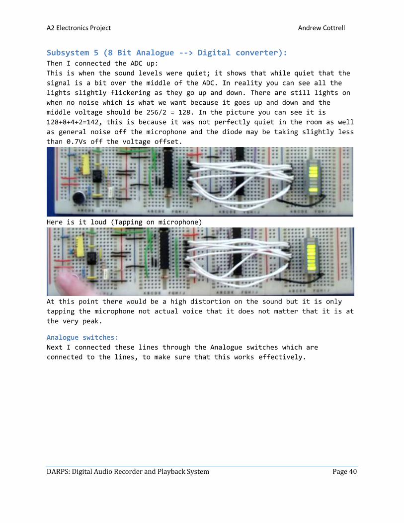
Subsystem 5 (8 Bit Analogue --> Digital converter): Then I connected the ADC up:
This is when the sound levels were quiet; it shows that while quiet that the
signal is a bit over the middle of the ADC. In reality you can see all the
lights slightly flickering as they go up and down. There are still lights on
when no noise which is what we want because it goes up and down and the
middle voltage should be 256/2 = 128. In the picture you can see it is
128+8+4+2=142, this is because it was not perfectly quiet in the room as well
as general noise off the microphone and the diode may be taking slightly less
than 0.7Vs off the voltage offset.
Here is it loud (Tapping on microphone)
At this point there would be a high distortion on the sound but it is only
tapping the microphone not actual voice that it does not matter that it is at
the very peak.
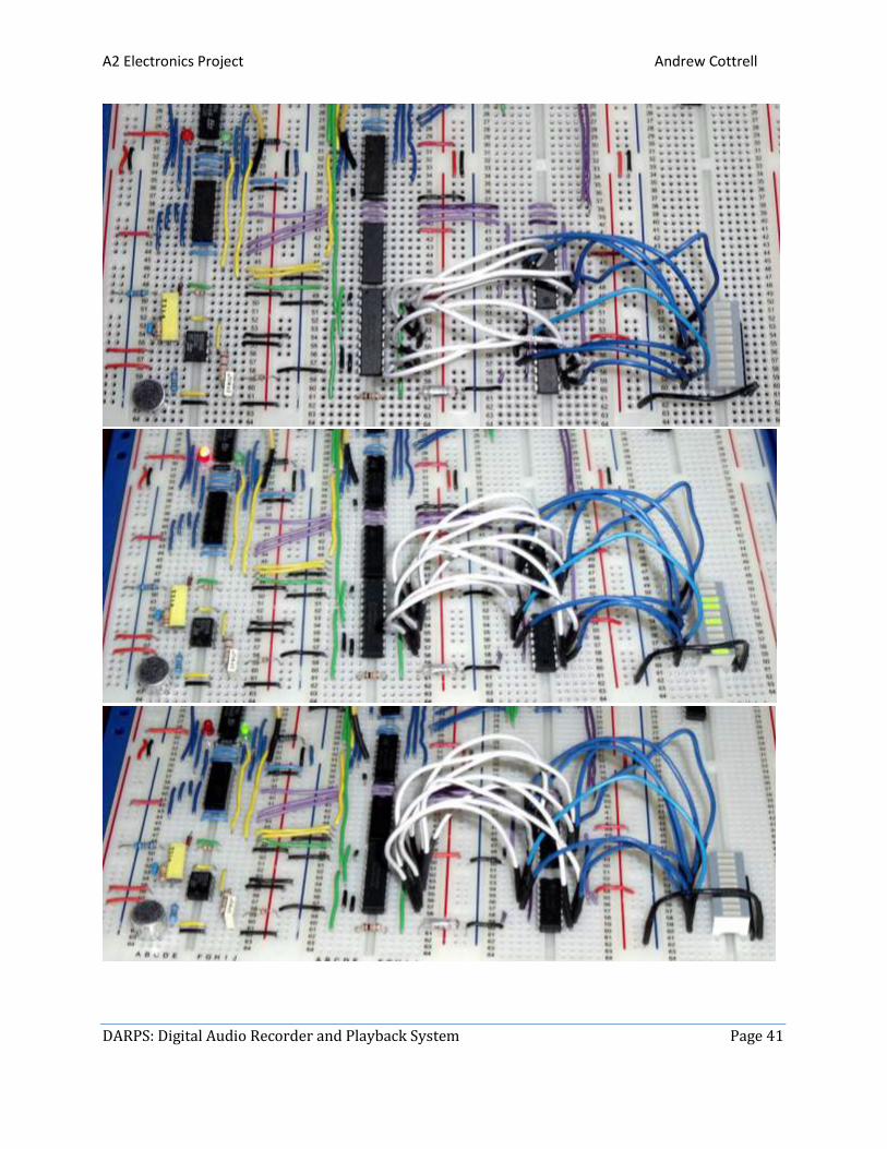
Analogue switches:
Next I connected these lines through the Analogue switches which are
connected to the lines, to make sure that this works effectively.
A2 Electronics Project Andrew Cottrell
DARPS: Digital Audio Recorder and Playback System Page 41
A2 Electronics Project Andrew Cottrell
DARPS: Digital Audio Recorder and Playback System Page 42
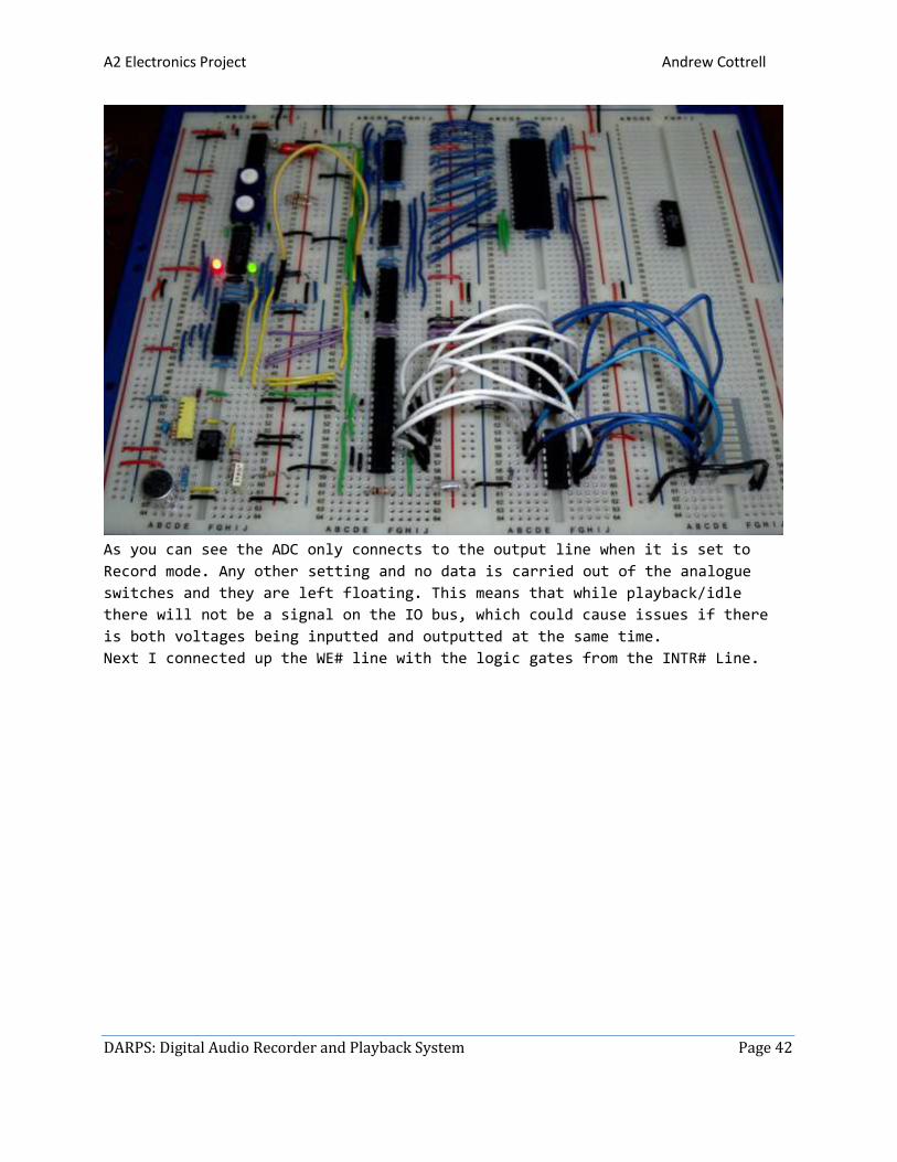
As you can see the ADC only connects to the output line when it is set to
Record mode. Any other setting and no data is carried out of the analogue
switches and they are left floating. This means that while playback/idle
there will not be a signal on the IO bus, which could cause issues if there
is both voltages being inputted and outputted at the same time.
Next I connected up the WE# line with the logic gates from the INTR# Line.

A2 Electronics Project Andrew Cottrell
DARPS: Digital Audio Recorder and Playback System Page 43
As you can see the WE# line is high almost always, apart from the pulse in
between the conversion being ready and the next one starting. This is when
the sample is taken from the ADC and stored into the memory. It is also very
close to 8KHz which is what I wanted.
When any combination other than the only switch being latched is the record,
any other and it is held high.
As you can see here, the pulses time nicely with the change in address.
A2 Electronics Project Andrew Cottrell
DARPS: Digital Audio Recorder and Playback System Page 44
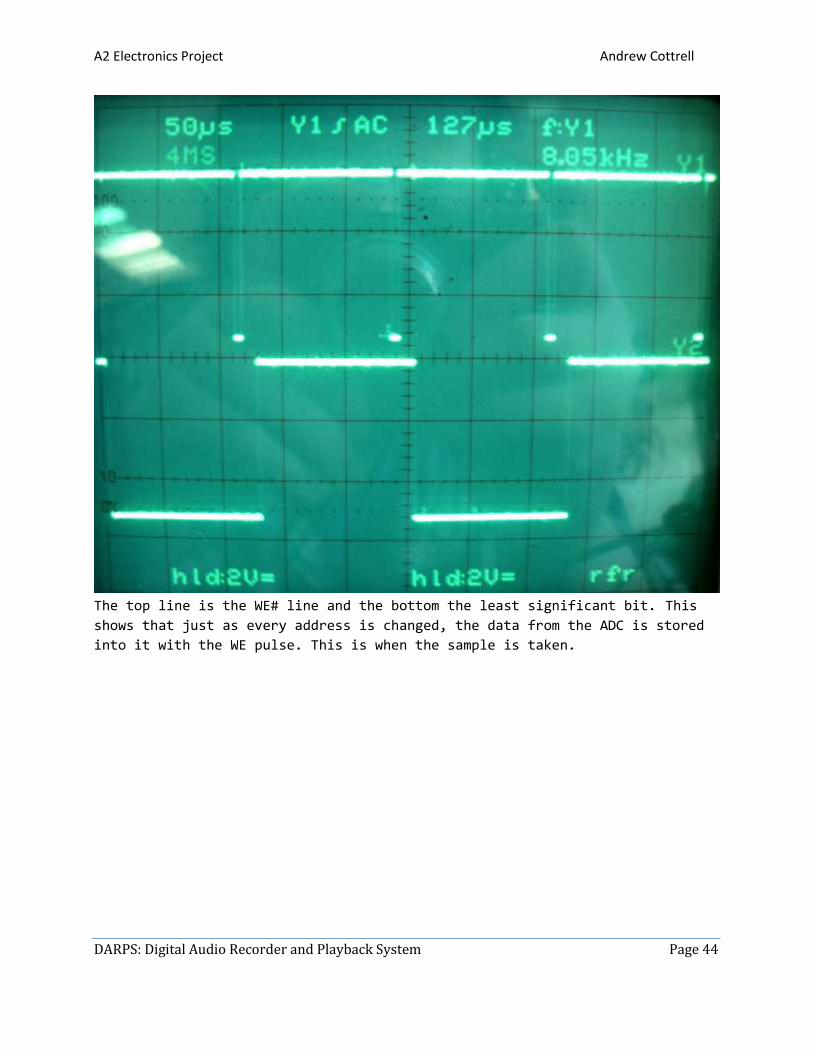
The top line is the WE# line and the bottom the least significant bit. This
shows that just as every address is changed, the data from the ADC is stored
into it with the WE pulse. This is when the sample is taken.
A2 Electronics Project Andrew Cottrell
DARPS: Digital Audio Recorder and Playback System Page 45
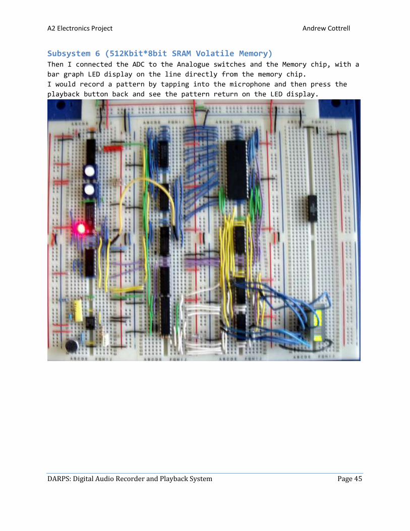
Subsystem 6 (512Kbit*8bit SRAM Volatile Memory) Then I connected the ADC to the Analogue switches and the Memory chip, with a
bar graph LED display on the line directly from the memory chip.
I would record a pattern by tapping into the microphone and then press the
playback button back and see the pattern return on the LED display.

A2 Electronics Project Andrew Cottrell
DARPS: Digital Audio Recorder and Playback System Page 46
In the first picture the LEDs are lighting with the data going in, but in the
second it is coming back from the memory chip. In the same pattern and timing
as it went in.
A2 Electronics Project Andrew Cottrell
DARPS: Digital Audio Recorder and Playback System Page 47
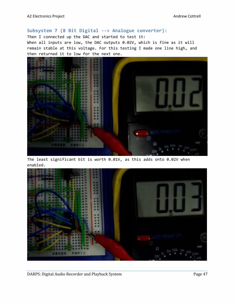
Subsystem 7 (8 Bit Digital --> Analogue converter): Then I connected up the DAC and started to test it:
When all inputs are low, the DAC outputs 0.02V, which is fine as it will
remain stable at this voltage. For this testing I made one line high, and
then returned it to low for the next one.
The least significant bit is worth 0.01V, as this adds onto 0.02V when
enabled.
A2 Electronics Project Andrew Cottrell
DARPS: Digital Audio Recorder and Playback System Page 48
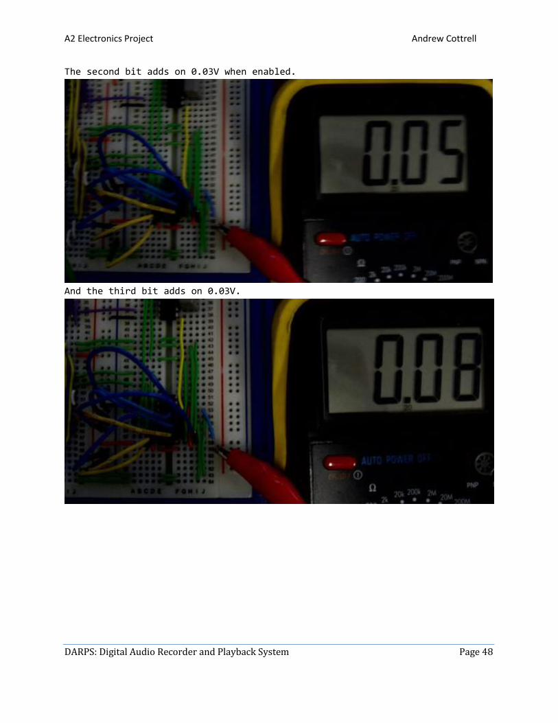
The second bit adds on 0.03V when enabled.
And the third bit adds on 0.03V.

A2 Electronics Project Andrew Cottrell
DARPS: Digital Audio Recorder and Playback System Page 49
The fourth adds on 0.13V.
And then the fifth adds on 0.26V, doubling the fifth as expected.
And then the sixth adds on 0.52V, doubling again.
A2 Electronics Project Andrew Cottrell
DARPS: Digital Audio Recorder and Playback System Page 50
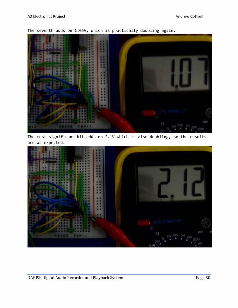
The seventh adds on 1.05V, which is practically doubling again.
The most significant bit adds on 2.1V which is also doubling, so the results
are as expected.
A2 Electronics Project Andrew Cottrell
DARPS: Digital Audio Recorder and Playback System Page 51
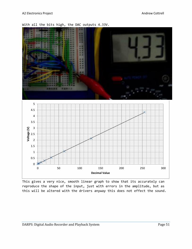
With all the bits high, the DAC outputs 4.33V.
This gives a very nice, smooth linear graph to show that its accurately can
reproduce the shape of the input, just with errors in the amplitude, but as
this will be altered with the drivers anyway this does not effect the sound.
0
0.5
1
1.5
2
2.5
3
3.5
4
4.5
5
0 50 100 150 200 250 300
Vo
ltag
e (
V)
Decimal Value
A2 Electronics Project Andrew Cottrell
DARPS: Digital Audio Recorder and Playback System Page 52
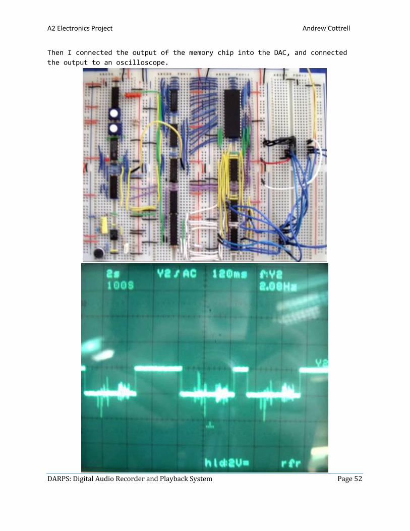
Then I connected the output of the memory chip into the DAC, and connected
the output to an oscilloscope.
A2 Electronics Project Andrew Cottrell
DARPS: Digital Audio Recorder and Playback System Page 53
The first section is the raw data from the ADC going back through the DAC.
The second two are both playbacks from the memory chip. While the waves do
not look perfectly similar, I put this down to the oscilloscope not being
able to show the same points exactly as those peaks were very small in time.
They were taps on the microphone while the later parts are speech.
At this same time I connected a basic pair of headphones to the output and
earth and listened during playback. I could hear what was recorded! However
the signal was very quiet as there was no driver for the audio yet and it was
still running on what the DAC could drive, which was very little.
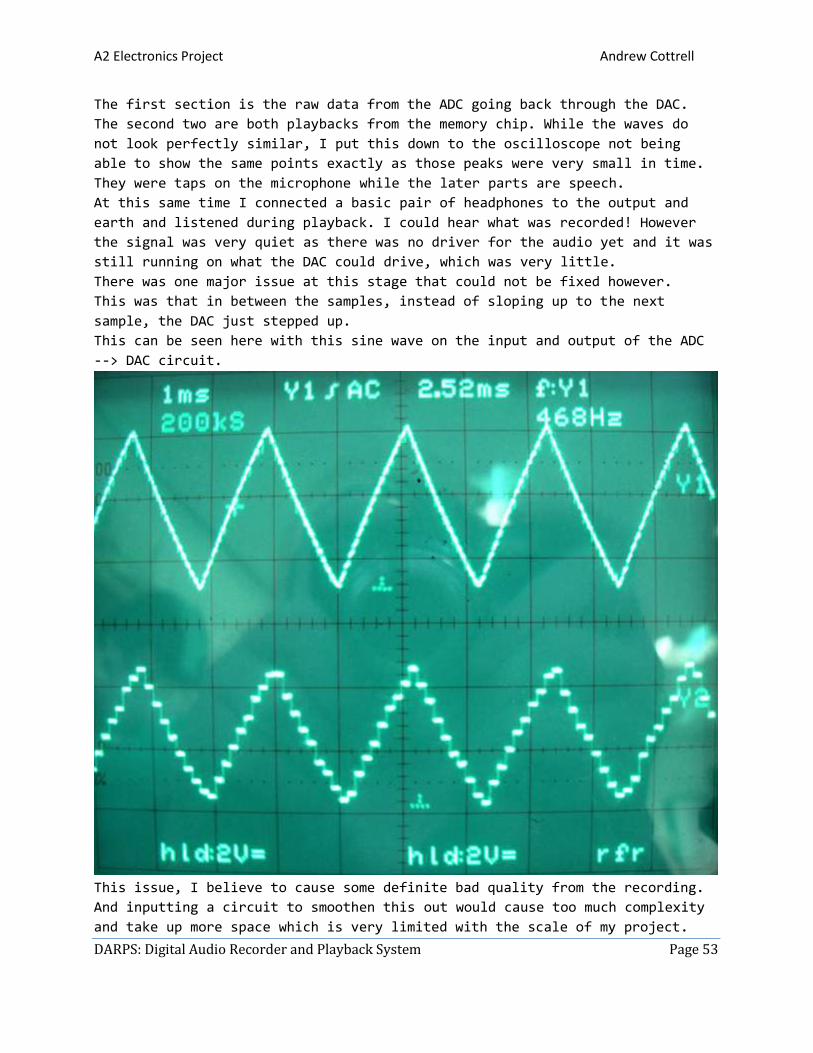
There was one major issue at this stage that could not be fixed however.
This was that in between the samples, instead of sloping up to the next
sample, the DAC just stepped up.
This can be seen here with this sine wave on the input and output of the ADC
--> DAC circuit.
This issue, I believe to cause some definite bad quality from the recording.
And inputting a circuit to smoothen this out would cause too much complexity
and take up more space which is very limited with the scale of my project.
A2 Electronics Project Andrew Cottrell
DARPS: Digital Audio Recorder and Playback System Page 54
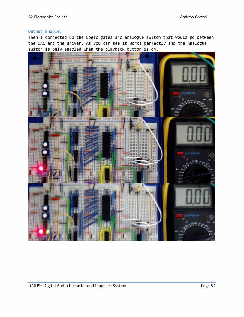
Output Enable:
Then I connected up the Logic gates and analogue switch that would go between
the DAC and the driver. As you can see it works perfectly and the Analogue
switch is only enabled when the playback button is on.
A2 Electronics Project Andrew Cottrell
DARPS: Digital Audio Recorder and Playback System Page 55
Subsystem 8 (Driver and Loudspeaker):
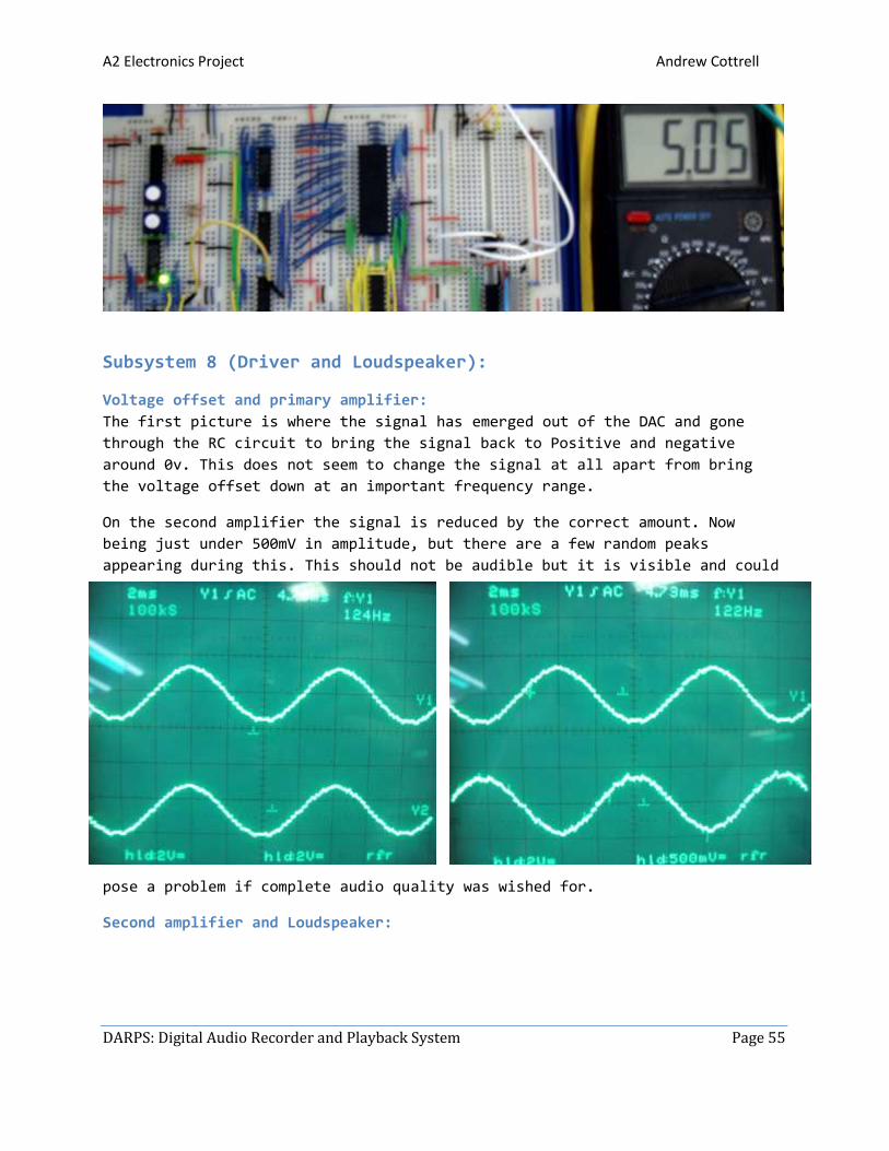
Voltage offset and primary amplifier:
The first picture is where the signal has emerged out of the DAC and gone
through the RC circuit to bring the signal back to Positive and negative
around 0v. This does not seem to change the signal at all apart from bring
the voltage offset down at an important frequency range.
On the second amplifier the signal is reduced by the correct amount. Now
being just under 500mV in amplitude, but there are a few random peaks
appearing during this. This should not be audible but it is visible and could
pose a problem if complete audio quality was wished for.
Second amplifier and Loudspeaker:
A2 Electronics Project Andrew Cottrell
DARPS: Digital Audio Recorder and Playback System Page 56
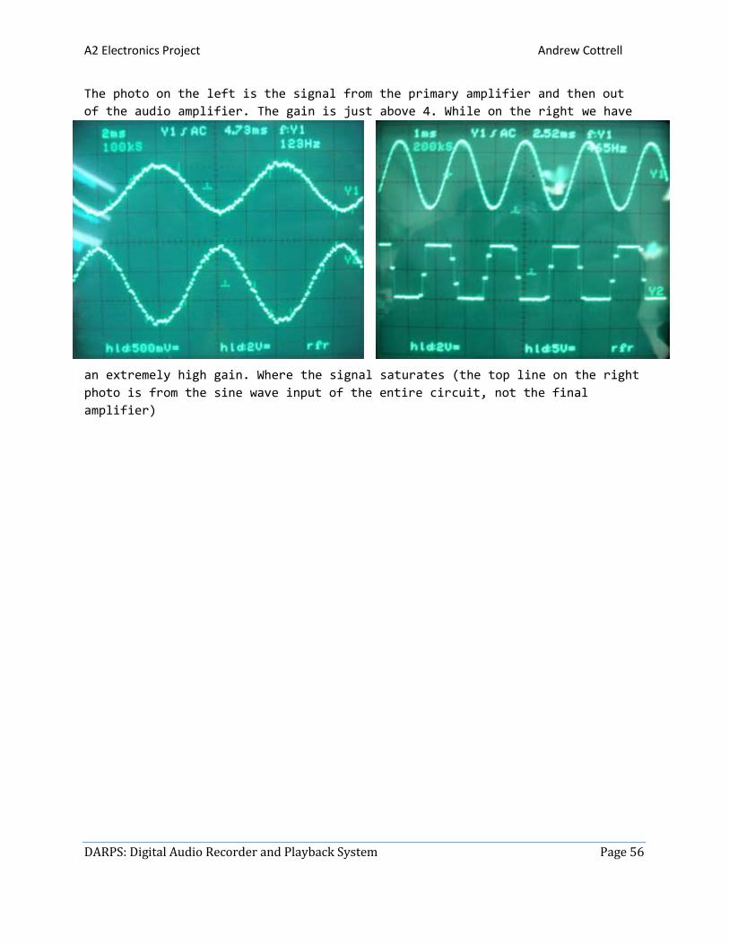
The photo on the left is the signal from the primary amplifier and then out
of the audio amplifier. The gain is just above 4. While on the right we have
an extremely high gain. Where the signal saturates (the top line on the right
photo is from the sine wave input of the entire circuit, not the final
amplifier)
A2 Electronics Project Andrew Cottrell
DARPS: Digital Audio Recorder and Playback System Page 57
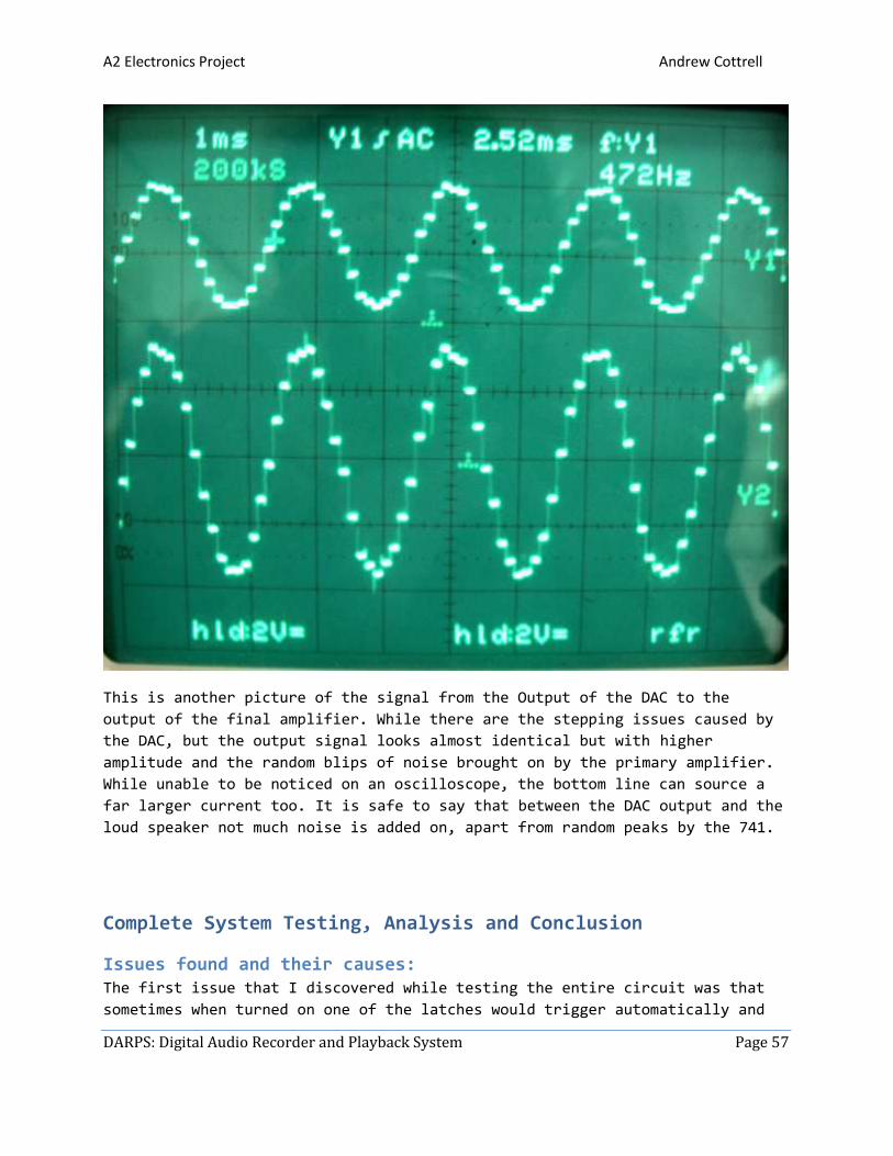
This is another picture of the signal from the Output of the DAC to the
output of the final amplifier. While there are the stepping issues caused by
the DAC, but the output signal looks almost identical but with higher
amplitude and the random blips of noise brought on by the primary amplifier.
While unable to be noticed on an oscilloscope, the bottom line can source a
far larger current too. It is safe to say that between the DAC output and the
loud speaker not much noise is added on, apart from random peaks by the 741.
Complete System Testing, Analysis and Conclusion
Issues found and their causes: The first issue that I discovered while testing the entire circuit was that
sometimes when turned on one of the latches would trigger automatically and

A2 Electronics Project Andrew Cottrell
DARPS: Digital Audio Recorder and Playback System Page 58
start its cycle. Luckily it would self-correct itself by just doing a counter
depending what the counter was set to be. It would always be both LEDs so no
sound would come out of the speaker during this.
Another issue that I discovered was that during recording, a small amount of
what was being recorded would come out of the loud speaker. I put this down
to noise caused by the system while recording which isn’t fully blocked out
by the capacitors and analogue switch.
The third issue that I discovered was that the audio was not very clear and
had a lot of noise. This issue was hard to track down and still could be
multiple possibilities. First, the microphone is not of the best quality and
the quality of the sound can be increased greatly by making sure that the
sound you want to record is at the correct levels otherwise it will either
saturate at the preamp or be overruled by noise.
Another possible cause for this would be that the DAC steps the voltage up,
instead of creating a smooth curve from the samples, just steps voltage up or
down on each sample, this can be seen in the following photographs. In the
first photograph, at a low frequency like 120Hz, this stepping has very
little effect. However, as it gets higher and higher frequency, you can see
it slowly makes more and more effect, and then as it gets to near 1KHz and it
is majorly starting to change it. Any higher and the wave is almost
unrecognisable. While I calculated that 4000Hz should be used to stop
aliasing from the sample rate, this problem causes issues as well that were
not expected. However this is good enough quality to still hear voice clearly
and be able to recognise what song has been stored into it without fixing
such issue.
A2 Electronics Project Andrew Cottrell
DARPS: Digital Audio Recorder and Playback System Page 59
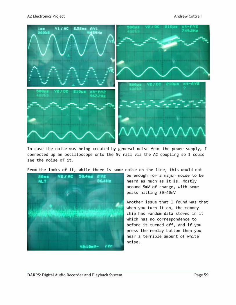
In case the noise was being created by general noise from the power supply, I
connected up an oscilloscope onto the 5v rail via the AC coupling so I could
see the noise of it.
From the looks of it, while there is some noise on the line, this would not
be enough for a major noise to be
heard as much as it is. Mostly
around 5mV of change, with some
peaks hitting 30-40mV
Another issue that I found was that
when you turn it on, the memory
chip has random data stored in it
which has no correspondence to
before it turned off, and if you
press the replay button then you
hear a terrible amount of white
noise.
A2 Electronics Project Andrew Cottrell
DARPS: Digital Audio Recorder and Playback System Page 60
What I would do to fix these issues if I had the resources: A quick fix to the stepping issue would be having an ADC with a much faster
conversion rate. This would allow me to increase the sample rate dramatically
so I could get many samples that the stepping would be near impossible to see
in audible frequencies, this would take a very fast ADC though, which can
cost a lot of money and would take any storage equally fast.
Or instead of this, building a subsystem that would connect up the samples
with a straight line or other suitable voltage increase/decrease between
these values. I believe this could increase the sound quality a lot,
especially when the frequencies are greater than 500Hz
Another upgrade that would be good would be non-volatile memory instead of
volatile which would allow for data to be stored even when the device has
been turned off, and when turned on it would not be full of noise.
Overall conclusion of the project: My project will turn on, record audio and play it back at a decent enough
quality for words to be made out, and music replayed at a fairly enjoyable
level. While there are some definite issues with the system, these do not
majorly effect the way it works or cause issues that cannot be ignored. If a
raw sine wave is put in, then the wave will seem very accurate to the same
wave on the other side, minus the stepping at higher frequencies.
The noise while could be annoying to some is a minimal if recording
conditions are optimum and for use of voice recording will not be an issue.
If you use a media player to sound loud music next to the microphone it comes
out a lot better quality than when you speak into it from a distance.
If the data is injected direly in from a headphone connection on a media
player, ignoring the microphone and preamp the audio quality for the lower
frequencies does increase. However, due to it missing the preamp this does
not get filtered, so perhaps in a future system if both input types were
allowed then the filter and preamp would have to be on a different
amplification system.
The lack of Non-volatile memory can be annoying but if this was made into a
device there are low power modes which some of the chips can be put into and
the only chip that requires power would be the memory chip; so while it being
volatile is not the best, it is easily good enough with easy solutions to
potential problems.
Compared to modern electronics, my circuit is huge. Modern electronics
consisting just of a single microprocessor and possibly some flash memory
A2 Electronics Project Andrew Cottrell
DARPS: Digital Audio Recorder and Playback System Page 61
could do what this circuit does and far more. But those require programming
and are far harder to troubleshoot if something goes wrong. This also has a
far simplified control system.
For the future I would like to add a device which would allow me to pause
recording and then continue from the same spot. Perhaps that would be a clock
enable line. Or a method of stopping recording and then recording a second
two second recording and being able to choose between them.
Another thing that I would like to change is the current method for timing
settings, a jump lead is a very rugged method for switching between these.
Perhaps in the future I would have a dial which could pick between them, or a
3 bit switch digitally connected to a multiplexer to choose between the
settings.
While this system is built for recording audio, it can be used as a data
logger and replay system for any device. As long as you can match up the
input values correctly, so that the input voltage was the correct amount for
the voltage offset or ADC. Then all you need is a little modification to
replace the microphone. Then you could use this to data log temperature, or
anything else that you had an electric probe for. You could also slow down
the clock if you wanted to record this over a long time, and then speed it up
to replay it, perhaps with a potentiometer in the relaxation oscillator to
change the frequency of the clock.
Another thing in the future that I would like to do is to somehow create a
stereo recorder. By adding a second microphone and speaker, and having a
multiplexer switch between each as it records and plays back. However for
this I would need to either double the frequency or put up with half as good
quality. But if I chose to double the frequency I would have to obtain a
better ADC which could go faster than the current on. This would also then
allow me to reach higher frequencies and better quality sound. Perhaps also
then you could have an ADC that could record positive and negative values
from one signal line as well which would remove the need for the initial
voltage offset and make this system simpler.
Finally; I would like to somehow make it run off a power supply so that I
only need 3 voltages, instead of 4. Or perhaps even 2 as having a power
supply unit that would supply all 4 voltages can be difficult to obtain and
can also be expensive, which if for a general consumer would be irritating.
A2 Electronics Project Andrew Cottrell
DARPS: Digital Audio Recorder and Playback System Page 62
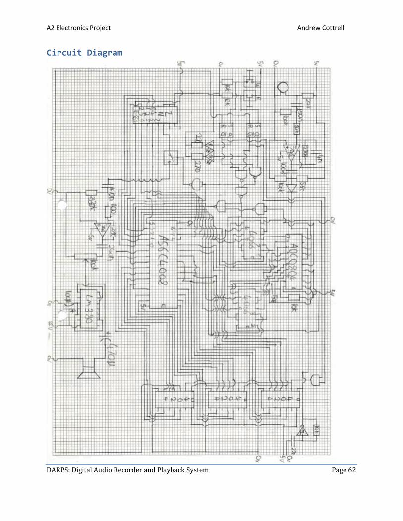
Circuit Diagram
A2 Electronics Project Andrew Cottrell
DARPS: Digital Audio Recorder and Playback System Page 63
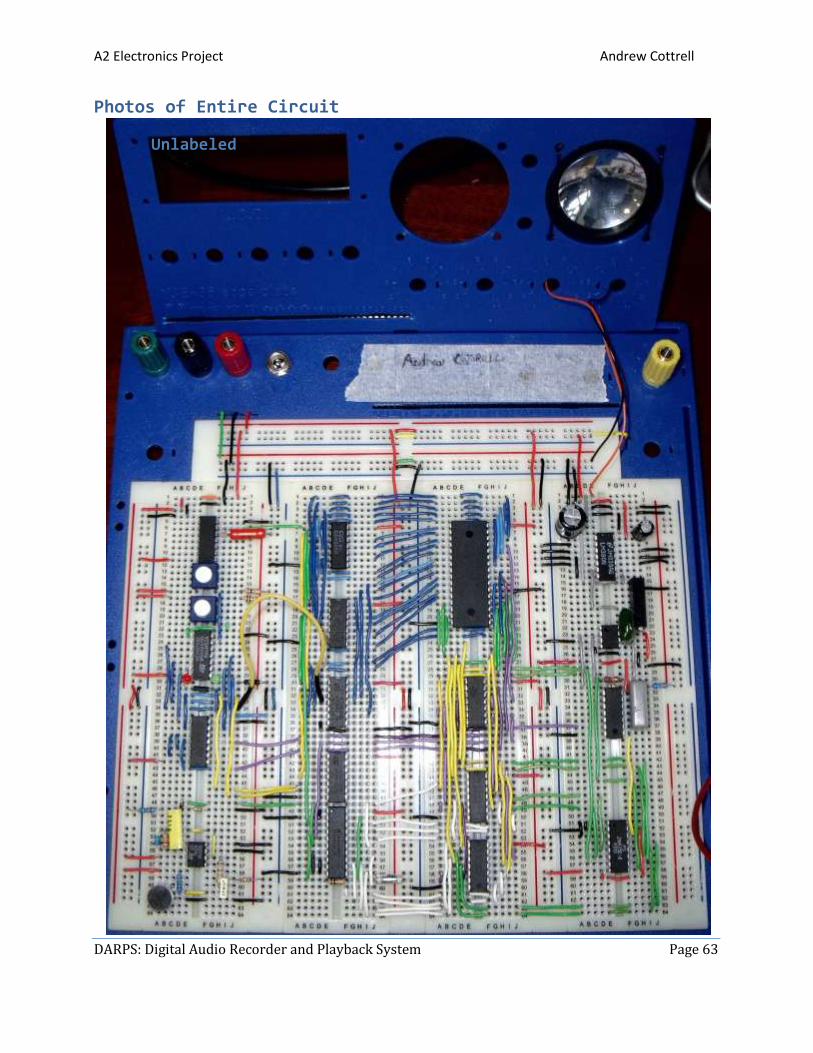
Photos of Entire Circuit
Unlabeled
A2 Electronics Project Andrew Cottrell
DARPS: Digital Audio Recorder and Playback System Page 64
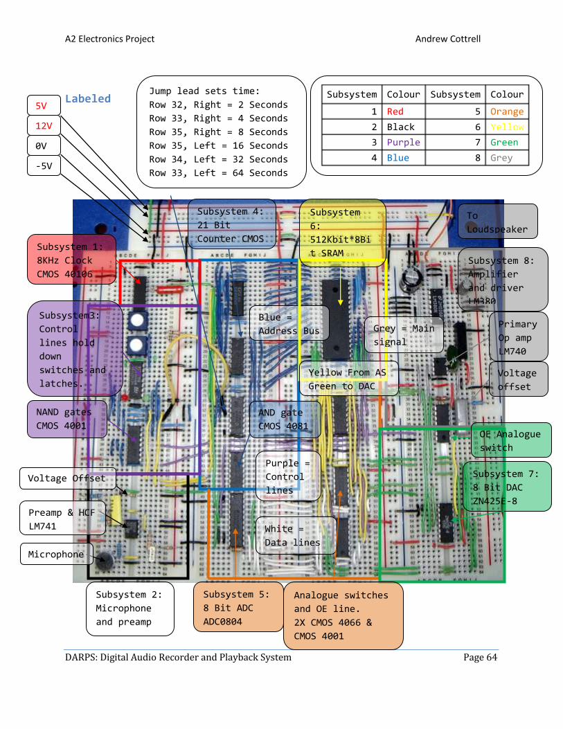
Labeled
Blue =
Address Bus
Yellow From AS
Green to DAC
5V
12V
0V
-5V
Purple =
Control
lines
Subsystem 2:
Microphone
and preamp
White =
Data lines
before AS
Primary
Op amp
LM740
To
Loudspeaker
Preamp & HCF
LM741
Analogue switches
and OE line.
2X CMOS 4066 &
CMOS 4001
Jump lead sets time:
Row 32, Right = 2 Seconds
Row 33, Right = 4 Seconds
Row 35, Right = 8 Seconds
Row 35, Left = 16 Seconds
Row 34, Left = 32 Seconds
Row 33, Left = 64 Seconds
Subsystem Colour Subsystem Colour
1 Red 5 Orange
2 Black 6 Yellow
3 Purple 7 Green
4 Blue 8 Grey
Subsystem 1:
8KHz Clock
CMOS 40106
Subsystem3:
Control
lines hold
down
switches and
latches.
NAND gates
CMOS 4001
Subsystem 4:
21 Bit
Counter CMOS
Subsystem 5:
8 Bit ADC
ADC0804
Subsystem 7:
8 Bit DAC
ZN425E-8
OE Analogue
switch
Voltage
offset
Subsystem
6:
512Kbit*8Bi
t SRAM
Memory
Voltage Offset
Microphone
Grey = Main
signal
AND gate
CMOS 4081
Subsystem 8:
Amplifier
and driver
LM380

A2 Electronics Project Andrew Cottrell
DARPS: Digital Audio Recorder and Playback System Page 65
Full component list Category Specification Quantity
Wire Red 0.896M
Black 1.222M
Purple 0.929M
Yellow 1.199M
Blue 2.363M
Grey 0.23M
Green 1.76M
White 0.802M
Jump 1
Resistors 270Ω 2
10E+3 Ω 5
22E+3 Ω 1
27E+3 Ω 1
56E+3 Ω 1
100E+3 Ω 3
220E+3 Ω 2
Potentiometer 100E+3 Ω 1
Capacitors 240E-9F 1
150E-9F 1
100E-9F 1
47E-9F 1
22E-9F 1
4E-9F 1
150E-12F 1
Electrolytic 470E-6F 1
100E-6F 1
CMOS 4000 Chips 40106 1
4011 2
4013 1
4024 3
4066 3
4081 1
Other Chips LM741 2
LM380 1
ADC0804 1
ZN425E-8 1
AS6C4008 1
Diodes 0.7V Silicon 1
Green Light 1
Red Light 1
Other components Microphone 1
Loudspeaker 1
Push to make Switches 2
Power supply 12V,5V,0V,-5V
A2 Electronics Project Andrew Cottrell
DARPS: Digital Audio Recorder and Playback System Page 66
Bibliography
[1] The useful circuit’s booklet – QMC publication
For the microphone circuit: Page 15. Diagram 1
For the driver circuit: Page 25. Diagram 2.
[2] National Semiconductors ADC0804 Data sheet
(http://www.national.com/ds/DC/ADC0801.pdf)


![[STAFF WORKING DRAFT] - Hackaday€¦ · [STAFF WORKING DRAFT] MARCH 9, 2016 ... Working group on improving air service to small communities. TITLE IV—NEXTGEN AND FAA ORGANIZATION](https://img.pdfslide.net/doc/110x75/605b2adf60e5b02117462996/staff-working-draft-hackaday-staff-working-draft-march-9-2016-working.jpg)