Embed Size (px)
Citation preview
SystemVerilog for Design and Verification
Engineer Explorer Series
Course Version 20.6
Lab Manual Revision 1.0

2 May 11, 2020
© 1990-2020 Cadence Design Systems, Inc. All rights reserved.
Printed in the United States of America.
Cadence Design Systems, Inc. (Cadence), 2655 Seely Ave., San Jose, CA 95134, USA.
Trademarks: Trademarks and service marks of Cadence Design Systems, Inc. (Cadence) contained in this document are
attributed to Cadence with the appropriate symbol. For queries regarding Cadence trademarks, contact the corporate
legal department at the address shown above or call 1-800-862-4522.
All other trademarks are the property of their respective holders.
Restricted Print Permission: This publication is protected by copyright and any unauthorized use of this publication may
violate copyright, trademark, and other laws. Except as specified in this permission statement, this publication may not
be copied, reproduced, modified, published, uploaded, posted, transmitted, or distributed in any way, without prior
written permission from Cadence. This statement grants you permission to print one (1) hard copy of this publication
subject to the following conditions:
The publication may be used solely for personal, informational, and noncommercial purposes;
The publication may not be modified in any way;
Any copy of the publication or portion thereof must include all original copyright, trademark, and other proprietary
notices and this permission statement; and
Cadence reserves the right to revoke this authorization at any time, and any such use shall be discontinued
immediately upon written notice from Cadence.
Disclaimer: Information in this publication is subject to change without notice and does not represent a commitment on
the part of Cadence. The information contained herein is the proprietary and confidential information of Cadence or its
licensors, and is supplied subject to, and may be used only by Cadence customers in accordance with, a written
agreement between Cadence and the customer.
Except as may be explicitly set forth in such agreement, Cadence does not make, and expressly disclaims, any
representations or warranties as to the completeness, accuracy or usefulness of the information contained in this
document. Cadence does not warrant that use of such information will not infringe any third party rights, nor does
Cadence assume any liability for damages or costs of any kind that may result from use of such information.
Restricted Rights: Use, duplication, or disclosure by the Government is subject to restrictions as set forth in
FAR52.227-14 and DFAR252.227-7013 et seq. or its successor.
Cadence Design Systems, Inc. 3
Table of Contents
SystemVerilog for Design and Verification
Overview of Labs .............................................................................................................................. 5 Software Releases ............................................................................................................................. 5
Lab 1 Modeling a Simple Register............................................................................................................ 6 Creating the Register Design ............................................................................................................ 6 Testing the Register Design .............................................................................................................. 7 Run Command .................................................................................................................................. 7
Lab 2 Modeling a Simple Multiplexor (Optional) ................................................................................... 8 Creating the MUX Design ................................................................................................................ 8 Testing the MUX Design .................................................................................................................. 9
Lab 3 Modeling a Simple Counter.......................................................................................................... 10 Creating the Counter Design ........................................................................................................... 11 Testing the Counter Design ............................................................................................................. 11
Lab 4 Modeling a Sequence Controller .................................................................................................. 12 Creating the Controller Design ....................................................................................................... 14 Testing the Controller Design ......................................................................................................... 15
Lab 5 Modeling an Arithmetic Logic Unit (ALU) (Optional) .............................................................. 16 Creating the ALU Design ............................................................................................................... 17 Testing the ALU Design ................................................................................................................. 17
Lab 6 Testing a Memory Module ........................................................................................................... 18 Completing the Memory Testbench ................................................................................................ 19 Testing the Memory ........................................................................................................................ 20
Lab 7 Using a Memory Interface ............................................................................................................ 21 Adding the Memory Interface ......................................................................................................... 21
Lab 8 Verifying the VeriRISC CPU (Optional) .................................................................................... 23 Assembling the CPU Model............................................................................................................ 24 Reviewing the CPU Testbench ....................................................................................................... 25 CPU Diagnostic Programs .............................................................................................................. 25 Testing the CPU .............................................................................................................................. 26
Lab 9 Using a Simple Clocking Block .................................................................................................... 27 Creating the Clocking Block ........................................................................................................... 27
Lab 10 Using Scope-Based Randomization ............................................................................................. 28 Modifying the Memory Testbench .................................................................................................. 28
Lab 11 Using Classes ................................................................................................................................. 29 Creating a Simple Class .................................................................................................................. 29 Adding a Class Constructor ............................................................................................................ 30 Defining Derived Classes ................................................................................................................ 30 Setting Counter Limits .................................................................................................................... 31 Indicating Roll-Over and Roll-Under ............................................................................................. 32 Implementing a Static Property and a Static Method ...................................................................... 32 Defining an Aggregate Class .......................................................................................................... 33
Lab 12 Using Class Polymorphism and Virtual Methods ...................................................................... 34
Lab 13 Using Class-Based Randomization .............................................................................................. 35 Adding Class-Based Randomization ............................................................................................... 35
4 Cadence Design Systems, Inc.
Lab 14 Using Virtual Interfaces................................................................................................................ 37 Adding a Virtual Interface............................................................................................................... 37 Using a Virtual Interface with Multiple Memories (Optional) ........................................................ 38
Lab 15 Simple Covergroup Coverage ...................................................................................................... 39 Adding a Covergroup and Capturing Coverage .............................................................................. 39 Analyzing Coverage ........................................................................................................................ 40
Lab 16 Analyzing Cross Coverage (Optional) ......................................................................................... 42 Creating the ALU Coverage Model ................................................................................................ 43
Lab 17 Using Dynamic Arrays and Queues ............................................................................................. 44 Adding a Dynamic Array Scoreboard ............................................................................................. 44 Adding an Associative Array Scoreboard ....................................................................................... 44 Adding a Queue Scoreboard ........................................................................................................... 45
Lab 18 Simulating Simple Implication Assertions .................................................................................. 46 Creating the Assertions ................................................................................................................... 47 Simulating Your Assertions ............................................................................................................ 47 Modifying the Assertions ................................................................................................................ 48 Conclusions ..................................................................................................................................... 48
Lab 19 Sequence-Based Properties ........................................................................................................... 49 Creating the Simple Sequence Assertion ........................................................................................ 50 Creating the Complex Sequence Assertion ..................................................................................... 51 Answers to Questions ...................................................................................................................... 52
Lab 20 Simple DPI Use .............................................................................................................................. 53
Lab 21 Synchronizing Processes with a Mailbox .................................................................................... 54 Examining the Mailbox Test Case .................................................................................................. 54 Completing and Simulating the Mailbox Test Case ........................................................................ 55
Lab 22 Synchronizing Processes with a Semaphore ............................................................................... 56 Completing and Simulating the Semaphore Test Case ................................................................... 56
Lab 23 Synchronizing Processes with Events (Optional) ....................................................................... 57 Resolving an Undefined Process Execution Order (Race) Condition ............................................. 57
Overview of Labs
© 2020 Cadence Design Systems, Inc. All rights reserved. 5
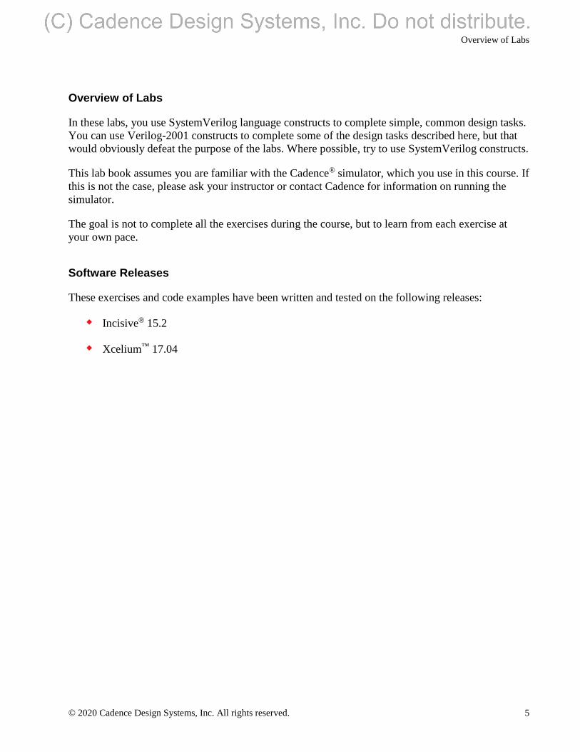
Overview of Labs
In these labs, you use SystemVerilog language constructs to complete simple, common design tasks.
You can use Verilog-2001 constructs to complete some of the design tasks described here, but that
would obviously defeat the purpose of the labs. Where possible, try to use SystemVerilog constructs.
This lab book assumes you are familiar with the Cadence® simulator, which you use in this course. If
this is not the case, please ask your instructor or contact Cadence for information on running the
simulator.
The goal is not to complete all the exercises during the course, but to learn from each exercise at
your own pace.
Software Releases
These exercises and code examples have been written and tested on the following releases:
Incisive® 15.2
Xcelium™ 17.04
Modeling a Simple Register
6 © 2020 Cadence Design Systems, Inc. All rights reserved.
Lab 1 Modeling a Simple Register
Objective: To use SystemVerilog procedural constructs to model a simple register.
Create a simple register design using SystemVerilog and Verilog-2001 constructs and test it using
the supplied testbench.
Read the specification first and then follow the instructions in the Creating the Register Design
section.
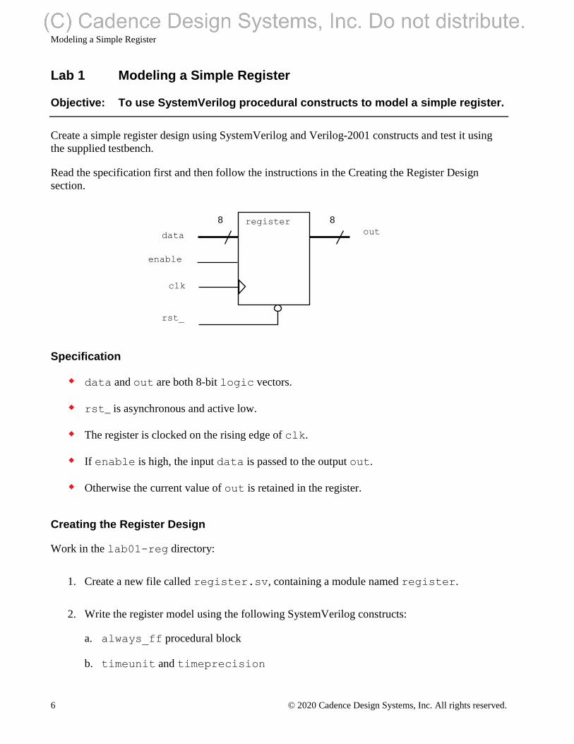
Specification
data and out are both 8-bit logic vectors.
rst_ is asynchronous and active low.
The register is clocked on the rising edge of clk.
If enable is high, the input data is passed to the output out.
Otherwise the current value of out is retained in the register.
Creating the Register Design
Work in the lab01-reg directory:
1. Create a new file called register.sv, containing a module named register.
2. Write the register model using the following SystemVerilog constructs:
a. always_ff procedural block
b. timeunit and timeprecision
8
data
enable
clk
rst_
out
register 8
Modeling a Simple Register
© 2020 Cadence Design Systems, Inc. All rights reserved. 7
c. Verilog2001 ANSI-C port declarations
Testing the Register Design
3. A testbench is provided in the file register_test.sv. Simulate the testbench
and register design.
You should see the following results:
time= 0.0 ns enable=x rst_=1 data=xx out=xx
time= 15.0 ns enable=x rst_=0 data=xx out=00
time= 25.0 ns enable=0 rst_=1 data=xx out=00
time= 35.0 ns enable=1 rst_=1 data=aa out=aa
time= 45.0 ns enable=0 rst_=1 data=55 out=aa
time= 55.0 ns enable=x rst_=0 data=xx out=00
time= 65.0 ns enable=0 rst_=1 data=xx out=00
time= 75.0 ns enable=1 rst_=1 data=55 out=55
time= 85.0 ns enable=0 rst_=1 data=aa out=55
REGISTER TEST PASSED
Debug your register as required.
4. When the test passes, copy the register.sv file into the ../sv_src directory.
You will use it later for the complete VeriRISC design lab.
Run Command
xrun register.sv register_test.sv ( Batch Mode)
xrun register.sv register_test.sv -gui -access +rwc ( GUI Mode)
Modeling a Simple Multiplexor
8 © 2020 Cadence Design Systems, Inc. All rights reserved.
Lab 2 Modeling a Simple Multiplexor (Optional)
Objective: To use SystemVerilog procedural constructs to model a simple multiplexor.
Create a simple multiplexor design using SystemVerilog and Verilog-2001 constructs and test it
using the supplied testbench.
Read the specification first and then follow the instructions in Creating the MUX Design.
Specification
in_a, in_b and out are all logic vectors.
The MUX width is parameterized with a default value of 1.
If sel_a is 1’b1, input in_a is passed to the output.
If sel_a is 1’b0, input in_b is passed to the output.
Creating the MUX Design
Work in the lab02-mux directory:
1. Create a new file called scale_mux.sv, containing a module named scale_mux.
2. Write the MUX model using the following SystemVerilog and Verilog constructs:
▪ Verilog2001 ANSI-C port declarations
Parameterize the MUX width and give it a default value of 1
▪ always_comb procedural block
▪ timeunit and timeprecision
in_a
in_b
sel_a
out mux
Modeling a Simple Multiplexor
© 2020 Cadence Design Systems, Inc. All rights reserved. 9
▪ unique case construct
Include a default match that sets the output to unknown
Testing the MUX Design
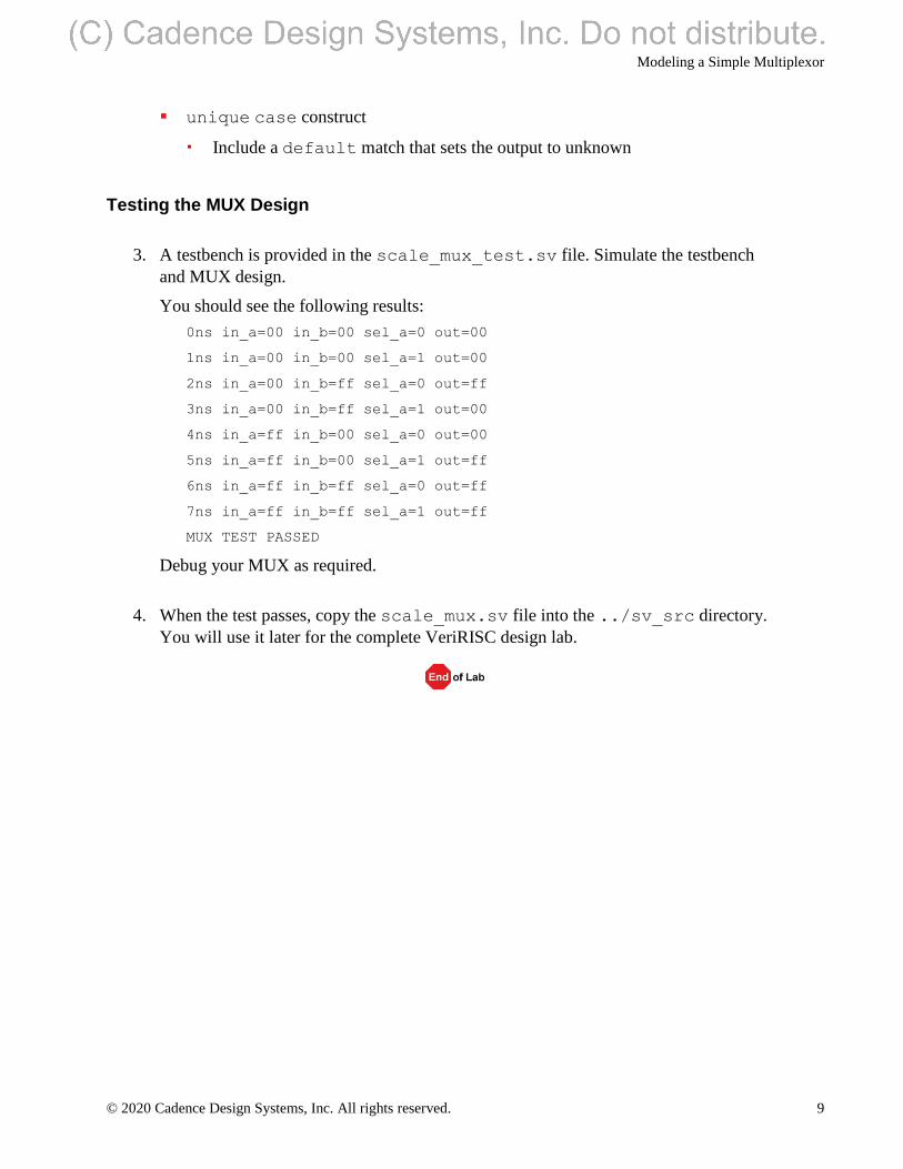
3. A testbench is provided in the scale_mux_test.sv file. Simulate the testbench
and MUX design.
You should see the following results:
0ns in_a=00 in_b=00 sel_a=0 out=00
1ns in_a=00 in_b=00 sel_a=1 out=00
2ns in_a=00 in_b=ff sel_a=0 out=ff
3ns in_a=00 in_b=ff sel_a=1 out=00
4ns in_a=ff in_b=00 sel_a=0 out=00
5ns in_a=ff in_b=00 sel_a=1 out=ff
6ns in_a=ff in_b=ff sel_a=0 out=ff
7ns in_a=ff in_b=ff sel_a=1 out=ff
MUX TEST PASSED
Debug your MUX as required.
4. When the test passes, copy the scale_mux.sv file into the ../sv_src directory.
You will use it later for the complete VeriRISC design lab.
Modeling a Simple Counter
10 © 2020 Cadence Design Systems, Inc. All rights reserved.
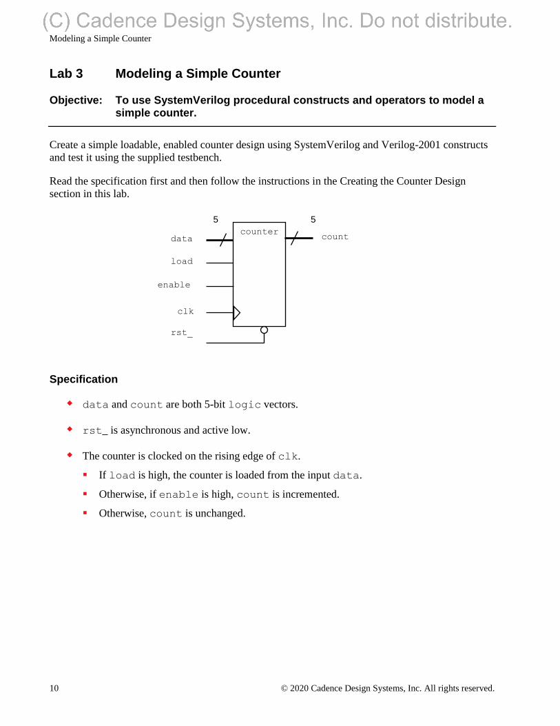
Lab 3 Modeling a Simple Counter
Objective: To use SystemVerilog procedural constructs and operators to model a simple counter.
Create a simple loadable, enabled counter design using SystemVerilog and Verilog-2001 constructs
and test it using the supplied testbench.
Read the specification first and then follow the instructions in the Creating the Counter Design
section in this lab.
Specification
data and count are both 5-bit logic vectors.
rst_ is asynchronous and active low.
The counter is clocked on the rising edge of clk.
▪ If load is high, the counter is loaded from the input data.
▪ Otherwise, if enable is high, count is incremented.
▪ Otherwise, count is unchanged.
data
load
clk
rst_
count counter
5 5
enable
Modeling a Simple Counter
© 2020 Cadence Design Systems, Inc. All rights reserved. 11
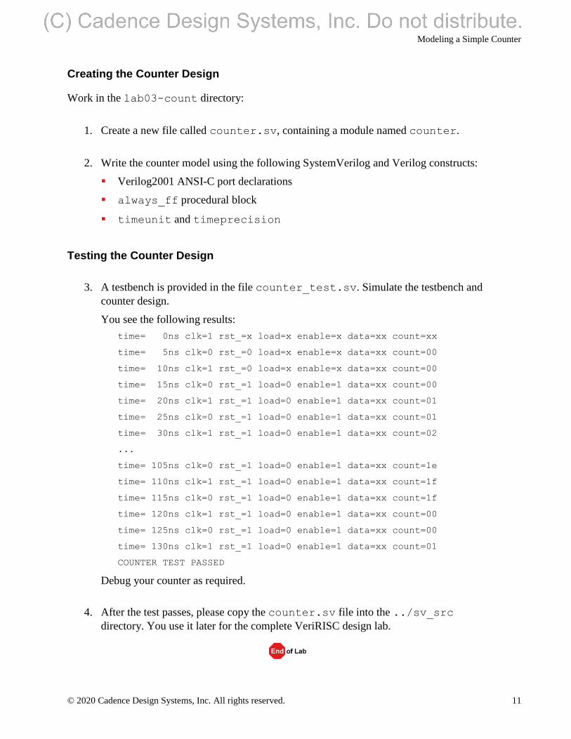
Creating the Counter Design
Work in the lab03-count directory:
1. Create a new file called counter.sv, containing a module named counter.
2. Write the counter model using the following SystemVerilog and Verilog constructs:
▪ Verilog2001 ANSI-C port declarations
▪ always_ff procedural block
▪ timeunit and timeprecision
Testing the Counter Design
3. A testbench is provided in the file counter_test.sv. Simulate the testbench and
counter design.
You see the following results:
time= 0ns clk=1 rst_=x load=x enable=x data=xx count=xx
time= 5ns clk=0 rst_=0 load=x enable=x data=xx count=00
time= 10ns clk=1 rst_=0 load=x enable=x data=xx count=00
time= 15ns clk=0 rst_=1 load=0 enable=1 data=xx count=00
time= 20ns clk=1 rst_=1 load=0 enable=1 data=xx count=01
time= 25ns clk=0 rst_=1 load=0 enable=1 data=xx count=01
time= 30ns clk=1 rst_=1 load=0 enable=1 data=xx count=02
...
time= 105ns clk=0 rst_=1 load=0 enable=1 data=xx count=1e
time= 110ns clk=1 rst_=1 load=0 enable=1 data=xx count=1f
time= 115ns clk=0 rst_=1 load=0 enable=1 data=xx count=1f
time= 120ns clk=1 rst_=1 load=0 enable=1 data=xx count=00
time= 125ns clk=0 rst_=1 load=0 enable=1 data=xx count=00
time= 130ns clk=1 rst_=1 load=0 enable=1 data=xx count=01
COUNTER TEST PASSED
Debug your counter as required.
4. After the test passes, please copy the counter.sv file into the ../sv_src
directory. You use it later for the complete VeriRISC design lab.
Modeling a Sequence Controller
12 © 2020 Cadence Design Systems, Inc. All rights reserved.
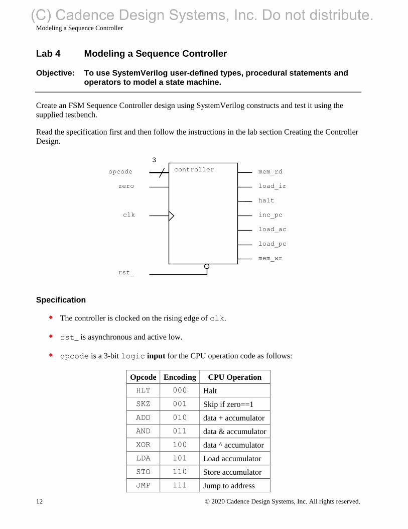
Lab 4 Modeling a Sequence Controller
Objective: To use SystemVerilog user-defined types, procedural statements and operators to model a state machine.
Create an FSM Sequence Controller design using SystemVerilog constructs and test it using the
supplied testbench.
Read the specification first and then follow the instructions in the lab section Creating the Controller
Design.
Specification
The controller is clocked on the rising edge of clk.
rst_ is asynchronous and active low.
opcode is a 3-bit logic input for the CPU operation code as follows:
Opcode Encoding CPU Operation
HLT 000 Halt
SKZ 001 Skip if zero==1
ADD 010 data + accumulator
AND 011 data & accumulator
XOR 100 data ^ accumulator
LDA 101 Load accumulator
STO 110 Store accumulator
JMP 111 Jump to address
opcode
zero
clk
rst_
controller mem_rd
load_ir
halt
inc_pc
load_ac
load_pc
mem_wr
3
Modeling a Sequence Controller
© 2020 Cadence Design Systems, Inc. All rights reserved. 13
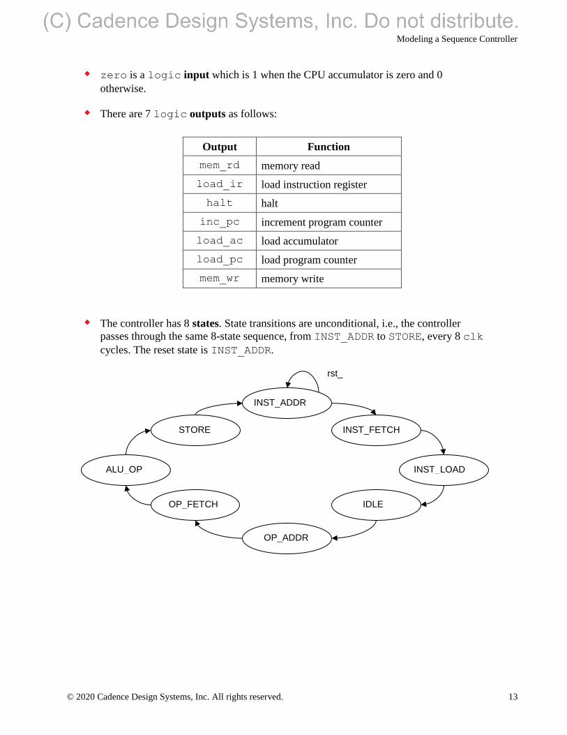
zero is a logic input which is 1 when the CPU accumulator is zero and 0
otherwise.
There are 7 logic outputs as follows:
Output Function
mem_rd memory read
load_ir load instruction register
halt halt
inc_pc increment program counter
load_ac load accumulator
load_pc load program counter
mem_wr memory write
The controller has 8 states. State transitions are unconditional, i.e., the controller
passes through the same 8-state sequence, from INST_ADDR to STORE, every 8 clk
cycles. The reset state is INST_ADDR.
INST_FETCH
INST_ADDR
INST_LOAD
IDLE
OP_ADDR
OP_FETCH
ALU_OP
STORE
rst_
Modeling a Sequence Controller
14 © 2020 Cadence Design Systems, Inc. All rights reserved.
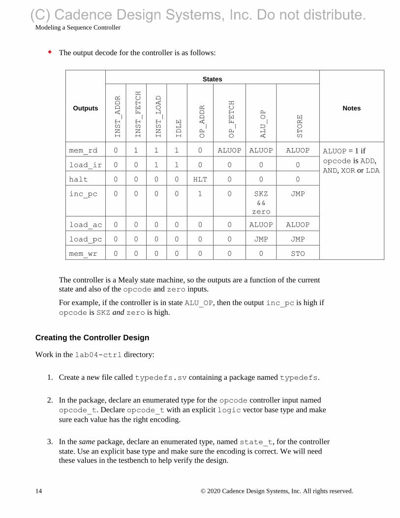
The output decode for the controller is as follows:
Outputs
States
Notes
INST_ADDR
INST_FETCH
INST_LOAD
IDLE
OP_ADDR
OP_FETCH
ALU_OP
STORE
mem_rd 0 1 1 1 0 ALUOP ALUOP ALUOP ALUOP = 1 if
opcode is ADD,
AND, XOR or LDA
load_ir 0 0 1 1 0 0 0 0
halt 0 0 0 0 HLT 0 0 0
inc_pc 0 0 0 0 1 0 SKZ
&&
zero
JMP
load_ac 0 0 0 0 0 0 ALUOP ALUOP
load_pc 0 0 0 0 0 0 JMP JMP
mem_wr 0 0 0 0 0 0 0 STO
The controller is a Mealy state machine, so the outputs are a function of the current
state and also of the opcode and zero inputs.
For example, if the controller is in state ALU_OP, then the output inc_pc is high if
opcode is SKZ and zero is high.
Creating the Controller Design
Work in the lab04-ctrl directory:
1. Create a new file called typedefs.sv containing a package named typedefs.
2. In the package, declare an enumerated type for the opcode controller input named
opcode_t. Declare opcode_t with an explicit logic vector base type and make
sure each value has the right encoding.
3. In the same package, declare an enumerated type, named state_t, for the controller
state. Use an explicit base type and make sure the encoding is correct. We will need
these values in the testbench to help verify the design.
Modeling a Sequence Controller
© 2020 Cadence Design Systems, Inc. All rights reserved. 15
4. Complete the controller definition in the file control.sv using SystemVerilog
constructs where possible:
a. Import the package and use your enumerated type declarations for the input
opcode and state variable(s) of the controller input.
b. Complete the state generation procedure using enumeration methods.
c. Generate outputs based on the current phase using the table above. Use
always_comb and either unique case or unique if constructs. Be sure
to include a default match in the case statement.
Testing the Controller Design
5. Check that your package containing the enumerated type declarations is imported into
control_test.sv. If you did not name your enumerated types opcode_t and
state_t, then you will need to modify the testbench to use your own type names.
6. Simulate the testbench and controller design. Make sure you compile your package
file before compiling any modules which import the package. You do not need to
compile the *.pat files – these are read by the testbench.
If there is a problem with your design, then you should see something similar to the
following output:
CONTROLLER TEST FAILED
{mem_rd,load_ir,halt,inc_pc,load_ac,load_pc,mem_wr}
is 0000000
should be 1000000
state: INST_FETCH opcode: HLT zero: 0
This tells you that the mem_rd output is 0 when it should be 1 in state
INST_FETCH when the opcode input is HLT and zero input is 0.
Debug your controller as required, until you see the message:
CONTROLLER TEST PASSED
7. After the test passes, please copy the control.sv file into the ../sv_src
directory. You will use it later for the complete VeriRISC design lab.
Modeling an Arithmetic Logic Unit
16 © 2020 Cadence Design Systems, Inc. All rights reserved.
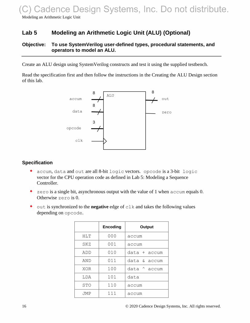
Lab 5 Modeling an Arithmetic Logic Unit (ALU) (Optional)
Objective: To use SystemVerilog user-defined types, procedural statements, and operators to model an ALU.
Create an ALU design using SystemVerilog constructs and test it using the supplied testbench.
Read the specification first and then follow the instructions in the Creating the ALU Design section
of this lab.
Specification
accum, data and out are all 8-bit logic vectors. opcode is a 3-bit logic
vector for the CPU operation code as defined in Lab 5: Modeling a Sequence
Controller.
zero is a single bit, asynchronous output with the value of 1 when accum equals 0.
Otherwise zero is 0.
out is synchronized to the negative edge of clk and takes the following values
depending on opcode.
Encoding Output
HLT 000 accum
SKZ 001 accum
ADD 010 data + accum
AND 011 data & accum
XOR 100 data ^ accum
LDA 101 data
STO 110 accum
JMP 111 accum
accum
clk
ALU out
zero
8 8
data
8
opcode
3
Modeling an Arithmetic Logic Unit
© 2020 Cadence Design Systems, Inc. All rights reserved. 17
Creating the ALU Design
Work in the lab05-alu directory:
1. Copy your typedefs.sv package, containing the opcode type declaration, from
the Controller lab.
2. Create a new file called alu.sv, containing a module named alu.
3. Write the ALU model using the following SystemVerilog and Verilog constructs:
▪ import for the package
▪ Verilog2001 ANSI-C port declarations
▪ timeunit and timeprecision
▪ always_comb procedural block to generate zero
▪ always_ff procedural block to generate out
Testing the ALU Design
4. Check that your package containing the opcode type declarations is imported into
alu_test.sv.
5. Simulate the testbench and controller design.
Debug your ALU as required, until you see the following message:
ALU TEST PASSED
6. After the test passes, copy the alu.sv file into the ../sv_src directory. You use
it later for the complete VeriRISC design lab.
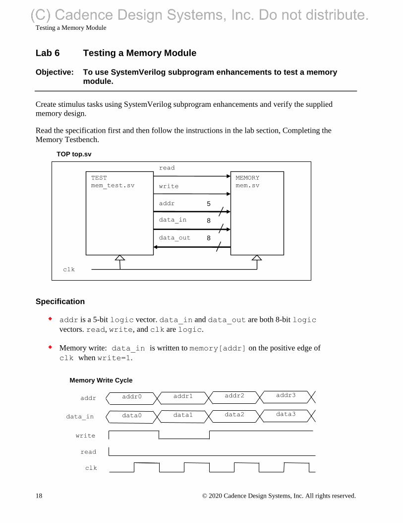
Testing a Memory Module
18 © 2020 Cadence Design Systems, Inc. All rights reserved.
Lab 6 Testing a Memory Module
Objective: To use SystemVerilog subprogram enhancements to test a memory module.
Create stimulus tasks using SystemVerilog subprogram enhancements and verify the supplied
memory design.
Read the specification first and then follow the instructions in the lab section, Completing the
Memory Testbench.
Specification
addr is a 5-bit logic vector. data_in and data_out are both 8-bit logic
vectors. read, write, and clk are logic.
Memory write: data_in is written to memory[addr] on the positive edge of
clk when write=1.
TEST
mem_test.sv
MEMORY
mem.sv
5
8
8 data_out
data_in
write
read
addr
clk
TOP top.sv
addr addr1 addr0 addr2 addr3
data1 data0 data2 data3 data_in
write
clk
read
Memory Write Cycle
Testing a Memory Module
© 2020 Cadence Design Systems, Inc. All rights reserved. 19
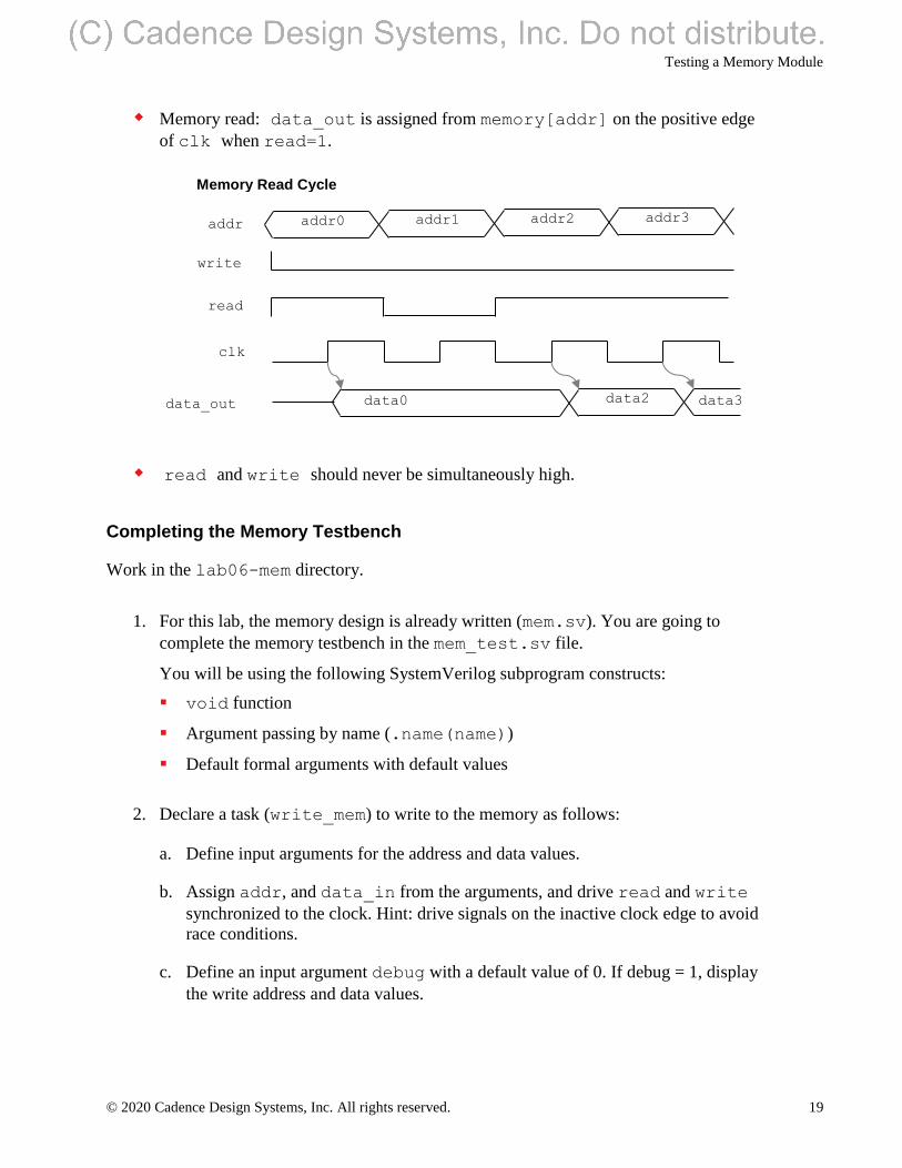
Memory read: data_out is assigned from memory[addr] on the positive edge
of clk when read=1.
read and write should never be simultaneously high.
Completing the Memory Testbench
Work in the lab06-mem directory.
1. For this lab, the memory design is already written (mem.sv). You are going to
complete the memory testbench in the mem_test.sv file.
You will be using the following SystemVerilog subprogram constructs:
▪ void function
▪ Argument passing by name (.name(name))
▪ Default formal arguments with default values
2. Declare a task (write_mem) to write to the memory as follows:
a. Define input arguments for the address and data values.
b. Assign addr, and data_in from the arguments, and drive read and write
synchronized to the clock. Hint: drive signals on the inactive clock edge to avoid
race conditions.
c. Define an input argument debug with a default value of 0. If debug = 1, display
the write address and data values.
addr addr1 addr0 addr2 addr3
data0 data2 data_out
write
clk
read
Memory Read Cycle
data3
Testing a Memory Module
20 © 2020 Cadence Design Systems, Inc. All rights reserved.
3. Declare a task (read_mem) to read the memory as follows:
a. Define an input argument for the address value and output argument for the read
data. Remember to use blocking assignment for assigning read data to output
argument, so that assignment is complete upon return to caller.
b. Assign addr from the argument, and drive read and write, synchronized to
the clock. Hint: drive signals on the inactive clock edge to avoid race conditions.
c. Assign the output data argument from data_out at an appropriate time. There is
a short propagation delay between the rising edge of clk and data_out
updating.
d. Input argument debug with a default value of 0. If debug = 1, display the read
address and data values.
4. Complete the “Clearing the Memory” test by writing zero to every address location,
and then reading back and checking the data read matches the data written.
5. Complete the “Data = Address” test by writing data equal to the address to every
address location, and then reading back and checking the data read matches the data
written.
6. Write a void function (printstatus) with an input argument status which
indicates the number of errors encountered in the tests. If status = 0, the test
passed.
Testing the Memory
7. Simulate the testbench and memory design.
Remember to compile also the top.sv module which instantiates and connects both
design and testbench.
Debug your subprograms as required, until you are happy the design is verified.
Using a Memory Interface
© 2020 Cadence Design Systems, Inc. All rights reserved. 21
Lab 7 Using a Memory Interface
Objective: To use a SystemVerilog interface with ports, modports and methods.
Modify the Memory testbench and design to connect via a SystemVerilog interface.
Adding the Memory Interface
Work in the lab07-intf directory:
1. Copy your Memory design (mem.sv), testbench (mem_test.sv) and top-level
module (top.sv) from lab06-mem into lab07-intf.
2. Define the Memory interface in a new file and declarations for the addr, data_in,
data_out, read and write signals.
3. Edit your Memory design and testbench by updating the port list with an interface
port and referencing the interface signals via the interface port name.
4. Modify the top-level module to make an instantiation of the interface and connect this
to the Memory design and testbench instances.
5. Rerun your memory test to check that the interface is working correctly.
6. Add a clock input port to your interface. Remove the clock ports from your Memory
design and testbench modules. Update your interface instance to map the clk signal
to the clock port. Rerun your memory test to check the interface port is working
correctly.
7. Add modports to the interface to define directional information for both the design
and testbench. Reference the modports in your design and testbench port list. Rerun
your memory test to check that the modports work correctly.
Using a Memory Interface
22 © 2020 Cadence Design Systems, Inc. All rights reserved.
8. Redefine the write_mem() and read_mem() tasks as interface methods:
a. Move the task declarations into the interface.
b. Update the testbench to reference the tasks via the interface.
c. Update your testbench modport to allow access to the interface methods via an
import statement.
d. Rerun your memory test.
Verifying the VeriRISC CPU
© 2020 Cadence Design Systems, Inc. All rights reserved. 23
Lab 8 Verifying the VeriRISC CPU (Optional)
Objective: To assemble and test the VeriRISC CPU model.
Assemble the blocks of the CPU using SystemVerilog connectivity enhancements, and test the
design using the supplied testbench and diagnostic programs.
You can do this lab exercise any time after Lab 6.
Read the specification first and then follow the instructions in the lab section, Assembling the CPU
Model.
controller
halt
load_ac
clk
rst_
accum
accum
data_out
alu_out
zero
alu_clk
instruction
register
load_ir
clk
rst_
opcode
program
counter
load_pc
inc_pc
rst_
mux
fetch
pc_addr
ir_addr
clk
fetch
rst_
mem_rd
mem_wr
load_ir
load_ac
load_pc
inc_pc
memory
addr
mem_rd
mem_wr
alu
ir_out
[7:5] [4:0]
1
0
clk rst_
clk
Verifying the VeriRISC CPU
24 © 2020 Cadence Design Systems, Inc. All rights reserved.
Specification
The CPU architecture is as follows:
The Program Counter (counter) provides the program address.
The MUX (scale_mux) selects between the program address or the address field of
the instruction.
The Memory (memory) accepts data and provides instructions and data.
The Instruction Register (register) accepts instructions from the memory.
The Accumulator Register (register) accepts data from the ALU.
The ALU (alu) accepts memory and accumulator data, and the opcode field of the
instruction, and provides new data to the accumulator and memory.
If all components of the CPU are working properly, it will:
Fetch an instruction from the memory.
Decode the instruction.
Fetch a data operand from memory if required by the instruction.
Execute the instruction, processing mathematical operations, if required.
Store results back into either the memory or the accumulator.
This process is repeated for every instruction in a program until an HLT instruction is found.
Assembling the CPU Model
Work in the lab08-cpu directory:
1. Review the cpu.sv file, containing the cpu module declaration, which instantiates
and connects all the components of the CPU.
2. Copy all the components from the sv_src directory into lab08-cpu. If you did
not complete all the previous labs, you can find components in the sv_src/files
directory.
3. Make sure that your package containing the enumerated type declaration for
opcode_t is also copied into lab08-cpu and make sure the package is imported
into the cpu module.

Verifying the VeriRISC CPU
© 2020 Cadence Design Systems, Inc. All rights reserved. 25
Reviewing the CPU Testbench
4. Review the supplied testbench in the file cpu_test.sv. The testbench verifies
your CPU design using three diagnostic programs as follows:
▪ The testbench displays a message requesting the number of the diagnostic
program and waits for user input.
▪ When the user enters a test number and continues the simulation, the testbench
loads the specified test microcode, resets the CPU and outputs debug messages
while it waits for the CPU to indicate the end of test by asserting the halt signal.
▪ When halt is received, the testbench verifies that the Program Counter address
is correct for the given test. If the address is incorrect, the test fails.
▪ The testbench then re-displays the request for test message, and again waits for
user input.
CPU Diagnostic Programs
CPUtest1.dat – Basic Diagnostic Test: This program tests several of the
VeriRISC instructions. If all the instructions execute correctly, the CPU will
encounter a HLT instruction at Program Counter address (cpu.pc_addr) 0x17. If
the CPU halts at some other address, examine the CPUtest1.dat program file to
determine which instruction failed. This file is well commented so you can see what
is supposed to happen.
CPUtest2.dat – Advanced Diagnostic Test: This program loads and runs the
advanced diagnostic program which tests additional VeriRISC instructions. If all the
instructions execute correctly, the CPU will encounter a HLT instruction at Program
Counter address (cpu.pc_addr) 0x10. If the CPU halts at some other address,
examine the CPUtest2.dat file to determine which instruction failed.
CPUtest3.dat – The Fibonacci Calculator: This test loads and runs a program
which calculates the Fibonacci number sequence from 0 to 144 and stores the results
in memory. If all the instructions execute correctly, the CPU will encounter a HLT
instruction at Program Counter address (cpu.pc_addr) 0x0C. If the CPU halts at
some other address, examine the CPUtest3.dat file to determine which
instruction failed.
Verifying the VeriRISC CPU
26 © 2020 Cadence Design Systems, Inc. All rights reserved.
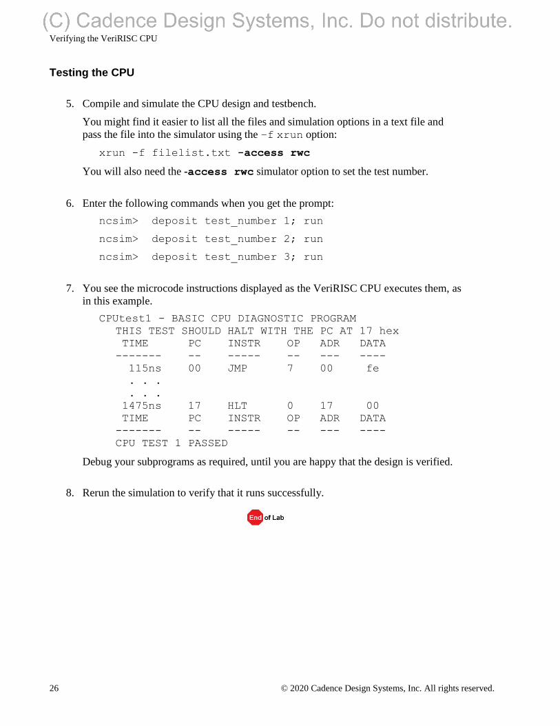
Testing the CPU
5. Compile and simulate the CPU design and testbench.
You might find it easier to list all the files and simulation options in a text file and
pass the file into the simulator using the –f xrun option:
xrun -f filelist.txt -access rwc
You will also need the -access rwc simulator option to set the test number.
6. Enter the following commands when you get the prompt:
ncsim> deposit test_number 1; run
ncsim> deposit test_number 2; run
ncsim> deposit test_number 3; run
7. You see the microcode instructions displayed as the VeriRISC CPU executes them, as
in this example.
CPUtest1 - BASIC CPU DIAGNOSTIC PROGRAM
THIS TEST SHOULD HALT WITH THE PC AT 17 hex
TIME PC INSTR OP ADR DATA
------- -- ----- -- --- ----
115ns 00 JMP 7 00 fe
. . .
. . .
1475ns 17 HLT 0 17 00
TIME PC INSTR OP ADR DATA
------- -- ----- -- --- ----
CPU TEST 1 PASSED
Debug your subprograms as required, until you are happy that the design is verified.
8. Rerun the simulation to verify that it runs successfully.
Using Scope-Based Randomization
© 2020 Cadence Design Systems, Inc. All rights reserved. 27
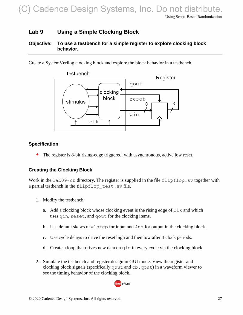
Lab 9 Using a Simple Clocking Block
Objective: To use a testbench for a simple register to explore clocking block behavior.
Create a SystemVerilog clocking block and explore the block behavior in a testbench.
Specification
The register is 8-bit rising-edge triggered, with asynchronous, active low reset.
Creating the Clocking Block
Work in the lab09-cb directory. The register is supplied in the file flipflop.sv together with
a partial testbench in the flipflop_test.sv file.
1. Modify the testbench:
a. Add a clocking block whose clocking event is the rising edge of clk and which
uses qin, reset, and qout for the clocking items.
b. Use default skews of #1step for input and 4ns for output in the clocking block.
c. Use cycle delays to drive the reset high and then low after 3 clock periods.
d. Create a loop that drives new data on qin in every cycle via the clocking block.
2. Simulate the testbench and register design in GUI mode. View the register and
clocking block signals (specifically qout and cb.qout) in a waveform viewer to
see the timing behavior of the clocking block.
Using a Simple Clocking Block
28 © 2020 Cadence Design Systems, Inc. All rights reserved.
Lab 10 Using Scope-Based Randomization
Objective: To use SystemVerilog scope-based randomization with constraints.
Modify your Memory testbench to use constrained scope-based randomization for data and address
values.
Modifying the Memory Testbench
Work in the lab10-memrnd directory.
1. Copy your Memory design, testbench, interface and top-level module from lab07-
intf into lab10-memrnd. If you did not complete Lab 8, copy the files from the
files subdirectory.
2. Add a new “Random Data” test to your testbench to write and check random data for
every address. Simulate the design to confirm the randomization.
3. Add a constraint to limit data to be a printable ASCII character (8'h20 - 8'h7F).
Modify your read and write memory debug messages to print the character generated
(use the %c format specifier). Check your constraint in simulation.
4. Add a constraint to limit data to be A-Z or a-z (8'h41-8'h5a, 8'h61-8'h7a).
Check your constraint in simulation.
5. Apply weights to the constraints so that 80% of the time randomization chooses an
uppercase letter and 20% of the time it chooses a lowercase letter. Check your
constraint in simulation.
Using Classes
© 2020 Cadence Design Systems, Inc. All rights reserved. 29
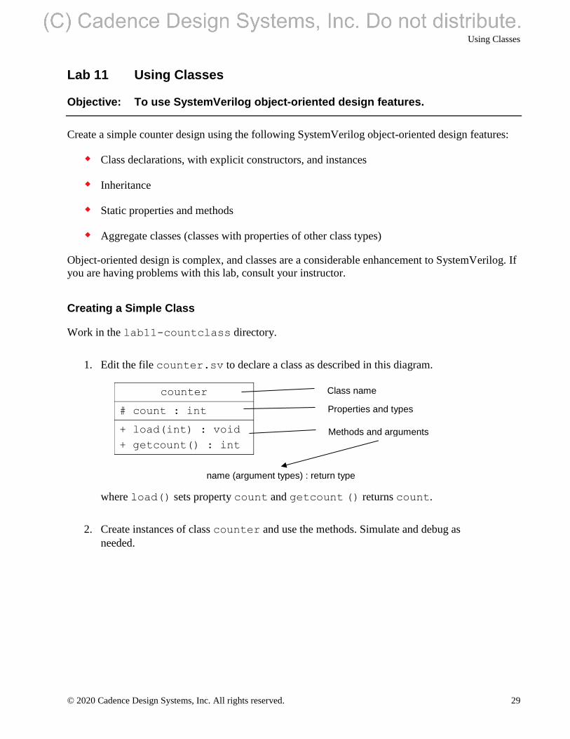
Lab 11 Using Classes
Objective: To use SystemVerilog object-oriented design features.
Create a simple counter design using the following SystemVerilog object-oriented design features:
Class declarations, with explicit constructors, and instances
Inheritance
Static properties and methods
Aggregate classes (classes with properties of other class types)
Object-oriented design is complex, and classes are a considerable enhancement to SystemVerilog. If
you are having problems with this lab, consult your instructor.
Creating a Simple Class
Work in the lab11-countclass directory.
1. Edit the file counter.sv to declare a class as described in this diagram.
where load() sets property count and getcount () returns count.
2. Create instances of class counter and use the methods. Simulate and debug as
needed.
counter
# count : int
+ load(int) : void
+ getcount() : int
Class name
Properties and types
Methods and arguments
name (argument types) : return type
Using Classes
30 © 2020 Cadence Design Systems, Inc. All rights reserved.
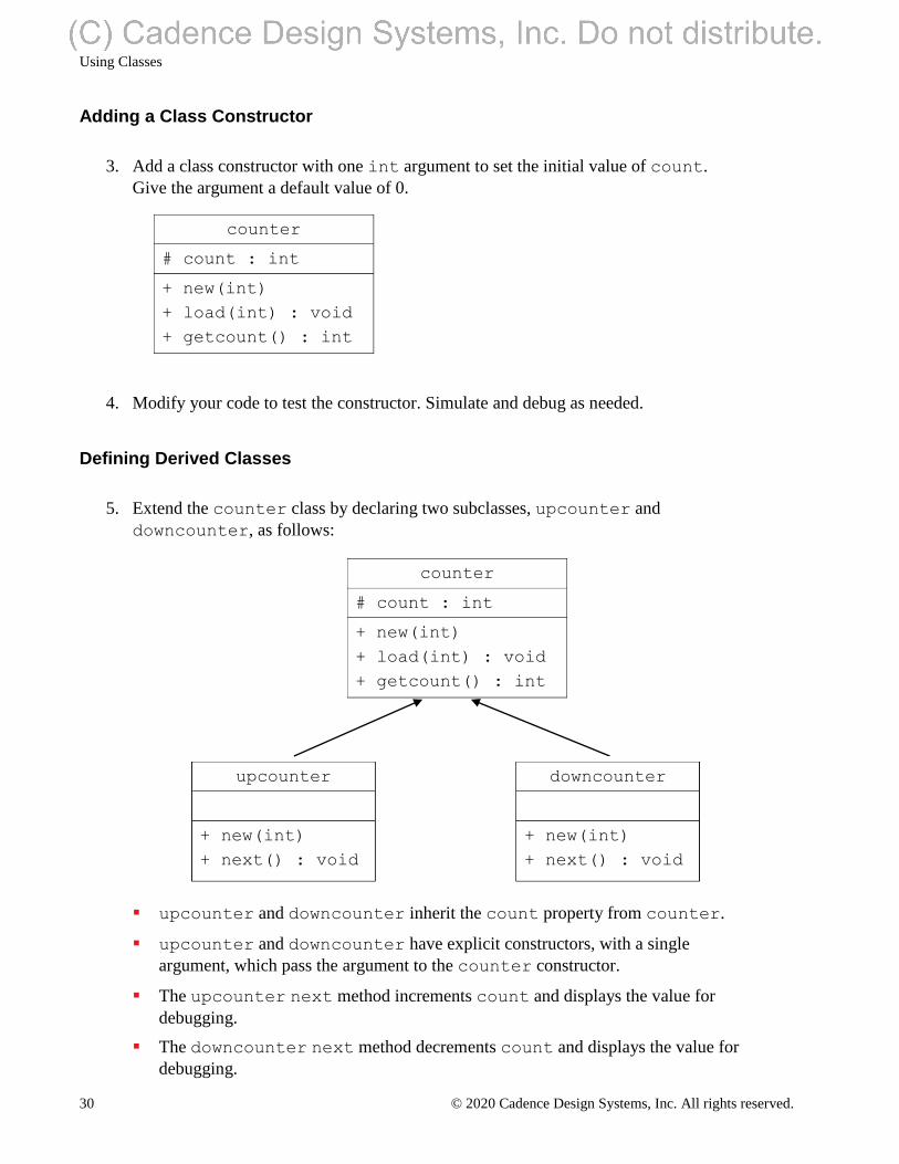
Adding a Class Constructor
3. Add a class constructor with one int argument to set the initial value of count.
Give the argument a default value of 0.
4. Modify your code to test the constructor. Simulate and debug as needed.
Defining Derived Classes
5. Extend the counter class by declaring two subclasses, upcounter and
downcounter, as follows:
▪ upcounter and downcounter inherit the count property from counter.
▪ upcounter and downcounter have explicit constructors, with a single
argument, which pass the argument to the counter constructor.
▪ The upcounter next method increments count and displays the value for
debugging.
▪ The downcounter next method decrements count and displays the value for
debugging.
counter
# count : int
+ new(int)
+ load(int) : void
+ getcount() : int
counter
# count : int
+ new(int)
+ load(int) : void
+ getcount() : int
upcounter
+ new(int)
+ next() : void
downcounter
+ new(int)
+ next() : void
Using Classes
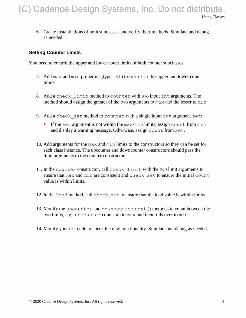
© 2020 Cadence Design Systems, Inc. All rights reserved. 31
6. Create instantiations of both subclasses and verify their methods. Simulate and debug
as needed.
Setting Counter Limits
You need to control the upper and lower count limits of both counter subclasses.
7. Add max and min properties (type int) to counter for upper and lower count
limits.
8. Add a check_limit method to counter with two input int arguments. The
method should assign the greater of the two arguments to max and the lesser to min.
9. Add a check_set method to counter with a single input int argument set:
▪ If the set argument is not within the max-min limits, assign count from min
and display a warning message. Otherwise, assign count from set.
10. Add arguments for the max and min limits to the constructors so they can be set for
each class instance. The upcounter and downcounter constructors should pass the
limit arguments to the counter constructor.
11. In the counter constructor, call check_limit with the two limit arguments to
ensure that max and min are consistent and check_set to ensure the initial count
value is within limits.
12. In the load method, call check_set to ensure that the load value is within limits.
13. Modify the upcounter and downcounter next()methods to count between the
two limits, e.g., upcounter counts up to max and then rolls over to min.
14. Modify your test code to check the new functionality. Simulate and debug as needed.
Using Classes
32 © 2020 Cadence Design Systems, Inc. All rights reserved.
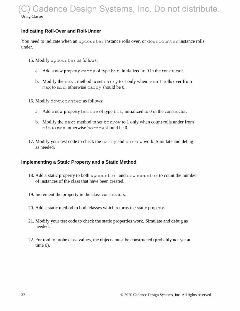
Indicating Roll-Over and Roll-Under
You need to indicate when an upcounter instance rolls over, or downcounter instance rolls
under.
15. Modify upcounter as follows:
a. Add a new property carry of type bit, initialized to 0 in the constructor.
b. Modify the next method to set carry to 1 only when count rolls over from
max to min, otherwise carry should be 0.
16. Modify downcounter as follows:
a. Add a new property borrow of type bit, initialized to 0 in the constructor.
b. Modify the next method to set borrow to 1 only when count rolls under from
min to max, otherwise borrow should be 0.
17. Modify your test code to check the carry and borrow work. Simulate and debug
as needed.
Implementing a Static Property and a Static Method
18. Add a static property to both upcounter and downcounter to count the number
of instances of the class that have been created.
19. Increment the property in the class constructors.
20. Add a static method to both classes which returns the static property.
21. Modify your test code to check the static properties work. Simulate and debug as
needed.
22. For tool to probe class values, the objects must be constructed (probably not yet at
time 0).
Using Classes
© 2020 Cadence Design Systems, Inc. All rights reserved. 33
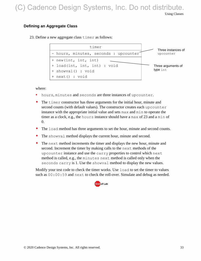
Defining an Aggregate Class
23. Define a new aggregate class timer as follows:
where:
▪ hours, minutes and seconds are three instances of upcounter.
The timer constructor has three arguments for the initial hour, minute and
second counts (with default values). The constructor creates each upcounter
instance with the appropriate initial value and sets max and min to operate the
timer as a clock, e.g., the hours instance should have a max of 23 and a min of
0.
The load method has three arguments to set the hour, minute and second counts.
The showval method displays the current hour, minute and second.
The next method increments the timer and displays the new hour, minute and
second. Increment the timer by making calls to the next methods of the
upcounter instance and use the carry properties to control which next
method is called, e.g., the minutes next method is called only when the
seconds carry is 1. Use the showval method to display the new values.
Modify your test code to check the timer works. Use load to set the timer to values
such as 00:00:59 and next to check the roll-over. Simulate and debug as needed.
timer
- hours, minutes, seconds : upcounter
+ new(int, int, int)
+ load(int, int, int) : void
+ showval() : void
+ next() : void
Three instances of upcounter
Three arguments of type int

Using Class-Based Randomization
34 © 2020 Cadence Design Systems, Inc. All rights reserved.
Lab 12 Using Class Polymorphism and Virtual Methods
Objective: To use SystemVerilog Polymorphism, Virtual Classes and Virtual Methods.
Work in the lab12-countclass directory with the counter class and its subclasses as
follows:
1. Modify the counter class to declare it as virtual.
2. Add a next method to the counter class to match the next methods in
upcounter and downcounter, so that counter next is overridden by the
next methods of the subclasses. Inside the counter next method, simply display
a message reporting that you are in the counter class.
3. Comment out your existing verification code and add new code as follows:
a. Declare a counter class handle, but do not construct an instance. As the counter
class is now virtual, trying to create an instance will generate compiler errors.
b. Create an instance of upcounter and assign this to the counter handle.
c. Call next from the counter handle.
4. Simulate and debug as needed. The next call from the counter handle should call
the counter next implementation, even though the handle contains a subclass
instance.
5. Modify your verification code as follows:
a. Declare another upcounter handle and use $cast to copy the upcounter
instance from the counter handle to this new upcounter handle.
b. Add a next call from the new upcounter handle.
6. Simulate and debug as needed. The next call from the new upcounter handle
should call the upcounter next implementation.
7. Modify your code to declare the next method of the counter class as virtual.
8. Simulate and debug as needed. Since next is now virtual you should see that calling
next from both the counter handle (containing an upcounter instance) and
from an upcounter handle are directed to the upcounter next implementation.
Using Class Polymorphism and Virtual Methods
© 2020 Cadence Design Systems, Inc. All rights reserved. 35
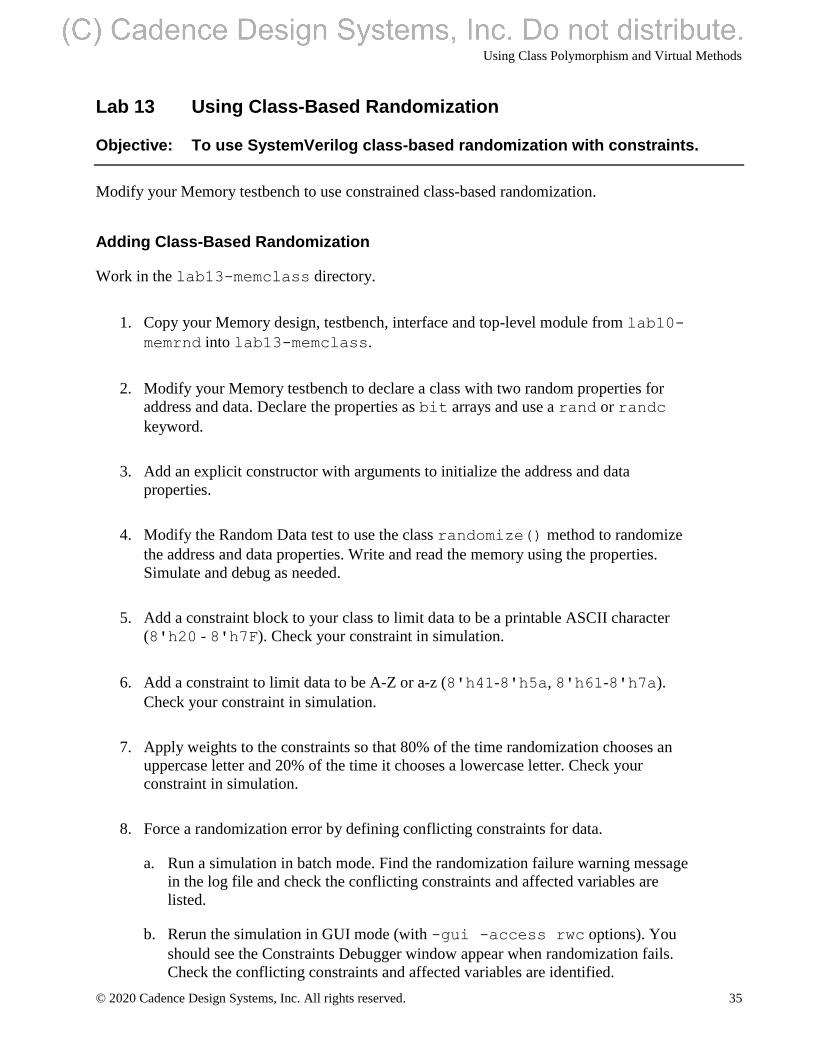
Lab 13 Using Class-Based Randomization
Objective: To use SystemVerilog class-based randomization with constraints.
Modify your Memory testbench to use constrained class-based randomization.
Adding Class-Based Randomization
Work in the lab13-memclass directory.
1. Copy your Memory design, testbench, interface and top-level module from lab10-
memrnd into lab13-memclass.
2. Modify your Memory testbench to declare a class with two random properties for
address and data. Declare the properties as bit arrays and use a rand or randc
keyword.
3. Add an explicit constructor with arguments to initialize the address and data
properties.
4. Modify the Random Data test to use the class randomize() method to randomize
the address and data properties. Write and read the memory using the properties.
Simulate and debug as needed.
5. Add a constraint block to your class to limit data to be a printable ASCII character
(8'h20 - 8'h7F). Check your constraint in simulation.
6. Add a constraint to limit data to be A-Z or a-z (8'h41-8'h5a, 8'h61-8'h7a).
Check your constraint in simulation.
7. Apply weights to the constraints so that 80% of the time randomization chooses an
uppercase letter and 20% of the time it chooses a lowercase letter. Check your
constraint in simulation.
8. Force a randomization error by defining conflicting constraints for data.
a. Run a simulation in batch mode. Find the randomization failure warning message
in the log file and check the conflicting constraints and affected variables are
listed.
b. Rerun the simulation in GUI mode (with -gui -access rwc options). You
should see the Constraints Debugger window appear when randomization fails.
Check the conflicting constraints and affected variables are identified.
Using Class-Based Randomization
36 © 2020 Cadence Design Systems, Inc. All rights reserved.
9. (Optional) Add a property to the class to conditionally control the randomization
constraints. A control property like this is known as a policy or control knob. Declare
the property as an enum type with appropriate values. Use conditional constraints to
select one of the following constraints based on the property value:
a. A printable ASCII character
b. An uppercase character A-Z
c. A lowercase character a-z
d. Either an uppercase (80% probability) or lowercase (20% probability) character
10. Simulate and debug as needed.
Using Virtual Interfaces
© 2020 Cadence Design Systems, Inc. All rights reserved. 37
Lab 14 Using Virtual Interfaces
Objective: To use virtual interface class properties and connect these to multiple instances of memories.
Modify your Memory testbench classes to use virtual interfaces to drive stimulus.
Adding a Virtual Interface
Work in the lab14-memvif directory.
1. Copy your files from lab13-memclass to lab14-memvif.
2. Modify your Memory testbench to add a virtual interface of the correct type as a class
property.
3. Move the read_mem and write_mem tasks into the class declaration. Modify the
tasks to access class properties directly (both should only have a single debug
argument). You will need to declare an additional, non-random class property to hold
the read data value.
4. Modify your write_mem and read_mem class methods to access the interface
signals via the virtual interface.
5. Define a new class method called configure which takes an input virtual interface
argument and assigns it to your virtual interface property.
6. Modify your verification code to insert a configure call between the class
construction and randomization. Use configure to set the virtual interface property
to the interface port of the testbench module. Simulate and debug as needed.
Remember the default value of a virtual interface is null, so if you do not assign the
virtual interface before use, you will “null pointer dereference” errors in simulation.
7. Remove the “Clearing the memory” and “Data = Address” tests. Modify your
Random Data test to call the simulation tasks from a class instance. Simulate and
debug as needed.
Using Virtual Interfaces
38 © 2020 Cadence Design Systems, Inc. All rights reserved.
Using a Virtual Interface with Multiple Memories (Optional)
8. Add another Memory interface port to your testbench. Copy the Random Data Test
and add a call to configure so the second test drives the new memory interface
port.
9. Add new Memory and interface instances to the top module and connect to the
testbench.
10. Simulate and debug as needed to check whether your testbench is driving both
memory instances.
Simple Covergroup Coverage
© 2020 Cadence Design Systems, Inc. All rights reserved. 39
Lab 15 Simple Covergroup Coverage
Objective: To collect and analyze data-oriented functional coverage.
Modify your Memory testbench to collect coverage on address and data values.
The simulation and coverage options described below are specific to Cadence Incisive and IMC. Ask
your trainer or consult documentation if you are using other tools.
Adding a Covergroup and Capturing Coverage
Work in the lab15-memcov directory.
1. Copy your Memory design, testbench, interface and top-level module from lab13-
memclass into lab15-memcov. For simplicity, you will not be using the virtual
interface testbench.
Check that you have the distribution constraint for data active with an 80% weight for
an uppercase letter and 20% weight for a lowercase letter.
2. Declare a covergroup in the Memory testbench module (not the class) using the
positive edge of the clock as the sampling event. In the covergroup:
a. Declare a coverpoint for the address using automatic bins.
b. Declare coverpoints for data_in and data_out, both with explicit scalar bins:
One scalar bin covering uppercase letters (8'h41-8'h5a)
One scalar bin covering lowercase letters (8'h61-8'h7a)
One scalar default bin for all other values
3. Instantiate the covergroup in the testbench.
4. Simulate your design with the following Cadence options to enable coverage
collection:
▪ -covdut mem_test Coverage scope (mem_test is the testbench module)
▪ -coverage U Coverage type (functional)
▪ -covoverwrite Overwrites existing coverage data
Simple Covergroup Coverage
40 © 2020 Cadence Design Systems, Inc. All rights reserved.
Debug as needed. If coverage is being captured correctly, you should see simulator
messages similar to the following:
coverage setup:
workdir : ./cov_work
dutinst : top.mtest(mem_test)
If running in GUI mode, you will see these messages only when the coverage tool is
invoked.
Analyzing Coverage
The following instructions use the Cadence IMC tool to analyze the coverage results. Ask your
trainer or consult tool documentation if you do not have access to IMC.
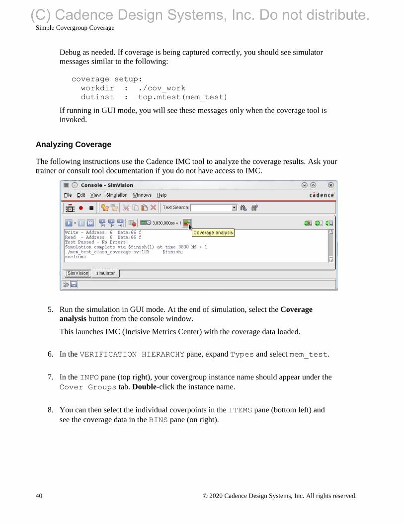
5. Run the simulation in GUI mode. At the end of simulation, select the Coverage
analysis button from the console window.
This launches IMC (Incisive Metrics Center) with the coverage data loaded.
6. In the VERIFICATION HIERARCHY pane, expand Types and select mem_test.
7. In the INFO pane (top right), your covergroup instance name should appear under the
Cover Groups tab. Double-click the instance name.
8. You can then select the individual coverpoints in the ITEMS pane (bottom left) and
see the coverage data in the BINS pane (on right).
Simple Covergroup Coverage
© 2020 Cadence Design Systems, Inc. All rights reserved. 41
9. Examine the coverage results. You should see about four times as many uppercase
data values as lowercase.
▪ Do the coverage results match your expectations?
▪ Has every address been accessed?
▪ Does the distribution of uppercase and lowercase data values match your
constraints?
▪ Do you have any other data values sampled? If so why?
There are some problems with our existing coverage model:
▪ We are sampling coverage on every rising edge of the clock, and each read or
write may take several clock cycles, therefore we have multiple samples for each
operation.
▪ We are sampling coverage for the “Clearing the Memory” and “Data Equals
Address” tests, as well as the “Random Data” test.
10. To refine your coverage model, modify your testbench as follows:
a. Use the start and stop covergroup methods to restrict coverage collection to
the Random Data test only. Simulate and recheck your coverage.
b. Remove the sampling event from the covergroup and use the sample
covergroup method to manually trigger coverage collection. Simulate and recheck
your coverage.
c. The longer you run the test, the better the data distribution should be. Try
applying more simulation vectors and see whether this affects the coverage
results.
d. Move the coverage declaration into the class. Simulate and recheck your
coverage.
Analyzing Cross Coverage
42 © 2020 Cadence Design Systems, Inc. All rights reserved.
Lab 16 Analyzing Cross Coverage (Optional)
Objective: To capture and analyze cross coverage.
Modify an ALU testbench to add cross coverage capture. You will be using the ALU design from
Lab 05. Key points of the specification are described below, but please refer to Lab 05 for full
details.
Read the specification first and then follow the instructions in the Creating the ALU Coverage
Model section.
Specification
The ALU has 2 8-bit inputs, accum, and data, and an 8-bit out put out. In
addition, there is a 3-bit input opcode which defines the ALU operation as in the
table below.
out is synchronized to the negative edge of the ALU clock and takes the following
values depending on opcode.
Opcode Encoding Output
HLT 000 accum
SKZ 001 accum
ADD 010 data + accum
AND 011 data & accum
XOR 100 data ^ accum
LDA 101 data
STO 110 accum
JMP 111 accum
Analyzing Cross Coverage
© 2020 Cadence Design Systems, Inc. All rights reserved. 43
Creating the ALU Coverage Model
Work in the lab16-alucov directory.
1. If you have completed Lab 05, copy your ALU design (alu.sv), testbench
(alu_test.sv) and package (typedefs.sv) from lab05-alu to lab16-
alucov. Otherwise, copy the files from the files subdirectory.
2. Modify the alu_test.sv module to create a covergroup. Capture the following
coverage using the stimulus supplied:
a. Cover opcode, accum and data inputs with implicit bins. Simulate with the
correct options and check every value of opcode is covered.
b. Replace the implicit bins of accum and data with 2 explicit bins for high (>
127) and low (<128) values. Simulate and check the distribution of high/low
values on each input.
c. Create cross coverage for opcode and high/low bins of accum and data.
Simulate and check the cross-coverage results.
There will be many cross-coverage bins which are superfluous. For example, the
data value is irrelevant for opcodes such as HLT and SKZ, and the accum value is
not used in an LDA operation.
d. Try to reduce the number of cross coverage bins by excluding the irrelevant
combinations as defined by the opcode table above. Try to find the most
efficient means of controlling the cross coverage bins. Simulate and check the
distribution of data and accum high/low values for each relevant opcode.
e. Modify your stimulus to cover some or all of your coverage holes.
Using Dynamic Arrays and Queues
44 © 2020 Cadence Design Systems, Inc. All rights reserved.
Lab 17 Using Dynamic Arrays and Queues
Objective: To use dynamic arrays, associative arrays and queues.
Modify your Memory testbench to implement scoreboards using dynamic arrays, associative arrays
and queues.
Work in the lab17-memarr directory.
1. Copy your files from lab15-memcov to lab17-memarr.
2. Make sure your address class property is defined using rand and not randc.
Adding a Dynamic Array Scoreboard
3. Declare a dynamic array of logic vectors of the appropriate width.
4. Initialize the dynamic array to an appropriate size and display the array size.
5. Write 32 random address/data values using a for loop. As you are writing to the
memory, store the data in the dynamic array in the index defined by its address.
6. Use a separate for loop to read back all the addresses that were written (contain non-x
data) and check the read data against the corresponding dynamic array location.
As the addresses are random, not all the memory locations will have been written, but
using logic vectors lets you use the initial unknown state to detect an unwritten
address.
7. Simulate and debug as required. Force data errors in the memory to ensure that
incorrect values are detected.
Adding an Associative Array Scoreboard
Using a contiguous dynamic array is potentially inefficient, as not all address locations will be
created by randomization. Use of an associative array may be more efficient because:
Only the address locations written to are created in the array.
We can find out how many locations need to be checked using the num method.
Using first and next methods, we can check only the locations written.
Using Dynamic Arrays and Queues
© 2020 Cadence Design Systems, Inc. All rights reserved. 45
Locations can be deleted once they have been read.
8. Modify the testbench to use an associative array rather than a dynamic array.
Make sure you use the efficiency improvements above. For example:
▪ Report the number of locations to be checked before the read memory loop.
▪ Use a do...while loop and first/next methods to read only the
addresses that have been written.
▪ Delete the addresses once they have been read and checked.
9. Simulate and debug as required. Force data errors in the memory to ensure that
incorrect values are detected.
Adding a Queue Scoreboard
A queue’s capabilities are not a good match for your scoreboard requirements. However, with
some simple changes to the stimulus, we can try various options for a queue-based scoreboard.
10. Make sure that the Random Data stimulus writes to every memory address exactly
once, for instance by defining the address randomization as randomcyclic (using
randc) or by using a for loop to generate the address and just randomizing the
data.
11. Modify the testbench to use a queue rather than an associative array. There are
various options you could try for storing the address-data pair in the queue:
▪ Declare a queue of 13-bit vectors. Concatenate the address and data prior to a
queue push and extract the address and data from the pop result.
▪ If your simulator supports queues of structures, declare a structure with an address
and data field. Declare a queue of this structure and push the address and data
during the write operation and pop the address and data for comparison during
read.
12. Simulate and debug as required. Force data errors in the memory to ensure that
incorrect values are detected.
Simulating Simple Implication Assertions
46 © 2020 Cadence Design Systems, Inc. All rights reserved.
Lab 18 Simulating Simple Implication Assertions
Objective: To create and simulate simple implication SystemVerilog assertions.
Write SystemVerilog assertions for an existing design to match an initial specification, then explore
assertion failures and rewrite your assertions to more closely match the specification.
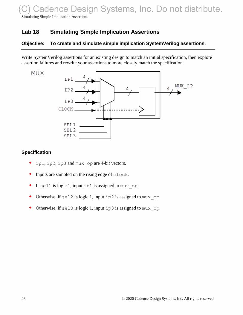
Specification
ip1, ip2, ip3 and mux_op are 4-bit vectors.
Inputs are sampled on the rising edge of clock.
If sel1 is logic 1, input ip1 is assigned to mux_op.
Otherwise, if sel2 is logic 1, input ip2 is assigned to mux_op.
Otherwise, if sel3 is logic 1, input ip3 is assigned to mux_op.
Simulating Simple Implication Assertions
© 2020 Cadence Design Systems, Inc. All rights reserved. 47
Creating the Assertions
Work in the lab18-svamux directory.
1. A model for the MUX is provided in the mux.sv file. In this file, assert three
properties, evaluated only on the active edge (rising edge) of the signal clock, to do
the following:
a. When sel1 is 1’b1, check that in the next evaluation cycle mux_op equals ip1
from the past cycle" (i.e. use $past()).
b. When sel2 is 1’b1, check that in the next evaluation cycle mux_op equals ip2
from the past cycle" (i.e. use $past()).
c. When sel3 is 1’b1, check that in the next evaluation cycle mux_op equals ip3
from the past cycle" (i.e. use $past()).
At this stage, please write the properties to meet the specification above (what the lab book asks
for), rather than how you might think the properties should be defined.
Simulating Your Assertions
2. Examine the MUX testbench file, mux_test.sv. The first part of the testbench
floats a logic 1 across each of the MUX select inputs. The second part of the
testbench increments the MUX select inputs through all possible combinations.
3. Simulate your design in GUI mode using the following xrun options:
xrun mux.sv mux_test.sv -gui -access +rwc -linedebug
4. Before running simulation, set a simulation breakpoint on the first executable line
after this comment in the testbench mux_test.sv:
//Set a breakpoint on next executable line.
5. Find and open the Assertion Browser window and check whether your assertions
appear. Use the browser to add your assertions to the waveform window.
6. Use the Design Browser to add the assertion testbench signals to the waveform
window.
7. Simulate with the 1st set of test vectors by running up to the breakpoint.
Simulating Simple Implication Assertions
48 © 2020 Cadence Design Systems, Inc. All rights reserved.
8. Verify that your asserted properties hold for all stimuli applied up to the breakpoint.
Assertion failures will be reported by the simulator and can be viewed in the
Waveform window.
There are several ways to view assertions in the waveform window, including
displaying assertions as transactions. Ask your trainer or consult tool documentation.
9. Run the simulator from the breakpoint until the end of simulation.
Note that the simulator may stop every time a property fails or a breakpoint is hit.
Keep running until the end of simulation as indicated by a message in the command
window.
10. Your second and third property assertions have failed. Why?
Hint: Look at the properties in the waveform viewer and check when the properties
fail.
Modifying the Assertions
The property specification provided above is incomplete. The properties did not consider the priority
of the selx select inputs, as specified in the Functionality section above (look at the properties in
the waveform viewer to see what the inputs are when the assertions failed).
11. Edit your assertions to account for the selx priority.
12. Rerun the simulation (remember to continue past the breakpoint).
13. Confirm that your new properties hold throughout the simulation.
Conclusions
One of the aims of this exercise is to teach you an important lesson on assertions. Assertions are
ineffective if:
The test data is incomplete, as in the first set of stimuli.
The assertions are incorrectly written, as with our initial properties.
Sequence-Based Properties
© 2020 Cadence Design Systems, Inc. All rights reserved. 49
Lab 19 Sequence-Based Properties
Objective: To create and simulate sequence-based assertions.
Create a simple and a complex sequence-based assertion and simulate them with a supplied
testbench to explore how your simulator handles and reports the various states in a multi-cycle
assertion evaluation.
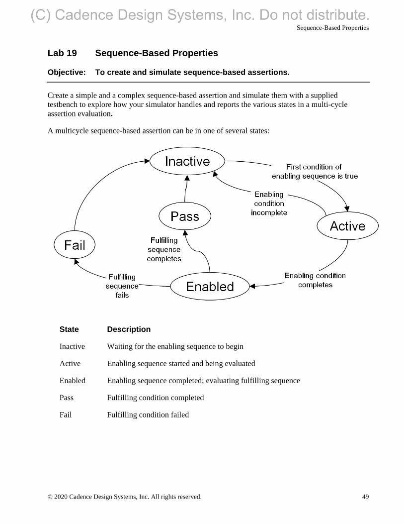
A multicycle sequence-based assertion can be in one of several states:
State Description
Inactive Waiting for the enabling sequence to begin
Active Enabling sequence started and being evaluated
Enabled Enabling sequence completed; evaluating fulfilling sequence
Pass Fulfilling condition completed
Fail Fulfilling condition failed
Sequence-Based Properties
50 © 2020 Cadence Design Systems, Inc. All rights reserved.
Creating the Simple Sequence Assertion
Work in the lab19-svaseq directory, editing the seqtest.sv file.
1. Create and assert a property SIMPLE_SEQ, clocked off the negative edge of CLK, to
the following specification:
a. The enabling sequence is A at logic 1 followed immediately by B at logic 1
followed immediately by C at logic 1 (in consecutive samples).
b. The fulfilling sequence follows in the cycle after the enabling sequence
completes, and is J at logic 1 followed by K at logic 1 in consecutive samples.
c. The property is disabled if X is at logic 1 for any cycle.
2. Examine the rest of the testbench and make sure you understand its operation.
Note that for each subtest, the testbench passes a character string to a subprogram
do_test. The ; character is the cycle delimiter. Other characters correspond to
signals driven high by the subprogram during that clock cycle.
Leave the commented out section – this is for testing the complex sequence.
3. Simulate your design in GUI mode using the following xrun options:
xrun seqtest.sv -gui –access +rwc –linedebug
4. Set a breakpoint at the line which contains breakpoint=breakpoint+1 in the
task do_test. You can use this breakpoint to step through the subtests. The
simulator will otherwise stop at only the failing tests.
5. Run the simulation. If you have successfully created the simple sequence assertion,
you should see three assertion failures. Two of the failures occur within the same
subtest.
6. Rerun the simulation up to the first failing subtest.
Question 1 – Which subtest failed and why did it fail?
.......................................................................................................................
Hint: Use the waveform viewer to examine the signal in the sequence and the states
of the assertion. Compare this failing test to previous passing tests.
7. Run the simulation up to the second failing subtest.
Question 2 – Which subtest failed and why did it fail?
.......................................................................................................................
Sequence-Based Properties
© 2020 Cadence Design Systems, Inc. All rights reserved. 51
Creating the Complex Sequence Assertion
8. Add a complex sequence assertion COMPLEX_SEQ, clocked off the negative edge of
CLK, to the following specification:
a. The enabling sequence is C at logic 1 followed immediately by between one and
three samples in which B is at logic 1 followed immediately by A at logic 1.
b. The fulfilling sequence follows in the cycle after the enabling sequence
completes, and is J at logic 1 for four samples, the last of which is followed
immediately in the next sample by K at logic 1.
c. The assertion is disabled if X is at logic 1 for any cycle.
9. Comment out the stimulus for the simple sequence assertion and un-comment the
stimulus for the complex assertion.
Compile seqtest.sv, fix any compilation errors and load into the simulator. You
can set a breakpoint on the signal breakpoint to step through the subtests.
10. Run the stimulation. If you have successfully created the complex sequence assertion,
you should see one failure when you simulate the design:
11. Run the simulation up to the failing test.
Question 3 – Which subtest failed and why did it fail?
.......................................................................................................................
12. Add stimuli to explore and demonstrate answers to the following questions:
Question 4 – If a K occurs in the same cycle as the fourth J, e.g.:
C;B;B;A;J;J;J;JK;;
When and why does the assertion fail?
.......................................................................................................................
Question 5 – If multiple As occur in the same cycles as the second and third Bs, as
seen in this example:
C;B;BA;BA;A;J;J;J;J;K;
How many assertions are enabled? How many fail? When and why do they fail?
.......................................................................................................................
Question 6 – How can you modify the stimulus of the Question 5 to ensure all
assertions pass?
.......................................................................................................................
Sequence-Based Properties
52 © 2020 Cadence Design Systems, Inc. All rights reserved.
Answers to Questions
Question 1 – Which test failed and why did it fail?
The 3rd subtest of the simple assertion fails to complete the fulfilling sequence – J is
not immediately followed by K.
Question 2 – Which test failed and why did it fail?
The 5th subtest of the simple assertion fails to complete the fulfilling sequence for
two overlapping traces of the sequence. Both traces fail because K does not
immediately follow J. These two failures occur in consecutive cycles.
Question 3 – Which test failed and why did it fail?
The 6th subtest of the complex assertion fails to complete the fulfilling sequence – K
does not immediately follow the fourth occurrence of J.
Question 4 – If a K occurs in the same cycle as the fourth J, when and why does the assertion fail?
The assertion fails on the cycle following the 4th occurrence of J. K is not checked on
the fourth occurrence of J but is checked in the cycle immediately following. As K is
not found, the assertion fails.
Question 5 – If multiple As occur in the same cycles as the second and third Bs, that is, from the
stimulus:
C;B;BA;BA;A;J;J;J;J;K;
How many assertions are enabled? How many fail? When and why do they fail?
Three attempts start on cycle 1 and are enabled, at cycles 3, 4 and 5 of the above
stimulus. The copy enabled on cycle 4 and cycle 3 fails because, the first condition of
the fulfilling sequence, does not occur. The copy enabled on cycle 5 completes
successfully.
Question 6 – How can you modify the stimulus of Question 5 to ensure all assertions pass?
The following stimulus passes all the assertions:
C;B;BA;BA;AJ;J;J;J;JK;K;
Synchronizing Processes with a Mailbox
© 2020 Cadence Design Systems, Inc. All rights reserved. 53
Lab 20 Simple DPI Use
Objective: To import simple C functions into SystemVerilog code.
Import C functions from the standard and math C libraries and execute in SystemVerilog code.
Work in the lab20-simpledpi directory:
1. The stdlibs.c file simply includes the standard and math C libraries.
2. Create a module dpi in a dpi.sv file and import the following C functions to
appropriate SystemVerilog function declarations:
a. system – Executes a command on the operating system. The C definition is:
int system (const char* command);
Where the input command is a string containing the system command. The return
int type depends on the command executed (can be ignored in the call).
b. getenv – Returns the value of an environmental variable. The C definition is:
char* getenv (const char* name);
Where the input name is a string containing the environmental variable name. The
return string type contains the variable value.
c. sin – Returns the sine of an angle. The C definition is:
double sin (double x);
Where the input x is the angle in radians. The return real type is the sine value.
3. Add code to test your imported C functions, by, for example:
a. Executing the system command echo ‘Hello World’.
b. Execute date to print the current time and day.
c. Displaying the PATH environmental variable.
d. Displaying the first eight sine values at Π/4 intervals (see math.sv for
constants).
4. We can use the Cadence simulator to compile and simulate both C and
SystemVerilog code as follows:
xrun stdlibs.c dpi.sv
Check your results and debug as required.
Synchronizing Processes with a Mailbox
54 © 2020 Cadence Design Systems, Inc. All rights reserved.
Lab 21 Synchronizing Processes with a Mailbox
Objective: To use a mailbox to synchronize the communication of transactions between processes.
This lab provides a system in which a producer mails transactions to a consumer. At random
intervals, the producer generates communication, configuration and synchronization transactions.
The lab uses a mailbox instead of a queue because a mailbox can contain different message types.
The consumer requires random amounts of time to consume each transaction. It can simultaneously
consume one transaction of each type. It records each transaction to the terminal and log file.
Examining the Mailbox Test Case
Work in the lab21-mailbox directory.
1. Examine the transaction classes defined in the ex_trans_pkg package in the
ex_trans_pkg.sv file:
The my_tr_base_c class provides a base class that other transaction types
extend. The base class has an “id” field and a virtual get_type() method.
The my_tr_config_c, my_tr_synch_c and my_tr_comms_c classes
extend the my_tr_base_c class. The only important thing that they do is re-
implement the get_type() method.
2. Examine the mailbox_if interface in the mailbox_if.sv file:
This unit declares a mailbox and duplicates the mailbox access methods. Wrapping an
interface around a mailbox allows you to access the mailbox through ports and using
hierarchical references. This file is incomplete and you will complete it in the lab.
3. Examine the mailbox_producer_m module in the
mailbox_producer_m.sv file:
This unit randomly produces transactions and calls interface methods to put the
transactions into the interface mailbox. It produces transactions at exponentially
distributed intervals to mimic a classic Poisson arrival process. The transactions are
weighted as follows: 10% my_tr_config_c, 20% my_tr_synch_c and 70%
my_tr_comms_c.
Synchronizing Processes with a Mailbox
© 2020 Cadence Design Systems, Inc. All rights reserved. 55
4. Examine the mailbox_consumer_m module in the
mailbox_consumer_m.sv file:
This unit calls interface methods to get transactions from the interface mailbox and
separately queues each transaction type for its consumption process. It uses mailbox
queues because the SystemVerilog queue has no blocking put() and get()
methods. The service time is a uniform distribution that is the same for all transaction
types. Depending upon what system you model, you might want to alternatively
consider exponential or normal distributions of service time.
5. Examine the mailbox_top_m module in the mailbox_top_m.sv file:
This unit instantiates and connects the producer, interface and consumer and
overrides their parameters.
Completing and Simulating the Mailbox Test Case
6. Complete the mailbox_if.sv file according to the commented instructions to
declare a mailbox and complete the set of mailbox access routines.
7. Simulate your work (debug as needed).
Upon simulation, you should see randomly distributed transaction “start” and “end”
times and that the consumption of the different types of transactions can overlap.
Synchronizing Processes with a Semaphore
56 © 2020 Cadence Design Systems, Inc. All rights reserved.
Lab 22 Synchronizing Processes with a Semaphore
Objective: To use a semaphore to synchronize the use by multiple processes of a resource that can support only one process at a time.
This lab models a limited resource with two users that at random intervals attempt to use the
resource for a random amount of simulation time. To verify proper sharing of the resource, it
contains a shared variable that each user, upon entry to the limited resource, sets to a random value,
and upon exit from the resource, verifies that the value has not changed.
Completing and Simulating the Semaphore Test Case
Work in the lab22-semaphore directory.
1. Edit the semaphore_m.sv file to complete the semaphore test case according to
the commented instructions to:
a. Insert statements as instructed to instantiate and initialize the semaphore.
b. Verify that the semaphore is constructed.
c. Get the semaphore key (blocking and nonblocking).
d. Put the key back.
2. Simulate the test case and debug your work as needed.
3. Examine the log file.
You see that at no time is the resource simultaneously used by both users.
Synchronizing Processes with a Semaphore
© 2020 Cadence Design Systems, Inc. All rights reserved. 57
Lab 23 Synchronizing Processes with Events (Optional)
Objective: To use blocking and nonblocking event triggers.
This lab illustrates a situation that is very common when using blocking assignments to registers and
also applies when using blocking event triggers.
A process writes a register (or triggers an event) in exactly the same evaluation phase as another
process reads the register (or waits for the event). Any simulator can choose to evaluate either
process first. The second process might or might not be waiting for the event when it occurs.
Resolving an Undefined Process Execution Order (Race) Condition
Work in the lab23-event directory.
1. Simulate the existing event_m_1.sv source.
Examine the order in which processes trigger events, wait for events and receive
events. It is very likely that one process will wait for an event after it has occurred
and thus will not report that it saw the event.
2. Modify the event_m_1.sv source to use the nonblocking event trigger and again
simulate it.
Examine the order in which processes trigger events, wait for events and receive
events. As the events do not actually occur until the NBA region, both processes are
waiting for their events before the events actual occur, so both processes report seeing
their event.
3. Modify the event_m_1.sv source to again use the blocking event trigger, but this
time replace the @ event guard with an asynchronous wait(...) for the
triggered state of the event. Simulate the test again.
Examine the order in which processes trigger events, wait for events and receive
events. Events can trigger before a process waits for it, but if the processes instead
wait for the triggered property, they will both report seeing the event because the
triggered property of the event persists until the end of the timeslice.