Embed Size (px)
Citation preview

12334
5578
99
111213
141616
171819
20
Table of Contents
Table of ContentsBi2Se3 topological insulator
Build the Bi2Se3 crystalLatticeBasis
Bi2Se3 bulk band structureGGA calculationSOGGA calculationResults
Bi2Se3 surface: Spin-orbit band structureConstructing the surfaceDFT-SOGGA calculationsConvenient Python scriptResults
DOS analysis: Dirac cone finger printPenetration depth of surface states
Calculations
Fermi surface and spin directionsTopological Invariants
Python script for the calculating the topological invariants
References
Downloads & LinksDownloads & Links
PDF version Tutorial Synopsis Bi2Se3_ bulk_ configurat ion.py Bi2Se3_ bulk.py Bi2Se3_ slab.py dos.py bloch_ states.py spinVector.py fermi_ surface.py TopologicalInvariant3D.py Basic QuantumATK Tutorial ATK Reference Manual Basic QuantumATK Performance Guide
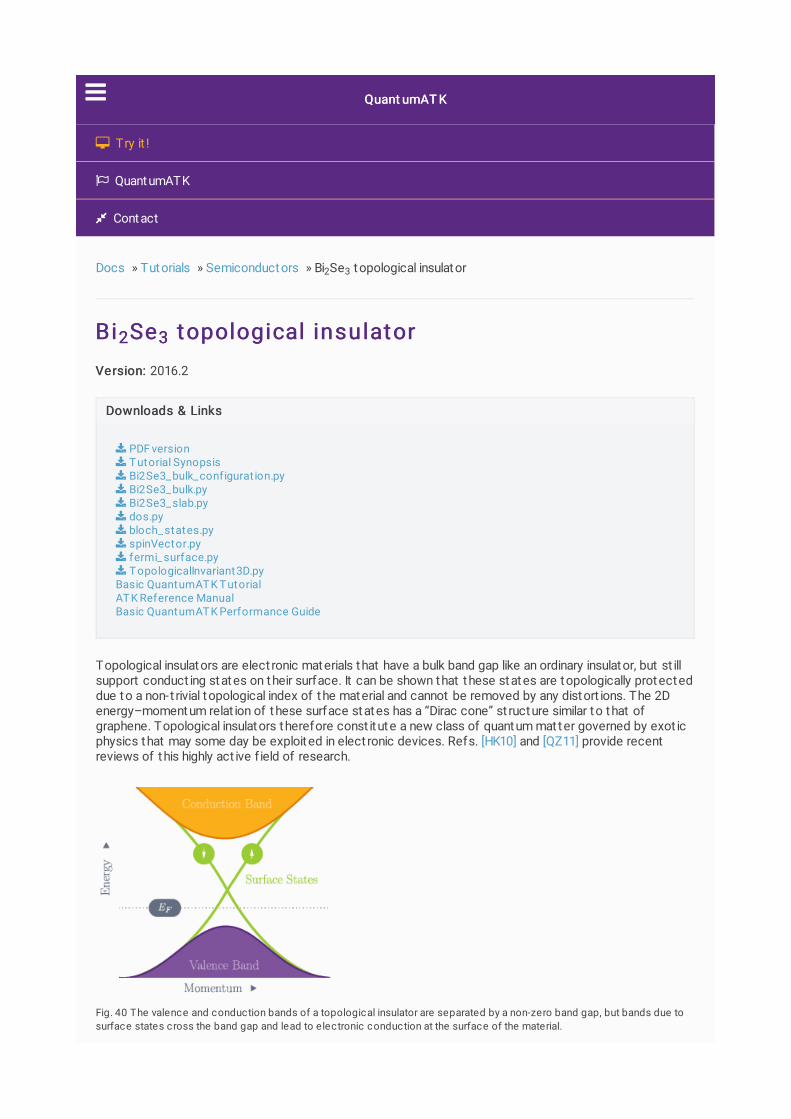
Docs » Tutorials » Semiconductors » Bi Se topological insulator
BiBi SeSe topological insulator topological insulatorVersion:Version: 2016.2
Topological insulators are elect ronic materials that have a bulk band gap like an ordinary insulator, but st illsupport conduct ing states on their surface. It can be shown that these states are topologically protecteddue to a non-t rivial topological index of the material and cannot be removed by any distort ions. The 2Denergy–momentum relat ion of these surface states has a “Dirac cone” st ructure similar to that ofgraphene. Topological insulators therefore const itute a new class of quantum matter governed by exot icphysics that may some day be exploited in elect ronic devices. Refs. [HK10] and [QZ11] provide recentreviews of this highly act ive f ield of research.
Fig. 40 The valence and conduction bands of a topological insulator are separated by a non-zero band gap, but bands due tosurface states cross the band gap and lead to electronic conduction at the surface of the material.
Quant umAT KQuant umAT K
Try it !
QuantumATK
Contact
2 3
22 33

In this tutorial you will learn how to use ATK-DFT to study the Bi Se compound, which is a 3D st rongtopological insulator. Nonequilibrium Green’s funct ion DFT calculat ions were recent ly reported for a Bi Sethin f ilm connected to leads in a two-terminal device setup [CMS+15]. However, this tutorial focuses onbulk calculat ions and propert ies of the surface states. In part icular, you will:
Use the QuantumATK Crystal Builder to construct the Bi Se crystal st ructure.Invest igate the bulk Bi Se band st ructure with and without the SOC.Construct a Bi Se slab configurat ion and compute the SOC band st ructure, which exhibits the surfacestates ment ioned above.Compute the density of states (DOS) around the Fermi energy, which nicely illust rates the Dirac coneinside the bulk band gap.Invest igate the surface state penetrat ion depth into the material.Plot the spin-resolved Fermi surface of surface states, and invest igate how the in-plane spinorientat ion varies on the Fermi surface.Calculate the topological invariants for Bi Se .
Not eNot e
It is essent ial to include the spin-orbit coupling (SOC) to correct ly describe the elect ronic st ructure ofa topological insulator.
Build t he BiBu ild t he Bi SeSe cryst al cryst al
Open the QuantumATK Builder and click Add ‣ From Plugin ‣ Crystal Builder. As described in [ZYZ+10],the Bi Se crystal is rhombohedral and belongs to space group
. It has lat t ice constants a=4.138 Å and c=28.64 Å, and internal coordinates=0.399 for Bi sites and=0.206 for Se sites. The basic Bi Se unit cell, called a quintuple layer (QL), contains 5 atoms: One Se
atom at coordinate (0, 0, 0), Bi atoms at internal coordinates, and Se atoms at
.
Lat t i c eLat t i c e
In the Crystal Builder, choose the Trigonal space group number 166 with Hexagonal set t ing, and enter thelat t ice parameters:
2 32 3
2 3
2 3
2 3
2 3
22 33
2 3
R¯̄¯3 mμν 2 3
(±μ, ±μ, ±μ)(±ν, ±ν, ±ν)
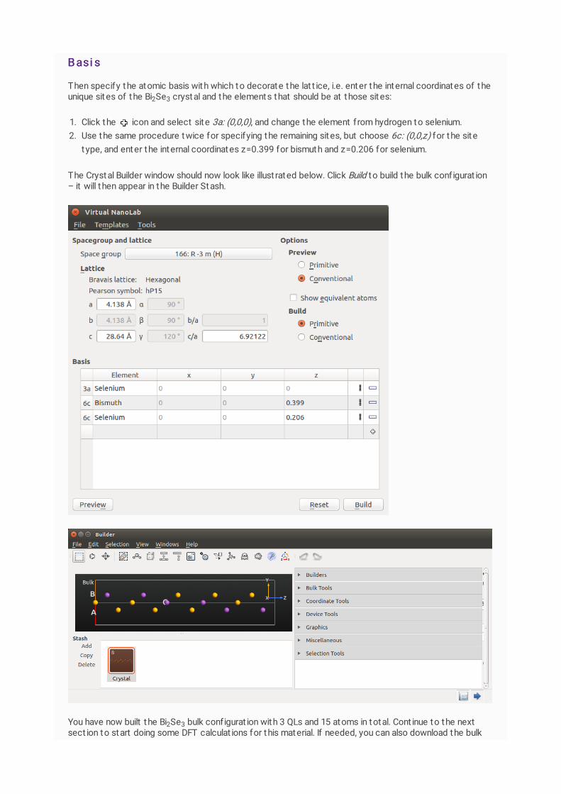
B asi sB asi s
Then specify the atomic basis with which to decorate the lat t ice, i.e. enter the internal coordinates of theunique sites of the Bi Se crystal and the elements that should be at those sites:
1. Click the icon and select site 3a: (0,0,0), and change the element from hydrogen to selenium.2. Use the same procedure twice for specifying the remaining sites, but choose 6c: (0,0,z) for the site
type, and enter the internal coordinates z=0.399 for bismuth and z=0.206 for selenium.
The Crystal Builder window should now look like illust rated below. Click Build to build the bulk configurat ion– it will then appear in the Builder Stash.
You have now built the Bi Se bulk configurat ion with 3 QLs and 15 atoms in total. Cont inue to the nextsect ion to start doing some DFT calculat ions for this material. If needed, you can also download the bulk
2 3
2 3

configurat ion here: Bi2Se3_bulk_configurat ion.py
BiBi SeSe bu lk band st ruct ure bu lk band st ruct ure
Send the bulk configurat ion to the Script Generator, and set up a Python script that uses ATK-DFT tocalculate the band st ructure with and without the spin-orbit coupling. The script should f irst calculate theself-consistent GGA state and perform band st ructure analysis, and then use that state as an init ial guessfor the self-consistent SOGGA state, again followed by band st ructure analysis.
The Script Generator now contains the bulk configurat ion. Add the New Calculator, Analysis ‣Bandstructure, and Init ial State blocks, as illust rated below. Also change the default output f ile toBi2Se3_bulk.nc .
GGA c al c ul at i o nGGA c al c ul at i o n
Open the f irst New Calculator block to edit it :
Make sure to choose the ATK-DFT calculator.In the Basis set/exchange correlat ion set t ings, choose GGA and change the pseudopotent ials to theOMX family with Medium basis sets for both Se and Bi.In the Basic set t ings tab, increase the density mesh cut -off to 150 Hart ree, and set up a 9x9x3 k-pointgrid. Click OK to save the set t ings.
22 33

Then open the f irst Bandstructure block and edit it :
Increase points per segment to 51 to get a nicely resolved band st ructure.Change the Brillouin zone route to K, G, M, G, L.Change the IO f ile to bulk_bs_gga.nc .

SOGGA c al c ul at i o nSOGGA c al c ul at i o n
Open the second New Calculator block, and edit it such that the set t ings are ident ical to those in thefirst calculator, but set the Spin parameter to Noncollinear Spin-Orbit in order to do a SOGGA calculat ion.Remember to also set the pseudopotent ials, density cut -off , and k-points.
Next , open the second Init ial State block, and select User spin for Init ial state type, t ick the Use oldcalculat ion opt ion, and enter the f ile name Bi2Se3_bulk.nc from which the GGA state should be read.

Finally, set up the second Bandstructure block ident ically to the f irst one, but use bulk_bs_sogga.nc forthe IO f ile.
R e sul t sR e sul t s
The Python script is now ready. Save it as Bi2Se3_bulk.py . If needed, you can also download it here: Bi2Se3_bulk.py
Execute it using the Job Manager or in a Terminal. The job will take a while, but the wall t ime can bebrought down to around 40 minutes if executed in parallel with 2 MPI processes on 2 CPUs. Note that thisrequires in total about 15 GB of available memory!
T ipT ip
The tutorial Basic QuantumATK Performance Guide offers t ips on QuantumATK performance, includinghow to deal with memory issues.
Once the calculat ion has f inished, the QuantumATK LabFloorLabFloor contains three sets of data: Bi2Se3_bulk,bulk_bs_gga, and bulk_bs_sogga. The last two contain the GGA and SOGGA band st ructures. Highlightboth band st ructure objects, and use the Compare Dat aCompare Dat a plugin to plot both of them.

The plot is shown below. Including spin-orbit coupling in the calculat ions (SOGGA) has a signif icant impacton the band st ructure, and widens the direct band gap at the
-point However, we do not see any bands crossing the Fermi level (the smallest SOGGA band gap is 0.3eV), so the Bi Se bulk material is an insulator.
Fig. 41 Comparison of the GGA (blue) and SOGGA (green) band structures of bulk Bi Se .
Bi2Se3 sur face: Spin - orb it band st ruct ureBi2Se3 sur face: Spin - orb it band st ruct ure
You will now create a Bi Se slab configurat ion, and compute the SOGGA band st ructure, which will exhibitthe topologically protected surface states crossing the band gap around the
-point .
Co nst ruc t i ng t he sur f ac eCo nst ruc t i ng t he sur f ac e
Back in the BuilderBuilder, highlight the Bi Se bulk configurat ion (named Crystal), and open the Builders ‣ Surface(Cleave) plugin. Choose Miller indices (0001), and select selenium atom #12 as the top atom in the slab.Then click Next .
Γ2 3
2 3
2 3
Γ
2 3

Leave set t ings at defaults in the “Define surface lat t ice” opt ions window. In the “Finalize outputconfigurat ion” opt ions, choose a Non-periodic and normal (slab) out -of-plane cell vector, and enter 10 Å forboth top and bot tom vacuum. Then click Finish.
The slab configurat ion, named Crystal (0001), has now appeared in the Stash. As a f inal touch, highlight theitem and use the Bulk Tools ‣ Lat t ice Parameters plugin to convert the lat t ice type to Hexagonal whilekeeping the fract ional coordinates constant :

DF T - SOGGA c al c ul at i o nsDF T - SOGGA c al c ul at i o ns
You can now send the slab configurat ion to the Script Generat orScript Generat or, and set up the SOGGA band st ructurecalculat ion similarly to what you did above for the bulk, but with slight changes:
You will not need the GGA band st ructure analysis.Use Bi2Se3_slab.nc as default output f ile.Use a 9x9x1 k-point grid (the slab is not periodic along the C-direct ion).Decrease the elect ron temperature from 300 to 50 K. This will improve the DFT descript ion of elect ronoccupat ions close to the Fermi level.Use 201 points per segment for the SOGGA band st ructure analysis, and the K–G–M Brillouin zoneroute.
Alt ernat ively , you can simply skip t he above and go direct ly t o t he next sect ion t o use a pre-Alt ernat ively , you can simply skip t he above and go direct ly t o t he next sect ion t o use a pre-made Pyt hon script wit h a f ew addit ional f eat ures.made Pyt hon script wit h a f ew addit ional f eat ures.

Co nve ni e nt P yt ho n sc r i ptCo nve ni e nt P yt ho n sc r i pt
Click here: Bi2Se3_slab.py to download a Python script that was made using the procedure out linedabove, but also has a few ext ra features:
The “MemoryUsage” funct ionality is used to est imate the memory required for the GGA and SOGGAcalculat ions immediately before they are executed.The SOGGA calculator is const ructed as a copy of the GGA calculator, and is then modif iedaccordingly.A special density mixing algorithm is used for the non-collinear calculat ion.
Run the calculat ion using the Job Manager or in a Terminal. The job will take roughly 30 minutes ifexecuted in 2 parallel MPI processes on 2 CPUs.
HintHint
If you look at the log f ile during the calculat ion, you will see that the est imated peak memoryrequirements are 756 MB per MPI process for the GGA calculat ion, and 3.8 GB per MPI process for theSOGGA calculat ion. These are est imates, and in pract ice you should expect the full calculat ion to

require almost 5 GB per MPI process.
GGA:+----------------------------------------------------------+| Memory usage estimate || -------------------------------------------------------- || Base: Sparse matrices 44 Mbyte || Base: GridTool+Basis set 100 Mbyte || Base: SCF history 442 Mbyte || Base: NLEngine 70 Mbyte || Base: Grid terms 39 Mbyte || Sum of the base terms 696 Mbyte || -------------------------------------------------------- || Peak: Diagonalization 60 Mbyte || Peak: Grid terms 19 Mbyte || -------------------------------------------------------- || Estimated Peak memory requirement 756 Mbyte |+----------------------------------------------------------+
SOGGA:+----------------------------------------------------------+| Memory usage estimate || -------------------------------------------------------- || Base: Sparse matrices 272 Mbyte || Base: GridTool+Basis set 100 Mbyte || Base: SCF history 2726 Mbyte || Base: NLEngine 70 Mbyte || Base: Grid terms 157 Mbyte || Sum of the base terms 3326 Mbyte || -------------------------------------------------------- || Peak: Diagonalization 446 Mbyte || Peak: Grid terms 58 Mbyte || -------------------------------------------------------- || Estimated Peak memory requirement 3772 Mbyte |+----------------------------------------------------------+
R e sul t sR e sul t s
The QuantumATK LabFloorLabFloor should now contain the results of the calculat ion. Select the band st ructureobject , and use the Bandst ruct ure Analyz erBandst ruct ure Analyz er to plot it .
The calculated band st ructure of the Bi Se slab is shown below. Bands are now present around the Fermilevel at the
-point – these are surface states. There are four such surface states crossing the Fermi level (indicatedby red dots); bands 142 and 143 form a single degenerate band immediately below the Fermi energy, whilebands 144 and 145 form a degenerate band above E . The bulk valence bands are below those surfacestates (indicated by blue dot). It is clear that the dirac cone is located inside the bulk band gap. There is at iny gap between the valence and conduct ion surface bands of size 7 meV. This is a f inite size effect
2 3
Γ
F

from the use of a slab model, which arise from the interact ion of the surface bands on opposite sides ofthe slab. For a larger slab the gap will be reduced.
Fig. 42 SOGGA bandstructure of the Bi Se slab configuration. The bottom panel is a zoom-in on the topologically protectedDirac cone. Both surface state bands (red dots) are both doubly degenerate and are located above the bulk valence bands(blue dot).
DOS analysis: Dirac cone f inger pr in tDOS analysis: Dirac cone f inger pr in t
As stated in the int roduct ion, the elect ronic st ructure of the surface states close to the Fermi levelresembles that of a Dirac cone, where the elect ron momentum depends linearly on the energy. Since thesurface states are the only states present inside the bulk energy gap, we should expect the elect ronicdensity of states close to E to be linear. It is easy to compute and plot the DOS as a post -SCF analysis:
Open the Script Generat orScript Generat or and add the Analysis from File and Analysis ‣ DensityOfStates blocks.Change the default output f ile to dos.nc .
2 3
F

Open the f irst block, and point to the Bi2Se3_slab.nc f ile and Object id glD001, which is the self-consistent SOGGA state.
Then open the DensityOfStates analysis block, and set up a dense k-point sampling along k and k ,21x21x1. You will need to uncheck the sync opt ion. Remember: It is important in this case to sample the
-point , so we use use an odd k-grid.
Save the script as dos.py and run it . You can also download it here: dos.py.
Then locate the DOS object on the LabFloorLabFloor, and use the 2D Plot2D Plot plugin to visualize it . With a bit ofzooming you should be able to see the expected linear dependence of the DOS on energy, as illust ratedbelow. The sharp increase in DOS at E=0.47 eV are due to the lowest bulk conduct ion bands.
x y
Γ

Fig. 43 Electronic DOS for the Bi Se slab. Due to the Dirac cone, the DOS depends linearly on the energy in the vicinity of theFermi level.
Penet rat ion dept h of sur face st at esPenet rat ion dept h of sur face st at es
An essent ial feature of the topologically protected surface states close to the Dirac point is that they arehighly localized to the surface region. The penetrat ion depth into the bulk material may be as small as 2–3nm [ZYZ+10]. Moreover, the degenerate surface states observed in a band st ructure calculat ion are ineach specif ic k-point composed of states with opposite spin and localized on opposite sides of the slab.
You will now invest igate this by performing a BlochSt at e analysisBlochSt at e analysis in a specif ic k-point on the Dirac conefor bands 144 and 145. You will then project both Bloch states onto the C-axis of the Bi Se slab unit cell,and plot the magnitude and direct ion of the non-collinear spin vectors as a funct ion of the C-coordinate.
Cal c ul at i o nsCal c ul at i o ns
You will need the following two scripts: bloch_states.py and spinVector.py. Download the scripts andexecute the f irst one ( bloch_states.py ) using the Job Manager or in a Terminal. It reads in the SOGGAstate from Bi2Se3_slab.nc , performs the two BlochState analyses for k-point [0, 0.04, 0], and thencomputes the length
and polar angles and for both Bloch states and plots them.
2 3
2 3
rθϕ

Fig. 44 Surface Bloch states in bands 144 and 145 evaluated in k-point [0, 0.04, 0]. The states are projected onto the C-direction. The states are localized on opposite sides of the slab configuration, and their spin directions are opposite.
The result ing f igure is shown above. Orange and purple dots at the bot tom indicate the posit ion of the Seand Bi atoms, respect ively. The two states are clearly localized on opposite sides of the slab (red curves)and have very lit t le overlap in the middle of it . The polar angle
is 270° for both states (blue curves), but the in-plane angle is 120° for band 144 and rotated by 180° to 300° for band 145 (green curves). The two spin states
therefore point in opposite direct ions!
Ferm i sur face and spin d irect ionsFerm i sur face and spin d irect ions
Finally, it is interest ing to study the Fermi surface of the Bi Se slab in the vicinity of the Dirac cone. This iseasily done by sampling the band st ructure on a dense k-grid centered at the
-point .
Download and execute this pre-made script : fermi_surface.py. It reads in the SOGGA state fromBi2Se3_slab.nc , performs band st ructure analysis in all points on a k
k =5151 grid, and creates a contour plot of the eigen-energies of the surface state in energy band 144.
Not eNot e
For users of Quant umAT K 2017For users of Quant umAT K 2017 : Use instead the script fermi_surface_2017.py.
ϕϕ
2 3
Γ
x× y×

Fig. 45 Fermi surfaces on the Dirac cone centered at the-point. The arrows indicate how the in-plane spin direction varies as an electron circles around the Dirac point.
The result ing plot is illust rated above. As expected for a Dirac cone, the Fermi surface is circular close tothe apex (red dot), but in this case it turns more hexagonal in shape for higher energies.
The Python script has also ext racted the contour corresponding to E =0.15 eV and computed the Blochstate for every 10th (k , k ) point around that contour. In each point , an arrow indicates the in-plane spinorientat ion (
). It is clear that the spin rotates by as it circles around the Dirac point .
The reason for this is simple: Time-reversal symmetry requires that states at momenta kk and -kk haveopposite spin. However, the Dirac cone for surface states originat ing from a single surface is not spindegenerate. The spin must therefore rotate with kk as it goes around the Fermi surface. See Ref. [HK10]for more details.
Topological Invar iant sTopological Invar iant s
The propert ies of a 3-D topological insulator is determined by four topological invariants [FKM07], [MB07],[Roy09], which describe propert ies of the band st ructure at special k-points, i.e. the
-point and the Brillouin zone edges.
Γ
Fx y
ϕ2π
Γ
The f irst topological invariant describes the difference in the wavefunct ion symmetry at the differentspecial k-points. This invariant dist iguishes “st rong” topological insulators, and when present , the systemwill have topologically protected surface bands. The topological invariant is robust towards atomicdisorder and any t ime- invariant perturbat ion cannot remove the surface bands.
For a system with inversion symmetry the topological invariants can be calculated from the symmetry ofthe Bloch funct ion at 8 special Brillouin zone points [FK07],
where are the reciprocal lat t ice vectors and
.
Let be the nth occupied Bloch funct ion at
, then we define the symmetry funct ion
where is the inversion operator. Once the symmetry funct ions are known the st rong topological invariant ,, is given by
There are three weak invariants,,, and, given by products of four
‘s, for which reside in the same plane:
The weak invariants are not robust towards atomic disorder, and do not guarantee the existence ofmetallic surface bands.
P yt ho n sc r i pt f o r t he c al c ul at i ng t he t o po l o gi c al i nvar i ant sP yt ho n sc r i pt f o r t he c al c ul at i ng t he t o po l o gi c al i nvar i ant s
Download the script TopologicalInvariant3D.py, which implements the equat ions given above forcalculat ing the topological invariants. The script will only work for systems with inversion symmetry. Anexample of usage is given with the python script below.
from TopologicalInvariant3D import topologicalInvariant3D
bulk_configuration = nlread('Bi2Se3_bulk.nc', BulkConfiguration)[-1]
print '-----------------------------------'print 'Topological Invariants = ', topologicalInvariant3D(bulk_configuration)print '-----------------------------------'
which when run will produce the output
Γi=(n1,n2,n3) = (n1b1 + n2b2 + n3b3),12
bini = 0, 1
ψi,nΓi
δi = Πn√⟨ψi,n|Θ|ψi,n⟩
Θν0
(−1)ν0 = Π8i=1δi.
ν1ν2ν3δi
Γi
(−1)νk = Πnk=1,nj≠k=0,1δi=(n1,n2,n3).

-----------------------------------Topological Invariants = [1 0 0 0]-----------------------------------
We see that Bi Se is a st rong 3D topological insulator, because, while the three weak invariants are all 0.
You can now easily screen a range of 3D materials with inversion symmetry for their topological indices tofigure out if they are st rong or weak topological insulators.
Not eNot e
For users of Quant umAT K 2017 and lat erFor users of Quant umAT K 2017 and lat er: The script TopologicalInvariant3D.py will notnot workwith QuantumATK 2017 and later versions. Download instead the script TopologicalInvariant3DATK2017.py and use it like this:
from TopologicalInvariant3DATK2017 import topologicalInvariant3D
bulk_configuration = nlread('Bi2Se3_bulk.nc', BulkConfiguration)[-1]
print '-----------------------------------'print 'Topological Invariants = ', topologicalInvariant3D(bulk_configuration)print '-----------------------------------'
ReferencesReferences
[CMS+15] Po-Hao Chang, T roels Markussen, Søren Smidstrup, Kurt Stokbro, and Branislav K. Nikolić.Nonequilibrium spin texture within a thin layer below the surface of current - carrying topologicalinsulator bi2se3: A first -principles quantum transport study. Phys. Rev. B, 92:201406, 2015.doi:10.1103/PhysRevB.92.201406.
[FK07] Liang Fu and Charles L Kane. Topological insulators with inversion symmetry. Physical Review B,76(4):045302, 2007. doi:10.1103/PhysRevB.76.045302.
[FKM07] Liang Fu, Charles L Kane, and Eugene J Mele. Topological insulators in three dimensions. PhysicalReview Letters, 98(10):106803, 2007. doi:10.1103/PhysRevLett .98.106803.
[HK10] (1, 2) M. Z. Hasan and C. L. Kane. Colloquium: Topological insulators. Rev. Mod. Phys., 82:3045–3067, Nov2010. doi:10.1103/RevModPhys.82.3045.
[MB07] Joel E Moore and Leon Balents. Topological invariants of t ime-reversal-invariant band structures.Physical Review B, 75(12):121306, 2007. doi:10.1103/PhysRevB.75.121306.
[QZ11] Xiao-Liang Qi and Shou-Cheng Zhang. Topological insulators and superconductors. Rev. Mod. Phys.,83:1057–1110, Oct 2011. doi:10.1103/RevModPhys.83.1057.
[Roy09] Rahul Roy. Topological phases and the quantum spin hall effect in three dimensions. Physical Review B,79(19):195322, 2009. doi:10.1103/PhysRevB.79.195322.
[ZYZ+10] (1, 2) Wei Zhang, Rui Yu, Hai-Jun Zhang, Xi Dai, and Zhong Fang. First -principles studies of the three-
2 3ν0 = 1

Next
dimensional strong topological insulators Bi2Te3, Bi2Se3 and Sb2Te3. New Journal of Physics,12(6):065013, 2010. doi:10.1088/1367-2630/12/6/065013.
Previous
© Copyright 2020 Synopsys, Inc. All Rights Reserved.