Embed Size (px)
Citation preview
TC654/TC655Dual SMBus™ PWM Fan Speed Controllers With
Fan Fault Detection
Features:
• Temperature Proportional Fan Speed for Reduced Acoustic Noise and Longer Fan Life
• FanSense™ Protects against Fan Failure and Eliminates the Need for 3-wire Fans
• Overtemperature Detection (TC655)
• Efficient PWM Fan Drive
• Provides RPM Data
• 2-Wire SMBus™-Compatible Interface
• Supports Any Fan Voltage
• Software Controlled Shutdown Mode for "Green" Systems
• Supports Low-Cost NTC/PTC Thermistors
• Space Saving 10-Pin MSOP Package
• Temperature Range: -40°C to +85ºC
Applications:
• Personal Computers and Servers
• LCD Projectors
• Datacom and Telecom Equipment
• Fan Trays
• File Servers
• Workstations
• General Purpose Fan Speed Control
Package Type
Description:
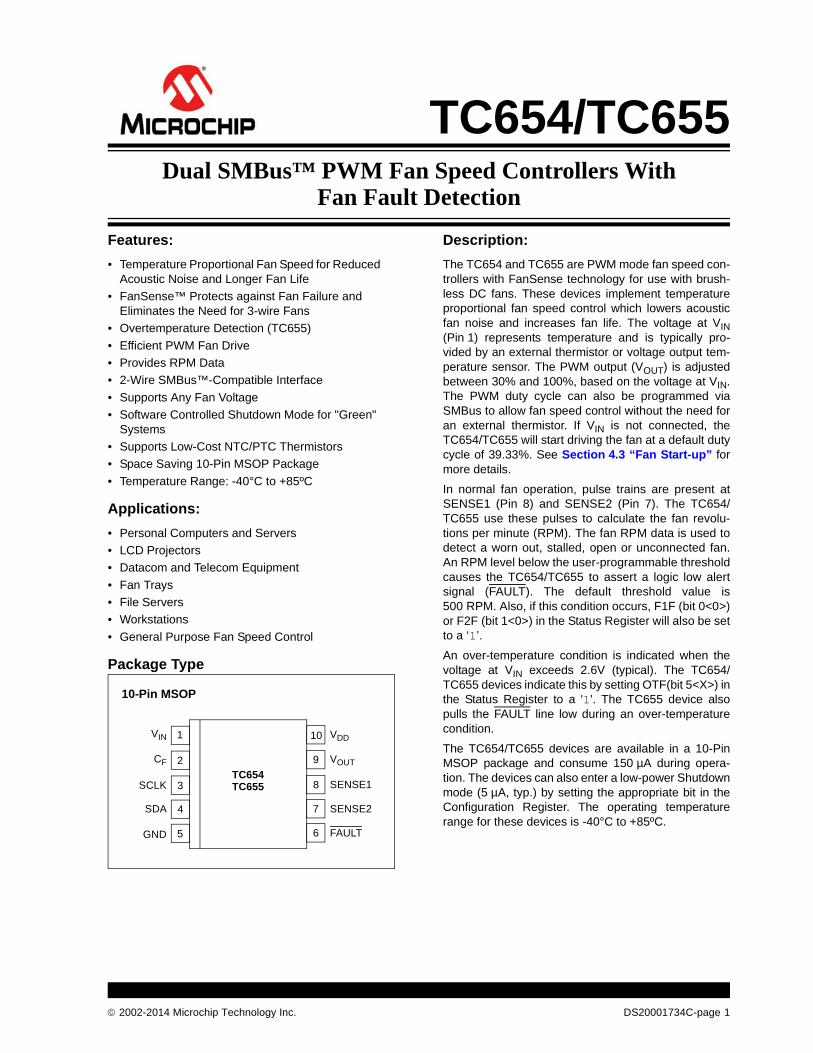
The TC654 and TC655 are PWM mode fan speed con-trollers with FanSense technology for use with brush-less DC fans. These devices implement temperatureproportional fan speed control which lowers acousticfan noise and increases fan life. The voltage at VIN(Pin 1) represents temperature and is typically pro-vided by an external thermistor or voltage output tem-perature sensor. The PWM output (VOUT) is adjustedbetween 30% and 100%, based on the voltage at VIN.The PWM duty cycle can also be programmed viaSMBus to allow fan speed control without the need foran external thermistor. If VIN is not connected, theTC654/TC655 will start driving the fan at a default dutycycle of 39.33%. See Section 4.3 “Fan Start-up” formore details.
In normal fan operation, pulse trains are present atSENSE1 (Pin 8) and SENSE2 (Pin 7). The TC654/TC655 use these pulses to calculate the fan revolu-tions per minute (RPM). The fan RPM data is used todetect a worn out, stalled, open or unconnected fan.An RPM level below the user-programmable thresholdcauses the TC654/TC655 to assert a logic low alertsignal (FAULT). The default threshold value is500 RPM. Also, if this condition occurs, F1F (bit 0<0>)or F2F (bit 1<0>) in the Status Register will also be setto a ‘1’.
An over-temperature condition is indicated when thevoltage at VIN exceeds 2.6V (typical). The TC654/TC655 devices indicate this by setting OTF(bit 5<X>) inthe Status Register to a '1'. The TC655 device alsopulls the FAULT line low during an over-temperaturecondition.
The TC654/TC655 devices are available in a 10-PinMSOP package and consume 150 µA during opera-tion. The devices can also enter a low-power Shutdownmode (5 µA, typ.) by setting the appropriate bit in theConfiguration Register. The operating temperaturerange for these devices is -40°C to +85ºC.
10-Pin MSOP
1
2
3
4
5
10
9
8
7
6
VIN
CF
SCLK
SDA
GND
VDD
VOUT
SENSE1
SENSE2
FAULT
TC654TC655
2002-2014 Microchip Technology Inc. DS20001734C-page 1
TC654/TC655
Functional Block Diagram
VOTF
50 k
OTF
VMIN
TC654/TC655
SENSE1
FAULT
VOUT
VDD
GND
SDA
SCLK
CF
VIN –
+
+
–
ClockGenerator
Serial PortInterface
ControlLogic
Start-upTimer
MissingPulseDetect
100 mV (typ.)
–
50 kSENSE2
100 mV (typ.)
–
–
+
Note: OTF condition applies for the TC655 device only.
Note
DS20001734C-page 2 2002-2014 Microchip Technology Inc.
TC654/TC655
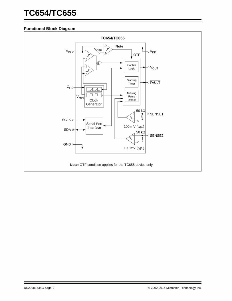
1.0 ELECTRICAL CHARACTERISTICS
Absolute Maximum Ratings *
VDD...................................................................................6.5V
Input Voltages ...................................... -0.3V to (VDD + 0.3V)
Output Voltages .................................... -0.3V to (VDD + 0.3V)
Storage temperature .....................................-65°C to +150°C
Ambient temp. with power applied ................-40°C to +125°C
Maximum Junction Temperature, TJ ............................. 150°C
ESD protection on all pins 4 kV
*Notice: Stresses above those listed under “Maximum rat-ings” may cause permanent damage to the device. This is astress rating only and functional operation of the device atthose or any other conditions above those indicated in theoperational listings of this specification is not implied. Expo-sure to maximum rating conditions for extended periods mayaffect device reliability.
PIN FUNCTION TABLE
Name Function
VIN Analog Input
CF Analog Output
SCLK Serial Clock Input
SDA Serial Data In/Out (Open Drain)
GND Ground
FAULT Digital (Open Drain) Output
SENSE2 Analog Input
SENSE1 Analog Input
VOUT Digital Output
VDD Power Supply Input
ELECTRICAL SPECIFICATIONS
Electrical Characteristics: Unless otherwise noted, all limits are specified for VDD = 3.0V to 5.5V, -40°C <TA < +85°C.
Parameters Sym. Min. Typ. Max. Units Conditions
Supply Voltage VDD 3.0 — 5.5 V
Operating Supply Current IDD — 150 300 µA Pins 7, 8, 9 Open
Shutdown Mode Supply Current IDDSHDN — 5 10 µA Pins 7, 8, 9 Open
VOUT PWM Output
VOUT Rise Time tR — — 50 µsec IOH = 5 mA, Note 1
VOUT Fall Time tF — — 50 µsec IOL = 1 mA, Note 1
Sink Current at VOUT Output IOL 1.0 — — mA VOL = 10% of VDD
Source Current at VOUT Output IOH 5.0 — — mA VOH = 80% of VDD
PWM Frequency F 26 30 34 Hz CF = 1 µF
VIN Input
VIN Input Voltage for 100% PWM duty-cycle
VC(MAX) 2.45 2.6 2.75 V
VC(MAX) - VC(MIN) VCRANGE 1.25 1.4 1.55 V
VIN Input Resistance — 10M — VDD = 5.0V
VIN Input Leakage Current IIN -1.0 — +1.0 µA
SENSE Input
SENSE Input Threshold Voltage with Respect to GND
VTHSENSE 80 100 120 mV
FAULT Output
FAULT Output LOW Voltage VOL — — 0.3 V IOL = 2.5 mA
FAULT Output Response Time tFAULT — 2.4 — sec
Fan RPM-to-Digital Output
Fan RPM ERROR -15 — +15 % RPM > 1600
Note 1: Not production tested, ensured by design, tested during characterization.2: For 5.0V > VDD 5.5V, the limit for VIH = 2.2V.
2002-2014 Microchip Technology Inc. DS20001734C-page 3
TC654/TC655
TEMPERATURE SPECIFICATIONS
TIMING SPECIFICATIONS
2-Wire Serial Bus Interface
Logic Input High VIH 2.1 — — V Note 2
Logic Input Low VIL — — 0.8 V
Logic Output Low VOL — — 0.4 V IOL = 3 mA
Input Capacitance SDA, SCLK CIN — 10 15 pF Note 1
I/O Leakage Current ILEAK -1.0 — +1.0 µA
SDA Output Low Current IOLSDA 6 — — mA VOL = 0.6V
Electrical Characteristics: Unless otherwise noted, all parameters apply at VDD = 3.0 V to 5.5 V
Parameters Symbol Min Typ Max Units Conditions
Temperature Ranges
Specified Temperature Range TA -40 — +85 °C
Operating Temperature Range TA -40 — +125 °C
Storage Temperature Range TA -65 — +150 °C
Thermal Package Resistances
Thermal Resistance, 10 Pin MSOP JA — 113 — °C/W
Electrical Characteristics: Unless otherwise noted, all limits are specified for VDD = 3.0V to 5.5V,-40°C <TA < +85°C
Parameters Sym Min Typ Max Units Conditions
SMBus Interface (See Figure 1-1)
Serial Port Frequency fSC 0 — 100 kHz Note 1
Low Clock Period tLOW 4.7 — — µsec Note 1
High Clock Period tHIGH 4.7 — — µsec Note 1
SCLK and SDA Rise Time tR — — 1000 nsec Note 1
SCLK and SDA Fall Time tF — — 300 nsec Note 1
Start Condition Setup Time tSU(START) 4.7 — — µsec Note 1
SCLK Clock Period Time tSC 10 — — µsec Note 1
Start Condition Hold Time tH(START) 4.0 — — µsec Note 1
Data in SetupTime to SCLK High
tSU-DATA 250 — — nsec Note 1
Data in Hold Time after SCLK Low
tH-DATA 300 — — nsec Note 1
Stop Condition Setup Time tSU(STOP) 4.0 — — µsec Note 1
Bus Free Time Prior to New Transition
tIDLE 4.7 — µsec Note 1 and Note 2
Note 1: Not production tested, ensured by design, tested during characterization.2: Time the bus must be free before a new transmission can start.
ELECTRICAL SPECIFICATIONS (CONTINUED)
Electrical Characteristics: Unless otherwise noted, all limits are specified for VDD = 3.0V to 5.5V, -40°C <TA < +85°C.
Parameters Sym. Min. Typ. Max. Units Conditions
Note 1: Not production tested, ensured by design, tested during characterization.2: For 5.0V > VDD 5.5V, the limit for VIH = 2.2V.
DS20001734C-page 4 2002-2014 Microchip Technology Inc.
TC654/TC655
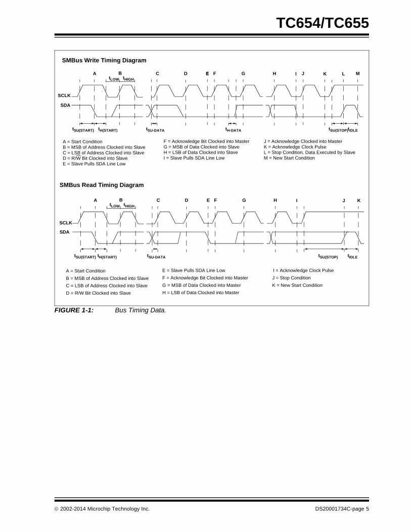
FIGURE 1-1: Bus Timing Data.
tSU(START) tH(START) tSU-DATA tSU(STOP)tIDLE
A = Start Condition B = MSB of Address Clocked into Slave C = LSB of Address Clocked into Slave D = R/W Bit Clocked into Slave E = Slave Pulls SDA Line Low
A B C D E F G H I J K L M
F = Acknowledge Bit Clocked into Master G = MSB of Data Clocked into Slave H = LSB of Data Clocked into Slave I = Slave Pulls SDA Line Low
J = Acknowledge Clocked into Master K = Acknowledge Clock Pulse L = Stop Condition, Data Executed by Slave M = New Start Condition
tLOW tHIGH
SCLK
SDA
tH-DATA
SMBus Write Timing Diagram
tSU(START) tH(START) tSU-DATA tSU(STOP) tIDLE
A = Start Condition
B = MSB of Address Clocked into Slave
C = LSB of Address Clocked into Slave
D = R/W Bit Clocked into Slave
A B C D E F G H I J K
E = Slave Pulls SDA Line Low
F = Acknowledge Bit Clocked into Master
G = MSB of Data Clocked into Master
H = LSB of Data Clocked into Master
tLOW tHIGH
I = Acknowledge Clock Pulse
J = Stop Condition
K = New Start Condition
SCLK
SDA
SMBus Read Timing Diagram
E
2002-2014 Microchip Technology Inc. DS20001734C-page 5
TC654/TC655
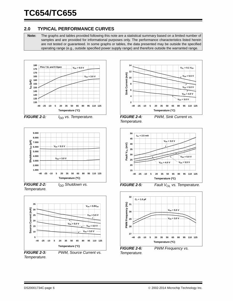
2.0 TYPICAL PERFORMANCE CURVES
FIGURE 2-1: IDD vs. Temperature.
FIGURE 2-2: IDD Shutdown vs. Temperature.
FIGURE 2-3: PWM, Source Current vs. Temperature.
FIGURE 2-4: PWM, Sink Current vs. Temperature.
FIGURE 2-5: Fault VOL vs. Temperature.
FIGURE 2-6: PWM Frequency vs. Temperature.
Note: The graphs and tables provided following this note are a statistical summary based on a limited number ofsamples and are provided for informational purposes only. The performance characteristics listed hereinare not tested or guaranteed. In some graphs or tables, the data presented may be outside the specifiedoperating range (e.g., outside specified power supply range) and therefore outside the warranted range.
130
135
140
145
150
155
160
165
170
175
180
-40 -25 -10 5 20 35 50 65 80 95 110 125
Temperature (°C)
I DD (
µA
)
VDD = 5.5 V
VDD = 3.0 V
Pins 7,8, and 9 Open
1.000
2.000
3.000
4.000
5.000
6.000
7.000
8.000
9.000
-40 -25 -10 5 20 35 50 65 80 95 110 125
Temperature (ºC)
Sh
utd
ow
n I
DD (
µA
)
VDD = 3.0 V
VDD = 5.5 V
5
10
15
20
25
30
35
-40 -25 -10 5 20 35 50 65 80 95 110 125
Temperature (°C)
So
urc
e C
urr
ent
(mA
)
VDD = 5.5 V
VDD = 5.0 VVDD = 4.0 V
VDD = 3.0 V
VOH = 0.8VDD
2
4
6
8
10
12
14
-40 -25 -10 5 20 35 50 65 80 95 110 125
Temperature (°C)
Sin
k C
urr
ent
(mA
)
VDD = 5.5 V
VDD = 5.0 V
VDD = 4.0 V
VDD = 3.0 V
VOL = 0.1 VDD
15
20
25
30
35
40
45
50
-40 -25 -10 5 20 35 50 65 80 95 110 125
Temperature (ºC)
Fau
lt V
OL (
mV
)
IOL = 2.5 mA
VDD = 5.5 V
VDD = 5.0 V
VDD = 4.0 V
VDD = 3.0 V
27
28
29
30
31
32
-40 -25 -10 5 20 35 50 65 80 95 110 125
Temperature (ºC)
PW
M F
req
uen
cy (
Hz)
VDD = 5.5 V
VDD = 3.0 V
CF = 1.0 µF
DS20001734C-page 6 2002-2014 Microchip Technology Inc.
TC654/TC655
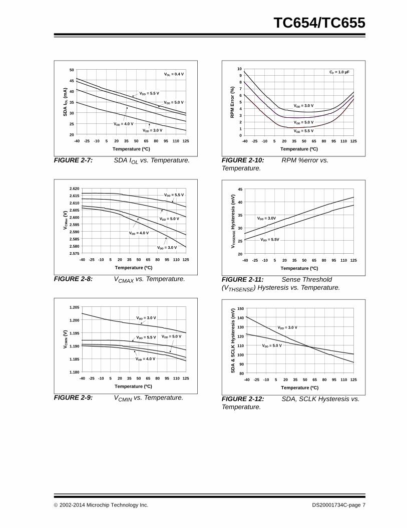
FIGURE 2-7: SDA IOL vs. Temperature.
FIGURE 2-8: VCMAX vs. Temperature.
FIGURE 2-9: VCMIN vs. Temperature.
FIGURE 2-10: RPM %error vs. Temperature.
FIGURE 2-11: Sense Threshold (VTHSENSE) Hysteresis vs. Temperature.
FIGURE 2-12: SDA, SCLK Hysteresis vs. Temperature.
20
25
30
35
40
45
50
-40 -25 -10 5 20 35 50 65 80 95 110 125
Temperature (ºC)
SD
A I O
L (
mA
)
VOL = 0.4 V
VDD = 5.5 V
VDD = 5.0 V
VDD = 4.0 V
VDD = 3.0 V
2.575
2.580
2.585
2.590
2.595
2.600
2.605
2.610
2.615
2.620
-40 -25 -10 5 20 35 50 65 80 95 110 125
Temperature (ºC)
VC
Max
(V
)
VDD = 3.0 V
VDD = 4.0 V
VDD = 5.0 V
VDD = 5.5 V
1.180
1.185
1.190
1.195
1.200
1.205
-40 -25 -10 5 20 35 50 65 80 95 110 125
Temperature (ºC)
VC
MIN
(V
)
VDD = 3.0 V
VDD = 5.0 VVDD = 5.5 V
VDD = 4.0 V
0
1
2
3
4
5
6
7
8
9
10
-40 -25 -10 5 20 35 50 65 80 95 110 125
Temperature (ºC)
RP
M E
rro
r (%
)
VDD = 3.0 V
VDD = 5.5 V
VDD = 5.0 V
CF = 1.0 µF
20
25
30
35
40
45
-40 -25 -10 5 20 35 50 65 80 95 110 125
Temperature (ºC)
VT
HS
EN
SE H
yste
resi
s (m
V)
VDD = 3.0V
VDD = 5.5V
80
90
100
110
120
130
140
150
-40 -25 -10 5 20 35 50 65 80 95 110 125
Temperature (ºC)
SD
A &
SC
LK
Hys
tere
sis
(mV
)
VDD = 3.0 V
VDD = 5.0 V
2002-2014 Microchip Technology Inc. DS20001734C-page 7
TC654/TC655
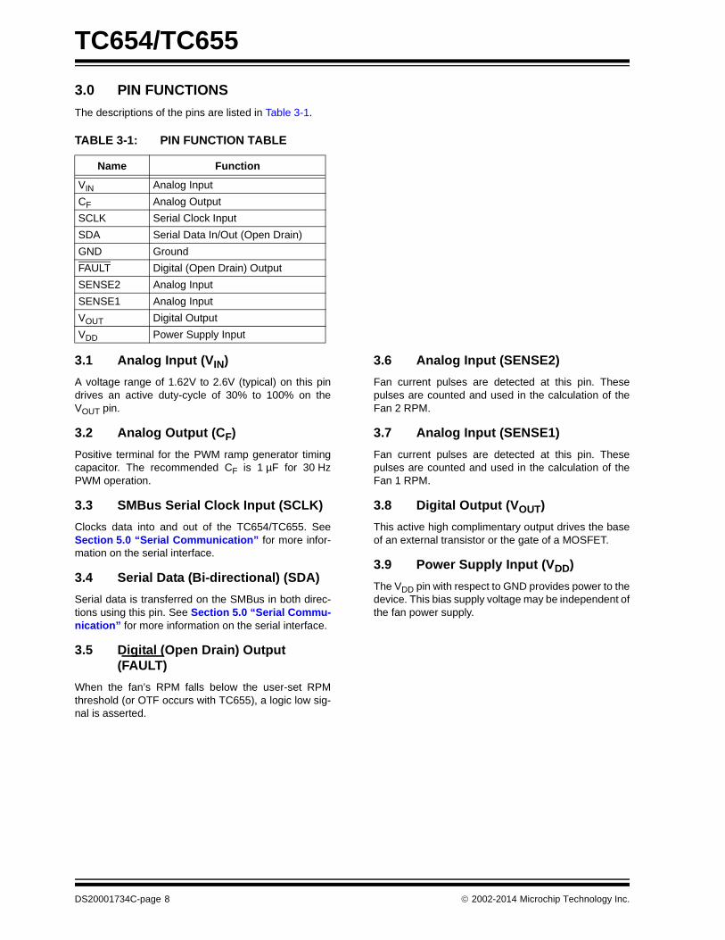
3.0 PIN FUNCTIONS
The descriptions of the pins are listed in Table 3-1.
TABLE 3-1: PIN FUNCTION TABLE
3.1 Analog Input (VIN)
A voltage range of 1.62V to 2.6V (typical) on this pindrives an active duty-cycle of 30% to 100% on theVOUT pin.
3.2 Analog Output (CF)
Positive terminal for the PWM ramp generator timingcapacitor. The recommended CF is 1 µF for 30 HzPWM operation.
3.3 SMBus Serial Clock Input (SCLK)
Clocks data into and out of the TC654/TC655. SeeSection 5.0 “Serial Communication” for more infor-mation on the serial interface.
3.4 Serial Data (Bi-directional) (SDA)
Serial data is transferred on the SMBus in both direc-tions using this pin. See Section 5.0 “Serial Commu-nication” for more information on the serial interface.
3.5 Digital (Open Drain) Output (FAULT)
When the fan’s RPM falls below the user-set RPMthreshold (or OTF occurs with TC655), a logic low sig-nal is asserted.
3.6 Analog Input (SENSE2)
Fan current pulses are detected at this pin. Thesepulses are counted and used in the calculation of theFan 2 RPM.
3.7 Analog Input (SENSE1)
Fan current pulses are detected at this pin. Thesepulses are counted and used in the calculation of theFan 1 RPM.
3.8 Digital Output (VOUT)
This active high complimentary output drives the baseof an external transistor or the gate of a MOSFET.
3.9 Power Supply Input (VDD)
The VDD pin with respect to GND provides power to thedevice. This bias supply voltage may be independent ofthe fan power supply.
Name Function
VIN Analog Input
CF Analog Output
SCLK Serial Clock Input
SDA Serial Data In/Out (Open Drain)
GND Ground
FAULT Digital (Open Drain) Output
SENSE2 Analog Input
SENSE1 Analog Input
VOUT Digital Output
VDD Power Supply Input
DS20001734C-page 8 2002-2014 Microchip Technology Inc.
TC654/TC655
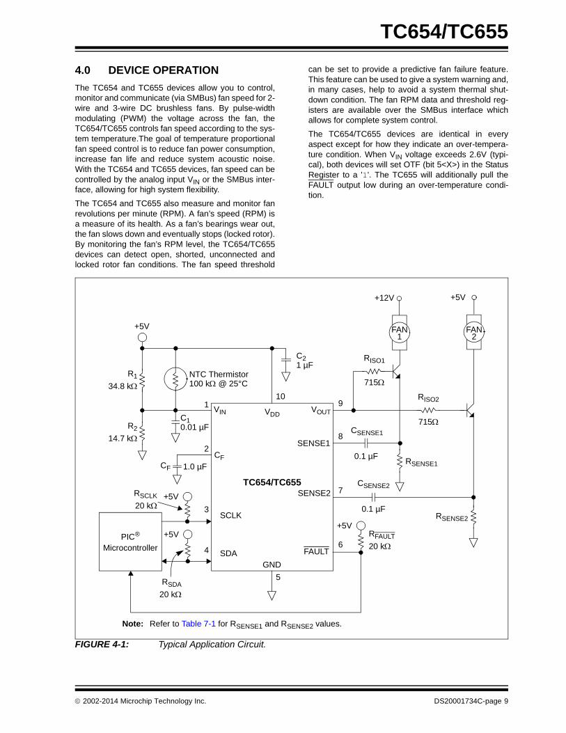
4.0 DEVICE OPERATION
The TC654 and TC655 devices allow you to control,monitor and communicate (via SMBus) fan speed for 2-wire and 3-wire DC brushless fans. By pulse-widthmodulating (PWM) the voltage across the fan, theTC654/TC655 controls fan speed according to the sys-tem temperature.The goal of temperature proportionalfan speed control is to reduce fan power consumption,increase fan life and reduce system acoustic noise.With the TC654 and TC655 devices, fan speed can becontrolled by the analog input VIN or the SMBus inter-face, allowing for high system flexibility.
The TC654 and TC655 also measure and monitor fanrevolutions per minute (RPM). A fan’s speed (RPM) isa measure of its health. As a fan’s bearings wear out,the fan slows down and eventually stops (locked rotor).By monitoring the fan’s RPM level, the TC654/TC655devices can detect open, shorted, unconnected andlocked rotor fan conditions. The fan speed threshold
can be set to provide a predictive fan failure feature.This feature can be used to give a system warning and,in many cases, help to avoid a system thermal shut-down condition. The fan RPM data and threshold reg-isters are available over the SMBus interface whichallows for complete system control.
The TC654/TC655 devices are identical in everyaspect except for how they indicate an over-tempera-ture condition. When VIN voltage exceeds 2.6V (typi-cal), both devices will set OTF (bit 5<X>) in the StatusRegister to a '1'. The TC655 will additionally pull theFAULT output low during an over-temperature condi-tion.
FIGURE 4-1: Typical Application Circuit.
1
2
3
4
5
6
7
8
910
VIN
CF
SCLK
SDAGND
FAULT
SENSE2
SENSE1
VOUTVDD
+5V FAN FAN
RISO1
RISO2
RSENSE2
RSENSE1
CSENSE2
CSENSE1
1 2
NTC ThermistorR1
R2
C10.01 µF
C21 µF
100 k @ 25°C
PIC®
Microcontroller
+12V +5V
+5V
+5V+5V
34.8 k
14.7 k
CF 1.0 µF
RSCLK
20 k
RSDA
20 k
715
0.1 µF
0.1 µF
715
RFAULT
20 k
Note: Refer to Table 7-1 for RSENSE1 and RSENSE2 values.
TC654/TC655
2002-2014 Microchip Technology Inc. DS20001734C-page 9
TC654/TC655
4.1 Fan Speed Control Methods
The speed of a DC brushless fan is proportional to thevoltage across it. For example, if a fan’s rating is5000 RPM at 12V, it’s speed would be 2500 RPM at 6V.This, of course, will not be exact, but should be close.
There are two main methods for fan speed control. Thefirst is pulse width modulation (PWM) and the secondis linear. Using either method the total system powerrequirement to run the fan is equal. The differencebetween the two methods is where the power isconsumed.
The following example compares the two methods fora 12V, 120 mA fan running at 50% speed. With 6Vapplied across the fan, the fan draws an average cur-rent of 68 mA. Using a linear control method, there are6V across the fan and 6V across the drive element.With 6V and 68 mA, the drive element is dissipating410 mW of power. Using the PWM approach, the fan ismodulated at a 50% duty cycle, with most of the 12Vbeing dropped across the fan. With 50% duty cycle, thefan draws an RMS current of 110 mA and an averagecurrent of 72 mA. Using a MOSFET with a 1 RDS(on)(a fairly typical value for this low current) the power dis-sipation in the drive element would be: 12 mW (Irms2 *RDS(on)). Using a standard 2N2222A NPN transistor(assuming a Vce-sat of 0.8V), the power dissipationwould be 58 mW (Iavg* Vce-sat).
The PWM approach to fan speed control causes muchless power dissipation in the drive element. This allowssmaller devices to be used and will not require any spe-cial heatsinking to get rid of the power being dissipatedin the package.
The other advantage to the PWM approach is that thevoltage being applied to the fan is always near 12V.This eliminates any concern about not supplying a highenough voltage to run the internal fan components,which is very relevant in linear fan speed control.
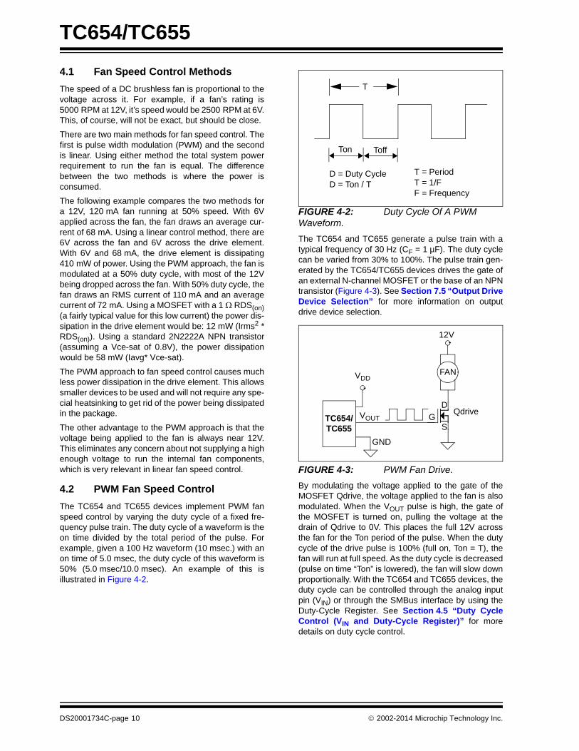
4.2 PWM Fan Speed Control
The TC654 and TC655 devices implement PWM fanspeed control by varying the duty cycle of a fixed fre-quency pulse train. The duty cycle of a waveform is theon time divided by the total period of the pulse. Forexample, given a 100 Hz waveform (10 msec.) with anon time of 5.0 msec, the duty cycle of this waveform is50% (5.0 msec/10.0 msec). An example of this isillustrated in Figure 4-2.
FIGURE 4-2: Duty Cycle Of A PWM Waveform.
The TC654 and TC655 generate a pulse train with atypical frequency of 30 Hz (CF = 1 µF). The duty cyclecan be varied from 30% to 100%. The pulse train gen-erated by the TC654/TC655 devices drives the gate ofan external N-channel MOSFET or the base of an NPNtransistor (Figure 4-3). See Section 7.5 “Output DriveDevice Selection” for more information on outputdrive device selection.
FIGURE 4-3: PWM Fan Drive.
By modulating the voltage applied to the gate of theMOSFET Qdrive, the voltage applied to the fan is alsomodulated. When the VOUT pulse is high, the gate ofthe MOSFET is turned on, pulling the voltage at thedrain of Qdrive to 0V. This places the full 12V acrossthe fan for the Ton period of the pulse. When the dutycycle of the drive pulse is 100% (full on, Ton = T), thefan will run at full speed. As the duty cycle is decreased(pulse on time “Ton” is lowered), the fan will slow downproportionally. With the TC654 and TC655 devices, theduty cycle can be controlled through the analog inputpin (VIN) or through the SMBus interface by using theDuty-Cycle Register. See Section 4.5 “Duty CycleControl (VIN and Duty-Cycle Register)” for moredetails on duty cycle control.
T
Ton Toff
T = PeriodT = 1/FF = Frequency
D = Duty CycleD = Ton / T
TC654/TC655
FAN
12V
Qdrive
VDD
GND
VOUT G
D
S
DS20001734C-page 10 2002-2014 Microchip Technology Inc.
TC654/TC655
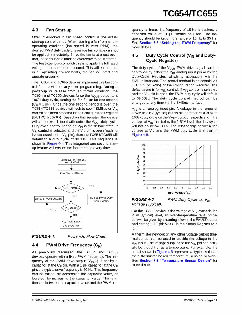
4.3 Fan Start-up
Often overlooked in fan speed control is the actualstart-up control period. When starting a fan from a non-operating condition (fan speed is zero RPM), thedesired PWM duty cycle or average fan voltage can notbe applied immediately. Since the fan is at a rest posi-tion, the fan’s inertia must be overcome to get it started.The best way to accomplish this is to apply the full ratedvoltage to the fan for one second. This will ensure thatin all operating environments, the fan will start andoperate properly.
The TC654 and TC655 devices implement this fan con-trol feature without any user programming. During apower-up or release from shutdown condition, theTC654 and TC655 devices force the VOUT output to a100% duty cycle, turning the fan full on for one second(CF = 1 µF). Once the one second period is over, theTC654/TC655 devices will look to see if SMBus or VINcontrol has been selected in the Configuration Register(DUTYC bit 5<0>). Based on this register, the devicewill choose which input will control the VOUT duty cycle.Duty cycle control based on VIN is the default state. IfVIN control is selected and the VIN pin is open (nothingis connected to the VIN pin), then the TC654/TC655 willdefault to a duty cycle of 39.33%. This sequence isshown in Figure 4-4. This integrated one second start-up feature will ensure the fan starts-up every time.
FIGURE 4-4: Power-Up Flow Chart.
4.4 PWM Drive Frequency (CF)
As previously discussed, the TC654 and TC655devices operate with a fixed PWM frequency. The fre-quency of the PWM drive output (VOUT) is set by acapacitor at the CF pin. With a 1 µF capacitor at the CFpin, the typical drive frequency is 30 Hz. This frequencycan be raised, by decreasing the capacitor value, orlowered, by increasing the capacitor value. The rela-tionship between the capacitor value and the PWM fre-
quency is linear. If a frequency of 15 Hz is desired, acapacitor value of 2.0 µF should be used. The fre-quency should be kept in the range of 15 Hz to 35 Hz.See Section 7.2 “Setting the PWM Frequency” formore details.
4.5 Duty Cycle Control (VIN and Duty-Cycle Register)
The duty cycle of the VOUT PWM drive signal can becontrolled by either the VIN analog input pin or by theDuty-Cycle Register, which is accessible via theSMBus interface. The control method is selectable viaDUTYC (bit 5<0>) of the Configuration Register. Thedefault state is for VIN control. If VIN control is selectedand the VIN pin is open, the PWM duty cycle will defaultto 39.33%. The duty cycle control method can bechanged at any time via the SMBus interface.
VIN is an analog input pin. A voltage in the range of1.62V to 2.6V (typical) at this pin commands a 30% to100% duty cycle on the VOUT output, respectively. If thevoltage at VIN falls below the 1.62V level, the duty cyclewill not go below 30%. The relationship between thevoltage at VIN and the PWM duty cycle is shown inFigure 4-5.
FIGURE 4-5: PWM Duty Cycle vs. VIN Voltage (Typical).
For the TC655 device, if the voltage at VIN exceeds the2.6V (typical) level, an over-temperature fault indica-tion will be given by asserting a low at the FAULT outputand setting OTF (bit 5<X>) in the Status Register to a‘1’.
A thermistor network or any other voltage output ther-mal sensor can be used to provide the voltage to theVIN input. The voltage supplied to the VIN pin can actu-ally be thought of as a temperature. For example, thecircuit shown in Figure 4-6 represents a typical solutionfor a thermistor based temperature sensing network.See Section 7.3 “Temperature Sensor Design” formore details.
Power-Up or Release from SHDN
One Second Pulse
Select SMBus
NO
VIN Open?
NO
YES
YES
Default PWM: 39.33% SMBus PWM DutyCycle Control
VIN PWM Duty
Cycle Control
0
10
20
30
40
50
60
70
80
90
100
1 1.2 1.4 1.6 1.8 2 2.2 2.4 2.6 2.8
Input Voltage (VIN)
Du
ty C
ycle
(%
)
2002-2014 Microchip Technology Inc. DS20001734C-page 11
TC654/TC655
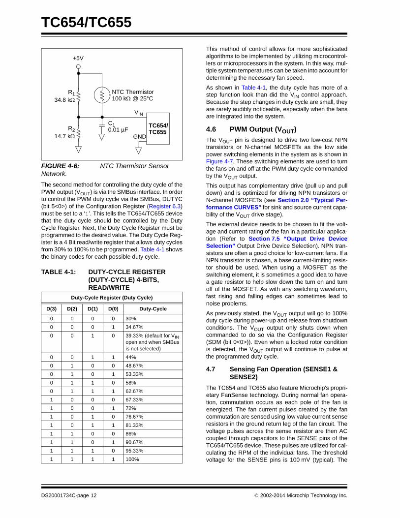
FIGURE 4-6: NTC Thermistor Sensor Network.
The second method for controlling the duty cycle of thePWM output (VOUT) is via the SMBus interface. In orderto control the PWM duty cycle via the SMBus, DUTYC(bit 5<0>) of the Configuration Register (Register 6.3)must be set to a ‘1’. This tells the TC654/TC655 devicethat the duty cycle should be controlled by the DutyCycle Register. Next, the Duty Cycle Register must beprogrammed to the desired value. The Duty Cycle Reg-ister is a 4 Bit read/write register that allows duty cyclesfrom 30% to 100% to be programmed. Table 4-1 showsthe binary codes for each possible duty cycle.
TABLE 4-1: DUTY-CYCLE REGISTER (DUTY-CYCLE) 4-BITS,READ/WRITE
This method of control allows for more sophisticatedalgorithms to be implemented by utilizing microcontrol-lers or microprocessors in the system. In this way, mul-tiple system temperatures can be taken into account fordetermining the necessary fan speed.
As shown in Table 4-1, the duty cycle has more of astep function look than did the VIN control approach.Because the step changes in duty cycle are small, theyare rarely audibly noticeable, especially when the fansare integrated into the system.
4.6 PWM Output (VOUT)
The VOUT pin is designed to drive two low-cost NPNtransistors or N-channel MOSFETs as the low sidepower switching elements in the system as is shown inFigure 4-7. These switching elements are used to turnthe fans on and off at the PWM duty cycle commandedby the VOUT output.
This output has complementary drive (pull up and pulldown) and is optimized for driving NPN transistors orN-channel MOSFETs (see Section 2.0 “Typical Per-formance CURVES” for sink and source current capa-bility of the VOUT drive stage).
The external device needs to be chosen to fit the volt-age and current rating of the fan in a particular applica-tion (Refer to Section 7.5 “Output Drive DeviceSelection” Output Drive Device Selection). NPN tran-sistors are often a good choice for low-current fans. If aNPN transistor is chosen, a base current-limiting resis-tor should be used. When using a MOSFET as theswitching element, it is sometimes a good idea to havea gate resistor to help slow down the turn on and turnoff of the MOSFET. As with any switching waveform,fast rising and falling edges can sometimes lead tonoise problems.
As previously stated, the VOUT output will go to 100%duty cycle during power-up and release from shutdownconditions. The VOUT output only shuts down whencommanded to do so via the Configuration Register(SDM (bit 0<0>)). Even when a locked rotor conditionis detected, the VOUT output will continue to pulse atthe programmed duty cycle.
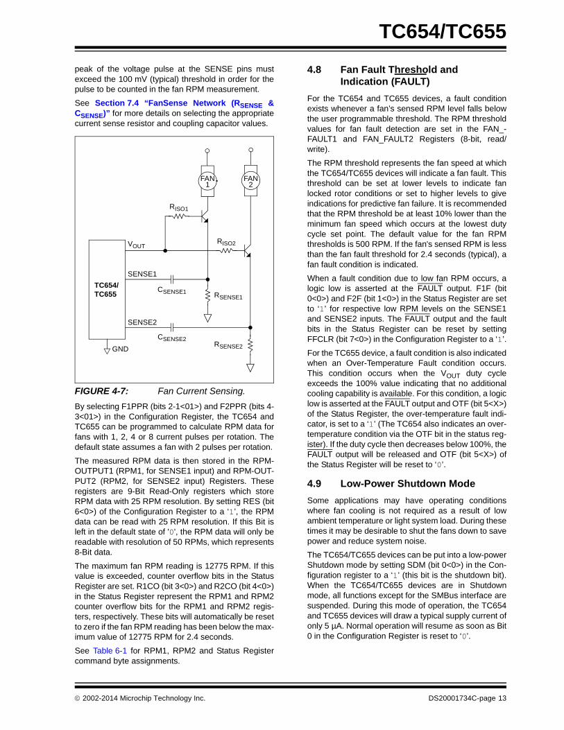
4.7 Sensing Fan Operation (SENSE1 & SENSE2)
The TC654 and TC655 also feature Microchip's propri-etary FanSense technology. During normal fan opera-tion, commutation occurs as each pole of the fan isenergized. The fan current pulses created by the fancommutation are sensed using low value current senseresistors in the ground return leg of the fan circuit. Thevoltage pulses across the sense resistor are then ACcoupled through capacitors to the SENSE pins of theTC654/TC655 device. These pulses are utilized for cal-culating the RPM of the individual fans. The thresholdvoltage for the SENSE pins is 100 mV (typical). The
Duty-Cycle Register (Duty Cycle)
D(3) D(2) D(1) D(0) Duty-Cycle
0 0 0 0 30%
0 0 0 1 34.67%
0 0 1 0 39.33% (default for VIN open and when SMBus is not selected)
0 0 1 1 44%
0 1 0 0 48.67%
0 1 0 1 53.33%
0 1 1 0 58%
0 1 1 1 62.67%
1 0 0 0 67.33%
1 0 0 1 72%
1 0 1 0 76.67%
1 0 1 1 81.33%
1 1 0 0 86%
1 1 0 1 90.67%
1 1 1 0 95.33%
1 1 1 1 100%
VIN
+5V
NTC ThermistorR1
R2
C10.01 µF
100 k @ 25°C
TC654/TC655
GND
34.8 k
14.7 k
DS20001734C-page 12 2002-2014 Microchip Technology Inc.
TC654/TC655
peak of the voltage pulse at the SENSE pins mustexceed the 100 mV (typical) threshold in order for thepulse to be counted in the fan RPM measurement.
See Section 7.4 “FanSense Network (RSENSE &CSENSE)” for more details on selecting the appropriatecurrent sense resistor and coupling capacitor values.
FIGURE 4-7: Fan Current Sensing.
By selecting F1PPR (bits 2-1<01>) and F2PPR (bits 4-3<01>) in the Configuration Register, the TC654 andTC655 can be programmed to calculate RPM data forfans with 1, 2, 4 or 8 current pulses per rotation. Thedefault state assumes a fan with 2 pulses per rotation.
The measured RPM data is then stored in the RPM-OUTPUT1 (RPM1, for SENSE1 input) and RPM-OUT-PUT2 (RPM2, for SENSE2 input) Registers. Theseregisters are 9-Bit Read-Only registers which storeRPM data with 25 RPM resolution. By setting RES (bit6<0>) of the Configuration Register to a ‘1’, the RPMdata can be read with 25 RPM resolution. If this Bit isleft in the default state of '0', the RPM data will only bereadable with resolution of 50 RPMs, which represents8-Bit data.
The maximum fan RPM reading is 12775 RPM. If thisvalue is exceeded, counter overflow bits in the StatusRegister are set. R1CO (bit 3<0>) and R2CO (bit 4<0>)in the Status Register represent the RPM1 and RPM2counter overflow bits for the RPM1 and RPM2 regis-ters, respectively. These bits will automatically be resetto zero if the fan RPM reading has been below the max-imum value of 12775 RPM for 2.4 seconds.
See Table 6-1 for RPM1, RPM2 and Status Registercommand byte assignments.
4.8 Fan Fault Threshold and Indication (FAULT)
For the TC654 and TC655 devices, a fault conditionexists whenever a fan’s sensed RPM level falls belowthe user programmable threshold. The RPM thresholdvalues for fan fault detection are set in the FAN_-FAULT1 and FAN_FAULT2 Registers (8-bit, read/write).
The RPM threshold represents the fan speed at whichthe TC654/TC655 devices will indicate a fan fault. Thisthreshold can be set at lower levels to indicate fanlocked rotor conditions or set to higher levels to giveindications for predictive fan failure. It is recommendedthat the RPM threshold be at least 10% lower than theminimum fan speed which occurs at the lowest dutycycle set point. The default value for the fan RPMthresholds is 500 RPM. If the fan's sensed RPM is lessthan the fan fault threshold for 2.4 seconds (typical), afan fault condition is indicated.
When a fault condition due to low fan RPM occurs, alogic low is asserted at the FAULT output. F1F (bit0<0>) and F2F (bit 1<0>) in the Status Register are setto ‘1’ for respective low RPM levels on the SENSE1and SENSE2 inputs. The FAULT output and the faultbits in the Status Register can be reset by settingFFCLR (bit 7<0>) in the Configuration Register to a ‘1’.
For the TC655 device, a fault condition is also indicatedwhen an Over-Temperature Fault condition occurs.This condition occurs when the VOUT duty cycleexceeds the 100% value indicating that no additionalcooling capability is available. For this condition, a logiclow is asserted at the FAULT output and OTF (bit 5<X>)of the Status Register, the over-temperature fault indi-cator, is set to a ‘1’ (The TC654 also indicates an over-temperature condition via the OTF bit in the status reg-ister). If the duty cycle then decreases below 100%, theFAULT output will be released and OTF (bit 5<X>) ofthe Status Register will be reset to ‘0’.
4.9 Low-Power Shutdown Mode
Some applications may have operating conditionswhere fan cooling is not required as a result of lowambient temperature or light system load. During thesetimes it may be desirable to shut the fans down to savepower and reduce system noise.
The TC654/TC655 devices can be put into a low-powerShutdown mode by setting SDM (bit 0<0>) in the Con-figuration register to a ‘1’ (this bit is the shutdown bit).When the TC654/TC655 devices are in Shutdownmode, all functions except for the SMBus interface aresuspended. During this mode of operation, the TC654and TC655 devices will draw a typical supply current ofonly 5 µA. Normal operation will resume as soon as Bit0 in the Configuration Register is reset to ‘0’.
SENSE2
SENSE1
VOUT
FAN FAN
RISO1
RISO2
RSENSE2
RSENSE1
CSENSE2
CSENSE1
1 2
TC654/TC655
GND
2002-2014 Microchip Technology Inc. DS20001734C-page 13
TC654/TC655
When the TC654/TC655 devices are brought out of aShutdown mode by resetting SDM (bit 0<0>) in theConfiguration Register, all of the registers (except forthe Configuration and FAN_FAULT1 and 2 registers)assume their default power-up states. The Configura-tion Register and the FAN_FAULT1 and 2 Registersmaintain the states they were in prior to the devicebeing put into the Shutdown mode. Since these are theregisters which control the parts operation, the partdoes not have to be reprogrammed for operation whenit comes out of Shutdown mode.
4.10 SMBus Interface (SCLK & SDA)
The TC654/TC655 feature an industry-standard, 2-wireserial interface with factory-set addresses. By commu-nicating with the TC654/TC655 device registers, func-tions like PWM duty cycle, low-power Shutdown modeand fan RPM threshold can be controlled. Critical infor-mation, such as fan fault, over-temperature and fanRPM, can also be obtained via the device data regis-ters. The available data and control registers make theTC654/TC655 devices very flexible and easy to use. Allof the available registers are detailed in Section 6.0“Register Set”.
4.11 SMBus Slave Address
The slave address of the TC654/TC655 is 0011 011and is fixed. This address is different from industry-standard digital temperature sensors (like TCN75) and,therefore, allows the TC654/TC655 to be utilized insystems in conjunction with these components. Pleasecontact Microchip Technology Inc. if alternateaddresses are required.
DS20001734C-page 14 2002-2014 Microchip Technology Inc.
TC654/TC655
5.0 SERIAL COMMUNICATION
5.1 SMBus 2-Wire Interface
The Serial Clock Input (SCLK) and the bi-directionaldata port (SDA) form a 2-wire bi-directional serial portfor communicating with the TC654/TC655. The follow-ing bus protocols have been defined:
• Data transfer may be initiated only when the bus is not busy.
• During data transfer, the data line must remain stable whenever the clock line is high. Changes in the data line while the clock line is high will be interpreted as a Start or Stop condition.
Accordingly, the following Serial Bus conventions havebeen defined.
TABLE 5-1: TC654/TC655 SERIAL BUS CONVENTIONS
5.1.1 DATA TRANSFER
The TC654/TC655 support a bi-directional 2-Wire busand data transmission protocol. The serial protocolsequencing is illustrated in Figure 1-1. Data transfers
are initiated by a Start condition (Start), followed by adevice address byte and one or more data bytes. Thedevice address byte includes a Read/Write selectionbit. Each access must be terminated by a Stop Condi-tion (Stop). A convention call Acknowledge (ACK) con-firms the receipt of each byte. Note that SDA can onlychange during periods when SCLK is low (SDAchanges while SCLK is high are reserved for Start andStop conditions). All bytes are transferred MSB (mostsignificant bit) first.
5.1.2 MASTER/SLAVE
The device that sends data onto the bus is the transmit-ter and the device receiving data is the receiver. Thebus is controlled by a master device which generatesthe serial clock (SCLK), controls the bus access andgenerates the Start and Stop conditions. The TC654/TC655 always work as a slave device. Both master andslave devices can operate as either transmitter orreceiver, but the master device determines which modeis activated.
5.1.3 START CONDITION (START)
A high-to-low transition of the SDA line while the clock(SCLK) is high determines a Start condition. All com-mands must be preceded by a Start condition.
5.1.4 ADDRESS BYTE
Immediately following the Start Condition, the hostmust transmit the address byte to the TC654/TC655.The 7-bit SMBus address for the TC654/TC655 is0011 011. The 7-bit address transmitted in the serialbit stream must match for the TC654/TC655 to respondwith an Acknowledge (indicating the TC654/TC655 ison the bus and ready to accept data). The eighth bit inthe Address Byte is a Read-Write Bit. This bit is a ‘1’ fora read operation or ‘0’ for a write operation. During thefirst phase of any transfer, this bit will be set = 0 to indi-cate that the command byte is being written.
5.1.5 STOP CONDITION (STOP)
A low-to-high transition of the SDA line while the clock(SCLK) is high determines a Stop condition. All opera-tions must be ended with a Stop condition.
5.1.6 DATA VALID
The state of the data line represents valid data when,after a Start condition, the data line is stable for theduration of the high period of the clock signal.
The data on the line must be changed during the lowperiod of the clock signal. There is one clock pulse perbit of data. Each data transfer is initiated with a Startcondition and terminated with a Stop condition. Thenumber of the data bytes transferred between the Startand Stop conditions is determined by the master deviceand is unlimited.
Term Description
Transmitter The device sending data to the bus.
Receiver The device receiving data from the bus.
Master The device which controls the bus: ini-tiating transfers (Start), generating the clock and terminating transfers (Stop).
Slave The device addressed by the master.
Start A unique condition signaling the beginning of a transfer indicated by SDA falling (High to Low) while SCLK is high.
Stop A unique condition signaling the end of a transfer indicated by SDA rising (Low to High) while SCLK is high.
ACK A Receiver acknowledges the receipt of each byte with this unique condi-tion. The Receiver pulls SDA low during SCLK high of the ACK clock-pulse. The Master provides the clock pulse for the ACK cycle.
Busy Communication is not possible because the bus is in use.
NOT Busy When the bus is idle, both SDA and SCLK will remain high.
Data Valid The state of SDA must remain stable during the high period of SCLK in order for a data bit to be considered valid. SDA only changes state while SCLK is low during normal data trans-fers. (See Start and Stop conditions)
2002-2014 Microchip Technology Inc. DS20001734C-page 15
TC654/TC655
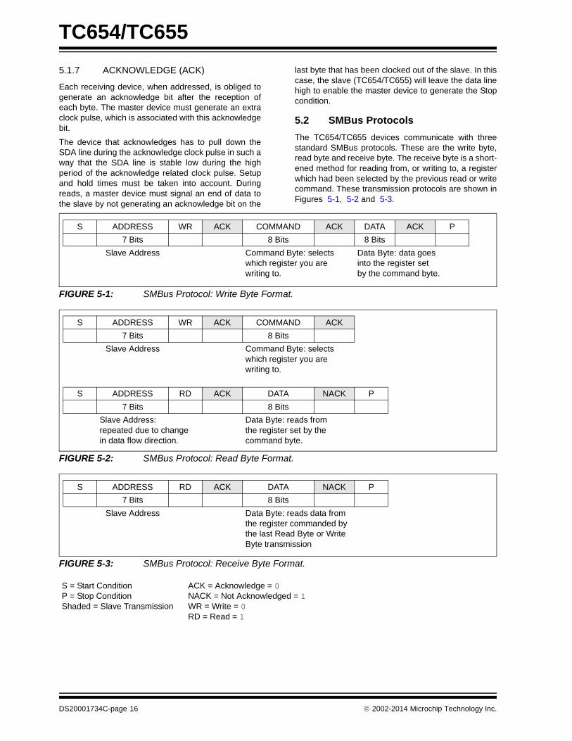
5.1.7 ACKNOWLEDGE (ACK)
Each receiving device, when addressed, is obliged togenerate an acknowledge bit after the reception ofeach byte. The master device must generate an extraclock pulse, which is associated with this acknowledgebit.
The device that acknowledges has to pull down theSDA line during the acknowledge clock pulse in such away that the SDA line is stable low during the highperiod of the acknowledge related clock pulse. Setupand hold times must be taken into account. Duringreads, a master device must signal an end of data tothe slave by not generating an acknowledge bit on the
last byte that has been clocked out of the slave. In thiscase, the slave (TC654/TC655) will leave the data linehigh to enable the master device to generate the Stopcondition.
5.2 SMBus Protocols
The TC654/TC655 devices communicate with threestandard SMBus protocols. These are the write byte,read byte and receive byte. The receive byte is a short-ened method for reading from, or writing to, a registerwhich had been selected by the previous read or writecommand. These transmission protocols are shown inFigures 5-1, 5-2 and 5-3.
FIGURE 5-1: SMBus Protocol: Write Byte Format.
FIGURE 5-2: SMBus Protocol: Read Byte Format.
FIGURE 5-3: SMBus Protocol: Receive Byte Format.
S ADDRESS WR ACK COMMAND ACK DATA ACK P
7 Bits 8 Bits 8 Bits
Slave Address Command Byte: selects which register you arewriting to.
Data Byte: data goesinto the register setby the command byte.
S ADDRESS WR ACK COMMAND ACK
7 Bits 8 Bits
Slave Address Command Byte: selects which register you arewriting to.
S ADDRESS RD ACK DATA NACK P
7 Bits 8 Bits
Slave Address:repeated due to changein data flow direction.
Data Byte: reads fromthe register set by thecommand byte.
S ADDRESS RD ACK DATA NACK P
7 Bits 8 Bits
Slave Address Data Byte: reads data fromthe register commanded bythe last Read Byte or WriteByte transmission
S = Start ConditionP = Stop ConditionShaded = Slave Transmission
ACK = Acknowledge = 0NACK = Not Acknowledged = 1WR = Write = 0RD = Read = 1
DS20001734C-page 16 2002-2014 Microchip Technology Inc.
TC654/TC655
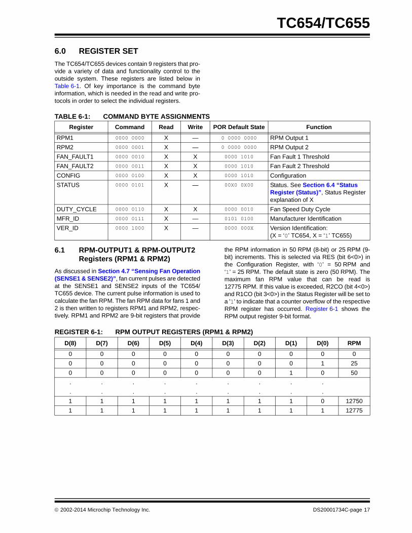
6.0 REGISTER SET
The TC654/TC655 devices contain 9 registers that pro-vide a variety of data and functionality control to theoutside system. These registers are listed below inTable 6-1. Of key importance is the command byteinformation, which is needed in the read and write pro-tocols in order to select the individual registers.
TABLE 6-1: COMMAND BYTE ASSIGNMENTS
6.1 RPM-OUTPUT1 & RPM-OUTPUT2 Registers (RPM1 & RPM2)
As discussed in Section 4.7 “Sensing Fan Operation(SENSE1 & SENSE2)”, fan current pulses are detectedat the SENSE1 and SENSE2 inputs of the TC654/TC655 device. The current pulse information is used tocalculate the fan RPM. The fan RPM data for fans 1 and2 is then written to registers RPM1 and RPM2, respec-tively. RPM1 and RPM2 are 9-bit registers that provide
the RPM information in 50 RPM (8-bit) or 25 RPM (9-bit) increments. This is selected via RES (bit 6<0>) inthe Configuration Register, with ‘0’ = 50 RPM and‘1’ = 25 RPM. The default state is zero (50 RPM). Themaximum fan RPM value that can be read is12775 RPM. If this value is exceeded, R2CO (bit 4<0>)and R1CO (bit 3<0>) in the Status Register will be set toa '1' to indicate that a counter overflow of the respectiveRPM register has occurred. Register 6-1 shows theRPM output register 9-bit format.
REGISTER 6-1: RPM OUTPUT REGISTERS (RPM1 & RPM2)
Register Command Read Write POR Default State Function
RPM1 0000 0000 X — 0 0000 0000 RPM Output 1
RPM2 0000 0001 X — 0 0000 0000 RPM Output 2
FAN_FAULT1 0000 0010 X X 0000 1010 Fan Fault 1 Threshold
FAN_FAULT2 0000 0011 X X 0000 1010 Fan Fault 2 Threshold
CONFIG 0000 0100 X X 0000 1010 Configuration
STATUS 0000 0101 X — 00X0 0X00 Status. See Section 6.4 “Status Register (Status)”, Status Register explanation of X
DUTY_CYCLE 0000 0110 X X 0000 0010 Fan Speed Duty Cycle
MFR_ID 0000 0111 X — 0101 0100 Manufacturer Identification
VER_ID 0000 1000 X — 0000 000X Version Identification: (X = ‘0’ TC654, X = ‘1’ TC655)
D(8) D(7) D(6) D(5) D(4) D(3) D(2) D(1) D(0) RPM
0 0 0 0 0 0 0 0 0 0
0 0 0 0 0 0 0 0 1 25
0 0 0 0 0 0 0 1 0 50
. . . . . . . . .
. . . . . . . . .
1 1 1 1 1 1 1 1 0 12750
1 1 1 1 1 1 1 1 1 12775
2002-2014 Microchip Technology Inc. DS20001734C-page 17
TC654/TC655
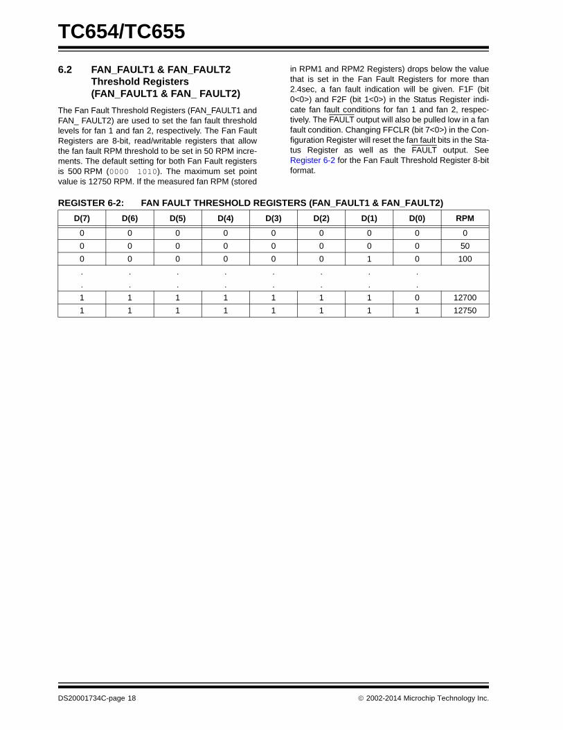
6.2 FAN_FAULT1 & FAN_FAULT2 Threshold Registers (FAN_FAULT1 & FAN_ FAULT2)
The Fan Fault Threshold Registers (FAN_FAULT1 andFAN_ FAULT2) are used to set the fan fault thresholdlevels for fan 1 and fan 2, respectively. The Fan FaultRegisters are 8-bit, read/writable registers that allowthe fan fault RPM threshold to be set in 50 RPM incre-ments. The default setting for both Fan Fault registersis 500 RPM (0000 1010). The maximum set pointvalue is 12750 RPM. If the measured fan RPM (stored
in RPM1 and RPM2 Registers) drops below the valuethat is set in the Fan Fault Registers for more than2.4sec, a fan fault indication will be given. F1F (bit0<0>) and F2F (bit 1<0>) in the Status Register indi-cate fan fault conditions for fan 1 and fan 2, respec-tively. The FAULT output will also be pulled low in a fanfault condition. Changing FFCLR (bit 7<0>) in the Con-figuration Register will reset the fan fault bits in the Sta-tus Register as well as the FAULT output. SeeRegister 6-2 for the Fan Fault Threshold Register 8-bitformat.
REGISTER 6-2: FAN FAULT THRESHOLD REGISTERS (FAN_FAULT1 & FAN_FAULT2)
D(7) D(6) D(5) D(4) D(3) D(2) D(1) D(0) RPM
0 0 0 0 0 0 0 0 0
0 0 0 0 0 0 0 0 50
0 0 0 0 0 0 1 0 100
. . . . . . . .
. . . . . . . .
1 1 1 1 1 1 1 0 12700
1 1 1 1 1 1 1 1 12750
DS20001734C-page 18 2002-2014 Microchip Technology Inc.
TC654/TC655
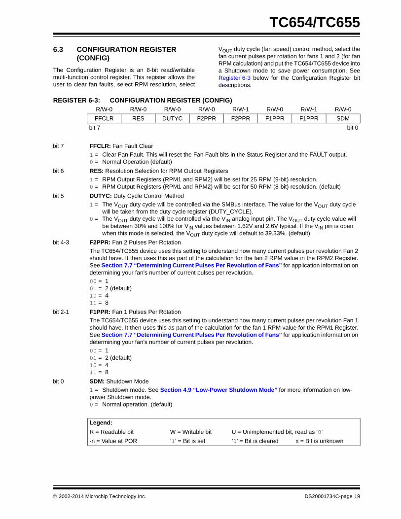
6.3 CONFIGURATION REGISTER (CONFIG)
The Configuration Register is an 8-bit read/writablemulti-function control register. This register allows theuser to clear fan faults, select RPM resolution, select
VOUT duty cycle (fan speed) control method, select thefan current pulses per rotation for fans 1 and 2 (for fanRPM calculation) and put the TC654/TC655 device intoa Shutdown mode to save power consumption. SeeRegister 6-3 below for the Configuration Register bitdescriptions.
REGISTER 6-3: CONFIGURATION REGISTER (CONFIG)R/W-0 R/W-0 R/W-0 R/W-0 R/W-1 R/W-0 R/W-1 R/W-0
FFCLR RES DUTYC F2PPR F2PPR F1PPR F1PPR SDM
bit 7 bit 0
bit 7 FFCLR: Fan Fault Clear
1 = Clear Fan Fault. This will reset the Fan Fault bits in the Status Register and the FAULT output.0 = Normal Operation (default)
bit 6 RES: Resolution Selection for RPM Output Registers
1 = RPM Output Registers (RPM1 and RPM2) will be set for 25 RPM (9-bit) resolution.0 = RPM Output Registers (RPM1 and RPM2) will be set for 50 RPM (8-bit) resolution. (default)
bit 5 DUTYC: Duty Cycle Control Method
1 = The VOUT duty cycle will be controlled via the SMBus interface. The value for the VOUT duty cycle will be taken from the duty cycle register (DUTY_CYCLE).
0 = The VOUT duty cycle will be controlled via the VIN analog input pin. The VOUT duty cycle value will be between 30% and 100% for VIN values between 1.62V and 2.6V typical. If the VIN pin is open when this mode is selected, the VOUT duty cycle will default to 39.33%. (default)
bit 4-3 F2PPR: Fan 2 Pulses Per Rotation
The TC654/TC655 device uses this setting to understand how many current pulses per revolution Fan 2should have. It then uses this as part of the calculation for the fan 2 RPM value in the RPM2 Register.See Section 7.7 “Determining Current Pulses Per Revolution of Fans” for application information ondetermining your fan’s number of current pulses per revolution.
00 = 101 = 2 (default)10 = 411 = 8
bit 2-1 F1PPR: Fan 1 Pulses Per Rotation
The TC654/TC655 device uses this setting to understand how many current pulses per revolution Fan 1should have. It then uses this as part of the calculation for the fan 1 RPM value for the RPM1 Register.See Section 7.7 “Determining Current Pulses Per Revolution of Fans” for application information ondetermining your fan’s number of current pulses per revolution.
00 = 101 = 2 (default)10 = 411 = 8
bit 0 SDM: Shutdown Mode
1 = Shutdown mode. See Section 4.9 “Low-Power Shutdown Mode” for more information on low-power Shutdown mode.0 = Normal operation. (default)
Legend:
R = Readable bit W = Writable bit U = Unimplemented bit, read as ‘0’
-n = Value at POR ’1’ = Bit is set ’0’ = Bit is cleared x = Bit is unknown
2002-2014 Microchip Technology Inc. DS20001734C-page 19
TC654/TC655
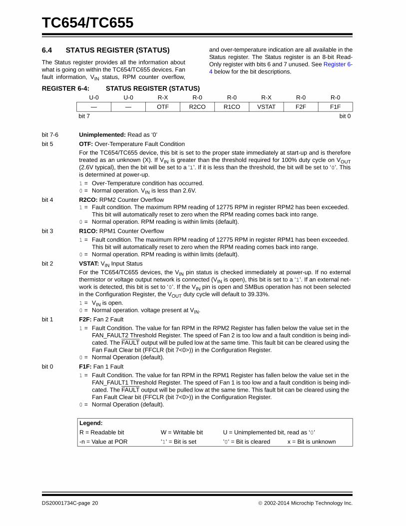
6.4 STATUS REGISTER (STATUS)
The Status register provides all the information aboutwhat is going on within the TC654/TC655 devices. Fanfault information, VIN status, RPM counter overflow,
and over-temperature indication are all available in theStatus register. The Status register is an 8-bit Read-Only register with bits 6 and 7 unused. See Register 6-4 below for the bit descriptions.
REGISTER 6-4: STATUS REGISTER (STATUS)U-0 U-0 R-X R-0 R-0 R-X R-0 R-0
— — OTF R2CO R1CO VSTAT F2F F1F
bit 7 bit 0
bit 7-6 Unimplemented: Read as ‘0’
bit 5 OTF: Over-Temperature Fault Condition
For the TC654/TC655 device, this bit is set to the proper state immediately at start-up and is thereforetreated as an unknown (X). If VIN is greater than the threshold required for 100% duty cycle on VOUT(2.6V typical), then the bit will be set to a ‘1’. If it is less than the threshold, the bit will be set to ‘0’. Thisis determined at power-up.
1 = Over-Temperature condition has occurred.0 = Normal operation. VIN is less than 2.6V.
bit 4 R2CO: RPM2 Counter Overflow1 = Fault condition. The maximum RPM reading of 12775 RPM in register RPM2 has been exceeded.
This bit will automatically reset to zero when the RPM reading comes back into range.0 = Normal operation. RPM reading is within limits (default).
bit 3 R1CO: RPM1 Counter Overflow
1 = Fault condition. The maximum RPM reading of 12775 RPM in register RPM1 has been exceeded. This bit will automatically reset to zero when the RPM reading comes back into range.
0 = Normal operation. RPM reading is within limits (default).
bit 2 VSTAT: VIN Input Status
For the TC654/TC655 devices, the VIN pin status is checked immediately at power-up. If no externalthermistor or voltage output network is connected (VIN is open), this bit is set to a ‘1’. If an external net-work is detected, this bit is set to ‘0’. If the VIN pin is open and SMBus operation has not been selectedin the Configuration Register, the VOUT duty cycle will default to 39.33%.
1 = VIN is open.0 = Normal operation. voltage present at VIN.
bit 1 F2F: Fan 2 Fault
1 = Fault Condition. The value for fan RPM in the RPM2 Register has fallen below the value set in the FAN_FAULT2 Threshold Register. The speed of Fan 2 is too low and a fault condition is being indi-cated. The FAULT output will be pulled low at the same time. This fault bit can be cleared using the Fan Fault Clear bit (FFCLR (bit 7<0>)) in the Configuration Register.
0 = Normal Operation (default).
bit 0 F1F: Fan 1 Fault
1 = Fault Condition. The value for fan RPM in the RPM1 Register has fallen below the value set in the FAN_FAULT1 Threshold Register. The speed of Fan 1 is too low and a fault condition is being indi-cated. The FAULT output will be pulled low at the same time. This fault bit can be cleared using the Fan Fault Clear bit (FFCLR (bit 7<0>)) in the Configuration Register.
0 = Normal Operation (default).
Legend:
R = Readable bit W = Writable bit U = Unimplemented bit, read as ‘0’
-n = Value at POR ’1’ = Bit is set ’0’ = Bit is cleared x = Bit is unknown
DS20001734C-page 20 2002-2014 Microchip Technology Inc.
TC654/TC655
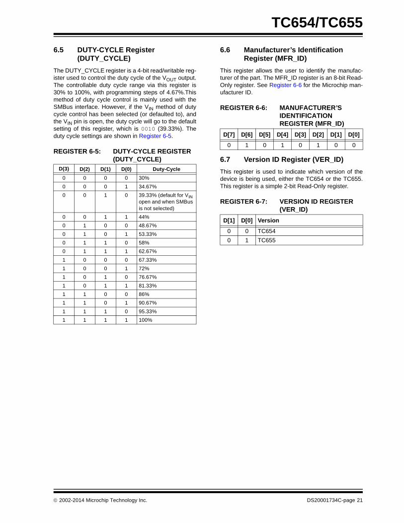
6.5 DUTY-CYCLE Register (DUTY_CYCLE)
The DUTY_CYCLE register is a 4-bit read/writable reg-ister used to control the duty cycle of the VOUT output.The controllable duty cycle range via this register is30% to 100%, with programming steps of 4.67%.Thismethod of duty cycle control is mainly used with theSMBus interface. However, if the VIN method of dutycycle control has been selected (or defaulted to), andthe VIN pin is open, the duty cycle will go to the defaultsetting of this register, which is 0010 (39.33%). Theduty cycle settings are shown in Register 6-5.
REGISTER 6-5: DUTY-CYCLE REGISTER (DUTY_CYCLE)
6.6 Manufacturer’s Identification Register (MFR_ID)
This register allows the user to identify the manufac-turer of the part. The MFR_ID register is an 8-bit Read-Only register. See Register 6-6 for the Microchip man-ufacturer ID.
REGISTER 6-6: MANUFACTURER’S IDENTIFICATION REGISTER (MFR_ID)
6.7 Version ID Register (VER_ID)
This register is used to indicate which version of thedevice is being used, either the TC654 or the TC655.This register is a simple 2-bit Read-Only register.
REGISTER 6-7: VERSION ID REGISTER (VER_ID)
D(3) D(2) D(1) D(0) Duty-Cycle
0 0 0 0 30%
0 0 0 1 34.67%
0 0 1 0 39.33% (default for VIN open and when SMBus is not selected)
0 0 1 1 44%
0 1 0 0 48.67%
0 1 0 1 53.33%
0 1 1 0 58%
0 1 1 1 62.67%
1 0 0 0 67.33%
1 0 0 1 72%
1 0 1 0 76.67%
1 0 1 1 81.33%
1 1 0 0 86%
1 1 0 1 90.67%
1 1 1 0 95.33%
1 1 1 1 100%
D[7] D[6] D[5] D[4] D[3] D[2] D[1] D[0]
0 1 0 1 0 1 0 0
D[1] D[0] Version
0 0 TC654
0 1 TC655
2002-2014 Microchip Technology Inc. DS20001734C-page 21
TC654/TC655
7.0 APPLICATIONS INFORMATION
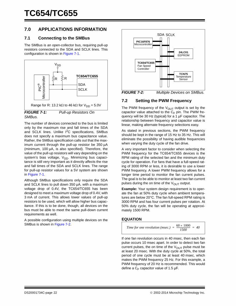
7.1 Connecting to the SMBus
The SMBus is an open-collector bus, requiring pull-upresistors connected to the SDA and SCLK lines. Thisconfiguration is shown in Figure 7-1.
FIGURE 7-1: Pull-up Resistors On SMBus.
The number of devices connected to the bus is limitedonly by the maximum rise and fall times of the SDAand SCLK lines. Unlike I2C specifications, SMBusdoes not specify a maximum bus capacitance value.Rather, the SMBus specification calls out that the max-imum current through the pull-up resistor be 350 µA(minimum, 100 µA, is also specified). Therefore, thevalue of the pull-up resistors will vary depending on thesystem’s bias voltage, VDD. Minimizing bus capaci-tance is still very important as it directly affects the riseand fall times of the SDA and SCLK lines. The rangefor pull-up resistor values for a 5V system are shownin Figure 7-1.
Although SMBus specifications only require the SDAand SCLK lines to pull down 350 µA, with a maximumvoltage drop of 0.4V, the TC654/TC655 has beendesigned to meet a maximum voltage drop of 0.4V, with3 mA of current. This allows lower values of pull-upresistors to be used, which will allow higher bus capac-itance. If this is to be done, though, all devices on thebus must be able to meet the same pull-down currentrequirements as well.
A possible configuration using multiple devices on theSMBus is shown in Figure 7-2.
FIGURE 7-2: Multiple Devices on SMBus.
7.2 Setting the PWM Frequency
The PWM frequency of the VOUT output is set by thecapacitor value attached to the CF pin. The PWM fre-quency will be 30 Hz (typical) for a 1 µF capacitor. Therelationship between frequency and capacitor value islinear, making alternate frequency selections easy.
As stated in previous sections, the PWM frequencyshould be kept in the range of 15 Hz to 35 Hz. This willeliminate the possibility of having audible frequencieswhen varying the duty cycle of the fan drive.
A very important factor to consider when selecting thePWM frequency for the TC654/TC655 devices is theRPM rating of the selected fan and the minimum dutycycle for operation. For fans that have a full-speed rat-ing of 3000 RPM or less, it is desirable to use a lowerPWM frequency. A lower PWM frequency allows for alonger time period to monitor the fan current pulses.The goal is to be able to monitor at least two fan currentpulses during the on time of the VOUT output.
Example: Your system design requirement is to oper-ate the fan at 50% duty cycle when ambient tempera-tures are below 20°C. The fan full-speed RPM rating is3000 RPM and has four current pulses per rotation. At50% duty cycle, the fan will be operating at approxi-mately 1500 RPM.
EQUATION
If one fan revolution occurs in 40 msec, then each fanpulse occurs 10 msec apart. In order to detect two fancurrent pulses, the on time of the VOUT pulse must beat least 20 msec. With the duty cycle at 50%, the totalperiod of one cycle must be at least 40 msec, whichmakes the PWM frequency 25 Hz. For this example, aPWM frequency of 20 Hz is recommended. This woulddefine a CF capacitor value of 1.5 µF.
PIC
® SDA
SCLK
VDD
RR
Mic
roco
ntr
olle
r TC654/TC655
Range for R: 13.2 kto 46 k for VDD = 5.0V
SDA SCLK
PIC16F876Microcontroller
TCN75Temperature
Sensor
24LC01EEPROM
TC654/TC655Fan SpeedController
Time for one revolution (msec.)60 1000
1500------------------------ 40= =
DS20001734C-page 22 2002-2014 Microchip Technology Inc.
TC654/TC655
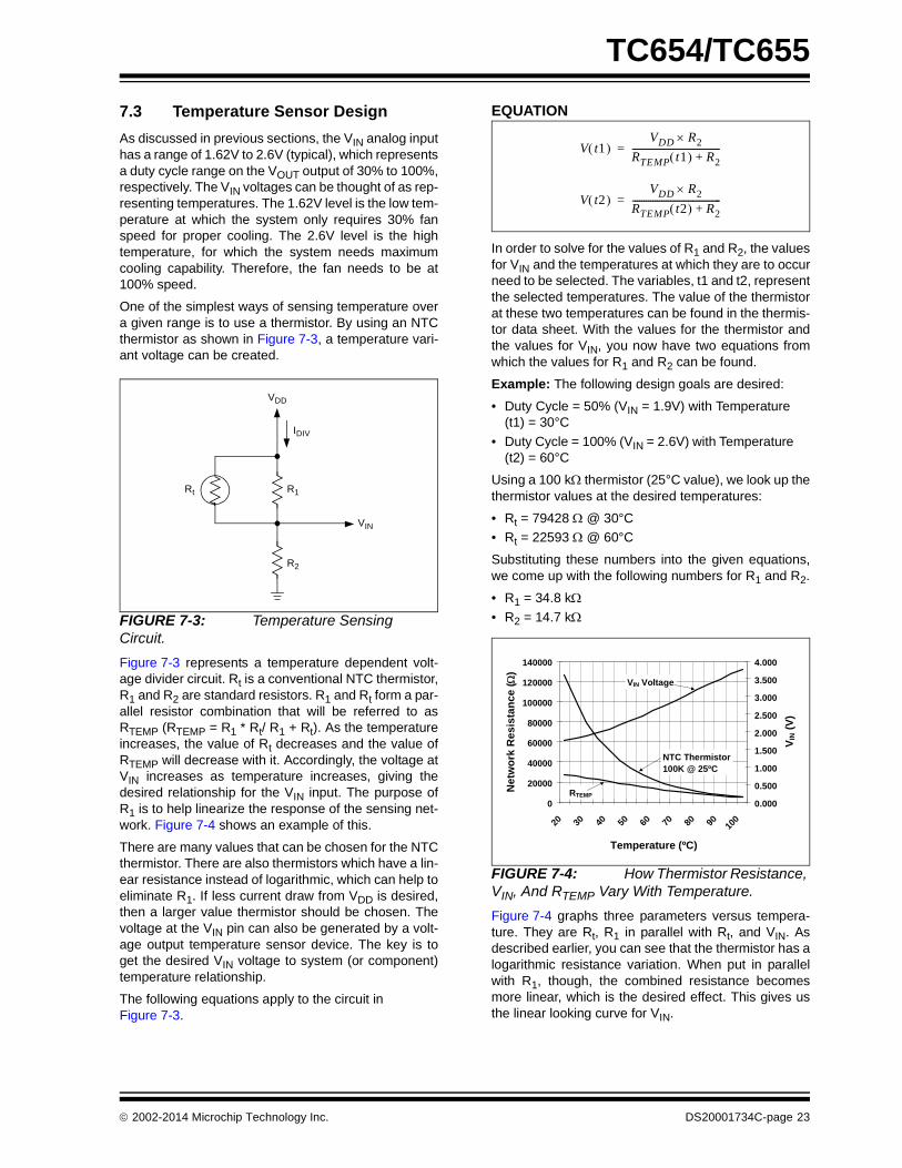
7.3 Temperature Sensor Design
As discussed in previous sections, the VIN analog inputhas a range of 1.62V to 2.6V (typical), which representsa duty cycle range on the VOUT output of 30% to 100%,respectively. The VIN voltages can be thought of as rep-resenting temperatures. The 1.62V level is the low tem-perature at which the system only requires 30% fanspeed for proper cooling. The 2.6V level is the hightemperature, for which the system needs maximumcooling capability. Therefore, the fan needs to be at100% speed.
One of the simplest ways of sensing temperature overa given range is to use a thermistor. By using an NTCthermistor as shown in Figure 7-3, a temperature vari-ant voltage can be created.
FIGURE 7-3: Temperature Sensing Circuit.
Figure 7-3 represents a temperature dependent volt-age divider circuit. Rt is a conventional NTC thermistor,R1 and R2 are standard resistors. R1 and Rt form a par-allel resistor combination that will be referred to asRTEMP (RTEMP = R1 * Rt/ R1 + Rt). As the temperatureincreases, the value of Rt decreases and the value ofRTEMP will decrease with it. Accordingly, the voltage atVIN increases as temperature increases, giving thedesired relationship for the VIN input. The purpose ofR1 is to help linearize the response of the sensing net-work. Figure 7-4 shows an example of this.
There are many values that can be chosen for the NTCthermistor. There are also thermistors which have a lin-ear resistance instead of logarithmic, which can help toeliminate R1. If less current draw from VDD is desired,then a larger value thermistor should be chosen. Thevoltage at the VIN pin can also be generated by a volt-age output temperature sensor device. The key is toget the desired VIN voltage to system (or component)temperature relationship.
The following equations apply to the circuit in Figure 7-3.
EQUATION
In order to solve for the values of R1 and R2, the valuesfor VIN and the temperatures at which they are to occurneed to be selected. The variables, t1 and t2, representthe selected temperatures. The value of the thermistorat these two temperatures can be found in the thermis-tor data sheet. With the values for the thermistor andthe values for VIN, you now have two equations fromwhich the values for R1 and R2 can be found.
Example: The following design goals are desired:
• Duty Cycle = 50% (VIN = 1.9V) with Temperature (t1) = 30°C
• Duty Cycle = 100% (VIN = 2.6V) with Temperature (t2) = 60°C
Using a 100 k thermistor (25°C value), we look up thethermistor values at the desired temperatures:
• Rt = 79428 @ 30°C
• Rt = 22593 @ 60°C
Substituting these numbers into the given equations,we come up with the following numbers for R1 and R2.
• R1 = 34.8 k• R2 = 14.7 k
FIGURE 7-4: How Thermistor Resistance, VIN, And RTEMP Vary With Temperature.
Figure 7-4 graphs three parameters versus tempera-ture. They are Rt, R1 in parallel with Rt, and VIN. Asdescribed earlier, you can see that the thermistor has alogarithmic resistance variation. When put in parallelwith R1, though, the combined resistance becomesmore linear, which is the desired effect. This gives usthe linear looking curve for VIN.
R2
R1Rt
IDIV
VIN
VDD
V t1 VDD R2
RTEMP t1 R2+----------------------------------------=
V t2 VDD R2
RTEMP t2 R2+----------------------------------------=
0
20000
40000
60000
80000
100000
120000
140000
20 30 40 50 60 70 80 90 100
Temperature (ºC)
Ne
two
rk R
es
ista
nc
e (
)
0.000
0.500
1.000
1.500
2.000
2.500
3.000
3.500
4.000
VIN
(V
)
NTC Thermistor100K @ 25ºC
VIN Voltage
RTEMP
2002-2014 Microchip Technology Inc. DS20001734C-page 23
TC654/TC655
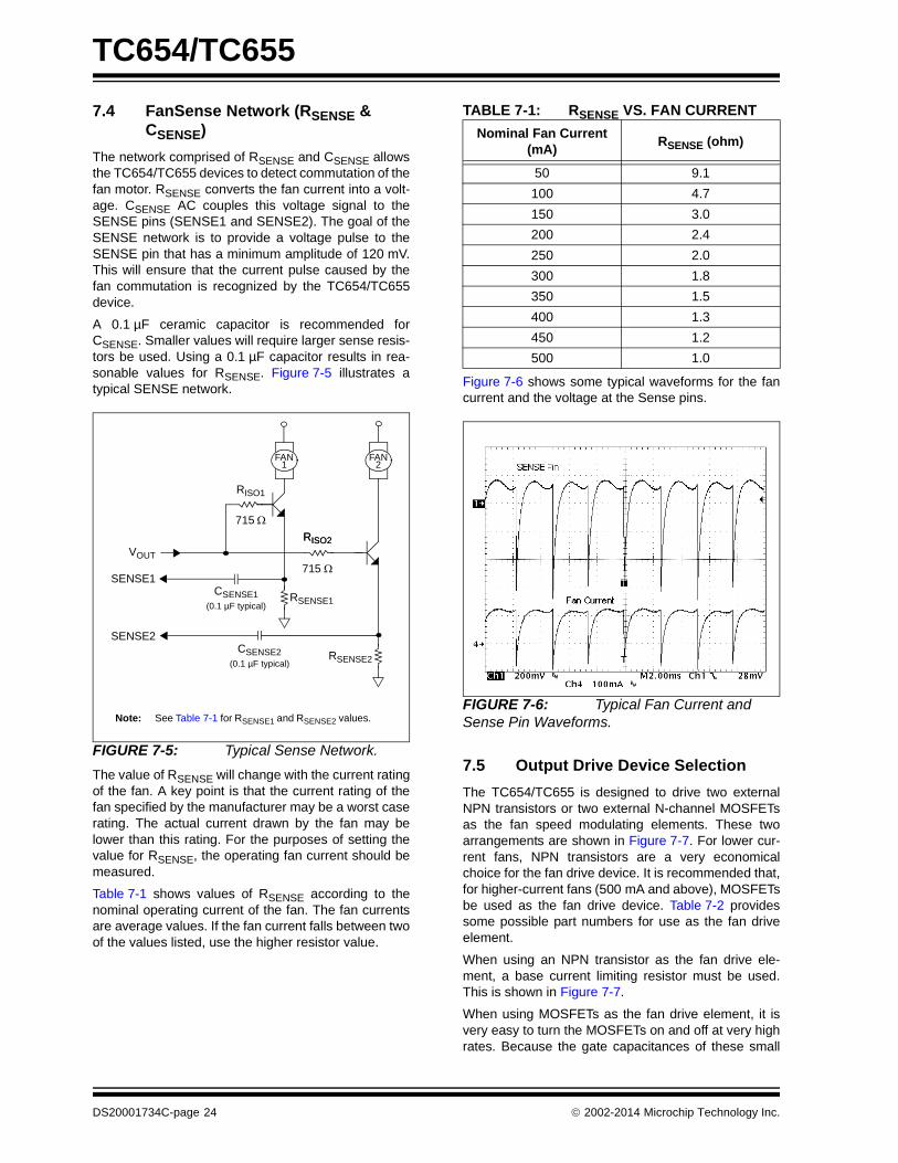
7.4 FanSense Network (RSENSE & CSENSE)
The network comprised of RSENSE and CSENSE allowsthe TC654/TC655 devices to detect commutation of thefan motor. RSENSE converts the fan current into a volt-age. CSENSE AC couples this voltage signal to theSENSE pins (SENSE1 and SENSE2). The goal of theSENSE network is to provide a voltage pulse to theSENSE pin that has a minimum amplitude of 120 mV.This will ensure that the current pulse caused by thefan commutation is recognized by the TC654/TC655device.
A 0.1 µF ceramic capacitor is recommended forCSENSE. Smaller values will require larger sense resis-tors be used. Using a 0.1 µF capacitor results in rea-sonable values for RSENSE. Figure 7-5 illustrates atypical SENSE network.
FIGURE 7-5: Typical Sense Network.
The value of RSENSE will change with the current ratingof the fan. A key point is that the current rating of thefan specified by the manufacturer may be a worst caserating. The actual current drawn by the fan may belower than this rating. For the purposes of setting thevalue for RSENSE, the operating fan current should bemeasured.
Table 7-1 shows values of RSENSE according to thenominal operating current of the fan. The fan currentsare average values. If the fan current falls between twoof the values listed, use the higher resistor value.
TABLE 7-1: RSENSE VS. FAN CURRENT
Figure 7-6 shows some typical waveforms for the fancurrent and the voltage at the Sense pins.
FIGURE 7-6: Typical Fan Current and Sense Pin Waveforms.
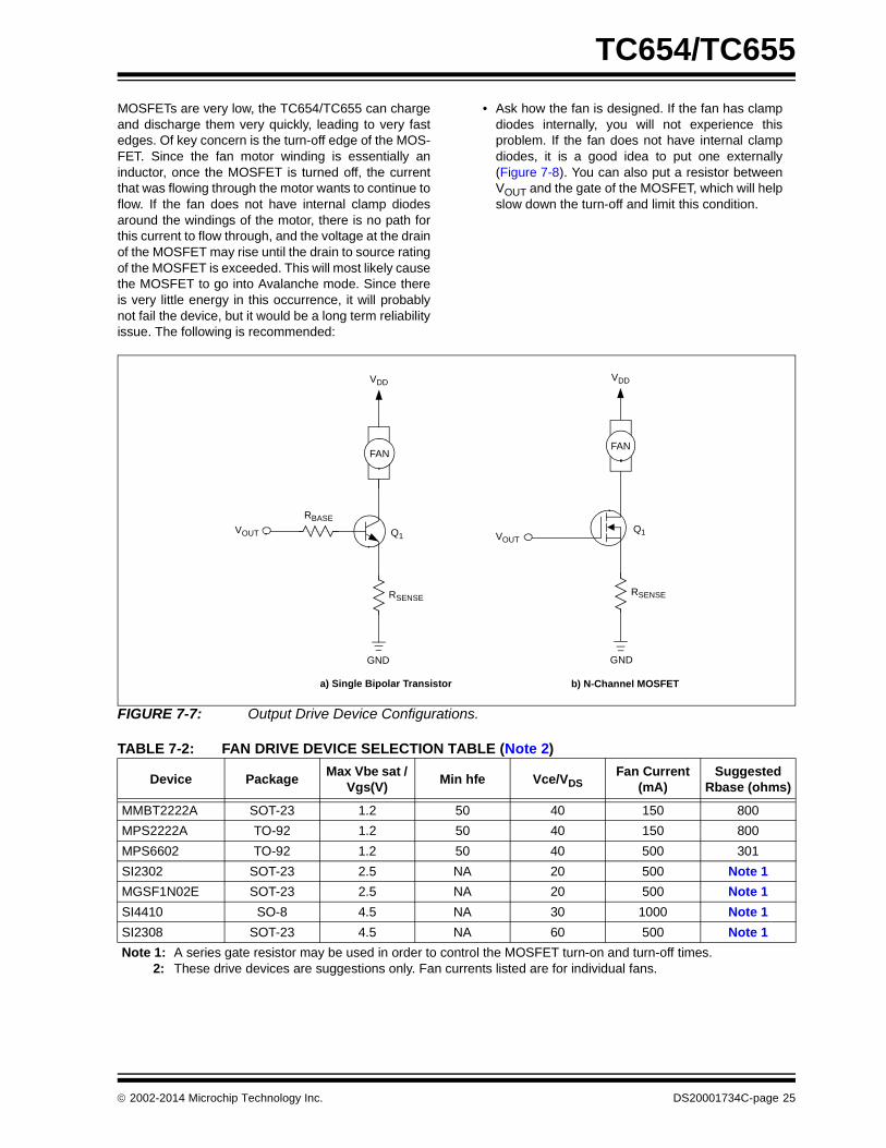
7.5 Output Drive Device Selection
The TC654/TC655 is designed to drive two externalNPN transistors or two external N-channel MOSFETsas the fan speed modulating elements. These twoarrangements are shown in Figure 7-7. For lower cur-rent fans, NPN transistors are a very economicalchoice for the fan drive device. It is recommended that,for higher-current fans (500 mA and above), MOSFETsbe used as the fan drive device. Table 7-2 providessome possible part numbers for use as the fan driveelement.
When using an NPN transistor as the fan drive ele-ment, a base current limiting resistor must be used.This is shown in Figure 7-7.
When using MOSFETs as the fan drive element, it isvery easy to turn the MOSFETs on and off at very highrates. Because the gate capacitances of these small
FAN FAN
RISO1
RISO2
RSENSE2
RSENSE1
CSENSE2
CSENSE1
1 2
SENSE2
SENSE1
VOUT
(0.1 µF typical)
(0.1 µF typical)
715
715
Note: See Table 7-1 for RSENSE1 and RSENSE2 values.
RISO2
Nominal Fan Current (mA)
RSENSE (ohm)
50 9.1
100 4.7
150 3.0
200 2.4
250 2.0
300 1.8
350 1.5
400 1.3
450 1.2
500 1.0
DS20001734C-page 24 2002-2014 Microchip Technology Inc.
TC654/TC655
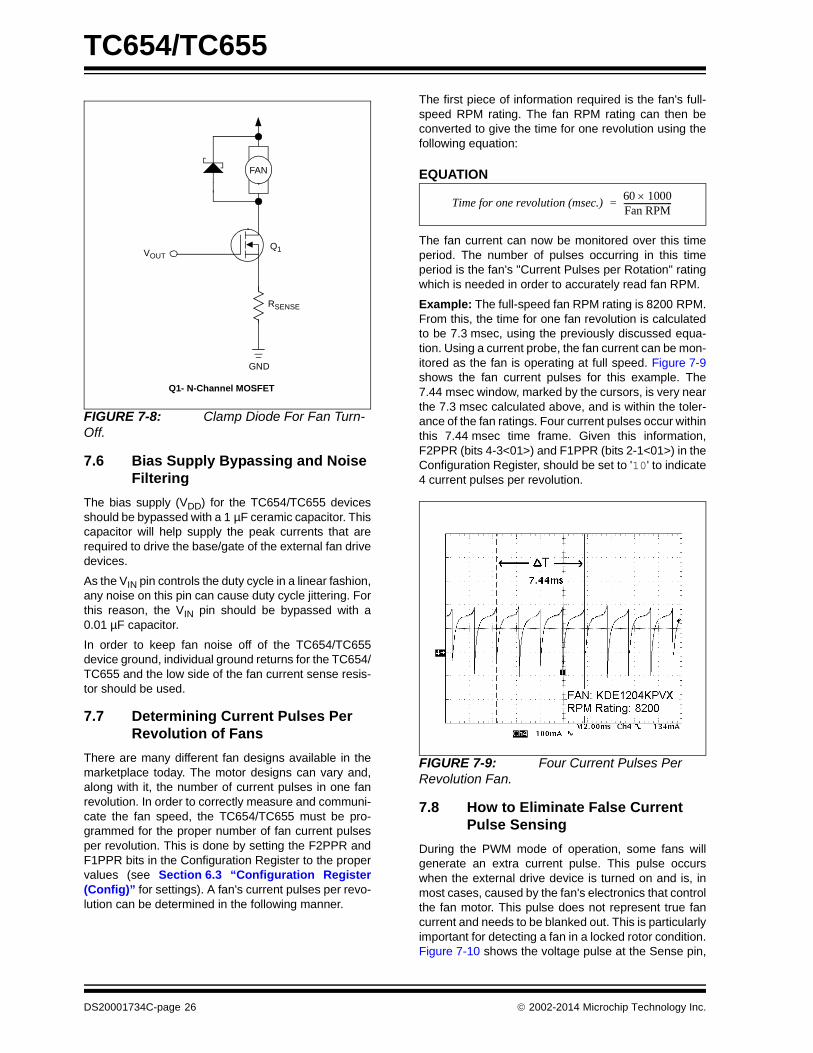
MOSFETs are very low, the TC654/TC655 can chargeand discharge them very quickly, leading to very fastedges. Of key concern is the turn-off edge of the MOS-FET. Since the fan motor winding is essentially aninductor, once the MOSFET is turned off, the currentthat was flowing through the motor wants to continue toflow. If the fan does not have internal clamp diodesaround the windings of the motor, there is no path forthis current to flow through, and the voltage at the drainof the MOSFET may rise until the drain to source ratingof the MOSFET is exceeded. This will most likely causethe MOSFET to go into Avalanche mode. Since thereis very little energy in this occurrence, it will probablynot fail the device, but it would be a long term reliabilityissue. The following is recommended:
• Ask how the fan is designed. If the fan has clampdiodes internally, you will not experience thisproblem. If the fan does not have internal clampdiodes, it is a good idea to put one externally(Figure 7-8). You can also put a resistor betweenVOUT and the gate of the MOSFET, which will helpslow down the turn-off and limit this condition.
FIGURE 7-7: Output Drive Device Configurations.
TABLE 7-2: FAN DRIVE DEVICE SELECTION TABLE (Note 2)
Device PackageMax Vbe sat /
Vgs(V)Min hfe Vce/VDS
Fan Current (mA)
Suggested Rbase (ohms)
MMBT2222A SOT-23 1.2 50 40 150 800
MPS2222A TO-92 1.2 50 40 150 800
MPS6602 TO-92 1.2 50 40 500 301
SI2302 SOT-23 2.5 NA 20 500 Note 1
MGSF1N02E SOT-23 2.5 NA 20 500 Note 1
SI4410 SO-8 4.5 NA 30 1000 Note 1
SI2308 SOT-23 4.5 NA 60 500 Note 1
Note 1: A series gate resistor may be used in order to control the MOSFET turn-on and turn-off times.2: These drive devices are suggestions only. Fan currents listed are for individual fans.
Q1
GND
VDD
RSENSE
RBASE
VOUT
FAN
a) Single Bipolar Transistor
Q1
GND
VDD
RSENSE
VOUT
b) N-Channel MOSFET
FAN
2002-2014 Microchip Technology Inc. DS20001734C-page 25
TC654/TC655
FIGURE 7-8: Clamp Diode For Fan Turn-Off.
7.6 Bias Supply Bypassing and Noise Filtering
The bias supply (VDD) for the TC654/TC655 devicesshould be bypassed with a 1 µF ceramic capacitor. Thiscapacitor will help supply the peak currents that arerequired to drive the base/gate of the external fan drivedevices.
As the VIN pin controls the duty cycle in a linear fashion,any noise on this pin can cause duty cycle jittering. Forthis reason, the VIN pin should be bypassed with a0.01 µF capacitor.
In order to keep fan noise off of the TC654/TC655device ground, individual ground returns for the TC654/TC655 and the low side of the fan current sense resis-tor should be used.
7.7 Determining Current Pulses Per Revolution of Fans
There are many different fan designs available in themarketplace today. The motor designs can vary and,along with it, the number of current pulses in one fanrevolution. In order to correctly measure and communi-cate the fan speed, the TC654/TC655 must be pro-grammed for the proper number of fan current pulsesper revolution. This is done by setting the F2PPR andF1PPR bits in the Configuration Register to the propervalues (see Section 6.3 “Configuration Register(Config)” for settings). A fan's current pulses per revo-lution can be determined in the following manner.
The first piece of information required is the fan's full-speed RPM rating. The fan RPM rating can then beconverted to give the time for one revolution using thefollowing equation:
EQUATION
The fan current can now be monitored over this timeperiod. The number of pulses occurring in this timeperiod is the fan's "Current Pulses per Rotation" ratingwhich is needed in order to accurately read fan RPM.
Example: The full-speed fan RPM rating is 8200 RPM.From this, the time for one fan revolution is calculatedto be 7.3 msec, using the previously discussed equa-tion. Using a current probe, the fan current can be mon-itored as the fan is operating at full speed. Figure 7-9shows the fan current pulses for this example. The7.44 msec window, marked by the cursors, is very nearthe 7.3 msec calculated above, and is within the toler-ance of the fan ratings. Four current pulses occur withinthis 7.44 msec time frame. Given this information,F2PPR (bits 4-3<01>) and F1PPR (bits 2-1<01>) in theConfiguration Register, should be set to '10' to indicate4 current pulses per revolution.
FIGURE 7-9: Four Current Pulses Per Revolution Fan.
7.8 How to Eliminate False Current Pulse Sensing
During the PWM mode of operation, some fans willgenerate an extra current pulse. This pulse occurswhen the external drive device is turned on and is, inmost cases, caused by the fan's electronics that controlthe fan motor. This pulse does not represent true fancurrent and needs to be blanked out. This is particularlyimportant for detecting a fan in a locked rotor condition.Figure 7-10 shows the voltage pulse at the Sense pin,
Q1
GND
RSENSE
VOUT
Q1- N-Channel MOSFET
FAN
Time for one revolution (msec.)60 1000Fan RPM------------------------=
DS20001734C-page 26 2002-2014 Microchip Technology Inc.
TC654/TC655
which is caused by the fan's "extra" current pulseduring PWM output turn-on.
FIGURE 7-10: Extra Pulse at Sense Pin.
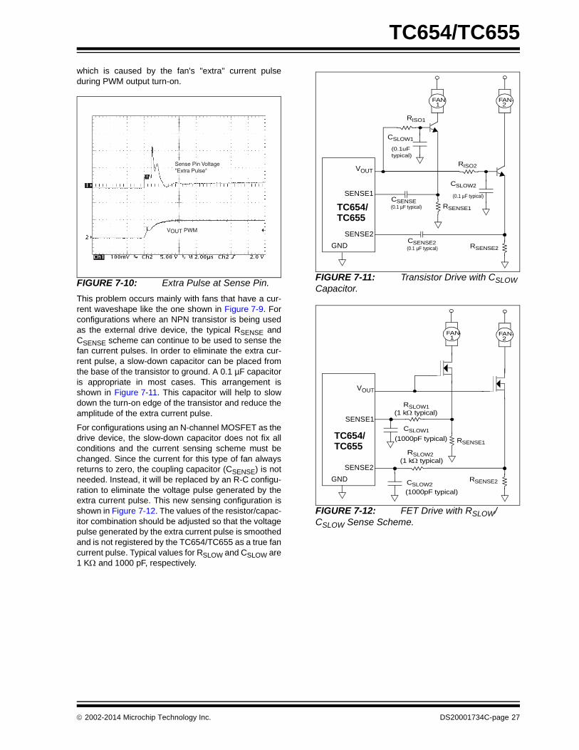
This problem occurs mainly with fans that have a cur-rent waveshape like the one shown in Figure 7-9. Forconfigurations where an NPN transistor is being usedas the external drive device, the typical RSENSE andCSENSE scheme can continue to be used to sense thefan current pulses. In order to eliminate the extra cur-rent pulse, a slow-down capacitor can be placed fromthe base of the transistor to ground. A 0.1 µF capacitoris appropriate in most cases. This arrangement isshown in Figure 7-11. This capacitor will help to slowdown the turn-on edge of the transistor and reduce theamplitude of the extra current pulse.
For configurations using an N-channel MOSFET as thedrive device, the slow-down capacitor does not fix allconditions and the current sensing scheme must bechanged. Since the current for this type of fan alwaysreturns to zero, the coupling capacitor (CSENSE) is notneeded. Instead, it will be replaced by an R-C configu-ration to eliminate the voltage pulse generated by theextra current pulse. This new sensing configuration isshown in Figure 7-12. The values of the resistor/capac-itor combination should be adjusted so that the voltagepulse generated by the extra current pulse is smoothedand is not registered by the TC654/TC655 as a true fancurrent pulse. Typical values for RSLOW and CSLOW are1 K and 1000 pF, respectively.
FIGURE 7-11: Transistor Drive with CSLOW Capacitor.
FIGURE 7-12: FET Drive with RSLOW/CSLOW Sense Scheme.
Sense Pin Voltage"Extra Pulse"
VOUT PWM
FAN FAN
RISO1
RISO2
CSENSE
1 2
(0.1 µF typical)
SENSE2
SENSE1
VOUT
TC654/TC655
(0.1 µF typical)
CSLOW1
(0.1uF
GND
typical)
(0.1 µF typical) RSENSE2CSENSE2
RSENSE1
CSLOW2
FAN FAN
RSLOW2
RSLOW1
RSENSE2
RSENSE1
CSLOW1
1 2
(1000pF typical)
SENSE2
SENSE1
VOUT
TC654/TC655
CSLOW2
(1000pF typical)
GND
(1 k typical)
(1 k typical)
2002-2014 Microchip Technology Inc. DS20001734C-page 27
TC654/TC655
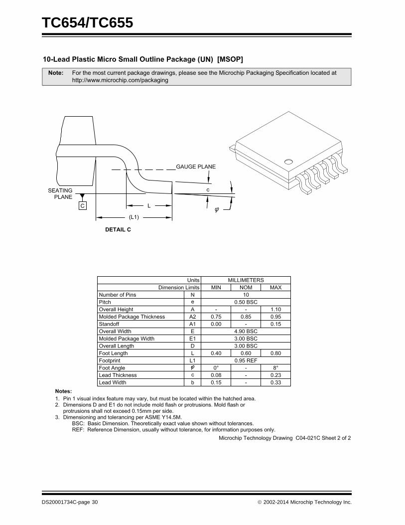
8.0 PACKAGING INFORMATION
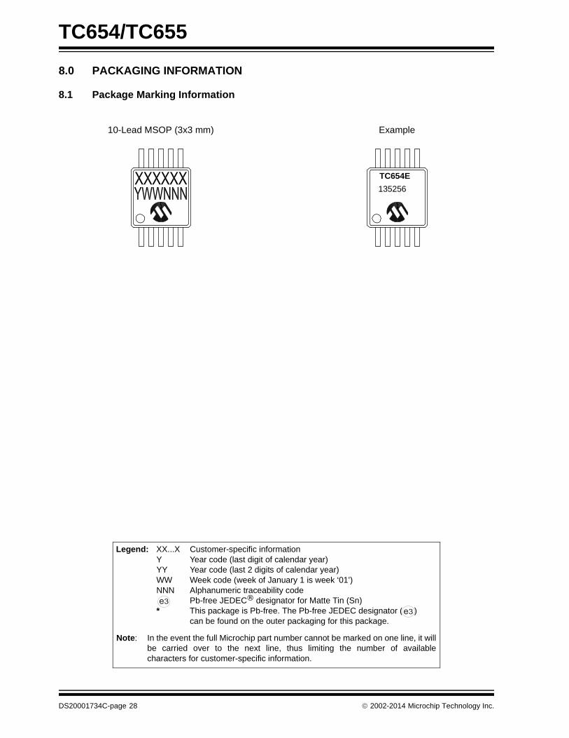
8.1 Package Marking Information
Legend: XX...X Customer-specific informationY Year code (last digit of calendar year)YY Year code (last 2 digits of calendar year)WW Week code (week of January 1 is week ‘01’)NNN Alphanumeric traceability code Pb-free JEDEC® designator for Matte Tin (Sn)* This package is Pb-free. The Pb-free JEDEC designator ( )
can be found on the outer packaging for this package.
Note: In the event the full Microchip part number cannot be marked on one line, it willbe carried over to the next line, thus limiting the number of availablecharacters for customer-specific information.
3e
3e
10-Lead MSOP (3x3 mm) Example
TC654E
135256
DS20001734C-page 28 2002-2014 Microchip Technology Inc.
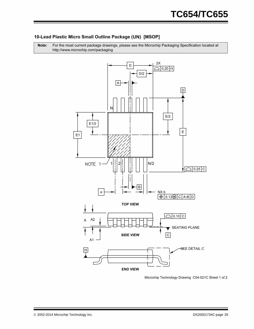
TC654/TC655
Note: For the most current package drawings, please see the Microchip Packaging Specification located at http://www.microchip.com/packaging
UN
2002-2014 Microchip Technology Inc. DS20001734C-page 29
TC654/TC655
Note: For the most current package drawings, please see the Microchip Packaging Specification located at http://www.microchip.com/packaging
UN
DS20001734C-page 30 2002-2014 Microchip Technology Inc.
TC654/TC655
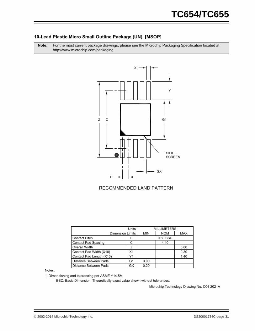
10-Lead Plastic Micro Small Outline Package (UN) [MSOP]
Note: For the most current package drawings, please see the Microchip Packaging Specification located at http://www.microchip.com/packaging
2002-2014 Microchip Technology Inc. DS20001734C-page 31

TC654/TC655
NOTES:
DS20001734C-page 32 2002-2014 Microchip Technology Inc.
TC654/TC655
APPENDIX A: REVISION HISTORY
Revision C (July 2014)
The following is the list of modifications.
1. Updated the package marking drawing.
2. Added Appendix A.
Revision B (January 2013)
The following is the list of modifications.
1. Added a note to the package outline drawing.
Revision A (2002)
• Original Release of this Document.
2002-2014 Microchip Technology Inc. DS20001734C-page 33
TC654/TC655
NOTES:
DS20001734C-page 34 2002-2014 Microchip Technology Inc.
TC654/TC655
PRODUCT IDENTIFICATION SYSTEM
To order or obtain information, e.g., on pricing or delivery, refer to the factory or the listed sales office.
PART NO. X /XX
PackageTemperatureRange
Device
Device: TC654: PWM Fan Speed Controller w/Fault DetectionTC654T: PWM Fan Speed Controller w/Fault Detection
(Tape and Reel)TC655: PWM Fan Speed Controller w/Fault DetectionTC655T: PWM Fan Speed Controller w/Fault Detection
(Tape and Reel)
Temperature Range: E = -40C to +85C
Package: UN = Plastic Micro Small Outline (MSOP), 10-lead
Examples:
a) TC654EUN: PWM Fan Speed Controller w/Fault Detection
b) TC654EUNT: PWM Fan Speed Controllerw/Fault Detection (Tape and Reel)
c) TC655EUN: PWM Fan Speed Controller w/Fault Detection
d) TC655EUNT: PWM Fan Speed Controllerw/Fault Detection (Tape and Reel)
2002-2014 Microchip Technology Inc. DS20001734C-page35
TC654/TC655
NOTES:
DS20001734C-page 36 2002-2014 Microchip Technology Inc.
Note the following details of the code protection feature on Microchip devices:
• Microchip products meet the specification contained in their particular Microchip Data Sheet.
• Microchip believes that its family of products is one of the most secure families of its kind on the market today, when used in the intended manner and under normal conditions.
• There are dishonest and possibly illegal methods used to breach the code protection feature. All of these methods, to our knowledge, require using the Microchip products in a manner outside the operating specifications contained in Microchip’s Data Sheets. Most likely, the person doing so is engaged in theft of intellectual property.
• Microchip is willing to work with the customer who is concerned about the integrity of their code.
• Neither Microchip nor any other semiconductor manufacturer can guarantee the security of their code. Code protection does not mean that we are guaranteeing the product as “unbreakable.”
Code protection is constantly evolving. We at Microchip are committed to continuously improving the code protection features of ourproducts. Attempts to break Microchip’s code protection feature may be a violation of the Digital Millennium Copyright Act. If such actsallow unauthorized access to your software or other copyrighted work, you may have a right to sue for relief under that Act.
Information contained in this publication regarding deviceapplications and the like is provided only for your convenienceand may be superseded by updates. It is your responsibility toensure that your application meets with your specifications.MICROCHIP MAKES NO REPRESENTATIONS ORWARRANTIES OF ANY KIND WHETHER EXPRESS ORIMPLIED, WRITTEN OR ORAL, STATUTORY OROTHERWISE, RELATED TO THE INFORMATION,INCLUDING BUT NOT LIMITED TO ITS CONDITION,QUALITY, PERFORMANCE, MERCHANTABILITY ORFITNESS FOR PURPOSE. Microchip disclaims all liabilityarising from this information and its use. Use of Microchipdevices in life support and/or safety applications is entirely atthe buyer’s risk, and the buyer agrees to defend, indemnify andhold harmless Microchip from any and all damages, claims,suits, or expenses resulting from such use. No licenses areconveyed, implicitly or otherwise, under any Microchipintellectual property rights.
2002-2014 Microchip Technology Inc.
QUALITY MANAGEMENT SYSTEM CERTIFIED BY DNV
== ISO/TS 16949 ==
Trademarks
The Microchip name and logo, the Microchip logo, dsPIC, FlashFlex, flexPWR, JukeBlox, KEELOQ, KEELOQ logo, Kleer, LANCheck, MediaLB, MOST, MOST logo, MPLAB, OptoLyzer, PIC, PICSTART, PIC32 logo, RightTouch, SpyNIC, SST, SST Logo, SuperFlash and UNI/O are registered trademarks of Microchip Technology Incorporated in the U.S.A. and other countries.
The Embedded Control Solutions Company and mTouch are registered trademarks of Microchip Technology Incorporated in the U.S.A.
Analog-for-the-Digital Age, BodyCom, chipKIT, chipKIT logo, CodeGuard, dsPICDEM, dsPICDEM.net, ECAN, In-Circuit Serial Programming, ICSP, Inter-Chip Connectivity, KleerNet, KleerNet logo, MiWi, MPASM, MPF, MPLAB Certified logo, MPLIB, MPLINK, MultiTRAK, NetDetach, Omniscient Code Generation, PICDEM, PICDEM.net, PICkit, PICtail, RightTouch logo, REAL ICE, SQI, Serial Quad I/O, Total Endurance, TSHARC, USBCheck, VariSense, ViewSpan, WiperLock, Wireless DNA, and ZENA are trademarks of Microchip Technology Incorporated in the U.S.A. and other countries.
SQTP is a service mark of Microchip Technology Incorporated in the U.S.A.
Silicon Storage Technology is a registered trademark of Microchip Technology Inc. in other countries.
GestIC is a registered trademarks of Microchip Technology Germany II GmbH & Co. KG, a subsidiary of Microchip Technology Inc., in other countries.
All other trademarks mentioned herein are property of their respective companies.
© 2002-2014, Microchip Technology Incorporated, Printed in the U.S.A., All Rights Reserved.
ISBN: 978-1-63276-362-4
Microchip received ISO/TS-16949:2009 certification for its worldwide
DS20001734C-page 37
headquarters, design and wafer fabrication facilities in Chandler and Tempe, Arizona; Gresham, Oregon and design centers in California and India. The Company’s quality system processes and procedures are for its PIC® MCUs and dsPIC® DSCs, KEELOQ® code hopping devices, Serial EEPROMs, microperipherals, nonvolatile memory and analog products. In addition, Microchip’s quality system for the design and manufacture of development systems is ISO 9001:2000 certified.

DS20001734C-page 38 2002-2014 Microchip Technology Inc.
AMERICASCorporate Office2355 West Chandler Blvd.Chandler, AZ 85224-6199Tel: 480-792-7200 Fax: 480-792-7277Technical Support: http://www.microchip.com/supportWeb Address: www.microchip.com
AtlantaDuluth, GA Tel: 678-957-9614 Fax: 678-957-1455
Austin, TXTel: 512-257-3370
BostonWestborough, MA Tel: 774-760-0087 Fax: 774-760-0088
ChicagoItasca, IL Tel: 630-285-0071 Fax: 630-285-0075
ClevelandIndependence, OH Tel: 216-447-0464 Fax: 216-447-0643
DallasAddison, TX Tel: 972-818-7423 Fax: 972-818-2924
DetroitNovi, MI Tel: 248-848-4000
Houston, TX Tel: 281-894-5983
IndianapolisNoblesville, IN Tel: 317-773-8323Fax: 317-773-5453
Los AngelesMission Viejo, CA Tel: 949-462-9523 Fax: 949-462-9608
New York, NY Tel: 631-435-6000
San Jose, CA Tel: 408-735-9110
Canada - TorontoTel: 905-673-0699 Fax: 905-673-6509
ASIA/PACIFICAsia Pacific OfficeSuites 3707-14, 37th FloorTower 6, The GatewayHarbour City, KowloonHong KongTel: 852-2943-5100Fax: 852-2401-3431
Australia - SydneyTel: 61-2-9868-6733Fax: 61-2-9868-6755
China - BeijingTel: 86-10-8569-7000 Fax: 86-10-8528-2104
China - ChengduTel: 86-28-8665-5511Fax: 86-28-8665-7889
China - ChongqingTel: 86-23-8980-9588Fax: 86-23-8980-9500
China - HangzhouTel: 86-571-8792-8115 Fax: 86-571-8792-8116
China - Hong Kong SARTel: 852-2943-5100 Fax: 852-2401-3431
China - NanjingTel: 86-25-8473-2460Fax: 86-25-8473-2470
China - QingdaoTel: 86-532-8502-7355Fax: 86-532-8502-7205
China - ShanghaiTel: 86-21-5407-5533 Fax: 86-21-5407-5066
China - ShenyangTel: 86-24-2334-2829Fax: 86-24-2334-2393
China - ShenzhenTel: 86-755-8864-2200 Fax: 86-755-8203-1760
China - WuhanTel: 86-27-5980-5300Fax: 86-27-5980-5118
China - XianTel: 86-29-8833-7252Fax: 86-29-8833-7256
China - XiamenTel: 86-592-2388138 Fax: 86-592-2388130
China - ZhuhaiTel: 86-756-3210040 Fax: 86-756-3210049
ASIA/PACIFICIndia - BangaloreTel: 91-80-3090-4444 Fax: 91-80-3090-4123
India - New DelhiTel: 91-11-4160-8631Fax: 91-11-4160-8632
India - PuneTel: 91-20-3019-1500
Japan - OsakaTel: 81-6-6152-7160 Fax: 81-6-6152-9310
Japan - TokyoTel: 81-3-6880- 3770 Fax: 81-3-6880-3771
Korea - DaeguTel: 82-53-744-4301Fax: 82-53-744-4302
Korea - SeoulTel: 82-2-554-7200Fax: 82-2-558-5932 or 82-2-558-5934
Malaysia - Kuala LumpurTel: 60-3-6201-9857Fax: 60-3-6201-9859
Malaysia - PenangTel: 60-4-227-8870Fax: 60-4-227-4068
Philippines - ManilaTel: 63-2-634-9065Fax: 63-2-634-9069
SingaporeTel: 65-6334-8870Fax: 65-6334-8850
Taiwan - Hsin ChuTel: 886-3-5778-366Fax: 886-3-5770-955
Taiwan - KaohsiungTel: 886-7-213-7830
Taiwan - TaipeiTel: 886-2-2508-8600 Fax: 886-2-2508-0102
Thailand - BangkokTel: 66-2-694-1351Fax: 66-2-694-1350
EUROPEAustria - WelsTel: 43-7242-2244-39Fax: 43-7242-2244-393Denmark - CopenhagenTel: 45-4450-2828 Fax: 45-4485-2829
France - ParisTel: 33-1-69-53-63-20 Fax: 33-1-69-30-90-79
Germany - DusseldorfTel: 49-2129-3766400
Germany - MunichTel: 49-89-627-144-0 Fax: 49-89-627-144-44
Germany - PforzheimTel: 49-7231-424750
Italy - Milan Tel: 39-0331-742611 Fax: 39-0331-466781
Italy - VeniceTel: 39-049-7625286
Netherlands - DrunenTel: 31-416-690399 Fax: 31-416-690340
Poland - WarsawTel: 48-22-3325737
Spain - MadridTel: 34-91-708-08-90Fax: 34-91-708-08-91
Sweden - StockholmTel: 46-8-5090-4654
UK - WokinghamTel: 44-118-921-5800Fax: 44-118-921-5820
Worldwide Sales and Service
03/25/14