Embed Size (px)
Citation preview
2015 Microchip Technology Inc. DS20005393B-page 1
MCP39F511
Features• Power Monitoring Accuracy Capable of 0.1%
Error Across 4000:1 Dynamic Range
• Built-In Calculations on Fast 16-Bit Processing Core
- Active, Reactive, Apparent Power
- True RMS Current, RMS Voltage
- Line Frequency, Power Factor
• 64-bit Wide Import and Export Active Energy Accumulation Registers
• 64-bit Four Quadrant Reactive Energy Accumulation Registers
• Signed Active and Reactive Power Outputs
• Dedicated Zero Crossing Detection (ZCD) Pin Output with Less than 200 µs Latency
• Dedicated PWM Output Pin with Programmable Frequency and Duty Cycle
• Automatic Event Pin Control through Fast Voltage Surge Detection Less than 5 ms Delay
• Two Wire Serial Protocol with Selectable Baud Rate Up to 115.2 kbps using Universal Asynchronous Receiver/Transmitter (UART)
• Four Independent Registers for Minimum and Maximum Output Quantity Tracking
• Fast Calibration Routines and Simplified Command Protocol
• 512 Bytes User-Accessible EEPROM through Page Read/Write Commands
• Low-Drift Internal Voltage Reference, 10 ppm/°C Typical
• 28-lead 5x5 QFN Package
• Extended Temperature Range -40°C to +125°C
Applications• Power Monitoring for Home Automation
• Industrial Lighting Power Monitoring
• Real-Time Measurement of Input Power for AC/DC Supplies
• Intelligent Power Distribution Units
DescriptionThe MCP39F511 is a highly integrated, completesingle-phase power-monitoring IC designed forreal-time measurement of input power forAC/DC power supplies, power distribution units,consumer and industrial applications. It includesdual-channel Delta-Sigma ADCs, a 16-bit calculationengine, EEPROM and a flexible 2-wire interface. Anintegrated low-drift voltage reference with 10 ppm/°C inaddition to 94.5 dB of SINAD performance on eachmeasurement channel allows for better than 0.1%accurate designs across a 4000:1 dynamic range.
Package Types
125
2
3
4
5
8 9 10 11 12
21
20
19
18
17
28 27 26 24EVENT1
NC
UART_RX
COMMONA
NC
NC
NC
AV
DD
UA
RT
_T
X
RE
SE
T
DV
DD
DG
ND
MC
LR
EP29
6
7
OSCI
OSCO
13 14
CO
MM
ON
B
PW
M16
15
23 22
RE
FIN
+/O
UT
ZC
DI1+
I1-
V1-
V1+
AN_IN
AGNDD
GN
D
EVENT2
DR
MCP39F5115x5 QFN*
*Includes Exposed Thermal Pad (EP);see Table 3-1.
Power-Monitoring IC with Calculation and Energy Accumulation
MCP39F511
DS20005393B-page 2 2015 Microchip Technology Inc.
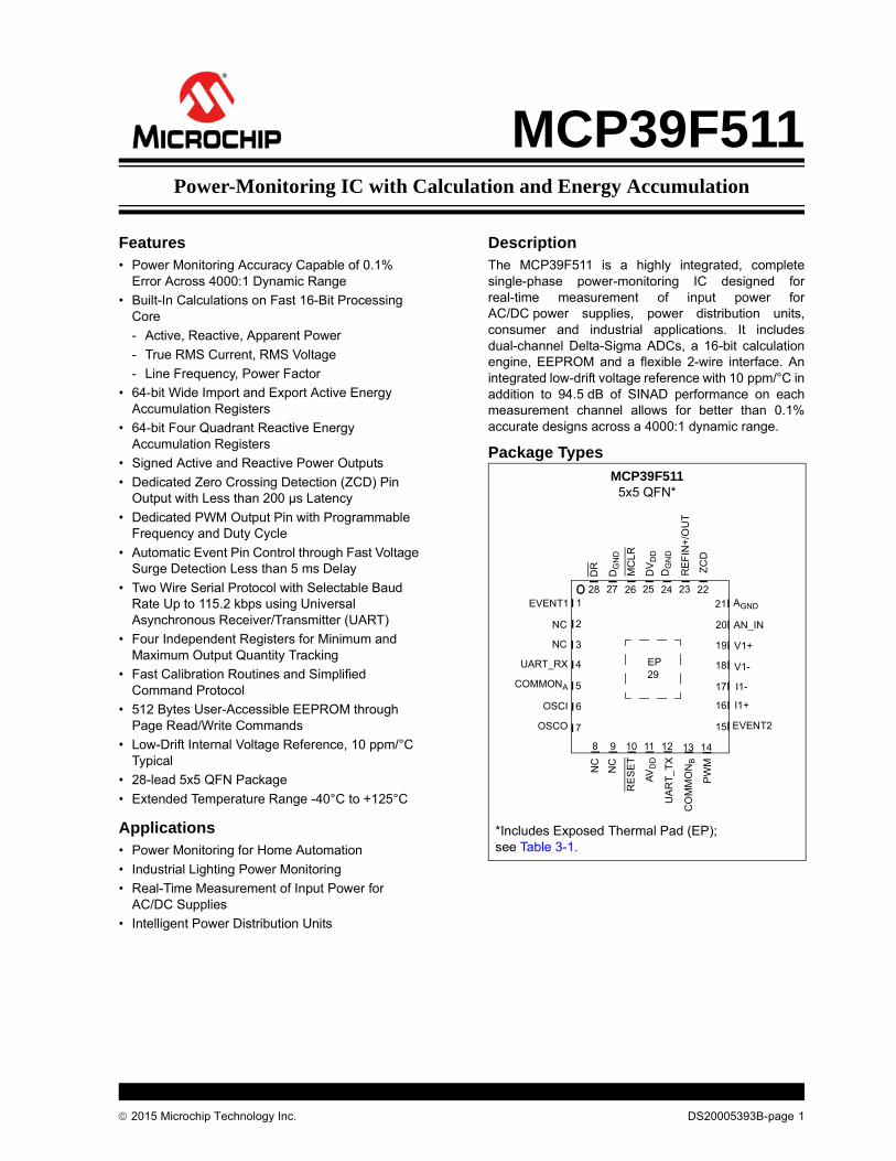
Functional Block Diagram
24-bit Delta-Sigma Multi-level
+- S
INC
3
Dig
ital F
ilte
r
Modulator ADC PGA
I1+
I1-
24-bit Delta-Sigma Multi-level
+- S
INC
3
Dig
ital F
ilte
r
Modulator ADC PGA
V1+
V1-
16-BITCORE
CalculationEngine
(CE)Digital Outputs
UARTSerial
Interface
UART_TX
UART_RX
EVENT1
FLASH
10-bit SARADC
OSCI
OSCO
Timing Generation
InternalOscillator
Generation
AVDD AGND DVDD DGND
EVENT2
PWM
ZCDAN_IN
2015 Microchip Technology Inc. DS20005393B-page 3
MCP39F511
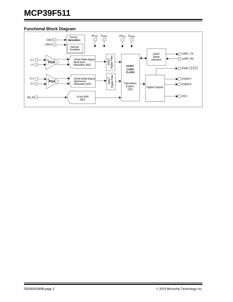
MCP39F511 Typical Application – Single Phase, Two-Wire Application Schematic
DGND
OSCO
OSCI
DVDD RESETAVDD
I1+
I1-
V1-
V1+
NCNCNC
REFIN/OUT+
AGND
COMMONA,B
NC
LOAD
+3.3V
N L
MCP1754
+3.3V
AGNDDGND
+
-
33 nF
33 nF
33 nF
1 k
1 k
1 k
499 k
1 k
4 MHz
22 pF 22 pF
33 nF
0.01 µF
0.47µ F 470
470 µF
10
1 µF0.1 µF
0.1 µF
0.1 µF
AN_IN
2 m
Leave FloatingN.C.
MCP9700A
(OPTIONAL)
+3.3V
to MCU UART
to MCU UARTUART_RX
UART_TX
DR
(OPTIONAL)
Connect on PCB
EVENT1
ZCD
EVENT2
PWM
MCP39F511499 k
Note 1: The MCP39F511 demonstration board uses a switching power supply, however a low-costcapacitive-based supply, as shown here, is sufficient for many applications.
2: The external sensing components shown here, a 2 mΩ shunt, two 499 kΩ and 1 kΩ resistors for the1000:1 voltage divider, are specifically chosen to match the default values for the calibration registersdefined in Section 6.0 “Register Descriptions”. By choosing low-tolerance components of thesevalues (e.g. 1% tolerance), measurement accuracy in the 2-3% range can be achieved with zerocalibration. See Section 9.0 “MCP39F511 Calibration” for more information.
MCP39F511
DS20005393B-page 4 2015 Microchip Technology Inc.
1.0 ELECTRICAL CHARACTERISTICS
Absolute Maximum Ratings †
DVDD .................................................................. -0.3 to +4.5VAVDD .................................................................. -0.3 to +4.0VDigital inputs and outputs w.r.t. AGND............... -0.3V to +4.0VAnalog Inputs (I+,I-,V+,V-) w.r.t. AGND ............... ....-2V to +2VVREF input w.r.t. AGND ........................ ....-0.6V to AVDD +0.6VMaximum Current out of DGND pin..............................300 mAMaximum Current into DVDD pin .................................250 mAMaximum Output Current Sunk by Digital IO ................25 mAMaximum Current Sourced by Digital IO.......................25 mAStorage temperature .....................................-65°C to +150°CAmbient temperature with power applied......-40°C to +125°CSoldering temperature of leads (10 seconds) .............+300°CESD on the analog inputs (HBM,MM) .................4.0 kV, 200VESD on all other pins (HBM,MM) ........................4.0 kV, 200V
† Notice: Stresses above those listed under “MaximumRatings” may cause permanent damage to the device.This is a stress rating only and functional operation ofthe device at those or any other conditions above thoseindicated in the operation listings of this specification isnot implied. Exposure to maximum rating conditions forextended periods may affect device reliability.
1.1 Specifications
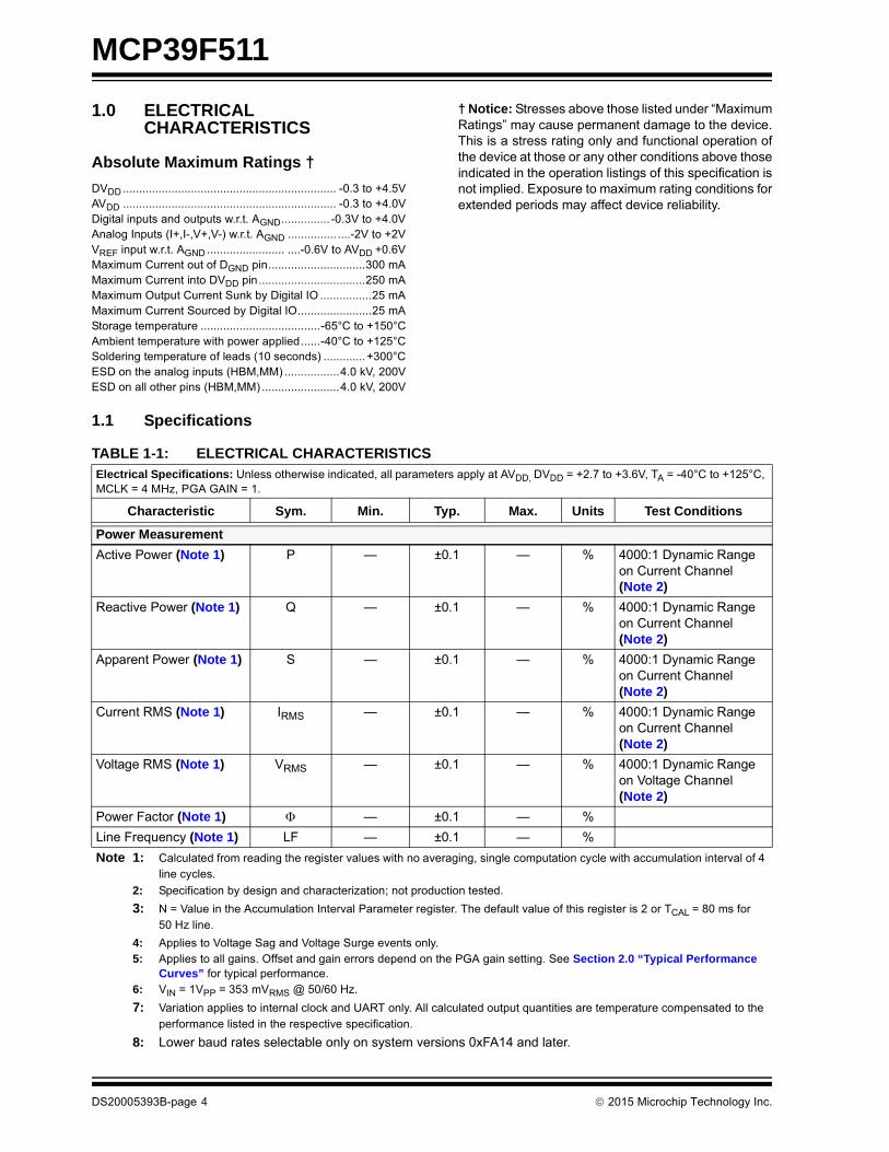
TABLE 1-1: ELECTRICAL CHARACTERISTICSElectrical Specifications: Unless otherwise indicated, all parameters apply at AVDD, DVDD = +2.7 to +3.6V, TA = -40°C to +125°C, MCLK = 4 MHz, PGA GAIN = 1.
Characteristic Sym. Min. Typ. Max. Units Test Conditions
Power Measurement
Active Power (Note 1) P — ±0.1 — % 4000:1 Dynamic Range on Current Channel (Note 2)
Reactive Power (Note 1) Q — ±0.1 — % 4000:1 Dynamic Range on Current Channel (Note 2)
Apparent Power (Note 1) S — ±0.1 — % 4000:1 Dynamic Range on Current Channel (Note 2)
Current RMS (Note 1) IRMS — ±0.1 — % 4000:1 Dynamic Range on Current Channel (Note 2)
Voltage RMS (Note 1) VRMS — ±0.1 — % 4000:1 Dynamic Range on Voltage Channel (Note 2)
Power Factor (Note 1) — ±0.1 — %
Line Frequency (Note 1) LF — ±0.1 — %
Note 1: Calculated from reading the register values with no averaging, single computation cycle with accumulation interval of 4 line cycles.
2: Specification by design and characterization; not production tested.
3: N = Value in the Accumulation Interval Parameter register. The default value of this register is 2 or TCAL = 80 ms for 50 Hz line.
4: Applies to Voltage Sag and Voltage Surge events only.5: Applies to all gains. Offset and gain errors depend on the PGA gain setting. See Section 2.0 “Typical Performance
Curves” for typical performance.6: VIN = 1VPP = 353 mVRMS @ 50/60 Hz.
7: Variation applies to internal clock and UART only. All calculated output quantities are temperature compensated to the performance listed in the respective specification.
8: Lower baud rates selectable only on system versions 0xFA14 and later.
2015 Microchip Technology Inc. DS20005393B-page 5
MCP39F511
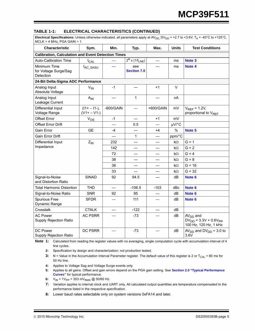
Calibration, Calculation and Event Detection Times
Auto-Calibration Time tCAL — 2N x (1/fLINE) — ms Note 3
Minimum Time for Voltage Surge/Sag Detection
tAC_SASU — see Section 7.0
— ms Note 4
24-Bit Delta-Sigma ADC Performance
Analog Input Absolute Voltage
VIN -1 — +1 V
Analog Input Leakage Current
AIN — 1 — nA
Differential Input Voltage Range
(I1+ – I1-),(V1+ – V1-)
-600/GAIN — +600/GAIN mV VREF = 1.2V, proportional to VREF
Offset Error VOS -1 — +1 mV
Offset Error Drift — 0.5 — µV/°C
Gain Error GE -4 — +4 % Note 5
Gain Error Drift — 1 — ppm/°C
Differential Input Impedance
ZIN 232 — — k G = 1
142 — — k G = 2
72 — — k G = 4
38 — — k G = 8
36 — — k G = 16
33 — — k G = 32
Signal-to-Noise and Distortion Ratio
SINAD 92 94.5 — dB Note 6
Total Harmonic Distortion THD — -106.5 -103 dBc Note 6
Signal-to-Noise Ratio SNR 92 95 — dB Note 6
Spurious Free Dynamic Range
SFDR — 111 — dB Note 6
Crosstalk CTALK — -122 — dB
AC Power Supply Rejection Ratio
AC PSRR — -73 — dB AVDD and DVDD = 3.3V + 0.6VPP, 100 Hz, 120 Hz, 1 kHz
DC Power Supply Rejection Ratio
DC PSRR — -73 — dB AVDD and DVDD = 3.0 to 3.6V
TABLE 1-1: ELECTRICAL CHARACTERISTICS (CONTINUED)Electrical Specifications: Unless otherwise indicated, all parameters apply at AVDD, DVDD = +2.7 to +3.6V, TA = -40°C to +125°C, MCLK = 4 MHz, PGA GAIN = 1.
Characteristic Sym. Min. Typ. Max. Units Test Conditions
Note 1: Calculated from reading the register values with no averaging, single computation cycle with accumulation interval of 4 line cycles.
2: Specification by design and characterization; not production tested.
3: N = Value in the Accumulation Interval Parameter register. The default value of this register is 2 or TCAL = 80 ms for 50 Hz line.
4: Applies to Voltage Sag and Voltage Surge events only.5: Applies to all gains. Offset and gain errors depend on the PGA gain setting. See Section 2.0 “Typical Performance
Curves” for typical performance.6: VIN = 1VPP = 353 mVRMS @ 50/60 Hz.
7: Variation applies to internal clock and UART only. All calculated output quantities are temperature compensated to the performance listed in the respective specification.
8: Lower baud rates selectable only on system versions 0xFA14 and later.
MCP39F511
DS20005393B-page 6 2015 Microchip Technology Inc.
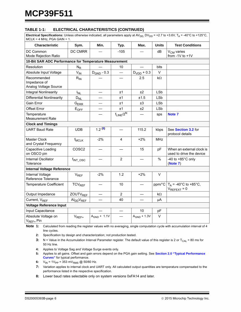
DC Common Mode Rejection Ratio
DC CMRR — -105 — dB VCM varies from -1V to +1V
10-Bit SAR ADC Performance for Temperature Measurement
Resolution NR — 10 — bits
Absolute Input Voltage VIN DGND - 0.3 — DVDD + 0.3 V
Recommended Impedance of Analog Voltage Source
RIN — — 2.5 k
Integral Nonlinearity INL — ±1 ±2 LSb
Differential Nonlinearity DNL — ±1 ±1.5 LSb
Gain Error GERR — ±1 ±3 LSb
Offset Error EOFF — ±1 ±2 LSb
Temperature Measurement Rate
— fLINE/2N — sps Note 7
Clock and Timings
UART Baud Rate UDB 1.2 (8) — 115.2 kbps See Section 3.2 for protocol details
Master Clock and Crystal Frequency
fMCLK -2% 4 +2% MHz
Capacitive Loading on OSCO pin
COSC2 — — 15 pF When an external clock is used to drive the device
Internal Oscillator Tolerance
fINT_OSC — 2 — % -40 to +85°C only (Note 7)
Internal Voltage Reference
Internal Voltage Reference Tolerance
VREF -2% 1.2 +2% V
Temperature Coefficient TCVREF — 10 — ppm/°C TA = -40°C to +85°C, VREFEXT = 0
Output Impedance ZOUTVREF — 2 — k
Current, VREF AIDDVREF — 40 — µA
Voltage Reference Input
Input Capacitance — — 10 pF
Absolute Voltage on VREF+ Pin
VREF+ AGND + 1.1V — AGND + 1.3V V
TABLE 1-1: ELECTRICAL CHARACTERISTICS (CONTINUED)Electrical Specifications: Unless otherwise indicated, all parameters apply at AVDD, DVDD = +2.7 to +3.6V, TA = -40°C to +125°C, MCLK = 4 MHz, PGA GAIN = 1.
Characteristic Sym. Min. Typ. Max. Units Test Conditions
Note 1: Calculated from reading the register values with no averaging, single computation cycle with accumulation interval of 4 line cycles.
2: Specification by design and characterization; not production tested.
3: N = Value in the Accumulation Interval Parameter register. The default value of this register is 2 or TCAL = 80 ms for 50 Hz line.
4: Applies to Voltage Sag and Voltage Surge events only.5: Applies to all gains. Offset and gain errors depend on the PGA gain setting. See Section 2.0 “Typical Performance
Curves” for typical performance.6: VIN = 1VPP = 353 mVRMS @ 50/60 Hz.
7: Variation applies to internal clock and UART only. All calculated output quantities are temperature compensated to the performance listed in the respective specification.
8: Lower baud rates selectable only on system versions 0xFA14 and later.
2015 Microchip Technology Inc. DS20005393B-page 7
MCP39F511
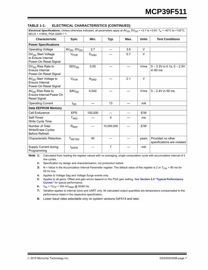
Power Specifications
Operating Voltage AVDD, DVDD 2.7 — 3.6 V
DVDD Start Voltage to Ensure Internal Power-On Reset Signal
VPOR DGND — 0.7 V
DVDD Rise Rate to Ensure Internal Power-On Reset Signal
SDVDD 0.05 — — V/ms 0 – 3.3V in 0.1s, 0 – 2.5V in 60 ms
AVDD Start Voltage to Ensure Internal Power-On Reset Signal
VPOR AGND — 2.1 V
AVDD Rise Rate to Ensure Internal Power On Reset Signal
SAVDD 0.042 — — V/ms 0 – 2.4V in 50 ms
Operating Current IDD — 13 — mA
Data EEPROM Memory
Cell Endurance EPS 100,000 — — E/W
Self-Timed Write Cycle Time
TIWD — 4 — ms
Number of Total Write/Erase Cycles Before Refresh
RREF — 10,000,000 — E/W
Characteristic Retention TRETDD 40 — — years Provided no other specifications are violated
Supply Current during Programming
IDDPD — 7 — mA
TABLE 1-1: ELECTRICAL CHARACTERISTICS (CONTINUED)Electrical Specifications: Unless otherwise indicated, all parameters apply at AVDD, DVDD = +2.7 to +3.6V, TA = -40°C to +125°C, MCLK = 4 MHz, PGA GAIN = 1.
Characteristic Sym. Min. Typ. Max. Units Test Conditions
Note 1: Calculated from reading the register values with no averaging, single computation cycle with accumulation interval of 4 line cycles.
2: Specification by design and characterization; not production tested.
3: N = Value in the Accumulation Interval Parameter register. The default value of this register is 2 or TCAL = 80 ms for 50 Hz line.
4: Applies to Voltage Sag and Voltage Surge events only.5: Applies to all gains. Offset and gain errors depend on the PGA gain setting. See Section 2.0 “Typical Performance
Curves” for typical performance.6: VIN = 1VPP = 353 mVRMS @ 50/60 Hz.
7: Variation applies to internal clock and UART only. All calculated output quantities are temperature compensated to the performance listed in the respective specification.
8: Lower baud rates selectable only on system versions 0xFA14 and later.
MCP39F511
DS20005393B-page 8 2015 Microchip Technology Inc.
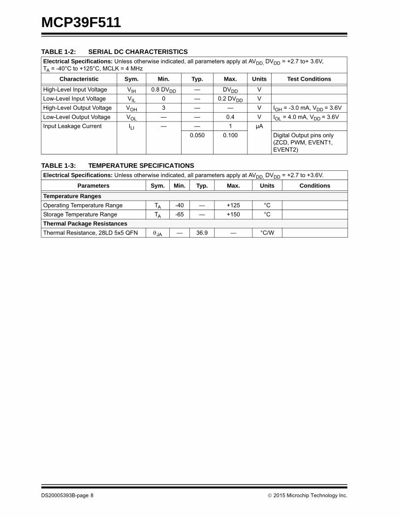
TABLE 1-2: SERIAL DC CHARACTERISTICS
Electrical Specifications: Unless otherwise indicated, all parameters apply at AVDD, DVDD = +2.7 to+ 3.6V, TA = -40°C to +125°C, MCLK = 4 MHz
Characteristic Sym. Min. Typ. Max. Units Test Conditions
High-Level Input Voltage VIH 0.8 DVDD — DVDD V
Low-Level Input Voltage VIL 0 — 0.2 DVDD V
High-Level Output Voltage VOH 3 — — V IOH = -3.0 mA, VDD = 3.6V
Low-Level Output Voltage VOL — — 0.4 V IOL = 4.0 mA, VDD = 3.6V
Input Leakage Current ILI — — 1 µA
0.050 0.100 Digital Output pins only (ZCD, PWM, EVENT1, EVENT2)
TABLE 1-3: TEMPERATURE SPECIFICATIONS
Electrical Specifications: Unless otherwise indicated, all parameters apply at AVDD, DVDD = +2.7 to +3.6V.
Parameters Sym. Min. Typ. Max. Units Conditions
Temperature Ranges
Operating Temperature Range TA -40 — +125 °C
Storage Temperature Range TA -65 — +150 °C
Thermal Package Resistances
Thermal Resistance, 28LD 5x5 QFN JA — 36.9 — °C/W
2015 Microchip Technology Inc. DS20005393B-page 9
MCP39F511
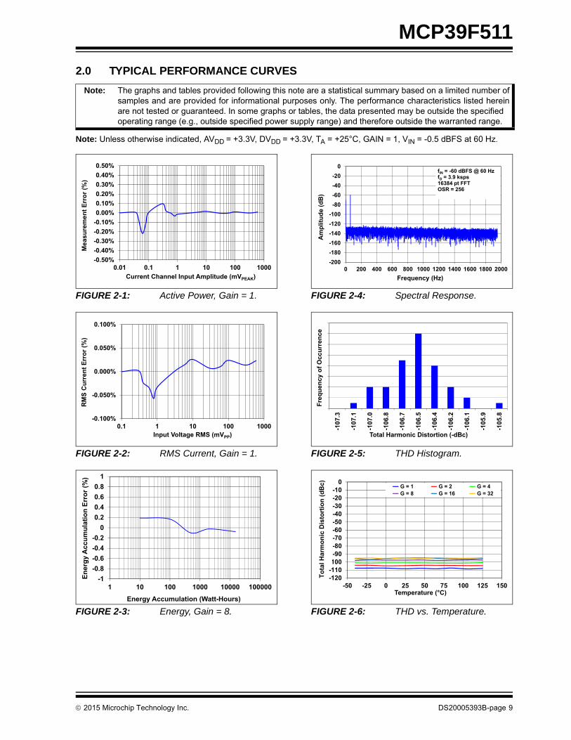
2.0 TYPICAL PERFORMANCE CURVES
Note: Unless otherwise indicated, AVDD = +3.3V, DVDD = +3.3V, TA = +25°C, GAIN = 1, VIN = -0.5 dBFS at 60 Hz.
FIGURE 2-1: Active Power, Gain = 1.
FIGURE 2-2: RMS Current, Gain = 1.
FIGURE 2-3: Energy, Gain = 8.
FIGURE 2-4: Spectral Response.
FIGURE 2-5: THD Histogram.
FIGURE 2-6: THD vs. Temperature.
Note: The graphs and tables provided following this note are a statistical summary based on a limited number ofsamples and are provided for informational purposes only. The performance characteristics listed hereinare not tested or guaranteed. In some graphs or tables, the data presented may be outside the specifiedoperating range (e.g., outside specified power supply range) and therefore outside the warranted range.
-0.50%-0.40%-0.30%-0.20%-0.10%0.00%0.10%0.20%0.30%0.40%0.50%
0.01 0.1 1 10 100 1000
Mea
sure
men
t Err
or (%
)
Current Channel Input Amplitude (mVPEAK)
-0.100%
-0.050%
0.000%
0.050%
0.100%
0.1 1 10 100 1000
RM
S C
urre
nt E
rror
(%)
Input Voltage RMS (mVPP)
-1-0.8-0.6-0.4-0.2
00.20.40.60.8
1
1 10 100 1000 10000 100000
Ener
gy A
ccum
ulat
ion
Erro
r (%
)
Energy Accumulation (Watt-Hours)
-200-180-160-140-120-100
-80-60-40-20
0
0 200 400 600 800 1000 1200 1400 1600 1800 2000
Am
plitu
de (d
B)
Frequency (Hz)
fIN = -60 dBFS @ 60 HzfD = 3.9 ksps16384 pt FFTOSR = 256
-107
.3
-107
.1
-107
.0
-106
.8
-106
.7
-106
.5
-106
.4
-106
.2
-106
.1
-105
.9
-105
.8
Freq
uenc
y of
Occ
urre
nce
Total Harmonic Distortion (-dBc)
-120-110-100
-90-80-70-60-50-40-30-20-10
0
-50 -25 0 25 50 75 100 125 150
Tota
l Hrm
onic
Dis
tort
ion
(dB
c)
Temperature (°C)
G = 1 G = 2 G = 4 G = 8 G = 16 G = 32
MCP39F511
DS20005393B-page 10 2015 Microchip Technology Inc.
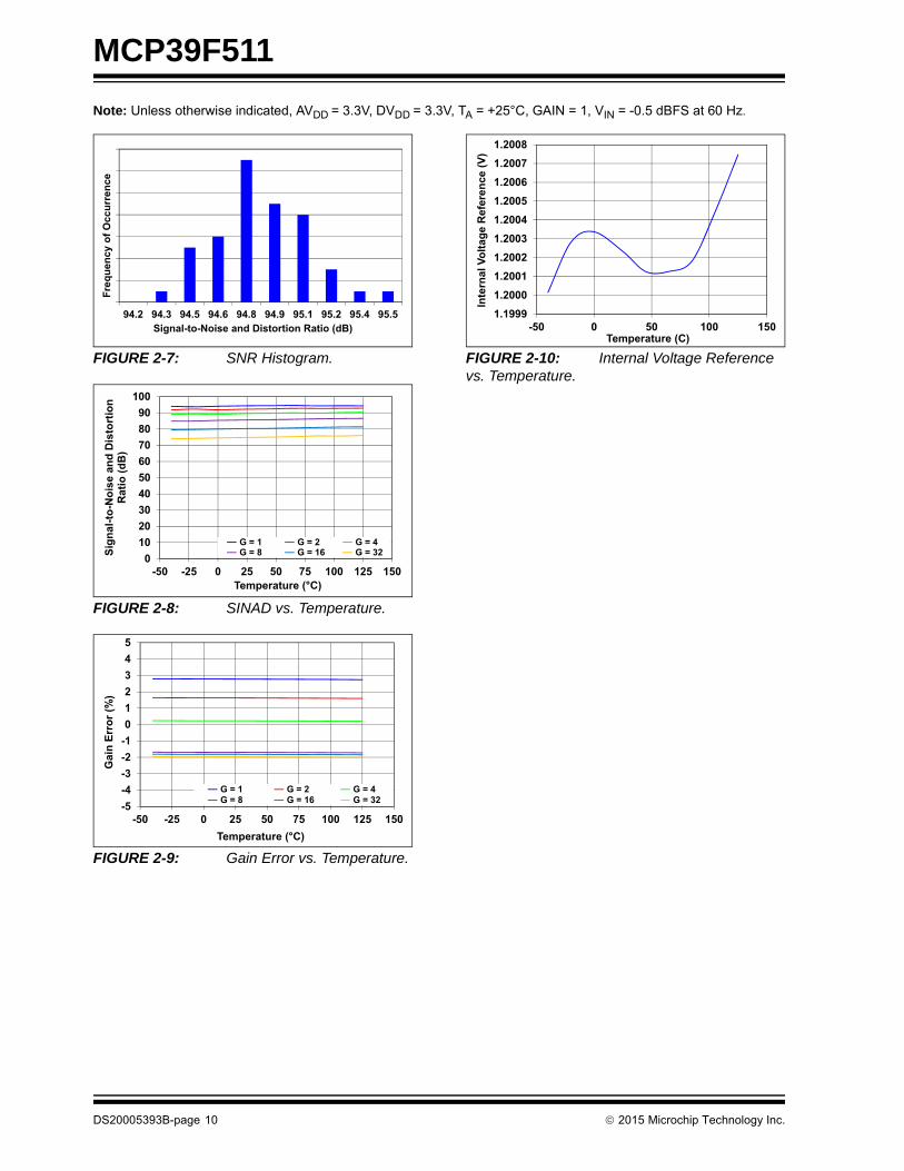
Note: Unless otherwise indicated, AVDD = 3.3V, DVDD = 3.3V, TA = +25°C, GAIN = 1, VIN = -0.5 dBFS at 60 Hz.
FIGURE 2-7: SNR Histogram.
FIGURE 2-8: SINAD vs. Temperature.
FIGURE 2-9: Gain Error vs. Temperature.
FIGURE 2-10: Internal Voltage Reference vs. Temperature.
94.2 94.3 94.5 94.6 94.8 94.9 95.1 95.2 95.4 95.5
Freq
uenc
y of
Occ
urre
nce
Signal-to-Noise and Distortion Ratio (dB)
0102030405060708090
100
-50 -25 0 25 50 75 100 125 150
Sign
al-to
-Noi
se a
nd D
isto
rtio
n R
atio
(dB
)
Temperature (°C)
G = 1 G = 2 G = 4 G = 8 G = 16 G = 32
-5-4-3-2-1012345
-50 -25 0 25 50 75 100 125 150
Gai
n Er
ror (
%)
Temperature (°C)
G = 1 G = 2 G = 4 G = 8 G = 16 G = 32
1.19991.20001.20011.20021.20031.20041.20051.20061.20071.2008
-50 0 50 100 150
Inte
rnal
Vol
tage
Ref
eren
ce (V
)
Temperature (C)
2015 Microchip Technology Inc. DS20005393B-page 11
MCP39F511
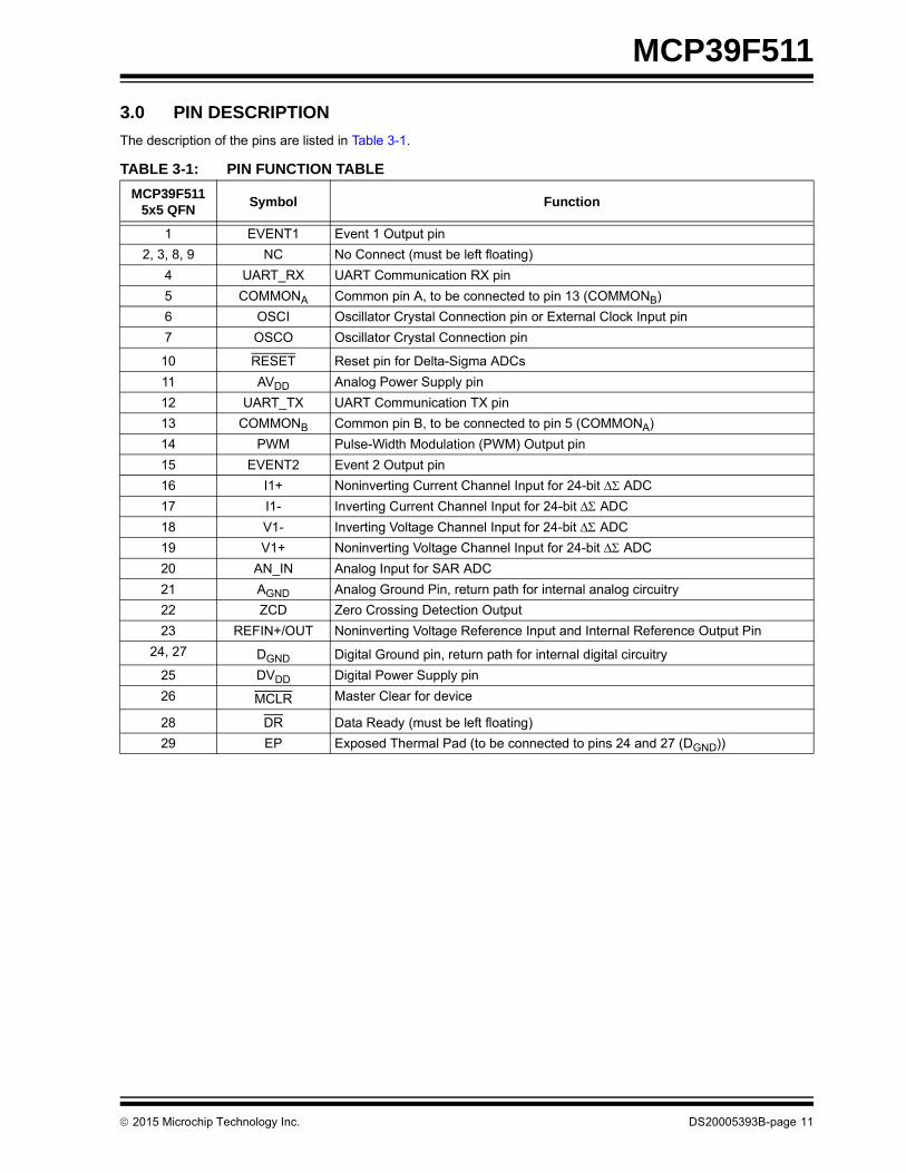
3.0 PIN DESCRIPTION
The description of the pins are listed in Table 3-1.
TABLE 3-1: PIN FUNCTION TABLE
MCP39F5115x5 QFN
Symbol Function
1 EVENT1 Event 1 Output pin
2, 3, 8, 9 NC No Connect (must be left floating)
4 UART_RX UART Communication RX pin
5 COMMONA Common pin A, to be connected to pin 13 (COMMONB)
6 OSCI Oscillator Crystal Connection pin or External Clock Input pin
7 OSCO Oscillator Crystal Connection pin
10 RESET Reset pin for Delta-Sigma ADCs
11 AVDD Analog Power Supply pin
12 UART_TX UART Communication TX pin
13 COMMONB Common pin B, to be connected to pin 5 (COMMONA)
14 PWM Pulse-Width Modulation (PWM) Output pin
15 EVENT2 Event 2 Output pin
16 I1+ Noninverting Current Channel Input for 24-bit ADC
17 I1- Inverting Current Channel Input for 24-bit ADC
18 V1- Inverting Voltage Channel Input for 24-bit ADC
19 V1+ Noninverting Voltage Channel Input for 24-bit ADC
20 AN_IN Analog Input for SAR ADC
21 AGND Analog Ground Pin, return path for internal analog circuitry
22 ZCD Zero Crossing Detection Output
23 REFIN+/OUT Noninverting Voltage Reference Input and Internal Reference Output Pin
24, 27 DGND Digital Ground pin, return path for internal digital circuitry
25 DVDD Digital Power Supply pin
26 MCLR Master Clear for device
28 DR Data Ready (must be left floating)
29 EP Exposed Thermal Pad (to be connected to pins 24 and 27 (DGND))
MCP39F511
DS20005393B-page 12 2015 Microchip Technology Inc.
3.1 Event Output Pins (EVENTn)
These digital output pins can be configured to act asoutput flags based on various internal raise conditions.Control is modified through the Event Configurationregister.
3.2 UART Communication Pins (UART_RX, UART_TX)
The MCP39F511 device contains an asynchronousfull-duplex UART. The UART communication is eightbits with Start and Stop bit. See Section 4.3 “UARTSettings” for more information.
3.3 Common Pins (COMMONA and B)
COMMONA and COMMONB pins are internalconnections for the MCP39F511. These two pinsshould be connected together in the application.
3.4 Oscillator Pins (OSCI/OSCO)
OSCI and OSCO provide the master clock for thedevice. Appropriate load capacitance should beconnected to these pins for proper operation. Anoptional 4 MHz crystal can be connected to these pins.If a crystal of external clock source is not detected, thedevice will clock from the internal 4 MHz oscillator.
3.5 Reset Pin (RESET)
This pin is active-low and places the Delta-SigmaADCs, PGA, internal VREF and other blocks associatedwith the analog front-end in a Reset state when pulledlow. This input is Schmitt-triggered.
3.6 Analog Power Supply Pin (AVDD)
AVDD is the power supply pin for the analog circuitrywithin the MCP39F511.
This pin requires appropriate bypass capacitors andshould be maintained to +2.7V and +3.6V for specifiedoperation. It is recommended to use 0.1 µF ceramiccapacitors.
3.7 Pulse Width Modulator (PWM)
This digital output is a dedicated PWM output that canbe controlled through the PWM Frequency and PWMDuty Cycle registers. See Section 8.0 “Pulse Widthmodulation (PWM)” for more information.
3.8 24-Bit Delta-Sigma ADC Differential Current Channel Input Pins (I1+/I1-)
I1- and I1+ are the two fully-differential current-channelinputs for the Delta-Sigma ADCs.
The linear and specified region of the channels aredependent on the PGA gain. This region correspondsto a differential voltage range of ±600 mVPEAK/GAINwith VREF = 1.2V.
The maximum absolute voltage, with respect to AGND,for each In+/- input pin is ±1V with no distortionand ±6V with no breaking after continuous voltage.
3.9 24-Bit Delta-Sigma ADC Differential Voltage Channel Inputs (V1-/V1+)
V1- and V1+ are the two fully-differentialvoltage-channel inputs for the Delta-Sigma ADCs.
The linear and specified region of the channels aredependent on the PGA gain. This region correspondsto a differential voltage range of ±600 mVPEAK/GAINwith VREF = 1.2V.
The maximum absolute voltage, with respect to AGND,for each VN+/- input pin is ±1V with no distortionand ±2V with no breaking after continuous voltage.
3.10 Analog Input (AN_IN)
This is the input to the analog-to-digital converter thatcan be used for temperature measurement andcompensation. If temperature compensation isrequired in the application, it is advised to connect thelow-power active thermistor IC MCP9700A to this pin.If temperature compensation is not required, this canbe used as a general purpose analog-to-digitalconverter input.
3.11 Analog Ground Pin (AGND)
AGND is the ground connection to internal analogcircuitry (ADCs, PGA, voltage reference, POR). If ananalog ground pin is available on the PCB, it isrecommended that this pin be tied to that plane.
3.12 Zero Crossing Detection (ZCD)
This digital output pin is the output of the zero crossingdetection circuit of the IC. The output here will be alogic output with edges that transition at each zerocrossing of the voltage channel input. For moreinformation see Section 5.13 “Zero CrossingDetection (ZCD)”.
2015 Microchip Technology Inc. DS20005393B-page 13
MCP39F511
3.13 Noninverting Reference Input/Internal Reference Output Pin (REFIN+/OUT)
This pin is the noninverting side of the differentialvoltage reference input for the Delta-Sigma ADCs orthe internal voltage reference output.
For optimal performance, bypass capacitances shouldbe connected between this pin and AGND at all times,even when the internal voltage reference is used.However, these capacitors are not mandatory toensure proper operation.
3.14 Digital Ground Connection Pins (DGND)
DGND is the ground connection to internal digitalcircuitry (SINC filters, oscillator, serial interface). If adigital ground plane is available, it is recommended totie this pin to the digital plane of the PCB. This planeshould also reference all other digital circuitry in thesystem.
3.15 Digital Power Supply Pin (DVDD)
DVDD is the power supply pin for the digital circuitrywithin the MCP39F511. This pin requires appropriatebypass capacitors and should be maintained between+2.7V and +3.6V for specified operation. It isrecommended to use 0.1 µF ceramic capacitors.
3.16 Data-Ready Pin (DR)
The data-ready pin indicates if a new Delta-Sigma A/Dconversion result is ready to be processed. This pin isfor indication only and should be left floating. After eachconversion is finished, a low pulse will take place on thedata-ready pin to indicate the conversion result is readyand an interrupt is generated in the calculation engine(CE). This pulse is synchronous with the line frequencyto ensure an integer number of samples for each linecycle.
3.17 Exposed Thermal Pad (EP)
This pin is the exposed thermal pad. It must beconnected to pin 24 (DGND).
Note: This pin is internally connected to the IRQof the calculation engine and should beleft floating.

MCP39F511
DS20005393B-page 14 2015 Microchip Technology Inc.
NOTES:
2015 Microchip Technology Inc. DS20005393B-page 15
MCP39F511
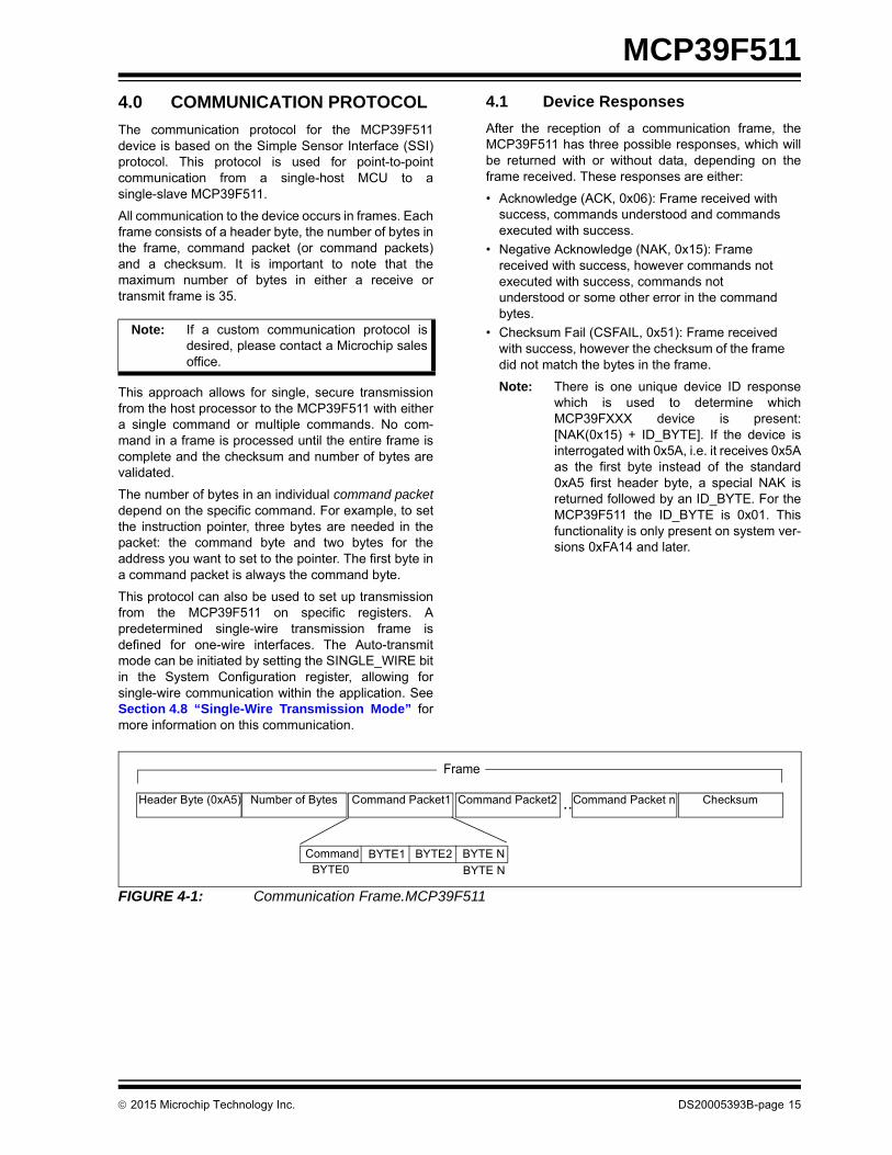
4.0 COMMUNICATION PROTOCOL
The communication protocol for the MCP39F511device is based on the Simple Sensor Interface (SSI)protocol. This protocol is used for point-to-pointcommunication from a single-host MCU to asingle-slave MCP39F511.
All communication to the device occurs in frames. Eachframe consists of a header byte, the number of bytes inthe frame, command packet (or command packets)and a checksum. It is important to note that themaximum number of bytes in either a receive ortransmit frame is 35.
This approach allows for single, secure transmissionfrom the host processor to the MCP39F511 with eithera single command or multiple commands. No com-mand in a frame is processed until the entire frame iscomplete and the checksum and number of bytes arevalidated.
The number of bytes in an individual command packetdepend on the specific command. For example, to setthe instruction pointer, three bytes are needed in thepacket: the command byte and two bytes for theaddress you want to set to the pointer. The first byte ina command packet is always the command byte.
This protocol can also be used to set up transmissionfrom the MCP39F511 on specific registers. Apredetermined single-wire transmission frame isdefined for one-wire interfaces. The Auto-transmitmode can be initiated by setting the SINGLE_WIRE bitin the System Configuration register, allowing forsingle-wire communication within the application. SeeSection 4.8 “Single-Wire Transmission Mode” formore information on this communication.
4.1 Device Responses
After the reception of a communication frame, theMCP39F511 has three possible responses, which willbe returned with or without data, depending on theframe received. These responses are either:
• Acknowledge (ACK, 0x06): Frame received with success, commands understood and commands executed with success.
• Negative Acknowledge (NAK, 0x15): Frame received with success, however commands not executed with success, commands not understood or some other error in the command bytes.
• Checksum Fail (CSFAIL, 0x51): Frame received with success, however the checksum of the frame did not match the bytes in the frame.
Note: There is one unique device ID responsewhich is used to determine whichMCP39FXXX device is present:[NAK(0x15) + ID_BYTE]. If the device isinterrogated with 0x5A, i.e. it receives 0x5Aas the first byte instead of the standard0xA5 first header byte, a special NAK isreturned followed by an ID_BYTE. For theMCP39F511 the ID_BYTE is 0x01. Thisfunctionality is only present on system ver-sions 0xFA14 and later.
FIGURE 4-1: Communication Frame.MCP39F511
Note: If a custom communication protocol isdesired, please contact a Microchip salesoffice.
Header Byte (0xA5) Number of Bytes Command Packet1 Command Packet2 ...Command Packet n Checksum
Command BYTE0
BYTE1 BYTE2 BYTE N
BYTE N
Frame
MCP39F511
DS20005393B-page 16 2015 Microchip Technology Inc.
4.2 Checksum
The checksum is generated using simple byte additionand taking the modulus to find the remainder afterdividing the sum of the entire frame by 256. This oper-ation is done to obtain an 8-bit checksum. All the bytesof the frame are included in the checksum, includingthe header byte and the number of bytes. If a frameincludes multiple command packets, none of the com-mands will be issued if the frame checksum fails. In thisinstance, the MCP39F511 will respond with a CSFAILresponse of 0x51.
On commands that are requesting data back from theMCP39F511, the frame and checksum are created inthe same way, with the header byte becoming anAcknowledge (0x06). Communication examples aregiven in Section 4.5 “Example CommunicationFrames and MCP39F511 Responses”.
4.3 UART Settings
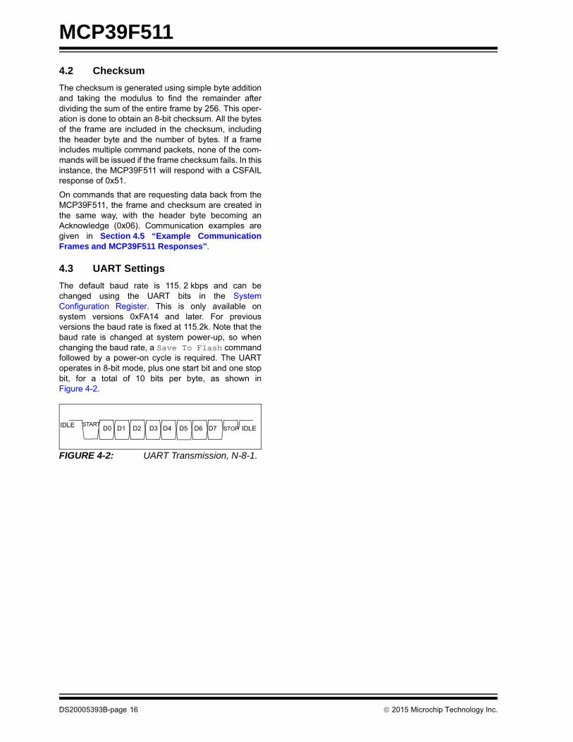
The default baud rate is 115. 2 kbps and can bechanged using the UART bits in the SystemConfiguration Register. This is only available onsystem versions 0xFA14 and later. For previousversions the baud rate is fixed at 115.2k. Note that thebaud rate is changed at system power-up, so whenchanging the baud rate, a Save To Flash commandfollowed by a power-on cycle is required. The UARToperates in 8-bit mode, plus one start bit and one stopbit, for a total of 10 bits per byte, as shown inFigure 4-2.
FIGURE 4-2: UART Transmission, N-8-1.
IDLE STARTIDLESTOPD0 D1 D2 D3 D4 D5 D6 D7
2015 Microchip Technology Inc. DS20005393B-page 17
MCP39F511
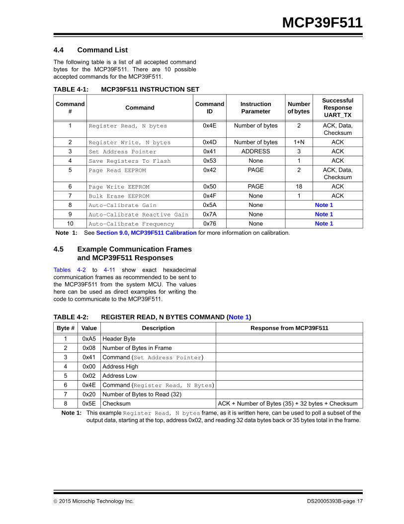
4.4 Command List
The following table is a list of all accepted commandbytes for the MCP39F511. There are 10 possibleaccepted commands for the MCP39F511.
4.5 Example Communication Frames and MCP39F511 Responses
Tables 4-2 to 4-11 show exact hexadecimalcommunication frames as recommended to be sent tothe MCP39F511 from the system MCU. The valueshere can be used as direct examples for writing thecode to communicate to the MCP39F511.
TABLE 4-1: MCP39F511 INSTRUCTION SET
Command #
CommandCommand
ID Instruction Parameter
Number of bytes
Successful Response UART_TX
1 Register Read, N bytes 0x4E Number of bytes 2 ACK, Data, Checksum
2 Register Write, N bytes 0x4D Number of bytes 1+N ACK
3 Set Address Pointer 0x41 ADDRESS 3 ACK
4 Save Registers To Flash 0x53 None 1 ACK
5 Page Read EEPROM 0x42 PAGE 2 ACK, Data, Checksum
6 Page Write EEPROM 0x50 PAGE 18 ACK
7 Bulk Erase EEPROM 0x4F None 1 ACK
8 Auto-Calibrate Gain 0x5A None Note 1
9 Auto-Calibrate Reactive Gain 0x7A None Note 1
10 Auto-Calibrate Frequency 0x76 None Note 1
Note 1: See Section 9.0, MCP39F511 Calibration for more information on calibration.
TABLE 4-2: REGISTER READ, N BYTES COMMAND (Note 1)
Byte # Value Description Response from MCP39F511
1 0xA5 Header Byte
2 0x08 Number of Bytes in Frame
3 0x41 Command (Set Address Pointer)
4 0x00 Address High
5 0x02 Address Low
6 0x4E Command (Register Read, N Bytes)
7 0x20 Number of Bytes to Read (32)
8 0x5E Checksum ACK + Number of Bytes (35) + 32 bytes + Checksum
Note 1: This example Register Read, N bytes frame, as it is written here, can be used to poll a subset of theoutput data, starting at the top, address 0x02, and reading 32 data bytes back or 35 bytes total in the frame.
MCP39F511
DS20005393B-page 18 2015 Microchip Technology Inc.
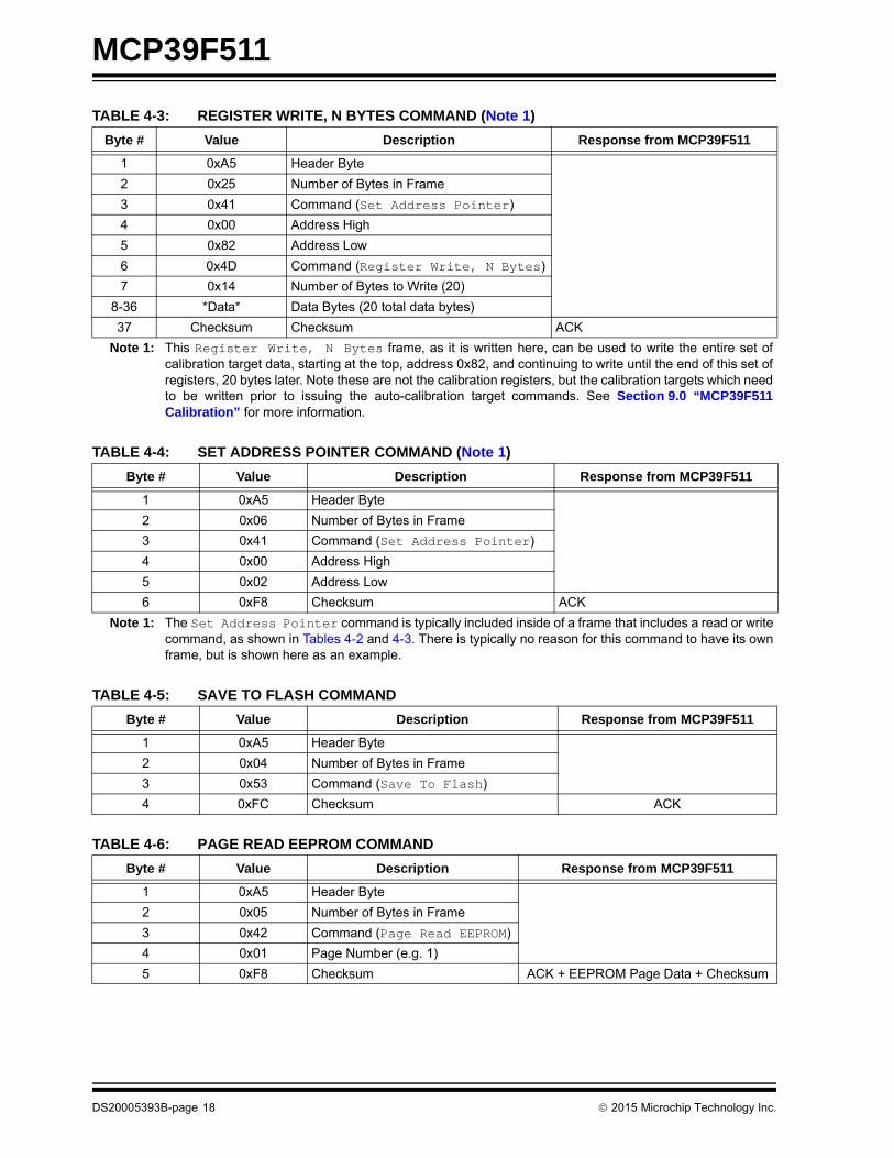
TABLE 4-3: REGISTER WRITE, N BYTES COMMAND (Note 1)
Byte # Value Description Response from MCP39F511
1 0xA5 Header Byte
2 0x25 Number of Bytes in Frame
3 0x41 Command (Set Address Pointer)
4 0x00 Address High
5 0x82 Address Low
6 0x4D Command (Register Write, N Bytes)
7 0x14 Number of Bytes to Write (20)
8-36 *Data* Data Bytes (20 total data bytes)
37 Checksum Checksum ACK
Note 1: This Register Write, N Bytes frame, as it is written here, can be used to write the entire set ofcalibration target data, starting at the top, address 0x82, and continuing to write until the end of this set ofregisters, 20 bytes later. Note these are not the calibration registers, but the calibration targets which needto be written prior to issuing the auto-calibration target commands. See Section 9.0 “MCP39F511Calibration” for more information.
TABLE 4-4: SET ADDRESS POINTER COMMAND (Note 1)
Byte # Value Description Response from MCP39F511
1 0xA5 Header Byte
2 0x06 Number of Bytes in Frame
3 0x41 Command (Set Address Pointer)
4 0x00 Address High
5 0x02 Address Low
6 0xF8 Checksum ACK
Note 1: The Set Address Pointer command is typically included inside of a frame that includes a read or writecommand, as shown in Tables 4-2 and 4-3. There is typically no reason for this command to have its ownframe, but is shown here as an example.
TABLE 4-5: SAVE TO FLASH COMMAND
Byte # Value Description Response from MCP39F511
1 0xA5 Header Byte
2 0x04 Number of Bytes in Frame
3 0x53 Command (Save To Flash)
4 0xFC Checksum ACK
TABLE 4-6: PAGE READ EEPROM COMMAND
Byte # Value Description Response from MCP39F511
1 0xA5 Header Byte
2 0x05 Number of Bytes in Frame
3 0x42 Command (Page Read EEPROM)
4 0x01 Page Number (e.g. 1)
5 0xF8 Checksum ACK + EEPROM Page Data + Checksum
2015 Microchip Technology Inc. DS20005393B-page 19
MCP39F511
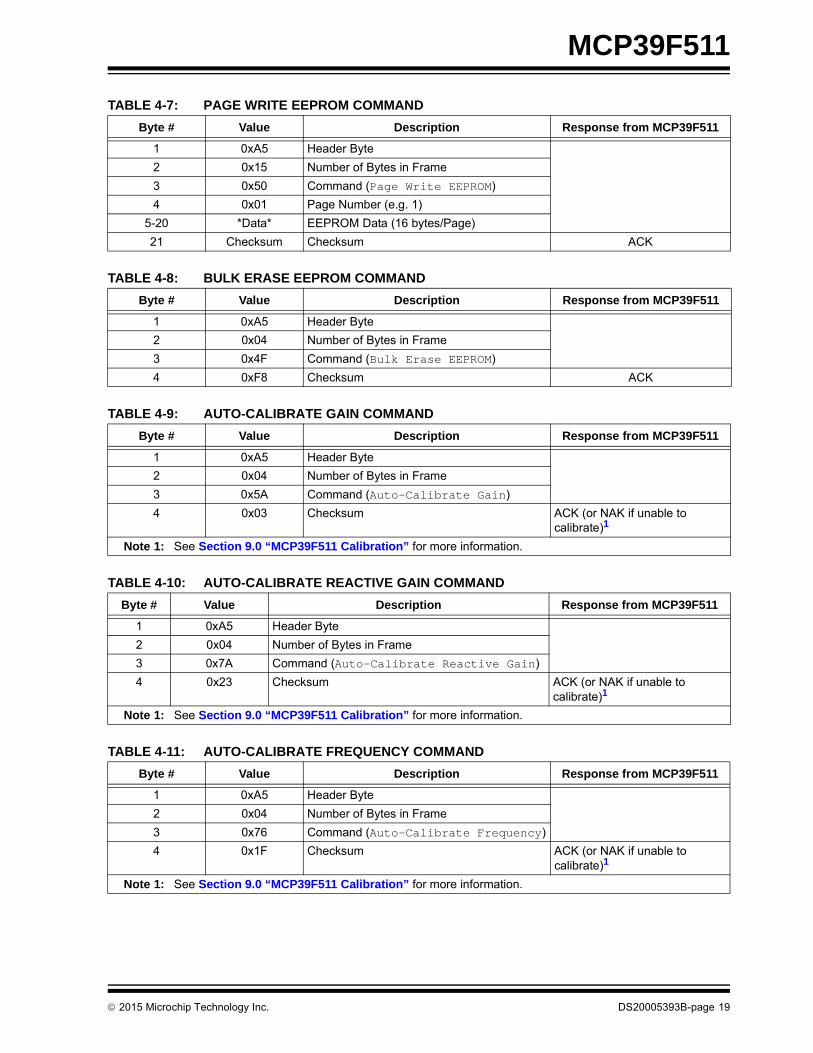
TABLE 4-7: PAGE WRITE EEPROM COMMAND
Byte # Value Description Response from MCP39F511
1 0xA5 Header Byte
2 0x15 Number of Bytes in Frame
3 0x50 Command (Page Write EEPROM)
4 0x01 Page Number (e.g. 1)
5-20 *Data* EEPROM Data (16 bytes/Page)
21 Checksum Checksum ACK
TABLE 4-8: BULK ERASE EEPROM COMMAND
Byte # Value Description Response from MCP39F511
1 0xA5 Header Byte
2 0x04 Number of Bytes in Frame
3 0x4F Command (Bulk Erase EEPROM)
4 0xF8 Checksum ACK
TABLE 4-9: AUTO-CALIBRATE GAIN COMMAND
Byte # Value Description Response from MCP39F511
1 0xA5 Header Byte
2 0x04 Number of Bytes in Frame
3 0x5A Command (Auto-Calibrate Gain)
4 0x03 Checksum ACK (or NAK if unable to calibrate)1
Note 1: See Section 9.0 “MCP39F511 Calibration” for more information.
TABLE 4-10: AUTO-CALIBRATE REACTIVE GAIN COMMAND
Byte # Value Description Response from MCP39F511
1 0xA5 Header Byte
2 0x04 Number of Bytes in Frame
3 0x7A Command (Auto-Calibrate Reactive Gain)
4 0x23 Checksum ACK (or NAK if unable to calibrate)1
Note 1: See Section 9.0 “MCP39F511 Calibration” for more information.
TABLE 4-11: AUTO-CALIBRATE FREQUENCY COMMAND
Byte # Value Description Response from MCP39F511
1 0xA5 Header Byte
2 0x04 Number of Bytes in Frame
3 0x76 Command (Auto-Calibrate Frequency)
4 0x1F Checksum ACK (or NAK if unable to calibrate)1
Note 1: See Section 9.0 “MCP39F511 Calibration” for more information.
MCP39F511
DS20005393B-page 20 2015 Microchip Technology Inc.
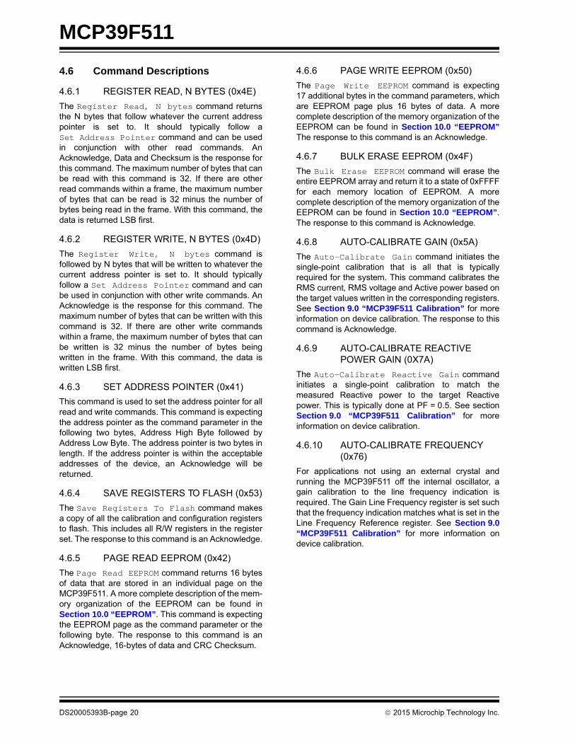
4.6 Command Descriptions
4.6.1 REGISTER READ, N BYTES (0x4E)
The Register Read, N bytes command returnsthe N bytes that follow whatever the current addresspointer is set to. It should typically follow aSet Address Pointer command and can be usedin conjunction with other read commands. AnAcknowledge, Data and Checksum is the response forthis command. The maximum number of bytes that canbe read with this command is 32. If there are otherread commands within a frame, the maximum numberof bytes that can be read is 32 minus the number ofbytes being read in the frame. With this command, thedata is returned LSB first.
4.6.2 REGISTER WRITE, N BYTES (0x4D)
The Register Write, N bytes command isfollowed by N bytes that will be written to whatever thecurrent address pointer is set to. It should typicallyfollow a Set Address Pointer command and canbe used in conjunction with other write commands. AnAcknowledge is the response for this command. Themaximum number of bytes that can be written with thiscommand is 32. If there are other write commandswithin a frame, the maximum number of bytes that canbe written is 32 minus the number of bytes beingwritten in the frame. With this command, the data iswritten LSB first.
4.6.3 SET ADDRESS POINTER (0x41)
This command is used to set the address pointer for allread and write commands. This command is expectingthe address pointer as the command parameter in thefollowing two bytes, Address High Byte followed byAddress Low Byte. The address pointer is two bytes inlength. If the address pointer is within the acceptableaddresses of the device, an Acknowledge will bereturned.
4.6.4 SAVE REGISTERS TO FLASH (0x53)
The Save Registers To Flash command makesa copy of all the calibration and configuration registersto flash. This includes all R/W registers in the registerset. The response to this command is an Acknowledge.
4.6.5 PAGE READ EEPROM (0x42)
The Page Read EEPROM command returns 16 bytesof data that are stored in an individual page on theMCP39F511. A more complete description of the mem-ory organization of the EEPROM can be found inSection 10.0 “EEPROM”. This command is expectingthe EEPROM page as the command parameter or thefollowing byte. The response to this command is anAcknowledge, 16-bytes of data and CRC Checksum.
4.6.6 PAGE WRITE EEPROM (0x50)
The Page Write EEPROM command is expecting17 additional bytes in the command parameters, whichare EEPROM page plus 16 bytes of data. A morecomplete description of the memory organization of theEEPROM can be found in Section 10.0 “EEPROM”The response to this command is an Acknowledge.
4.6.7 BULK ERASE EEPROM (0x4F)
The Bulk Erase EEPROM command will erase theentire EEPROM array and return it to a state of 0xFFFFfor each memory location of EEPROM. A morecomplete description of the memory organization of theEEPROM can be found in Section 10.0 “EEPROM”.The response to this command is Acknowledge.
4.6.8 AUTO-CALIBRATE GAIN (0x5A)
The Auto-Calibrate Gain command initiates thesingle-point calibration that is all that is typicallyrequired for the system. This command calibrates theRMS current, RMS voltage and Active power based onthe target values written in the corresponding registers.See Section 9.0 “MCP39F511 Calibration” for moreinformation on device calibration. The response to thiscommand is Acknowledge.
4.6.9 AUTO-CALIBRATE REACTIVE POWER GAIN (0X7A)
The Auto-Calibrate Reactive Gain commandinitiates a single-point calibration to match themeasured Reactive power to the target Reactivepower. This is typically done at PF = 0.5. See sectionSection 9.0 “MCP39F511 Calibration” for moreinformation on device calibration.
4.6.10 AUTO-CALIBRATE FREQUENCY (0x76)
For applications not using an external crystal andrunning the MCP39F511 off the internal oscillator, again calibration to the line frequency indication isrequired. The Gain Line Frequency register is set suchthat the frequency indication matches what is set in theLine Frequency Reference register. See Section 9.0“MCP39F511 Calibration” for more information ondevice calibration.
2015 Microchip Technology Inc. DS20005393B-page 21
MCP39F511
4.7 Notation for Register Types
The following notation has been adopted for describingthe various registers used in the MCP39F511:
4.8 Single-Wire Transmission Mode
In Single-Wire Transmission mode, at the end of eachcomputation cycle, the device automatically transmits aframe of power data. This allows for single-wire com-munication after the device has been configured.
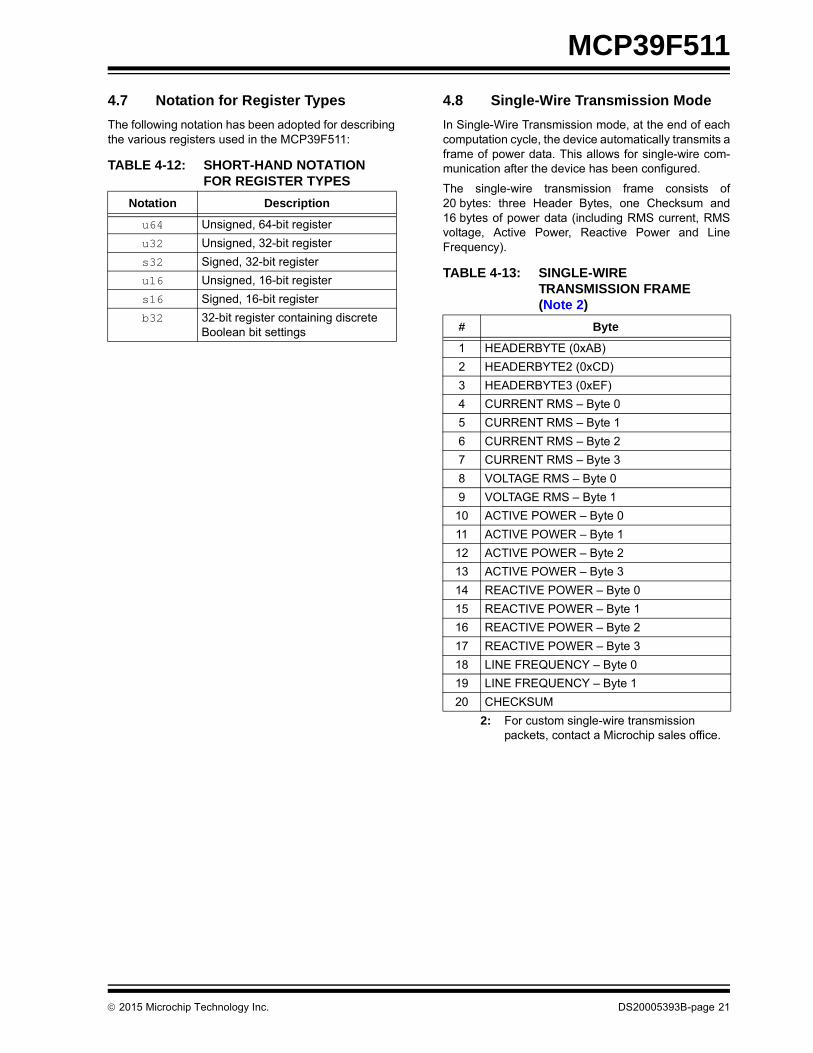
The single-wire transmission frame consists of20 bytes: three Header Bytes, one Checksum and16 bytes of power data (including RMS current, RMSvoltage, Active Power, Reactive Power and LineFrequency).
TABLE 4-12: SHORT-HAND NOTATION FOR REGISTER TYPES
Notation Description
u64 Unsigned, 64-bit register
u32 Unsigned, 32-bit register
s32 Signed, 32-bit register
u16 Unsigned, 16-bit register
s16 Signed, 16-bit register
b32 32-bit register containing discrete Boolean bit settings
TABLE 4-13: SINGLE-WIRE TRANSMISSION FRAME (Note 2)
# Byte
1 HEADERBYTE (0xAB)
2 HEADERBYTE2 (0xCD)
3 HEADERBYTE3 (0xEF)
4 CURRENT RMS – Byte 0
5 CURRENT RMS – Byte 1
6 CURRENT RMS – Byte 2
7 CURRENT RMS – Byte 3
8 VOLTAGE RMS – Byte 0
9 VOLTAGE RMS – Byte 1
10 ACTIVE POWER – Byte 0
11 ACTIVE POWER – Byte 1
12 ACTIVE POWER – Byte 2
13 ACTIVE POWER – Byte 3
14 REACTIVE POWER – Byte 0
15 REACTIVE POWER – Byte 1
16 REACTIVE POWER – Byte 2
17 REACTIVE POWER – Byte 3
18 LINE FREQUENCY – Byte 0
19 LINE FREQUENCY – Byte 1
20 CHECKSUM
2: For custom single-wire transmission packets, contact a Microchip sales office.

MCP39F511
DS20005393B-page 22 2015 Microchip Technology Inc.
NOTES:
2015 Microchip Technology Inc. DS20005393B-page 23
MCP39F511
5.0 CALCULATION ENGINE (CE) DESCRIPTION
5.1 Computation Cycle Overview
The MCP39F511 uses a coherent sampling algorithmto phase lock the sampling rate to the line frequencywith an integer number of samples per line cycle, andreports all power output quantities at a 2N number ofline cycles. This is defined as a computation cycle andis dependent on the line frequency, so any change inthe line frequency will change the update rate of thepower outputs.
5.2 Accumulation Interval Parameter
The accumulation interval is defined as an 2N numberof line cycles, where N is the value in the AccumulationInterval Parameter register.
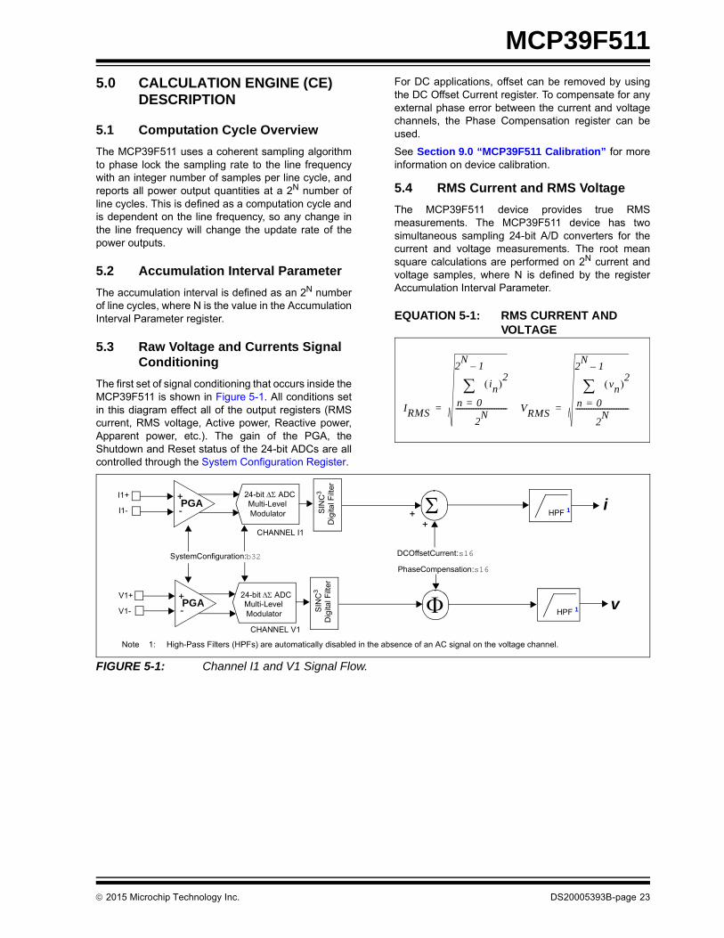
5.3 Raw Voltage and Currents Signal Conditioning
The first set of signal conditioning that occurs inside theMCP39F511 is shown in Figure 5-1. All conditions setin this diagram effect all of the output registers (RMScurrent, RMS voltage, Active power, Reactive power,Apparent power, etc.). The gain of the PGA, theShutdown and Reset status of the 24-bit ADCs are allcontrolled through the System Configuration Register.
For DC applications, offset can be removed by usingthe DC Offset Current register. To compensate for anyexternal phase error between the current and voltagechannels, the Phase Compensation register can beused.
See Section 9.0 “MCP39F511 Calibration” for moreinformation on device calibration.
5.4 RMS Current and RMS Voltage
The MCP39F511 device provides true RMSmeasurements. The MCP39F511 device has twosimultaneous sampling 24-bit A/D converters for thecurrent and voltage measurements. The root meansquare calculations are performed on 2N current andvoltage samples, where N is defined by the registerAccumulation Interval Parameter.
EQUATION 5-1: RMS CURRENT AND VOLTAGE
FIGURE 5-1: Channel I1 and V1 Signal Flow.
IRMS
in 2
n 0=
2N
1–
2N
-----------------------------= VRMS
vn 2
n 0=
2N
1–
2N
------------------------------=
CHANNEL I1
SIN
C3
Dig
ital F
ilter
24-bit ADC Multi-LevelModulator
DCOffsetCurrent:s16
++
CHANNEL V1
SIN
C3
Dig
ital F
ilter
24-bit ADC Multi-LevelModulator HPF 1
PhaseCompensation:s16
HPF 1
+-PGA
I1+
I1-
+-PGA
V1+
V1-
SystemConfiguration:b32
i
v
Note 1: High-Pass Filters (HPFs) are automatically disabled in the absence of an AC signal on the voltage channel.
MCP39F511
DS20005393B-page 24 2015 Microchip Technology Inc.
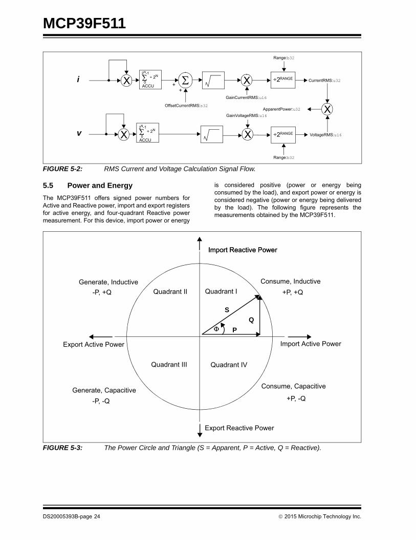
FIGURE 5-2: RMS Current and Voltage Calculation Signal Flow.
5.5 Power and Energy
The MCP39F511 offers signed power numbers forActive and Reactive power, import and export registersfor active energy, and four-quadrant Reactive powermeasurement. For this device, import power or energy
is considered positive (power or energy beingconsumed by the load), and export power or energy isconsidered negative (power or energy being deliveredby the load). The following figure represents themeasurements obtained by the MCP39F511.
FIGURE 5-3: The Power Circle and Triangle (S = Apparent, P = Active, Q = Reactive).
OffsetCurrentRMS:s32
X CurrentRMS:u32+
+
Range:b32
X
÷2RANGE
VoltageRMS:u16
Range:b32
XApparentPower:u32
i
v
ACCU0
2N-1÷ 2N
ACCU0
2N-1÷ 2N
GainCurrentRMS:u16
X
X
GainVoltageRMS:u16
÷2RANGE
P
S
Q
Quadrant IQuadrant II
Quadrant IVQuadrant III
Import Active PowerExport Active Power
Import Reactive PowerImport Reactive Power
Export Reactive Power
Consume, Inductive
Consume, Capacitive
Generate, Inductive
Generate, Capacitive
-P, +Q +P, +Q
+P, -Q-P, -Q
2015 Microchip Technology Inc. DS20005393B-page 25
MCP39F511
5.6 Energy Accumulation
Energy accumulation for all four energy registers(import/export, active/reactive) occurs at the end ofeach computation cycle, if the energy accumulationhas been turned on. See Section 6.3 “System StatusRegister” on the energy control register. A no-loadthreshold test is done to make sure the measuredenergy is not below the no-load threshold, if it is above,the accumulation occurs with a default energyresolution of 1mWh for all of the energy registers.
5.6.1 NO-LOAD THRESHOLD
The no-load threshold is set by modifying the value inthe No-Load Threshold register. The unit for thisregister is power with a default resolution of 0.01W. Thedefault value is 100 or 1.00W. Any power that is below1W will not be accumulated into any of the energyregisters.
5.7 Apparent Power (S)
This 32-bit register is the output register for the finalApparent power indication. It is the product of RMScurrent and RMS voltage as shown in Equation 5-2.
EQUATION 5-2: APPARENT POWER (S)
For scaling of the Apparent power indication, the calcu-lation engine uses the register Apparent Power Divisor.This is described in the following register operations,per Equation 5-3.
EQUATION 5-3: APPARENT POWER (S)
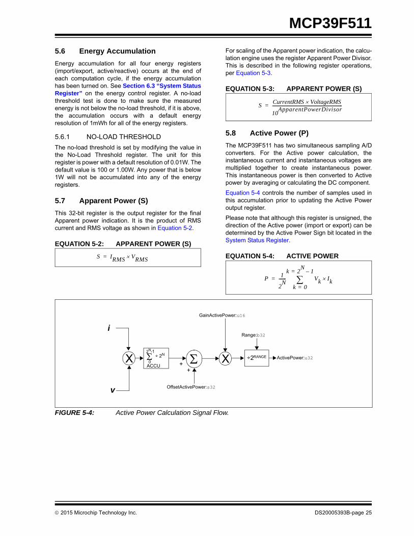
5.8 Active Power (P)
The MCP39F511 has two simultaneous sampling A/Dconverters. For the Active power calculation, theinstantaneous current and instantaneous voltages aremultiplied together to create instantaneous power.This instantaneous power is then converted to Activepower by averaging or calculating the DC component.
Equation 5-4 controls the number of samples used inthis accumulation prior to updating the Active Poweroutput register.
Please note that although this register is unsigned, thedirection of the Active power (import or export) can bedetermined by the Active Power Sign bit located in theSystem Status Register.
EQUATION 5-4: ACTIVE POWER
FIGURE 5-4: Active Power Calculation Signal Flow.
S IRMS VRMS=
SCurrentRMS VoltageRMS
10ApparentPowerDivisor
---------------------------------------------------------------------=
P1
2N
------- Vk Ikk 0=
k 2N
1–=
=
OffsetActivePower:s32
X ActivePower:u32+
+
X
GainActivePower:u16
Range:b32
ACCU0
2N-1÷ 2N
÷2RANGE
i
v
MCP39F511
DS20005393B-page 26 2015 Microchip Technology Inc.
5.9 Power Factor (PF)
Power factor is calculated by the ratio of P to S orActive power divided by Apparent power.
EQUATION 5-5: POWER FACTOR
The Power Factor Reading is stored in a signed 16-bitregister (Power Factor). This register is a signed, 2'scomplement register with the MSB representing thepolarity of the power factor. A positive power factormeans Active power is being imported, negative powerfactor represents export Active power. The sign of thereactive power component is used to tell if the currentis lagging the voltage, with a positive sign meaning aninductive load, and a negative sign meaning capacitive.Each LSB is then equivalent to a weight of 2-15. Amaximum register value of 0x7FFF corresponds to apower factor of 1. The minimum register value of0x8000 corresponds to a power factor of -1.
5.10 Reactive Power (Q)
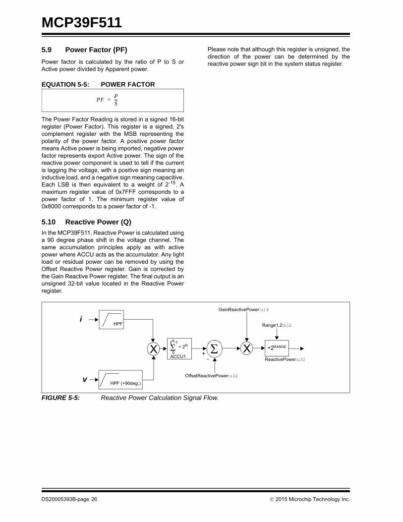
In the MCP39F511, Reactive Power is calculated usinga 90 degree phase shift in the voltage channel. Thesame accumulation principles apply as with activepower where ACCU acts as the accumulator. Any lightload or residual power can be removed by using theOffset Reactive Power register. Gain is corrected bythe Gain Reactive Power register. The final output is anunsigned 32-bit value located in the Reactive Powerregister.
Please note that although this register is unsigned, thedirection of the power can be determined by thereactive power sign bit in the system status register.
FIGURE 5-5: Reactive Power Calculation Signal Flow.
PFPS---=
OffsetReactivePower:s32
XACCU10
HPF
ReactivePower:u32+
-
HPF (+90deg.)
X
GainReactivePower:u16
Range1,2:b32
2N-1÷ 2N ÷2RANGE
i
v
2015 Microchip Technology Inc. DS20005393B-page 27
MCP39F511
5.11 10-Bit Analog Input
The least 10 significant bits of the 16-bit Analog Inputregister contain the output of the 10-bit ADC. Theconversion rate of the analog input occurs once everycomputation cycle.
The Thermistor Voltage can be used for temperaturecompensation of the calculation engine. SeeSection 9.7 “Temperature Compensation” for moreinformation.
FIGURE 5-6: Using an Analog Out-Temperature Sensor for Automatic Temperature Compensation.
5.12 Minimum and Maximum Recordings
The MCP39F511 has the ability to record minimum andmaximum outputs and keep them in a total of fourregisters (two minimum and two maximum) based onthe value of address pointers located in the fourregisters listed in this section.
A minimum and maximum test is done after eachcalculation interval. If the current measurement valueof the value directed to by the pointer is smaller orlarger than the value in the Minimum or Maximumregister, the record is updated appropriately.
The registers are:
• MinMaxPointer1 → MinimumRecord1, Maximum-Record1
• MinMaxPointer2 → MinimumRecord2, Maximum-Record2
Only the Output Quantity register addresses can betracked by the Min/Max pointers. Output Quantityregisters are defined as those from Voltage RMS toApparent Power (addresses 0x0006 to 0x001A). Allother addresses will be ignored by the calculationengine.
Please note that the 64-bit energy registers can not betracked through the Minimum and Maximum Recordingregisters.
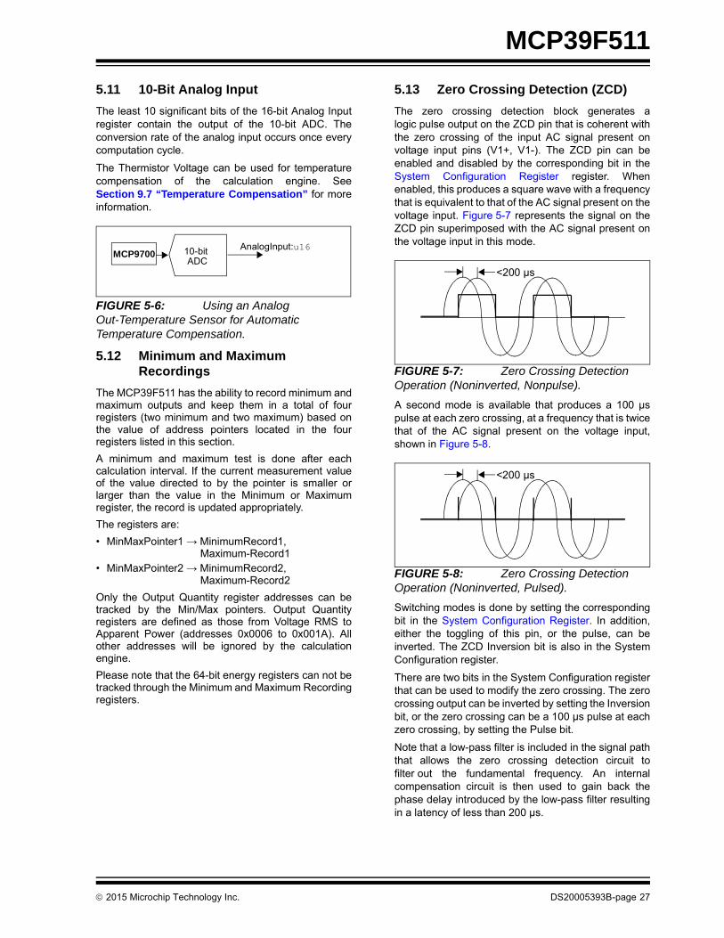
5.13 Zero Crossing Detection (ZCD)
The zero crossing detection block generates alogic pulse output on the ZCD pin that is coherent withthe zero crossing of the input AC signal present onvoltage input pins (V1+, V1-). The ZCD pin can beenabled and disabled by the corresponding bit in theSystem Configuration Register register. Whenenabled, this produces a square wave with a frequencythat is equivalent to that of the AC signal present on thevoltage input. Figure 5-7 represents the signal on theZCD pin superimposed with the AC signal present onthe voltage input in this mode.
FIGURE 5-7: Zero Crossing Detection Operation (Noninverted, Nonpulse).
A second mode is available that produces a 100 µspulse at each zero crossing, at a frequency that is twicethat of the AC signal present on the voltage input,shown in Figure 5-8.
FIGURE 5-8: Zero Crossing Detection Operation (Noninverted, Pulsed).
Switching modes is done by setting the correspondingbit in the System Configuration Register. In addition,either the toggling of this pin, or the pulse, can beinverted. The ZCD Inversion bit is also in the SystemConfiguration register.
There are two bits in the System Configuration registerthat can be used to modify the zero crossing. The zerocrossing output can be inverted by setting the Inversionbit, or the zero crossing can be a 100 µs pulse at eachzero crossing, by setting the Pulse bit.
Note that a low-pass filter is included in the signal paththat allows the zero crossing detection circuit tofilter out the fundamental frequency. An internalcompensation circuit is then used to gain back thephase delay introduced by the low-pass filter resultingin a latency of less than 200 µs.
AnalogInput:u1610-bit ADC
MCP9700
<200 µs
<200 µs

MCP39F511
DS20005393B-page 28 2015 Microchip Technology Inc.
NOTES:
2015 Microchip Technology Inc. DS20005393B-page 29
MCP39F511
6.0 REGISTER DESCRIPTIONS
6.1 Complete Register Map
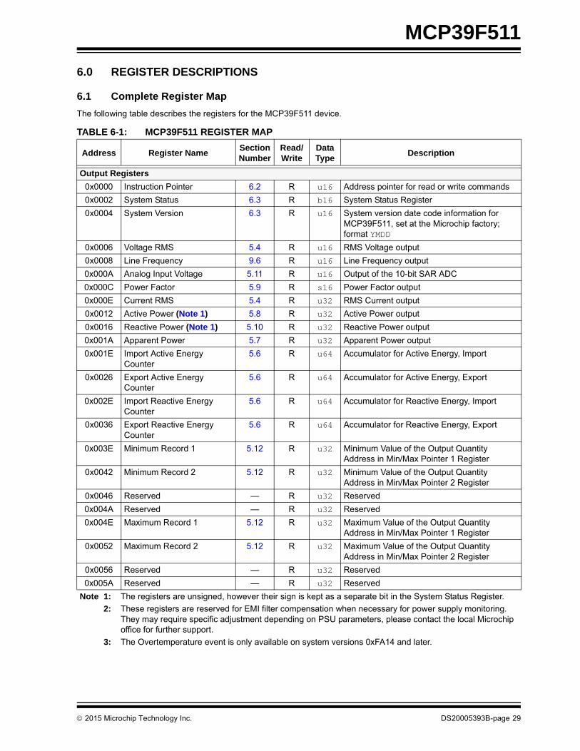
The following table describes the registers for the MCP39F511 device.
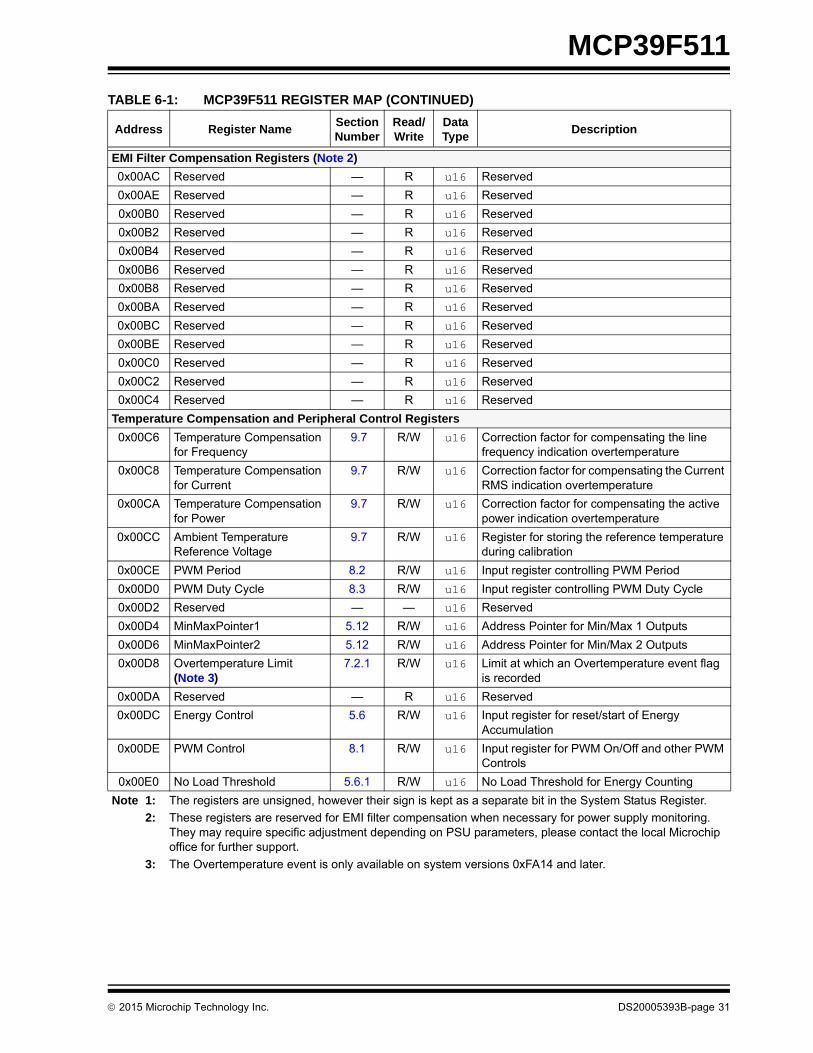
TABLE 6-1: MCP39F511 REGISTER MAP
Address Register NameSection Number
Read/Write
Data Type
Description
Output Registers
0x0000 Instruction Pointer 6.2 R u16 Address pointer for read or write commands
0x0002 System Status 6.3 R b16 System Status Register
0x0004 System Version 6.3 R u16 System version date code information for MCP39F511, set at the Microchip factory; format YMDD
0x0006 Voltage RMS 5.4 R u16 RMS Voltage output
0x0008 Line Frequency 9.6 R u16 Line Frequency output
0x000A Analog Input Voltage 5.11 R u16 Output of the 10-bit SAR ADC
0x000C Power Factor 5.9 R s16 Power Factor output
0x000E Current RMS 5.4 R u32 RMS Current output
0x0012 Active Power (Note 1) 5.8 R u32 Active Power output
0x0016 Reactive Power (Note 1) 5.10 R u32 Reactive Power output
0x001A Apparent Power 5.7 R u32 Apparent Power output
0x001E Import Active Energy Counter
5.6 R u64 Accumulator for Active Energy, Import
0x0026 Export Active Energy Counter
5.6 R u64 Accumulator for Active Energy, Export
0x002E Import Reactive Energy Counter
5.6 R u64 Accumulator for Reactive Energy, Import
0x0036 Export Reactive Energy Counter
5.6 R u64 Accumulator for Reactive Energy, Export
0x003E Minimum Record 1 5.12 R u32 Minimum Value of the Output Quantity Address in Min/Max Pointer 1 Register
0x0042 Minimum Record 2 5.12 R u32 Minimum Value of the Output Quantity Address in Min/Max Pointer 2 Register
0x0046 Reserved — R u32 Reserved
0x004A Reserved — R u32 Reserved
0x004E Maximum Record 1 5.12 R u32 Maximum Value of the Output Quantity Address in Min/Max Pointer 1 Register
0x0052 Maximum Record 2 5.12 R u32 Maximum Value of the Output Quantity Address in Min/Max Pointer 2 Register
0x0056 Reserved — R u32 Reserved
0x005A Reserved — R u32 Reserved
Note 1: The registers are unsigned, however their sign is kept as a separate bit in the System Status Register.
2: These registers are reserved for EMI filter compensation when necessary for power supply monitoring. They may require specific adjustment depending on PSU parameters, please contact the local Microchip office for further support.
3: The Overtemperature event is only available on system versions 0xFA14 and later.
MCP39F511
DS20005393B-page 30 2015 Microchip Technology Inc.
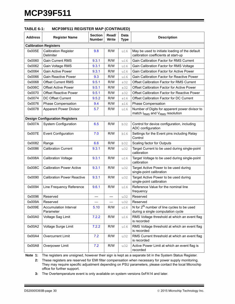
Calibration Registers
0x005E Calibration Register Delimiter
9.8 R/W u16 May be used to initiate loading of the default calibration coefficients at start-up
0x0060 Gain Current RMS 9.3.1 R/W u16 Gain Calibration Factor for RMS Current
0x0062 Gain Voltage RMS 9.3.1 R/W u16 Gain Calibration Factor for RMS Voltage
0x0064 Gain Active Power 9.3.1 R/W u16 Gain Calibration Factor for Active Power
0x0066 Gain Reactive Power 9.3 R/W u16 Gain Calibration Factor for Reactive Power
0x0068 Offset Current RMS 9.5.1 R/W s32 Offset Calibration Factor for RMS Current
0x006C Offset Active Power 9.5.1 R/W s32 Offset Calibration Factor for Active Power
0x0070 Offset Reactive Power 9.5.1 R/W s32 Offset Calibration Factor for Reactive Power
0x0074 DC Offset Current 9.5.2 R/W s16 Offset Calibration Factor for DC Current
0x0076 Phase Compensation 9.4 R/W s16 Phase Compensation
0x0078 Apparent Power Divisor 5.7 R/W u16 Number of Digits for apparent power divisor to match IRMS and VRMS resolution
Design Configuration Registers
0x007A System Configuration 6.5 R/W b32 Control for device configuration, including ADC configuration
0x007E Event Configuration 7.0 R/W b16 Settings for the Event pins including Relay Control
0x0082 Range 6.6 R/W b32 Scaling factor for Outputs
0x0086 Calibration Current 9.3.1 R/W u32 Target Current to be used during single-point calibration
0x008A Calibration Voltage 9.3.1 R/W u16 Target Voltage to be used during single-point calibration
0x008C Calibration Power Active 9.3.1 R/W u32 Target Active Power to be used during single-point calibration
0x0090 Calibration Power Reactive 9.3.1 R/W u32 Target Active Power to be used during single-point calibration
0x0094 Line Frequency Reference 9.6.1 R/W u16 Reference Value for the nominal line frequency
0x0096 Reserved — — u32 Reserved
0x009A Reserved — — u32 Reserved
0x009E Accumulation Interval Parameter
5.10 R/W u16 N for 2N number of line cycles to be used during a single computation cycle
0x00A0 Voltage Sag Limit 7.2.2 R/W u16 RMS Voltage threshold at which an event flag is recorded
0x00A2 Voltage Surge Limit 7.2.2 R/W u16 RMS Voltage threshold at which an event flag is recorded
0x00A4 Overcurrent Limit 7.2 R/W u32 RMS Current threshold at which an event flag is recorded
0x00A8 Overpower Limit 7.2 R/W u32 Active Power Limit at which an event flag is recorded
TABLE 6-1: MCP39F511 REGISTER MAP (CONTINUED)
Address Register NameSection Number
Read/Write
Data Type
Description
Note 1: The registers are unsigned, however their sign is kept as a separate bit in the System Status Register.
2: These registers are reserved for EMI filter compensation when necessary for power supply monitoring. They may require specific adjustment depending on PSU parameters, please contact the local Microchip office for further support.
3: The Overtemperature event is only available on system versions 0xFA14 and later.
2015 Microchip Technology Inc. DS20005393B-page 31
MCP39F511
EMI Filter Compensation Registers (Note 2)
0x00AC Reserved — R u16 Reserved
0x00AE Reserved — R u16 Reserved
0x00B0 Reserved — R u16 Reserved
0x00B2 Reserved — R u16 Reserved
0x00B4 Reserved — R u16 Reserved
0x00B6 Reserved — R u16 Reserved
0x00B8 Reserved — R u16 Reserved
0x00BA Reserved — R u16 Reserved
0x00BC Reserved — R u16 Reserved
0x00BE Reserved — R u16 Reserved
0x00C0 Reserved — R u16 Reserved
0x00C2 Reserved — R u16 Reserved
0x00C4 Reserved — R u16 Reserved
Temperature Compensation and Peripheral Control Registers
0x00C6 Temperature Compensation for Frequency
9.7 R/W u16 Correction factor for compensating the line frequency indication overtemperature
0x00C8 Temperature Compensation for Current
9.7 R/W u16 Correction factor for compensating the Current RMS indication overtemperature
0x00CA Temperature Compensation for Power
9.7 R/W u16 Correction factor for compensating the active power indication overtemperature
0x00CC Ambient Temperature Reference Voltage
9.7 R/W u16 Register for storing the reference temperature during calibration
0x00CE PWM Period 8.2 R/W u16 Input register controlling PWM Period
0x00D0 PWM Duty Cycle 8.3 R/W u16 Input register controlling PWM Duty Cycle
0x00D2 Reserved — — u16 Reserved
0x00D4 MinMaxPointer1 5.12 R/W u16 Address Pointer for Min/Max 1 Outputs
0x00D6 MinMaxPointer2 5.12 R/W u16 Address Pointer for Min/Max 2 Outputs
0x00D8 Overtemperature Limit (Note 3)
7.2.1 R/W u16 Limit at which an Overtemperature event flag is recorded
0x00DA Reserved — R u16 Reserved
0x00DC Energy Control 5.6 R/W u16 Input register for reset/start of Energy Accumulation
0x00DE PWM Control 8.1 R/W u16 Input register for PWM On/Off and other PWM Controls
0x00E0 No Load Threshold 5.6.1 R/W u16 No Load Threshold for Energy Counting
TABLE 6-1: MCP39F511 REGISTER MAP (CONTINUED)
Address Register NameSection Number
Read/Write
Data Type
Description
Note 1: The registers are unsigned, however their sign is kept as a separate bit in the System Status Register.
2: These registers are reserved for EMI filter compensation when necessary for power supply monitoring. They may require specific adjustment depending on PSU parameters, please contact the local Microchip office for further support.
3: The Overtemperature event is only available on system versions 0xFA14 and later.
MCP39F511
DS20005393B-page 32 2015 Microchip Technology Inc.
6.2 Address Pointer Register
This unsigned 16-bit register contains the address towhich all read and write instructions occur. This registeris only written through the Set Address Pointercommand and is otherwise outside the writable rangeof register addresses.
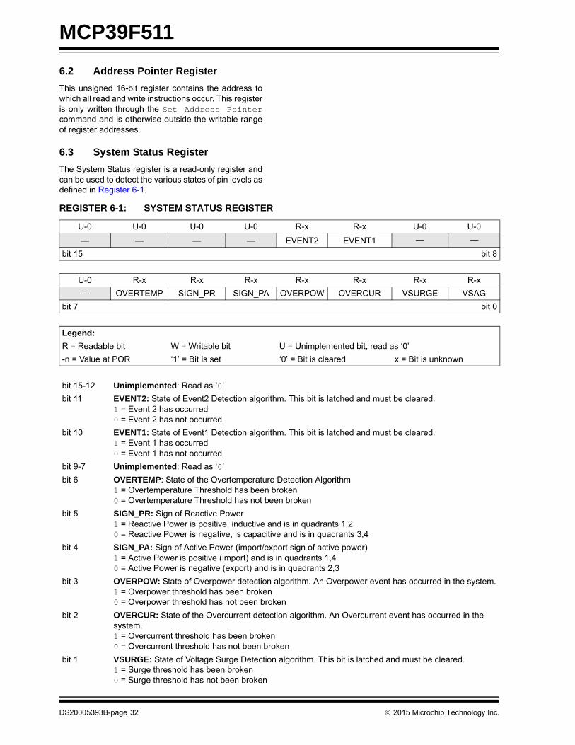
6.3 System Status Register
The System Status register is a read-only register andcan be used to detect the various states of pin levels asdefined in Register 6-1.
REGISTER 6-1: SYSTEM STATUS REGISTER
U-0 U-0 U-0 U-0 R-x R-x U-0 U-0
— — — — EVENT2 EVENT1 — —
bit 15 bit 8
U-0 R-x R-x R-x R-x R-x R-x R-x
— OVERTEMP SIGN_PR SIGN_PA OVERPOW OVERCUR VSURGE VSAG
bit 7 bit 0
Legend:
R = Readable bit W = Writable bit U = Unimplemented bit, read as ‘0’
-n = Value at POR ‘1’ = Bit is set ‘0’ = Bit is cleared x = Bit is unknown
bit 15-12 Unimplemented: Read as ‘0’
bit 11 EVENT2: State of Event2 Detection algorithm. This bit is latched and must be cleared.1 = Event 2 has occurred0 = Event 2 has not occurred
bit 10 EVENT1: State of Event1 Detection algorithm. This bit is latched and must be cleared.1 = Event 1 has occurred0 = Event 1 has not occurred
bit 9-7 Unimplemented: Read as ‘0’
bit 6 OVERTEMP: State of the Overtemperature Detection Algorithm1 = Overtemperature Threshold has been broken0 = Overtemperature Threshold has not been broken
bit 5 SIGN_PR: Sign of Reactive Power1 = Reactive Power is positive, inductive and is in quadrants 1,20 = Reactive Power is negative, is capacitive and is in quadrants 3,4
bit 4 SIGN_PA: Sign of Active Power (import/export sign of active power)1 = Active Power is positive (import) and is in quadrants 1,40 = Active Power is negative (export) and is in quadrants 2,3
bit 3 OVERPOW: State of Overpower detection algorithm. An Overpower event has occurred in the system.1 = Overpower threshold has been broken0 = Overpower threshold has not been broken
bit 2 OVERCUR: State of the Overcurrent detection algorithm. An Overcurrent event has occurred in the system.1 = Overcurrent threshold has been broken0 = Overcurrent threshold has not been broken
bit 1 VSURGE: State of Voltage Surge Detection algorithm. This bit is latched and must be cleared.1 = Surge threshold has been broken0 = Surge threshold has not been broken
2015 Microchip Technology Inc. DS20005393B-page 33
MCP39F511
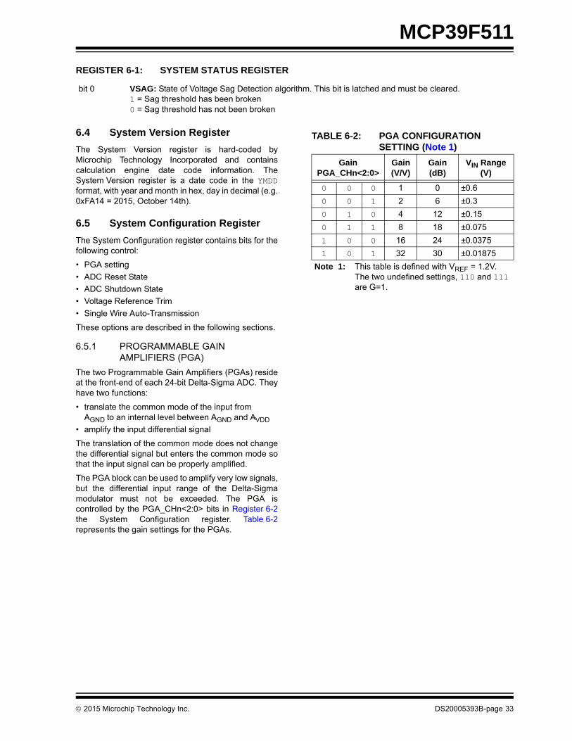
6.4 System Version Register
The System Version register is hard-coded byMicrochip Technology Incorporated and containscalculation engine date code information. TheSystem Version register is a date code in the YMDDformat, with year and month in hex, day in decimal (e.g.0xFA14 = 2015, October 14th).
6.5 System Configuration Register
The System Configuration register contains bits for thefollowing control:
• PGA setting
• ADC Reset State
• ADC Shutdown State
• Voltage Reference Trim
• Single Wire Auto-Transmission
These options are described in the following sections.
6.5.1 PROGRAMMABLE GAIN AMPLIFIERS (PGA)
The two Programmable Gain Amplifiers (PGAs) resideat the front-end of each 24-bit Delta-Sigma ADC. Theyhave two functions:
• translate the common mode of the input from AGND to an internal level between AGND and AVDD
• amplify the input differential signal
The translation of the common mode does not changethe differential signal but enters the common mode sothat the input signal can be properly amplified.
The PGA block can be used to amplify very low signals,but the differential input range of the Delta-Sigmamodulator must not be exceeded. The PGA iscontrolled by the PGA_CHn<2:0> bits in Register 6-2the System Configuration register. Table 6-2represents the gain settings for the PGAs.
bit 0 VSAG: State of Voltage Sag Detection algorithm. This bit is latched and must be cleared.1 = Sag threshold has been broken0 = Sag threshold has not been broken
REGISTER 6-1: SYSTEM STATUS REGISTER
TABLE 6-2: PGA CONFIGURATION SETTING (Note 1)
Gain PGA_CHn<2:0>
Gain(V/V)
Gain(dB)
VIN Range (V)
0 0 0 1 0 ±0.6
0 0 1 2 6 ±0.3
0 1 0 4 12 ±0.15
0 1 1 8 18 ±0.075
1 0 0 16 24 ±0.0375
1 0 1 32 30 ±0.01875
Note 1: This table is defined with VREF = 1.2V. The two undefined settings, 110 and 111 are G=1.
MCP39F511
DS20005393B-page 34 2015 Microchip Technology Inc.
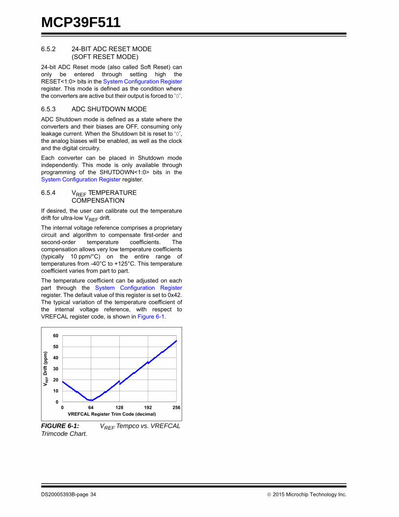
6.5.2 24-BIT ADC RESET MODE (SOFT RESET MODE)
24-bit ADC Reset mode (also called Soft Reset) canonly be entered through setting high theRESET<1:0> bits in the System Configuration Registerregister. This mode is defined as the condition wherethe converters are active but their output is forced to ‘0’.
6.5.3 ADC SHUTDOWN MODE
ADC Shutdown mode is defined as a state where theconverters and their biases are OFF, consuming onlyleakage current. When the Shutdown bit is reset to ‘0’,the analog biases will be enabled, as well as the clockand the digital circuitry.
Each converter can be placed in Shutdown modeindependently. This mode is only available throughprogramming of the SHUTDOWN<1:0> bits in theSystem Configuration Register register.
6.5.4 VREF TEMPERATURE COMPENSATION
If desired, the user can calibrate out the temperaturedrift for ultra-low VREF drift.
The internal voltage reference comprises a proprietarycircuit and algorithm to compensate first-order andsecond-order temperature coefficients. Thecompensation allows very low temperature coefficients(typically 10 ppm/°C) on the entire range oftemperatures from -40°C to +125°C. This temperaturecoefficient varies from part to part.
The temperature coefficient can be adjusted on eachpart through the System Configuration Registerregister. The default value of this register is set to 0x42.The typical variation of the temperature coefficient ofthe internal voltage reference, with respect toVREFCAL register code, is shown in Figure 6-1.
FIGURE 6-1: VREF Tempco vs. VREFCAL Trimcode Chart.
0
10
20
30
40
50
60
0 64 128 192 256
V REF
Drif
t (pp
m)
VREFCAL Register Trim Code (decimal)
2015 Microchip Technology Inc. DS20005393B-page 35
MCP39F511
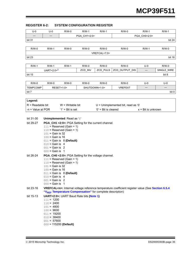
REGISTER 6-2: SYSTEM CONFIGURATION REGISTER
U-0 U-0 R/W-0 R/W-1 R/W-1 R/W-0 R/W-1 R/W-1
— — PGA_CH1<2:0> PGA_CH0<2:0>
bit 31 bit 24
R/W-0 R/W-1 R/W-0 R/W-0 R/W-0 R/W-0 R/W-1 R/W-0
VREFCAL<7:0>
bit 23 bit 16
R/W-1 R/W-1 R/W-1 R/W-0 R/W-0 R/W-0 U-0 R/W-0
UART<2:0>1 ZCD_INV ZCD_PULS ZCD_OUTPUT_DIS — SINGLE_WIRE
bit 15 bit 8
R/W-0 R/W-0 R/W-0 R/W-0 R/W-0 R/W-0 U-0 U-0
TEMPCOMP RESET<1:0> SHUTDOWN<1:0> VREFEXT — —
bit 7 bit 0
Legend:
R = Readable bit W = Writable bit U = Unimplemented bit, read as ‘0’
-n = Value at POR ‘1’ = Bit is set ‘0’ = Bit is cleared x = Bit is unknown
bit 31-30 Unimplemented: Read as ‘0’
bit 29-27 PGA_CH1 <2:0>: PGA Setting for the current channel.111 = Reserved (Gain = 1)110 = Reserved (Gain = 1)101 = Gain is 32100 = Gain is 16011 = Gain is 8 (Default)010 = Gain is 4001 = Gain is 2000 = Gain is 1
bit 26-24 PGA_CH0 <2:0>: PGA Setting for the voltage channel.111 = Reserved (Gain = 1)110 = Reserved (Gain = 1)101 = Gain is 32100 = Gain is 16011 = Gain is 8 (Default)010 = Gain is 4001 = Gain is 2000 = Gain is 1
bit 23-16 VREFCAL<n>: Internal voltage reference temperature coefficient register value (See Section 6.5.4 “VREF Temperature Compensation” for complete description)
bit 15-13 UART<2:0>: UART Baud Rate bits (Note 1)111 = 1200110 = 2400 101 = 4800100 = 9600011 = 19200010 = 38400001 = 57600000 = 115200 (Default)
MCP39F511
DS20005393B-page 36 2015 Microchip Technology Inc.
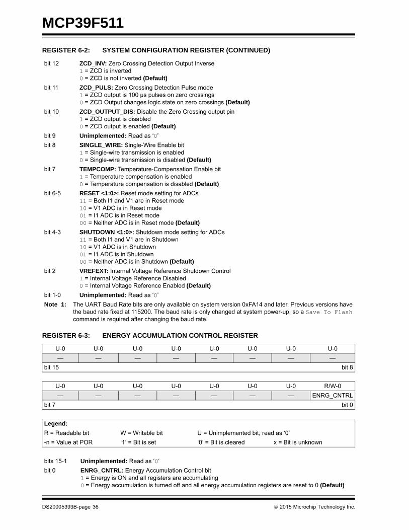
bit 12 ZCD_INV: Zero Crossing Detection Output Inverse1 = ZCD is inverted0 = ZCD is not inverted (Default)
bit 11 ZCD_PULS: Zero Crossing Detection Pulse mode1 = ZCD output is 100 µs pulses on zero crossings0 = ZCD Output changes logic state on zero crossings (Default)
bit 10 ZCD_OUTPUT_DIS: Disable the Zero Crossing output pin1 = ZCD output is disabled0 = ZCD output is enabled (Default)
bit 9 Unimplemented: Read as ‘0’
bit 8 SINGLE_WIRE: Single-Wire Enable bit1 = Single-wire transmission is enabled0 = Single-wire transmission is disabled (Default)
bit 7 TEMPCOMP: Temperature-Compensation Enable bit1 = Temperature compensation is enabled0 = Temperature compensation is disabled (Default)
bit 6-5 RESET <1:0>: Reset mode setting for ADCs11 = Both I1 and V1 are in Reset mode10 = V1 ADC is in Reset mode01 = I1 ADC is in Reset mode00 = Neither ADC is in Reset mode (Default)
bit 4-3 SHUTDOWN <1:0>: Shutdown mode setting for ADCs11 = Both I1 and V1 are in Shutdown10 = V1 ADC is in Shutdown01 = I1 ADC is in Shutdown00 = Neither ADC is in Shutdown (Default)
bit 2 VREFEXT: Internal Voltage Reference Shutdown Control1 = Internal Voltage Reference Disabled0 = Internal Voltage Reference Enabled (Default)
bit 1-0 Unimplemented: Read as ‘0’
Note 1: The UART Baud Rate bits are only available on system version 0xFA14 and later. Previous versions have the baud rate fixed at 115200. The baud rate is only changed at system power-up, so a Save To Flash command is required after changing the baud rate.
REGISTER 6-3: ENERGY ACCUMULATION CONTROL REGISTER
U-0 U-0 U-0 U-0 U-0 U-0 U-0 U-0
— — — — — — — —
bit 15 bit 8
U-0 U-0 U-0 U-0 U-0 U-0 U-0 R/W-0
— — — — — — — ENRG_CNTRL
bit 7 bit 0
Legend:
R = Readable bit W = Writable bit U = Unimplemented bit, read as ‘0’
-n = Value at POR ‘1’ = Bit is set ‘0’ = Bit is cleared x = Bit is unknown
bits 15-1 Unimplemented: Read as ‘0‘
bit 0 ENRG_CNTRL: Energy Accumulation Control bit1 = Energy is ON and all registers are accumulating0 = Energy accumulation is turned off and all energy accumulation registers are reset to 0 (Default)
REGISTER 6-2: SYSTEM CONFIGURATION REGISTER (CONTINUED)
2015 Microchip Technology Inc. DS20005393B-page 37
MCP39F511
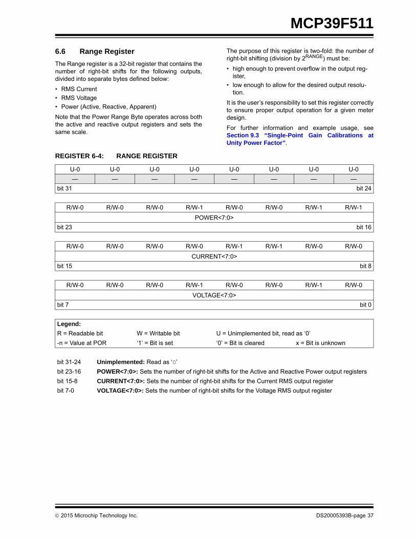
6.6 Range Register
The Range register is a 32-bit register that contains thenumber of right-bit shifts for the following outputs,divided into separate bytes defined below:
• RMS Current
• RMS Voltage
• Power (Active, Reactive, Apparent)
Note that the Power Range Byte operates across boththe active and reactive output registers and sets thesame scale.
The purpose of this register is two-fold: the number ofright-bit shifting (division by 2RANGE) must be:
• high enough to prevent overflow in the output reg-ister,
• low enough to allow for the desired output resolu-tion.
It is the user’s responsibility to set this register correctlyto ensure proper output operation for a given meterdesign.
For further information and example usage, seeSection 9.3 “Single-Point Gain Calibrations atUnity Power Factor”.
.
REGISTER 6-4: RANGE REGISTER
U-0 U-0 U-0 U-0 U-0 U-0 U-0 U-0
— — — — — — — —
bit 31 bit 24
R/W-0 R/W-0 R/W-0 R/W-1 R/W-0 R/W-0 R/W-1 R/W-1
POWER<7:0>
bit 23 bit 16
R/W-0 R/W-0 R/W-0 R/W-0 R/W-1 R/W-1 R/W-0 R/W-0
CURRENT<7:0>
bit 15 bit 8
R/W-0 R/W-0 R/W-0 R/W-1 R/W-0 R/W-0 R/W-1 R/W-0
VOLTAGE<7:0>
bit 7 bit 0
Legend:
R = Readable bit W = Writable bit U = Unimplemented bit, read as ‘0’
-n = Value at POR ‘1’ = Bit is set ‘0’ = Bit is cleared x = Bit is unknown
bit 31-24 Unimplemented: Read as ‘0’
bit 23-16 POWER<7:0>: Sets the number of right-bit shifts for the Active and Reactive Power output registers
bit 15-8 CURRENT<7:0>: Sets the number of right-bit shifts for the Current RMS output register
bit 7-0 VOLTAGE<7:0>: Sets the number of right-bit shifts for the Voltage RMS output register

MCP39F511
DS20005393B-page 38 2015 Microchip Technology Inc.
NOTES:
2015 Microchip Technology Inc. DS20005393B-page 39
MCP39F511
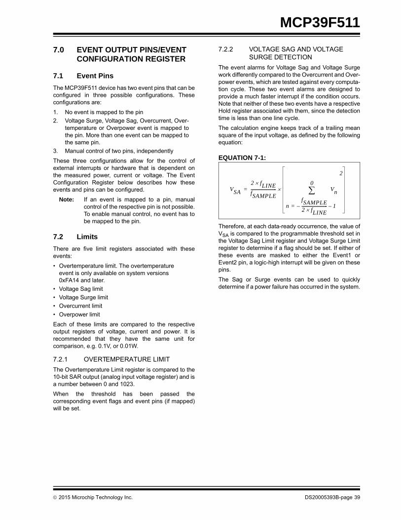
7.0 EVENT OUTPUT PINS/EVENT CONFIGURATION REGISTER
7.1 Event Pins
The MCP39F511 device has two event pins that can beconfigured in three possible configurations. Theseconfigurations are:
1. No event is mapped to the pin
2. Voltage Surge, Voltage Sag, Overcurrent, Over-temperature or Overpower event is mapped tothe pin. More than one event can be mapped tothe same pin.
3. Manual control of two pins, independently
These three configurations allow for the control ofexternal interrupts or hardware that is dependent onthe measured power, current or voltage. The EventConfiguration Register below describes how theseevents and pins can be configured.
Note: If an event is mapped to a pin, manualcontrol of the respective pin is not possible.To enable manual control, no event has tobe mapped to the pin.
7.2 Limits
There are five limit registers associated with theseevents:
• Overtemperature limit. The overtemperature event is only available on system versions 0xFA14 and later.
• Voltage Sag limit
• Voltage Surge limit
• Overcurrent limit
• Overpower limit
Each of these limits are compared to the respectiveoutput registers of voltage, current and power. It isrecommended that they have the same unit forcomparison, e.g. 0.1V, or 0.01W.
7.2.1 OVERTEMPERATURE LIMIT
The Overtemperature Limit register is compared to the10-bit SAR output (analog input voltage register) and isa number between 0 and 1023.
When the threshold has been passed thecorresponding event flags and event pins (if mapped)will be set.
7.2.2 VOLTAGE SAG AND VOLTAGE SURGE DETECTION
The event alarms for Voltage Sag and Voltage Surgework differently compared to the Overcurrent and Over-power events, which are tested against every computa-tion cycle. These two event alarms are designed toprovide a much faster interrupt if the condition occurs.Note that neither of these two events have a respectiveHold register associated with them, since the detectiontime is less than one line cycle.
The calculation engine keeps track of a trailing meansquare of the input voltage, as defined by the followingequation:
EQUATION 7-1:
Therefore, at each data-ready occurrence, the value ofVSA is compared to the programmable threshold set inthe Voltage Sag Limit register and Voltage Surge Limitregister to determine if a flag should be set. If either ofthese events are masked to either the Event1 orEvent2 pin, a logic-high interrupt will be given on thesepins.
The Sag or Surge events can be used to quicklydetermine if a power failure has occurred in the system.
VSA
2 f LINEfSAMPLE-------------------------- Vn
nfSAMPLE2 fLINE--------------------------– 1–=
0
2
=
MCP39F511
DS20005393B-page 40 2015 Microchip Technology Inc.
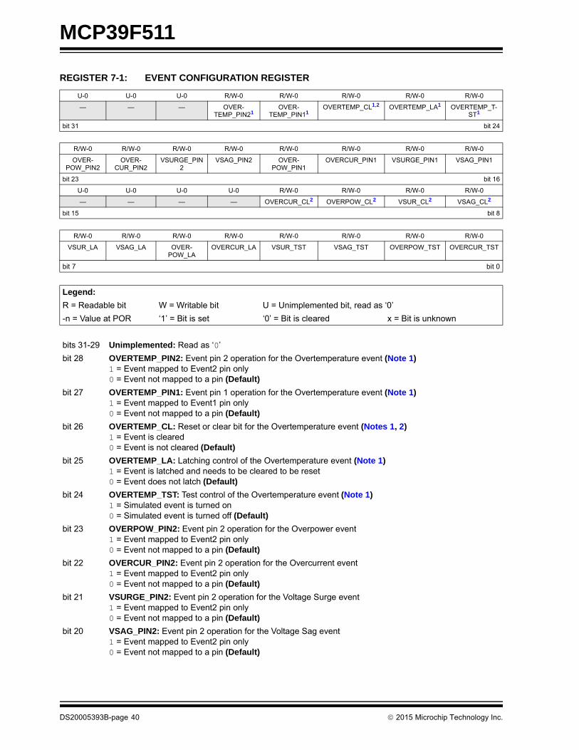
REGISTER 7-1: EVENT CONFIGURATION REGISTER
U-0 U-0 U-0 R/W-0 R/W-0 R/W-0 R/W-0 R/W-0
— — — OVER-TEMP_PIN21
OVER-TEMP_PIN11
OVERTEMP_CL1,2 OVERTEMP_LA1 OVERTEMP_T-ST1
bit 31 bit 24
R/W-0 R/W-0 R/W-0 R/W-0 R/W-0 R/W-0 R/W-0 R/W-0
OVER-POW_PIN2
OVER-CUR_PIN2
VSURGE_PIN2
VSAG_PIN2 OVER-POW_PIN1
OVERCUR_PIN1 VSURGE_PIN1 VSAG_PIN1
bit 23 bit 16
U-0 U-0 U-0 U-0 R/W-0 R/W-0 R/W-0 R/W-0
— — — — OVERCUR_CL2 OVERPOW_CL2 VSUR_CL2 VSAG_CL2
bit 15 bit 8
R/W-0 R/W-0 R/W-0 R/W-0 R/W-0 R/W-0 R/W-0 R/W-0
VSUR_LA VSAG_LA OVER-POW_LA
OVERCUR_LA VSUR_TST VSAG_TST OVERPOW_TST OVERCUR_TST
bit 7 bit 0
Legend:
R = Readable bit W = Writable bit U = Unimplemented bit, read as ‘0’
-n = Value at POR ‘1’ = Bit is set ‘0’ = Bit is cleared x = Bit is unknown
bits 31-29 Unimplemented: Read as ‘0’
bit 28 OVERTEMP_PIN2: Event pin 2 operation for the Overtemperature event (Note 1)1 = Event mapped to Event2 pin only0 = Event not mapped to a pin (Default)
bit 27 OVERTEMP_PIN1: Event pin 1 operation for the Overtemperature event (Note 1)1 = Event mapped to Event1 pin only0 = Event not mapped to a pin (Default)
bit 26 OVERTEMP_CL: Reset or clear bit for the Overtemperature event (Notes 1, 2)1 = Event is cleared0 = Event is not cleared (Default)
bit 25 OVERTEMP_LA: Latching control of the Overtemperature event (Note 1)1 = Event is latched and needs to be cleared to be reset0 = Event does not latch (Default)
bit 24 OVERTEMP_TST: Test control of the Overtemperature event (Note 1)1 = Simulated event is turned on0 = Simulated event is turned off (Default)
bit 23 OVERPOW_PIN2: Event pin 2 operation for the Overpower event1 = Event mapped to Event2 pin only0 = Event not mapped to a pin (Default)
bit 22 OVERCUR_PIN2: Event pin 2 operation for the Overcurrent event1 = Event mapped to Event2 pin only0 = Event not mapped to a pin (Default)
bit 21 VSURGE_PIN2: Event pin 2 operation for the Voltage Surge event1 = Event mapped to Event2 pin only0 = Event not mapped to a pin (Default)
bit 20 VSAG_PIN2: Event pin 2 operation for the Voltage Sag event1 = Event mapped to Event2 pin only0 = Event not mapped to a pin (Default)
2015 Microchip Technology Inc. DS20005393B-page 41
MCP39F511
bit 19 OVERPOW_PIN1: Event pin 1 operation for the Overpower event1 = Event mapped to Event1 pin only0 = Event not mapped to a pin (Default)
bit 18 OVERCUR_PIN1: Event pin 1 operation for the Overcurrent event1 = Event mapped to Event1 pin only0 = Event not mapped to a pin (Default)
bit 17 VSURGE_PIN1: Event pin 1 operation for the Voltage Surge event1 = Event mapped to Event1 pin only0 = Event not mapped to a pin (Default)
bit 16 VSAG_PIN1: Event pin 1 operation for the Voltage Sag event1 = Event mapped to Event1 pin only0 = Event not mapped to a pin (Default)
bits 15-12 Unimplemented: Read as ‘0’
bit 11 OVERCUR_CL: Reset or clear bit for the Overcurrent event (Note 2)1 = Event is cleared0 = Event is not cleared (Default)
bit 10 OVERPOW_CL: Reset or clear bit for the Overpower event (Note 2)1 = Event is cleared0 = Event is not cleared (Default)
bit 9 VSUR_CL: Reset or clear bit for the Voltage Surge event (Note 2)1 = Event is cleared0 = Event is not cleared (Default)
bit 8 VSAG_CL: Reset or clear bit for the Voltage Sag event (Note 2)1 = Event is cleared0 = Event is not cleared (Default)
bit 7 VSUR_LA: Latching control of the Voltage Surge event1 = Event is latched and needs to be cleared0 = Event does not latch (Default)
bit 6 VSAG_LA: Latching control of the Voltage Sag event1 = Event is latched and needs to be cleared0 = Event does not latch (Default)
bit 5 OVERPOW_LA: Latching control of the Overpower event1 = Event is latched and needs to be cleared0 = Event does not latch (Default)
bit 4 OVERCUR_LA: Latching control of the Overcurrent event1 = Event is latched and needs to be cleared0 = Event does not latch (Default)
bit 3 VSUR_TST: Test control of the Voltage Surge event1 = Simulated event is turned on0 = Simulated event is turned off (Default)
bit 2 VSAG_TST: Test control of the Voltage Sag event1 = Simulated event is turned on0 = Simulated event is turned off (Default)
bit 1 OVERPOW_TST: Test control of the Overpower event1 = Simulated event is turned on0 = Simulated event is turned off (Default)
bit 0 OVERCUR_TST: Test control of the Overcurrent event1 = Simulated event is turned on0 = Simulated event is turned off (Default)
Note 1: The Overtemperature event bits (28-24) are only available on system versions 0xFA14 and later.
2: Writing a 1 to the Clear bit clears the event, either real or simulated through test bits, and then returns to a state of 0.
REGISTER 7-1: EVENT CONFIGURATION REGISTER (CONTINUED)

MCP39F511
DS20005393B-page 42 2015 Microchip Technology Inc.
NOTES:
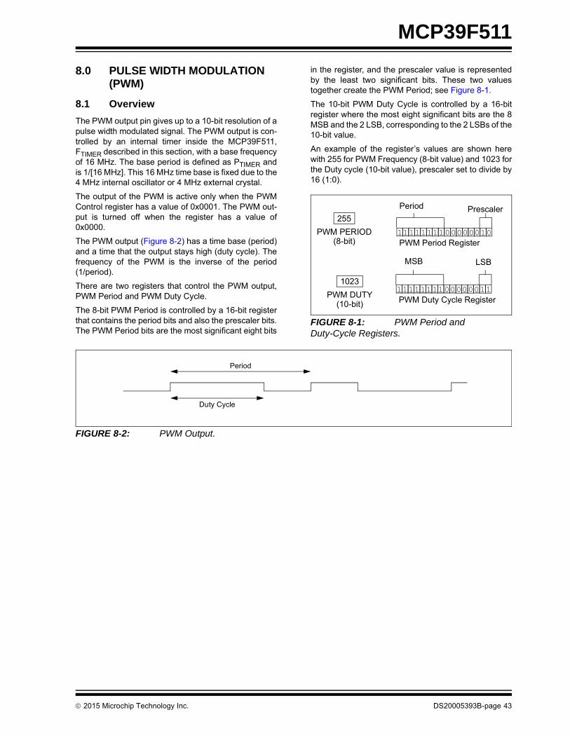
2015 Microchip Technology Inc. DS20005393B-page 43
MCP39F511
8.0 PULSE WIDTH MODULATION (PWM)
8.1 Overview
The PWM output pin gives up to a 10-bit resolution of apulse width modulated signal. The PWM output is con-trolled by an internal timer inside the MCP39F511,FTIMER described in this section, with a base frequencyof 16 MHz. The base period is defined as PTIMER andis 1/[16 MHz]. This 16 MHz time base is fixed due to the4 MHz internal oscillator or 4 MHz external crystal.
The output of the PWM is active only when the PWMControl register has a value of 0x0001. The PWM out-put is turned off when the register has a value of0x0000.
The PWM output (Figure 8-2) has a time base (period)and a time that the output stays high (duty cycle). Thefrequency of the PWM is the inverse of the period(1/period).
There are two registers that control the PWM output,PWM Period and PWM Duty Cycle.
The 8-bit PWM Period is controlled by a 16-bit registerthat contains the period bits and also the prescaler bits.The PWM Period bits are the most significant eight bits
in the register, and the prescaler value is representedby the least two significant bits. These two valuestogether create the PWM Period; see Figure 8-1.
The 10-bit PWM Duty Cycle is controlled by a 16-bitregister where the most eight significant bits are the 8MSB and the 2 LSB, corresponding to the 2 LSBs of the10-bit value.
An example of the register’s values are shown herewith 255 for PWM Frequency (8-bit value) and 1023 forthe Duty cycle (10-bit value), prescaler set to divide by16 (1:0).
FIGURE 8-1: PWM Period and Duty-Cycle Registers.
FIGURE 8-2: PWM Output.
PrescalerPeriod
11111111 00100000PWM Period Register
LSBMSB
11111111 00110000PWM Duty Cycle Register
255
1023
PWM PERIOD(8-bit)
PWM DUTY(10-bit)
Period
Duty Cycle
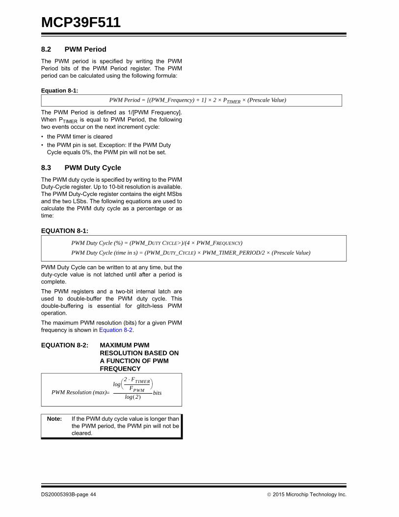
MCP39F511
DS20005393B-page 44 2015 Microchip Technology Inc.
8.2 PWM Period
The PWM period is specified by writing the PWMPeriod bits of the PWM Period register. The PWMperiod can be calculated using the following formula:
Equation 8-1:
The PWM Period is defined as 1/[PWM Frequency].When PTIMER is equal to PWM Period, the followingtwo events occur on the next increment cycle:
• the PWM timer is cleared
• the PWM pin is set. Exception: If the PWM Duty Cycle equals 0%, the PWM pin will not be set.
8.3 PWM Duty Cycle
The PWM duty cycle is specified by writing to the PWMDuty-Cycle register. Up to 10-bit resolution is available.The PWM Duty-Cycle register contains the eight MSbsand the two LSbs. The following equations are used tocalculate the PWM duty cycle as a percentage or astime:
EQUATION 8-1:
PWM Duty Cycle can be written to at any time, but theduty-cycle value is not latched until after a period iscomplete.
The PWM registers and a two-bit internal latch areused to double-buffer the PWM duty cycle. Thisdouble-buffering is essential for glitch-less PWMoperation.
The maximum PWM resolution (bits) for a given PWMfrequency is shown in Equation 8-2.
EQUATION 8-2: MAXIMUM PWM RESOLUTION BASED ON A FUNCTION OF PWM FREQUENCY
PWM Period = [(PWM_Frequency) + 1] × 2 × PTIMER × (Prescale Value)
PWM Duty Cycle (%) = (PWM_DUTY CYCLE>)/(4 × PWM_FREQUENCY)
PWM Duty Cycle (time in s) = (PWM_DUTY_CYCLE) × PWM_TIMER_PERIOD/2 × (Prescale Value)
Note: If the PWM duty cycle value is longer thanthe PWM period, the PWM pin will not becleared.
2 FTIMERFPWM
-------------------------- log
2 log----------------------------------------bits=PWM Resolution (max)
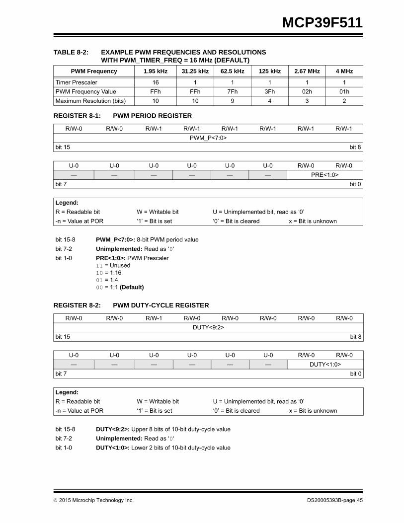
2015 Microchip Technology Inc. DS20005393B-page 45
MCP39F511
TABLE 8-2: EXAMPLE PWM FREQUENCIES AND RESOLUTIONS WITH PWM_TIMER_FREQ = 16 MHz (DEFAULT)
PWM Frequency 1.95 kHz 31.25 kHz 62.5 kHz 125 kHz 2.67 MHz 4 MHz
Timer Prescaler 16 1 1 1 1 1
PWM Frequency Value FFh FFh 7Fh 3Fh 02h 01h
Maximum Resolution (bits) 10 10 9 4 3 2
REGISTER 8-1: PWM PERIOD REGISTER
R/W-0 R/W-0 R/W-1 R/W-1 R/W-1 R/W-1 R/W-1 R/W-1
PWM_P<7:0>
bit 15 bit 8
U-0 U-0 U-0 U-0 U-0 U-0 R/W-0 R/W-0
— — — — — — PRE<1:0>
bit 7 bit 0
Legend:
R = Readable bit W = Writable bit U = Unimplemented bit, read as ‘0’
-n = Value at POR ‘1’ = Bit is set ‘0’ = Bit is cleared x = Bit is unknown
bit 15-8 PWM_P<7:0>: 8-bit PWM period value
bit 7-2 Unimplemented: Read as ‘0‘
bit 1-0 PRE<1:0>: PWM Prescaler11 = Unused10 = 1:1601 = 1:400 = 1:1 (Default)
REGISTER 8-2: PWM DUTY-CYCLE REGISTER
R/W-0 R/W-0 R/W-1 R/W-0 R/W-0 R/W-0 R/W-0 R/W-0
DUTY<9:2>
bit 15 bit 8
U-0 U-0 U-0 U-0 U-0 U-0 R/W-0 R/W-0
— — — — — — DUTY<1:0>
bit 7 bit 0
Legend:
R = Readable bit W = Writable bit U = Unimplemented bit, read as ‘0’
-n = Value at POR ‘1’ = Bit is set ‘0’ = Bit is cleared x = Bit is unknown
bit 15-8 DUTY<9:2>: Upper 8 bits of 10-bit duty-cycle value
bit 7-2 Unimplemented: Read as ‘0‘
bit 1-0 DUTY<1:0>: Lower 2 bits of 10-bit duty-cycle value
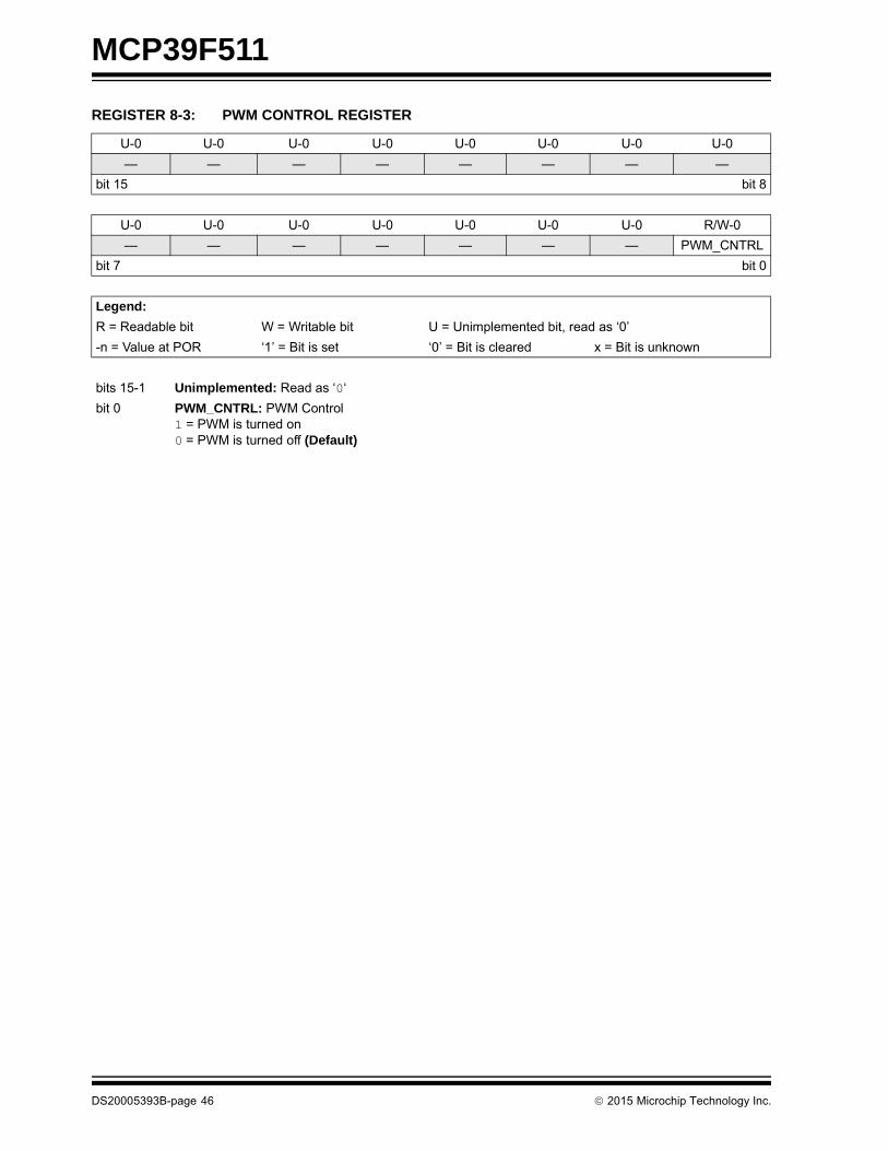
MCP39F511
DS20005393B-page 46 2015 Microchip Technology Inc.
REGISTER 8-3: PWM CONTROL REGISTER
U-0 U-0 U-0 U-0 U-0 U-0 U-0 U-0
— — — — — — — —
bit 15 bit 8
U-0 U-0 U-0 U-0 U-0 U-0 U-0 R/W-0
— — — — — — — PWM_CNTRL
bit 7 bit 0
Legend:
R = Readable bit W = Writable bit U = Unimplemented bit, read as ‘0’
-n = Value at POR ‘1’ = Bit is set ‘0’ = Bit is cleared x = Bit is unknown
bits 15-1 Unimplemented: Read as ‘0‘
bit 0 PWM_CNTRL: PWM Control1 = PWM is turned on0 = PWM is turned off (Default)
2015 Microchip Technology Inc. DS20005393B-page 47
MCP39F511
9.0 MCP39F511 CALIBRATION
9.1 Overview
Calibration compensates for ADC gain error,component tolerances and overall noise in the system.The device provides an on-chip calibration algorithmthat allows simple system calibration to be performedquickly. The excellent analog performance of theA/D converters on the MCP39F511 allows for asingle-point calibration and a single calibrationcommand to achieve accurate measurements.
Calibration can be done by either using the predefinedauto-calibration commands, or by writing directly to thecalibration registers. If additional calibration points arerequired (AC offset, Phase Compensation, DC offset),the corresponding calibration registers are available tothe user and will be described separately in thissection.
9.2 Calibration Order
The proper steps for calibration need to be maintained.
If the device has an external temperature sensorattached, temperature calibration should be done firstby reading the value from the Thermistor Voltageregister and copying the value by writing to the AmbientTemperature Reference Voltage register.
The single-point gain calibration at unity power factorshould be performed next.
If nonunity displacement power factor measurementsare a concern, then the next step should be Phasecalibration, followed by Reactive Power Gaincalibration.
Here is a summary on the order of calibration steps:
1. Transfer of the ambient temperature valueduring calibration to the Ambient TemperatureCalibration register for temperaturecompensation (optional)
2. Line Frequency Calibration
3. Gain Calibration at PF = 1
4. Phase Calibration at PF 1 (optional)
5. Reactive Gain Calibration at PF 1(optional)
Note: Only needed if temperature compensationis required. On system versions 0xFA14and later this register transfer is done auto-matically.
9.3 Single-Point Gain Calibrations at Unity Power Factor
When using the device in AC mode with the high-passfilters turned on, most offset errors are removed andonly a single-point gain calibration is required.
Setting the gain registers to properly produce thedesired outputs can be done manually by writing to theappropriate register. The alternative method is to usethe auto-calibration commands described in thissection.
9.3.1 USING THE AUTO-CALIBRATION GAIN COMMAND
By applying stable reference voltages and currents thatare equivalent to the values that reside in the targetCalibration Current, Calibration Voltage and CalibrationActive Power registers, the Auto-CalibrationGain command can then be issued to the device.
After a successful calibration (response = ACK), aSave Registers to Flash command can then beissued to save the calibration constants calculated bythe device.
The following registers are set when theAuto-Calibration Gain command is issued:
• Gain Current RMS
• Gain Voltage RMS
• Gain Active Power
When this command is issued, the MCP39F511attempts to match the expected values to the mea-sured values for all three output quantities by changingthe gain register based on the following formula:
EQUATION 9-1:
The same formula applies for Voltage RMS, CurrentRMS and Active power. Since the gain registers for allthree quantities are 16-bit numbers, the ratio of theexpected value to the measured value (which can bemodified by changing the Range register) and theprevious gain must be such that the equation yields avalid number. Here the limits are set to be from 25,000to 65,535. A new gain within this range for all threelimits will return an ACK for a successful calibration,otherwise the command returns a NAK for a failedcalibration attempt.
It is the user’s responsibility to ensure that the properrange settings, PGA settings and hardware designsettings are correct to allow for successful calibrationusing this command.
GAINNEW GAINOLDExpectedMeasured--------------------------=
MCP39F511
DS20005393B-page 48 2015 Microchip Technology Inc.
9.3.2 EXAMPLE OF RANGE SELECTION FOR VALID CALIBRATION
In this example, the user applies a calibration currentof 1A to an uncalibrated system. The indicated valuein the Current RMS register is 2300 with the system'sspecific shunt value, PGA gain, etc. The user expectsto see a value of 1000 in the Current RMS registerwhen 1A current is applied, meaning 1.000A with1 mA resolution. Other given values are:
• the existing value for Gain Current RMS is 33480
• the existing value for Range is 12
By using Equation 9-1, the calculation for GainNEWyields:
EQUATION 9-2:
When using the Auto-Calibration Gain com-mand, the result would be a failed calibration or a NAKreturned form the MCP39F511, because the resultingGainNEW is less than 25,000.
The solution is to use the Range register to bring themeasured value closer to the expected value, suchthat a new gain value can be calculated within thelimits specified above.
The Range register specifies the number of right-bitshifts (equivalent to divisions by 2) after themultiplication with the Gain Current RMS register.Refer to Section 5.0 “Calculation Engine (CE)Description” for information on the Range register.
Incrementing the Range register by 1 unit, an addi-tional right-bit shift or ÷2 is included in the calculation.Increasing the current range from 12 to 13 yields thenew measured Current RMS register value of 2300/2= 1150. The expected (1000) and measured (1150)are much closer now, so the expected new gainshould be within the limits:
EQUATION 9-3:
The resulting new gain is within the limits and thedevice successfully calibrates Current RMS andreturns an ACK.
Notice that the range can be set to 14 and the result-ing new gain will still be within limits(GainNEW = 58226). However, since this gain value isclose to the limit of the 16-bit Gain register, variationsfrom system to system (component tolerances, etc.)might create a scenario where the calibration is notsuccessful on some units and there would be a yield
issue. The best approach is to choose a range valuethat places the new gain in the middle of the bounds ofthe gain registers described above.
In a second example, when applying 1A, the userexpects an output of 1.0000A with 0.1 mA resolution.The example is starting with the same initial values:
EQUATION 9-4:
The GainNEW is much larger than the 16-bit limit of65535, so fewer right-bit shifts must be introduced toget the measured value closer to the expected value.The user needs to compute the number of bit shiftsthat will give a value lower than 65535. To estimatethis number:
EQUATION 9-5:
2.2 rounds to the closest integer value of 2. The rangevalue changes to 12 – 2 = 10; there are 2 less right-bitshifts.
The new measured value will be 2300 x 22 = 9200.
EQUATION 9-6:
The resulting new gain is within the limits and thedevice successfully calibrates Current RMS andreturns an ACK.
GAINNEW GAINOLDExpectedMeasured--------------------------- 33480
10002300------------ 14556===
14556 25 000
GAINNEW GAINOLDExpectedMeasured--------------------------- 33480
10001150------------ 29113===
25 000 29113 65535
GAINNEW GAINOLDExpectedMeasured--------------------------- 33480
100002300
--------------- 145565===
145565 65535
14556565535
------------------ 2.2=
GAINNEW GAINOLDExpectedMeasured--------------------------- 33480
100009200
--------------- 36391===
25 000 36391 65535
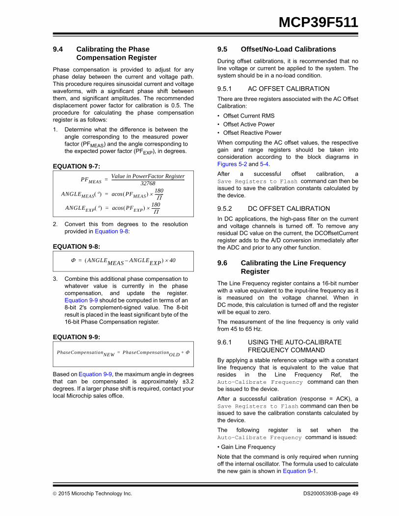
2015 Microchip Technology Inc. DS20005393B-page 49
MCP39F511
9.4 Calibrating the Phase Compensation Register
Phase compensation is provided to adjust for anyphase delay between the current and voltage path.This procedure requires sinusoidal current and voltagewaveforms, with a significant phase shift betweenthem, and significant amplitudes. The recommendeddisplacement power factor for calibration is 0.5. Theprocedure for calculating the phase compensationregister is as follows:
1. Determine what the difference is between theangle corresponding to the measured powerfactor (PFMEAS) and the angle corresponding tothe expected power factor (PFEXP), in degrees.
EQUATION 9-7:
2. Convert this from degrees to the resolutionprovided in Equation 9-8:
EQUATION 9-8:
3. Combine this additional phase compensation towhatever value is currently in the phasecompensation, and update the register.Equation 9-9 should be computed in terms of an8-bit 2's complement-signed value. The 8-bitresult is placed in the least significant byte of the16-bit Phase Compensation register.
EQUATION 9-9:
Based on Equation 9-9, the maximum angle in degreesthat can be compensated is approximately ±3.2degrees. If a larger phase shift is required, contact yourlocal Microchip sales office.
9.5 Offset/No-Load Calibrations
During offset calibrations, it is recommended that noline voltage or current be applied to the system. Thesystem should be in a no-load condition.
9.5.1 AC OFFSET CALIBRATION
There are three registers associated with the AC OffsetCalibration:
• Offset Current RMS
• Offset Active Power
• Offset Reactive Power
When computing the AC offset values, the respectivegain and range registers should be taken intoconsideration according to the block diagrams inFigures 5-2 and 5-4.
After a successful offset calibration, aSave Registers to Flash command can then beissued to save the calibration constants calculated bythe device.
9.5.2 DC OFFSET CALIBRATION
In DC applications, the high-pass filter on the currentand voltage channels is turned off. To remove anyresidual DC value on the current, the DCOffsetCurrentregister adds to the A/D conversion immediately afterthe ADC and prior to any other function.
9.6 Calibrating the Line Frequency Register
The Line Frequency register contains a 16-bit numberwith a value equivalent to the input-line frequency as itis measured on the voltage channel. When inDC mode, this calculation is turned off and the registerwill be equal to zero.
The measurement of the line frequency is only validfrom 45 to 65 Hz.
9.6.1 USING THE AUTO-CALIBRATE FREQUENCY COMMAND
By applying a stable reference voltage with a constantline frequency that is equivalent to the value thatresides in the Line Frequency Ref, theAuto-Calibrate Frequency command can thenbe issued to the device.
After a successful calibration (response = ACK), aSave Registers to Flash command can then beissued to save the calibration constants calculated bythe device.
The following register is set when theAuto-Calibrate Frequency command is issued:
• Gain Line Frequency
Note that the command is only required when runningoff the internal oscillator. The formula used to calculatethe new gain is shown in Equation 9-1.
PFMEASValue in PowerFactor Register
32768---------------------------------------------------------------------------=
ANGLEMEAS PFMEAS 180
---------acos=
ANGLEEXP PFEXP 180
---------acos=
ANGLEMEAS ANGLEEXP– 40=
PhaseCompensationNEW PhaseCompensationOLD +=
MCP39F511
DS20005393B-page 50 2015 Microchip Technology Inc.
9.7 Temperature Compensation
MCP39F511 measures the indication of thetemperature sensor and uses the value to compensatethe temperature variation of the shunt resistance andthe frequency of the internal RC oscillator.
The same formula applies for Line Frequency, CurrentRMS, Active Power and Reactive Power. Thetemperature compensation coefficient depends on the16-bit signed integer value of the correspondingcompensation register.
EQUATION 9-10:
At the calibration temperature, the effect of the com-pensation coefficients is minimal. The coefficients needto be tuned when the difference between the calibrationtemperature and the device temperature is significant.It is recommended to use the default values as startingpoints.
9.8 Retrieving Factory Default Calibration Values
After user calibration and a Save to Flashcommand has been issued, it is possible to retrieve thefactory default calibration values. This can be done bywriting 0xA5A5 to the calibration delimiter register,issuing a Save to Flash, and then resetting the part.This procedure will retrieve all factory-defaultcalibration values and will remain in this state untilcalibration has been performed again, and aSave to Flash command has been issued.
y x 1 c T TCAL– + =
Where:
x = Uncompensated Output (corresponding toLine Frequency, Current RMS, Active Powerand Reactive Power)
y = Compensated Output
c = Temperature Compensation Coefficient(depending on the shunt's TemperatureCoefficient of Resistance or on the internal RCoscillator temperature frequency drift). Thereare three registers one for Line Frequencycompensation, one for Current compensation,and one for power compensation (Active andReactive)
T = Thermistor Voltage (in 10-bit ADC units)
TCAL = Ambient Temperature Reference Voltage. Itshould be set at the beginning of thecalibration procedure, by reading thethermistor voltage and writing its value to theambient temperature reference voltageregister.
M = 26 (for Line Frequency compensation)
= 27 (for Current, Active Power and ReactivePower)
cTemperatureCompensation Register
2M
-----------------------------------------------------------------------------------------------=
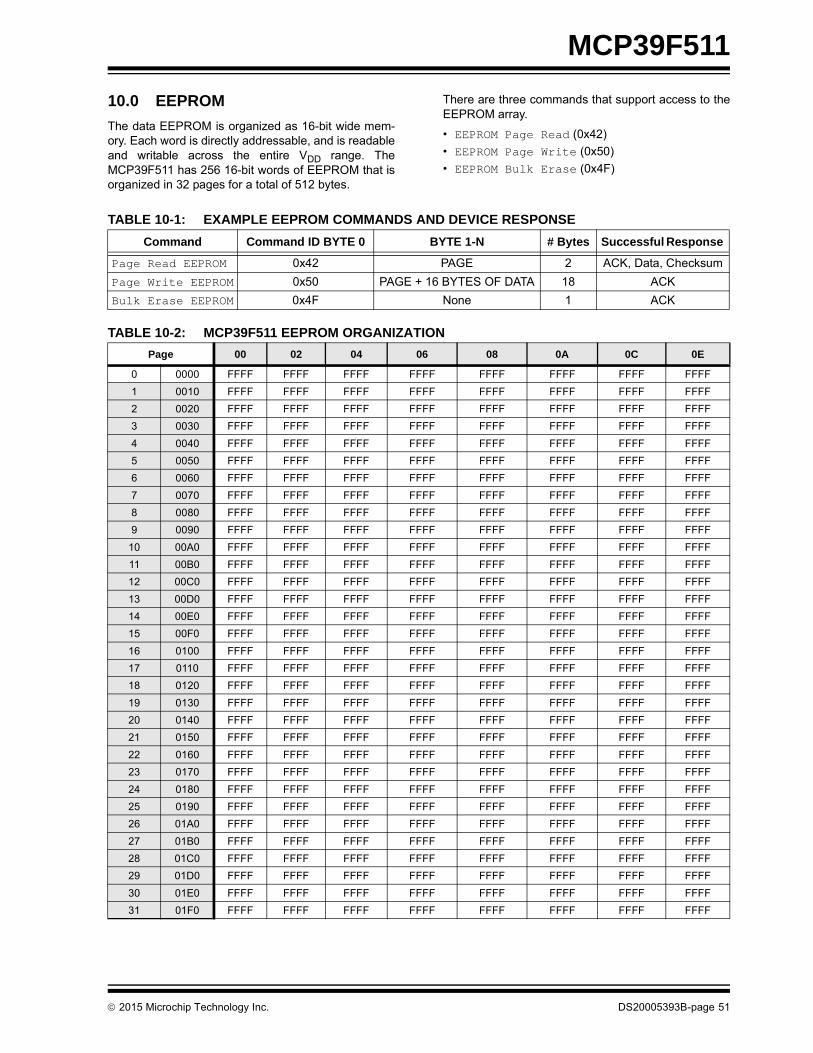
2015 Microchip Technology Inc. DS20005393B-page 51
MCP39F511
10.0 EEPROM
The data EEPROM is organized as 16-bit wide mem-ory. Each word is directly addressable, and is readableand writable across the entire VDD range. TheMCP39F511 has 256 16-bit words of EEPROM that isorganized in 32 pages for a total of 512 bytes.
There are three commands that support access to theEEPROM array.
• EEPROM Page Read (0x42)
• EEPROM Page Write (0x50)
• EEPROM Bulk Erase (0x4F)
TABLE 10-1: EXAMPLE EEPROM COMMANDS AND DEVICE RESPONSE
Command Command ID BYTE 0 BYTE 1-N # Bytes Successful Response
Page Read EEPROM 0x42 PAGE 2 ACK, Data, Checksum
Page Write EEPROM 0x50 PAGE + 16 BYTES OF DATA 18 ACK
Bulk Erase EEPROM 0x4F None 1 ACK
TABLE 10-2: MCP39F511 EEPROM ORGANIZATION
Page 00 02 04 06 08 0A 0C 0E
0 0000 FFFF FFFF FFFF FFFF FFFF FFFF FFFF FFFF
1 0010 FFFF FFFF FFFF FFFF FFFF FFFF FFFF FFFF
2 0020 FFFF FFFF FFFF FFFF FFFF FFFF FFFF FFFF
3 0030 FFFF FFFF FFFF FFFF FFFF FFFF FFFF FFFF
4 0040 FFFF FFFF FFFF FFFF FFFF FFFF FFFF FFFF
5 0050 FFFF FFFF FFFF FFFF FFFF FFFF FFFF FFFF
6 0060 FFFF FFFF FFFF FFFF FFFF FFFF FFFF FFFF
7 0070 FFFF FFFF FFFF FFFF FFFF FFFF FFFF FFFF
8 0080 FFFF FFFF FFFF FFFF FFFF FFFF FFFF FFFF
9 0090 FFFF FFFF FFFF FFFF FFFF FFFF FFFF FFFF
10 00A0 FFFF FFFF FFFF FFFF FFFF FFFF FFFF FFFF
11 00B0 FFFF FFFF FFFF FFFF FFFF FFFF FFFF FFFF
12 00C0 FFFF FFFF FFFF FFFF FFFF FFFF FFFF FFFF
13 00D0 FFFF FFFF FFFF FFFF FFFF FFFF FFFF FFFF
14 00E0 FFFF FFFF FFFF FFFF FFFF FFFF FFFF FFFF
15 00F0 FFFF FFFF FFFF FFFF FFFF FFFF FFFF FFFF
16 0100 FFFF FFFF FFFF FFFF FFFF FFFF FFFF FFFF
17 0110 FFFF FFFF FFFF FFFF FFFF FFFF FFFF FFFF
18 0120 FFFF FFFF FFFF FFFF FFFF FFFF FFFF FFFF
19 0130 FFFF FFFF FFFF FFFF FFFF FFFF FFFF FFFF
20 0140 FFFF FFFF FFFF FFFF FFFF FFFF FFFF FFFF
21 0150 FFFF FFFF FFFF FFFF FFFF FFFF FFFF FFFF
22 0160 FFFF FFFF FFFF FFFF FFFF FFFF FFFF FFFF
23 0170 FFFF FFFF FFFF FFFF FFFF FFFF FFFF FFFF
24 0180 FFFF FFFF FFFF FFFF FFFF FFFF FFFF FFFF
25 0190 FFFF FFFF FFFF FFFF FFFF FFFF FFFF FFFF
26 01A0 FFFF FFFF FFFF FFFF FFFF FFFF FFFF FFFF
27 01B0 FFFF FFFF FFFF FFFF FFFF FFFF FFFF FFFF
28 01C0 FFFF FFFF FFFF FFFF FFFF FFFF FFFF FFFF
29 01D0 FFFF FFFF FFFF FFFF FFFF FFFF FFFF FFFF
30 01E0 FFFF FFFF FFFF FFFF FFFF FFFF FFFF FFFF
31 01F0 FFFF FFFF FFFF FFFF FFFF FFFF FFFF FFFF

MCP39F511
DS20005393B-page 52 2015 Microchip Technology Inc.
NOTES:
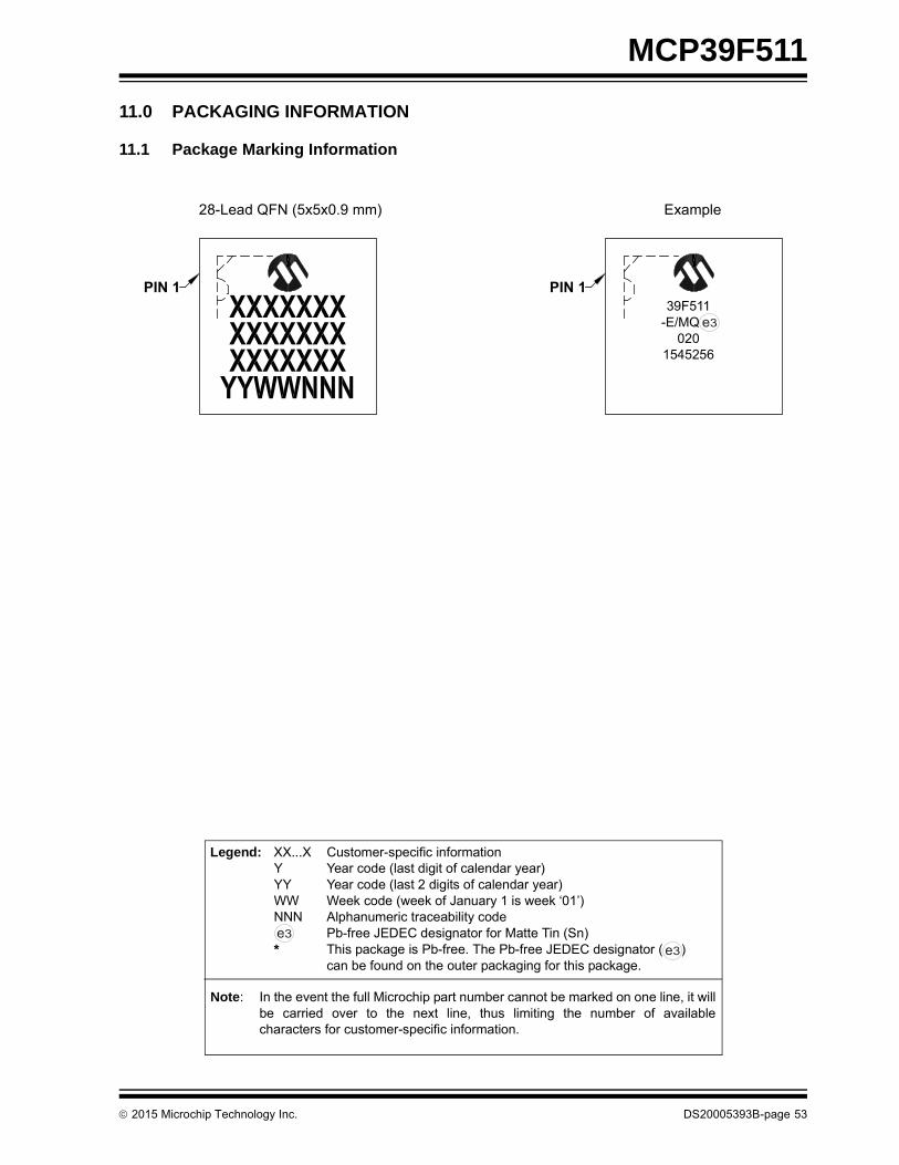
2015 Microchip Technology Inc. DS20005393B-page 53
MCP39F511
11.0 PACKAGING INFORMATION
11.1 Package Marking Information
Legend: XX...X Customer-specific informationY Year code (last digit of calendar year)YY Year code (last 2 digits of calendar year)WW Week code (week of January 1 is week ‘01’)NNN Alphanumeric traceability code Pb-free JEDEC designator for Matte Tin (Sn)* This package is Pb-free. The Pb-free JEDEC designator ( )
can be found on the outer packaging for this package.
Note: In the event the full Microchip part number cannot be marked on one line, it willbe carried over to the next line, thus limiting the number of availablecharacters for customer-specific information.
3e
3e
28-Lead QFN (5x5x0.9 mm) Example
PIN 1 PIN 139F511
-E/MQ ^^020
1545256
3e
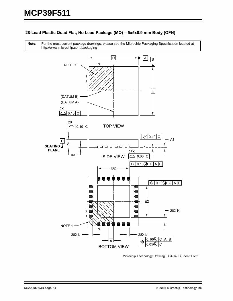
MCP39F511
DS20005393B-page 54 2015 Microchip Technology Inc.
BA
0.10 C
0.10 C
0.10 C A B0.05 C
(DATUM B)(DATUM A)
NOTE 1
2XTOP VIEW
SIDE VIEW
BOTTOM VIEW
For the most current package drawings, please see the Microchip Packaging Specification located athttp://www.microchip.com/packaging
Note:
NOTE 1
12
N
0.10 C A B
0.10 C A B
0.10 C
0.08 C
Microchip Technology Drawing C04-140C Sheet 1 of 2
28-Lead Plastic Quad Flat, No Lead Package (MQ) – 5x5x0.9 mm Body [QFN]
2X
28X
D
E
12
N
e
28X L
28X K
E2
D2
28X b
A3
AC
SEATINGPLANE
A1
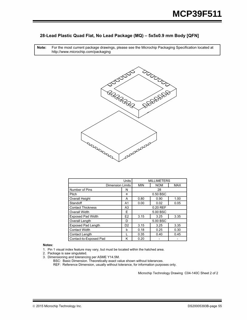
2015 Microchip Technology Inc. DS20005393B-page 55
MCP39F511
Microchip Technology Drawing C04-140C Sheet 2 of 2
For the most current package drawings, please see the Microchip Packaging Specification located athttp://www.microchip.com/packaging
Note:
28-Lead Plastic Quad Flat, No Lead Package (MQ) – 5x5x0.9 mm Body [QFN]
Dimension LimitsUnits
D
Overall Width
Overall LengthExposed Pad Length
Exposed Pad Width
Contact Thickness
D2
E2E
3.35
MILLIMETERS
0.20 REF
MIN
A3
MAX
5.00 BSC3.25
Contact LengthContact Width
Lb
0.450.30
Notes:1.
KContact-to-Exposed Pad 0.20
NOM
BSC: Basic Dimension. Theoretically exact value shown without tolerances.3.2.
REF: Reference Dimension, usually without tolerance, for information purposes only.
Standoff A1 0.02Overall Height A 0.90Pitch e 0.50 BSCNumber of Pins N 28
0.350.183.15
3.15
0.000.80
0.250.40
-
3.255.00 BSC
3.35
0.051.00
-
Pin 1 visual index feature may vary, but must be located within the hatched area.
Dimensioning and tolerancing per ASME Y14.5M.Package is saw singulated.
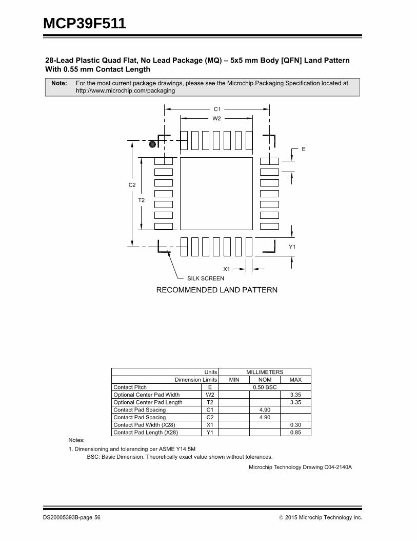
MCP39F511
DS20005393B-page 56 2015 Microchip Technology Inc.
28-Lead Plastic Quad Flat, No Lead Package (MQ) – 5x5 mm Body [QFN] Land PatternWith 0.55 mm Contact Length
Note: For the most current package drawings, please see the Microchip Packaging Specification located at http://www.microchip.com/packaging
Microchip Technology Drawing C04-2140A
2015 Microchip Technology Inc. DS20005393B-page 57
MCP39F511
APPENDIX A: REVISION HISTORY
Revision B (December 2015)
The following is the list of modifications:
• Document conforms to system version 0xFA14
• Overtemperature event added
• Selectable baud rate bits added to Register 6-2: System Configuration Register
• Various typographical edits
Revision A (March 2015)
• Original release of this document

MCP39F511
DS20005393B-page 58 2015 Microchip Technology Inc.
NOTES:
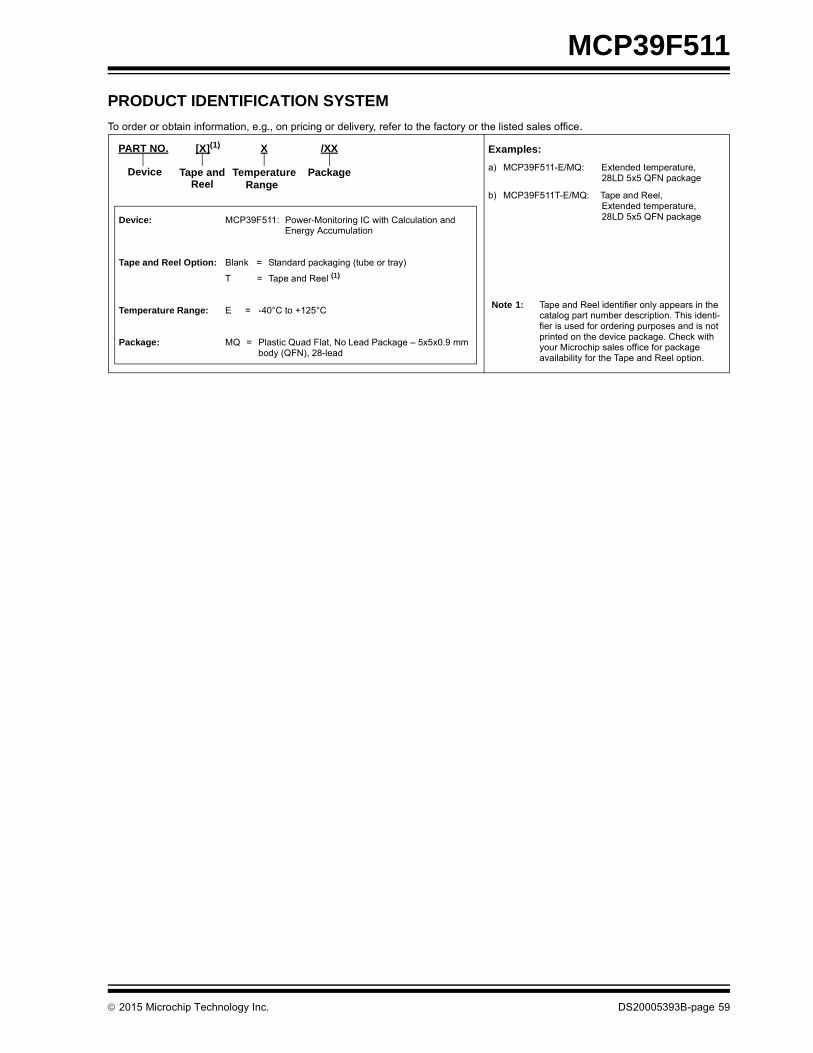
2015 Microchip Technology Inc. DS20005393B-page 59
MCP39F511
PRODUCT IDENTIFICATION SYSTEM
To order or obtain information, e.g., on pricing or delivery, refer to the factory or the listed sales office.
Device: MCP39F511: Power-Monitoring IC with Calculation and Energy Accumulation
Tape and Reel Option: Blank = Standard packaging (tube or tray)
T = Tape and Reel (1)
Temperature Range: E = -40°C to +125°C
Package: MQ = Plastic Quad Flat, No Lead Package – 5x5x0.9 mm body (QFN), 28-lead
Examples:
a) MCP39F511-E/MQ: Extended temperature,28LD 5x5 QFN package
b) MCP39F511T-E/MQ: Tape and Reel,Extended temperature,28LD 5x5 QFN package
PART NO. X
TemperatureRange
Device
/XX
Package
[X](1)
Tape andReel
Note 1: Tape and Reel identifier only appears in the catalog part number description. This identi-fier is used for ordering purposes and is not printed on the device package. Check with your Microchip sales office for package availability for the Tape and Reel option.

2015 Microchip Technology Inc. DS20005393B-page 60
MCP39F511
NOTES:
2015 Microchip Technology Inc. DS20005393B-page 61
Information contained in this publication regarding deviceapplications and the like is provided only for your convenienceand may be superseded by updates. It is your responsibility toensure that your application meets with your specifications.MICROCHIP MAKES NO REPRESENTATIONS ORWARRANTIES OF ANY KIND WHETHER EXPRESS ORIMPLIED, WRITTEN OR ORAL, STATUTORY OROTHERWISE, RELATED TO THE INFORMATION,INCLUDING BUT NOT LIMITED TO ITS CONDITION,QUALITY, PERFORMANCE, MERCHANTABILITY ORFITNESS FOR PURPOSE. Microchip disclaims all liabilityarising from this information and its use. Use of Microchipdevices in life support and/or safety applications is entirely atthe buyer’s risk, and the buyer agrees to defend, indemnify andhold harmless Microchip from any and all damages, claims,suits, or expenses resulting from such use. No licenses areconveyed, implicitly or otherwise, under any Microchipintellectual property rights unless otherwise stated.
Trademarks
The Microchip name and logo, the Microchip logo, dsPIC, FlashFlex, flexPWR, JukeBlox, KEELOQ, KEELOQ logo, Kleer, LANCheck, MediaLB, MOST, MOST logo, MPLAB, OptoLyzer, PIC, PICSTART, PIC32 logo, RightTouch, SpyNIC, SST, SST Logo, SuperFlash and UNI/O are registered trademarks of Microchip Technology Incorporated in the U.S.A. and other countries.
The Embedded Control Solutions Company and mTouch are registered trademarks of Microchip Technology Incorporated in the U.S.A.
Analog-for-the-Digital Age, BodyCom, chipKIT, chipKIT logo, CodeGuard, dsPICDEM, dsPICDEM.net, ECAN, In-Circuit Serial Programming, ICSP, Inter-Chip Connectivity, KleerNet, KleerNet logo, MiWi, motorBench, MPASM, MPF, MPLAB Certified logo, MPLIB, MPLINK, MultiTRAK, NetDetach, Omniscient Code Generation, PICDEM, PICDEM.net, PICkit, PICtail, RightTouch logo, REAL ICE, SQI, Serial Quad I/O, Total Endurance, TSHARC, USBCheck, VariSense, ViewSpan, WiperLock, Wireless DNA, and ZENA are trademarks of Microchip Technology Incorporated in the U.S.A. and other countries.
SQTP is a service mark of Microchip Technology Incorporated in the U.S.A.
Silicon Storage Technology is a registered trademark of Microchip Technology Inc. in other countries.
GestIC is a registered trademark of Microchip Technology Germany II GmbH & Co. KG, a subsidiary of Microchip Technology Inc., in other countries.
All other trademarks mentioned herein are property of their respective companies.
© 2015, Microchip Technology Incorporated, Printed in the U.S.A., All Rights Reserved.
ISBN: 978-1-5224-0068-4
Note the following details of the code protection feature on Microchip devices:
• Microchip products meet the specification contained in their particular Microchip Data Sheet.
• Microchip believes that its family of products is one of the most secure families of its kind on the market today, when used in the intended manner and under normal conditions.
• There are dishonest and possibly illegal methods used to breach the code protection feature. All of these methods, to our knowledge, require using the Microchip products in a manner outside the operating specifications contained in Microchip’s Data Sheets. Most likely, the person doing so is engaged in theft of intellectual property.
• Microchip is willing to work with the customer who is concerned about the integrity of their code.
• Neither Microchip nor any other semiconductor manufacturer can guarantee the security of their code. Code protection does not mean that we are guaranteeing the product as “unbreakable.”
Code protection is constantly evolving. We at Microchip are committed to continuously improving the code protection features of ourproducts. Attempts to break Microchip’s code protection feature may be a violation of the Digital Millennium Copyright Act. If such actsallow unauthorized access to your software or other copyrighted work, you may have a right to sue for relief under that Act.
Microchip received ISO/TS-16949:2009 certification for its worldwide headquarters, design and wafer fabrication facilities in Chandler and Tempe, Arizona; Gresham, Oregon and design centers in California and India. The Company’s quality system processes and procedures are for its PIC® MCUs and dsPIC® DSCs, KEELOQ® code hopping devices, Serial EEPROMs, microperipherals, nonvolatile memory and analog products. In addition, Microchip’s quality system for the design and manufacture of development systems is ISO 9001:2000 certified.
QUALITY MANAGEMENT SYSTEM CERTIFIED BY DNV
== ISO/TS 16949 ==

DS20005393B-page 62 2015 Microchip Technology Inc.
AMERICASCorporate Office2355 West Chandler Blvd.Chandler, AZ 85224-6199Tel: 480-792-7200 Fax: 480-792-7277Technical Support: http://www.microchip.com/supportWeb Address: www.microchip.com
AtlantaDuluth, GA Tel: 678-957-9614 Fax: 678-957-1455
Austin, TXTel: 512-257-3370
BostonWestborough, MA Tel: 774-760-0087 Fax: 774-760-0088
ChicagoItasca, IL Tel: 630-285-0071 Fax: 630-285-0075
ClevelandIndependence, OH Tel: 216-447-0464 Fax: 216-447-0643
DallasAddison, TX Tel: 972-818-7423 Fax: 972-818-2924
DetroitNovi, MI Tel: 248-848-4000
Houston, TX Tel: 281-894-5983
IndianapolisNoblesville, IN Tel: 317-773-8323Fax: 317-773-5453
Los AngelesMission Viejo, CA Tel: 949-462-9523 Fax: 949-462-9608
New York, NY Tel: 631-435-6000
San Jose, CA Tel: 408-735-9110
Canada - TorontoTel: 905-673-0699 Fax: 905-673-6509
ASIA/PACIFICAsia Pacific OfficeSuites 3707-14, 37th FloorTower 6, The GatewayHarbour City, Kowloon
Hong KongTel: 852-2943-5100Fax: 852-2401-3431
Australia - SydneyTel: 61-2-9868-6733Fax: 61-2-9868-6755
China - BeijingTel: 86-10-8569-7000 Fax: 86-10-8528-2104
China - ChengduTel: 86-28-8665-5511Fax: 86-28-8665-7889
China - ChongqingTel: 86-23-8980-9588Fax: 86-23-8980-9500
China - DongguanTel: 86-769-8702-9880
China - HangzhouTel: 86-571-8792-8115 Fax: 86-571-8792-8116
China - Hong Kong SARTel: 852-2943-5100 Fax: 852-2401-3431
China - NanjingTel: 86-25-8473-2460Fax: 86-25-8473-2470
China - QingdaoTel: 86-532-8502-7355Fax: 86-532-8502-7205
China - ShanghaiTel: 86-21-5407-5533 Fax: 86-21-5407-5066
China - ShenyangTel: 86-24-2334-2829Fax: 86-24-2334-2393
China - ShenzhenTel: 86-755-8864-2200 Fax: 86-755-8203-1760
China - WuhanTel: 86-27-5980-5300Fax: 86-27-5980-5118
China - XianTel: 86-29-8833-7252Fax: 86-29-8833-7256
ASIA/PACIFICChina - XiamenTel: 86-592-2388138 Fax: 86-592-2388130
China - ZhuhaiTel: 86-756-3210040 Fax: 86-756-3210049
India - BangaloreTel: 91-80-3090-4444 Fax: 91-80-3090-4123
India - New DelhiTel: 91-11-4160-8631Fax: 91-11-4160-8632
India - PuneTel: 91-20-3019-1500
Japan - OsakaTel: 81-6-6152-7160 Fax: 81-6-6152-9310
Japan - TokyoTel: 81-3-6880- 3770 Fax: 81-3-6880-3771
Korea - DaeguTel: 82-53-744-4301Fax: 82-53-744-4302
Korea - SeoulTel: 82-2-554-7200Fax: 82-2-558-5932 or 82-2-558-5934
Malaysia - Kuala LumpurTel: 60-3-6201-9857Fax: 60-3-6201-9859
Malaysia - PenangTel: 60-4-227-8870Fax: 60-4-227-4068
Philippines - ManilaTel: 63-2-634-9065Fax: 63-2-634-9069
SingaporeTel: 65-6334-8870Fax: 65-6334-8850
Taiwan - Hsin ChuTel: 886-3-5778-366Fax: 886-3-5770-955
Taiwan - KaohsiungTel: 886-7-213-7828
Taiwan - TaipeiTel: 886-2-2508-8600 Fax: 886-2-2508-0102
Thailand - BangkokTel: 66-2-694-1351Fax: 66-2-694-1350
EUROPEAustria - WelsTel: 43-7242-2244-39Fax: 43-7242-2244-393
Denmark - CopenhagenTel: 45-4450-2828 Fax: 45-4485-2829
France - ParisTel: 33-1-69-53-63-20 Fax: 33-1-69-30-90-79
Germany - DusseldorfTel: 49-2129-3766400
Germany - KarlsruheTel: 49-721-625370
Germany - MunichTel: 49-89-627-144-0 Fax: 49-89-627-144-44
Italy - Milan Tel: 39-0331-742611 Fax: 39-0331-466781
Italy - VeniceTel: 39-049-7625286
Netherlands - DrunenTel: 31-416-690399 Fax: 31-416-690340
Poland - WarsawTel: 48-22-3325737
Spain - MadridTel: 34-91-708-08-90Fax: 34-91-708-08-91
Sweden - StockholmTel: 46-8-5090-4654
UK - WokinghamTel: 44-118-921-5800Fax: 44-118-921-5820
Worldwide Sales and Service
07/14/15