Embed Size (px)
Citation preview

240
Opposite page:
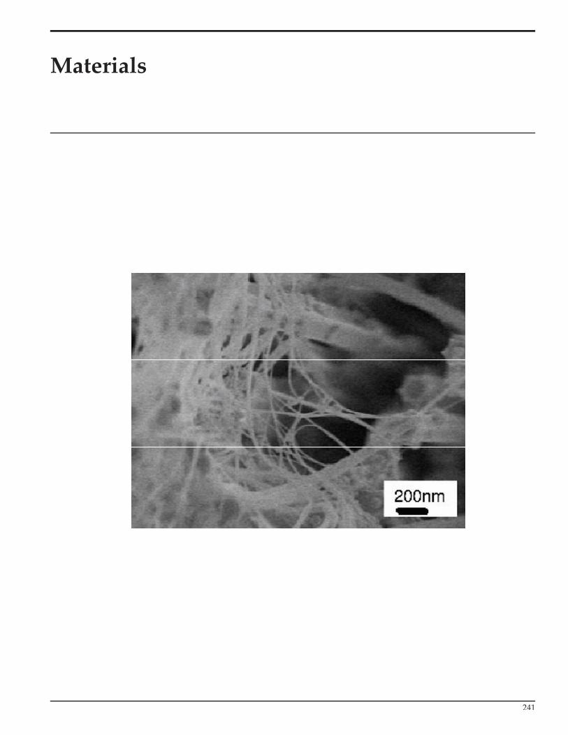
Gold nano-wires (~20nm) grown by halide reduction in nano-porous alumina template. Template chemically etched to expose nano-wires.
Courtesy of R. Krishnan, R. Tadepalli, and A. Giermann (C.V. Thompson in collaboration. with K. Nielsch, C.A. Ross, and H.I. Smith).
Sponsor:NSF and MARCO Focused Research Center on Interconnect (MARCO/DARPA)
241
Materials

242 Materials MTL Annual Report 2003
Materials
• Development of Processes and Technologies for Interconnects for 3D Integrated Circuits
• Interfacial Electromigration in Cu-Based On-Chip IC Interconnects
• Inelastic Deformation of Polycrystalline Films, Lines, and Dots
• Yellow-Green Emission for ETS-LEDs and Lasers Based on a Strained–InGaP Quantum Well Heterostructure Grown on a Transparent, Compositionally-Graded InAlGaP Buffer
• Ge Photodetectors for Si Microphotonics Circuits
• Epitaxial Growth of GaN on Silicon
• Integrated Materials Growth System
• Capillary Bonding of Nano-Structures
• Fabrication and Assembly of Metallic Nano-Wires, Rods, and Dots for Micro- and Nano-Systems
• Magnetic and Magnetooptical Films Made by Pulsed Laser Deposition
• Magnetic Thin Films
• Resonant Gas Sensors
• Stress Evolution During Reactive Film Formation
• Ferroelectrics for High Strain Actuation
• Stress Evolution During Volmer-Weber Growth of Thin Films
• Characterization of Electromigration-Induced Failure of Cu-Based ICInterconnect Trees for Circuit-Level Reliability Assessments

MTL Annual Report 2003 Materials 243
Development of Processes and Technologies for Interconnects for 3D Integrated Circuits
PersonnelR. Tadepalli and R. Krishnan (L. R. Reif, S. M. Spearing, and C. V. Thompson)
SponsorshipMARCO Focused Research Center on Interconnect (MARCO/DARPA)
The remarkable evolution of semiconductor technol-ogy has allowed production of integrated circuits with performance and functionality that have increased expo-nentially with time, while their cost has decreased expo-nentially with time. For this evolution to continue into the future, the critical dimensions in Ultra Large-Scale Integrated (ULSI) circuits must continue to shrink. As this happens, system performance will be increasingly dominated by interconnect delay. ICs laid out and fab-ricated in three dimensions, rather than the traditional two dimensions, can have reduced interconnect delay because of increased flexibility in system design and wiring placement and routing. The flexibility to place devices along the vertical dimension allows layout of circuits with higher device densities and reduced total interconnect lengths.
Wafer bonding is an attractive route to the fabrication of 3-D ICs. In this approach, previously processed device layers are bonded using metal-metal bonds that also serve as layer-to-layer interconnects. Evaluation of bond quality and reliability is critical to the implementation of wafer-bonded 3-D IC technology. Towards this end, we have developed techniques to measure the toughness of bonded copper interconnects. Bond toughness measure-ments were used to optimize the bonding process. High quality Cu-Cu bonds were fabricated at a low bonding temperature of 300 0C using a novel cleaning procedure.
A four-point bend technique has been employed to mea-sure the toughness of Cu-Cu bonds. Cu line structures that were patterned on oxidized silicon wafers were thermo-compression-bonded in the EV501 bond cham-ber and then tested for bond toughness. The bonding temperature, chamber ambient, and the pre-bonding clean procedures were varied to identify the optimized bonding route.
The results from mechanical testing are summarized in Figure 1. While toughness was found to increase mono-tonically with increasing bonding temperature, there is an obvious dependence of bond toughness on the cleaning methods and chamber ambient. A reducing gas (5% H2, 95% Ar) ambient improved the toughness and uniformity of Cu-Cu bonds. Best results were obtained by combining a glacial acetic acid pre-bond clean with a reducing gas chamber ambient, as is evident from the graph. A significant point of interest is that bonds creat-ed at 300 0C were comparable (17J/m2) to industry-stan-dard bonded SOI wafers (10J/m2) in terms of toughness values. This favorable comparison accentuates the supe-rior quality of bonds created at a low-k dielectric-com-patible temperature of 300 0C. Poor chamber vacuum conditions limit the ability to maintain ultra-clean Cu surfaces, thereby, limiting the quality of bonds. In-situ cleaning procedures would, however, provide a solution to this bottleneck.
Having developed a robust technique to evaluate bond quality, we are now fabricating test structures to study bond reliability. These electrical/mechanical structures will allow us to study statistical bond toughness varia-tions. Critical fabrication steps are: deep reactive ion etching to create through-wafer vias, electrodeposition for via filling, and CMP of Cu plated structures.
continued

244 Materials MTL Annual Report 2003
Fig. 1: Variation of bond toughness for wafers 0.4MPa thermo-com-pression bonded using 300nm-thick Cu films at different tempera-tures, after different surface preparations. Wafers bonded after an acetic acid pre-clean had higher bond toughness than bonded SOI wafers, even when bonded at temperatures below 300C. The point indicated by an ’*’ is a lower bound.
Interfacial Electromigration in Cu-Based On-Chip IC Interconnects
PersonnelZ. S. Choi, H. Verma, F. Wei, C. L. Gan, K. L. Pey, W. K. Choi, and R. Augur (C. V. Thompson)
SponsorshipIntel Corp., SRC, and SMA
Electromigration in polycrystalline Al-based interconnects is known to preferentially occur along grain boundaries. This leads to a very strong dependence of the reliability of Al-based interconnects on their grain structure, with interconnects with bamboo grain structures having reliabilities orders of magnitude higher than interconnects with polygranular grain structures. The factors relating grain structures to the reliability of Al-based interconnects, and relating processing conditions to grain structures, are relatively well understood.
With the move to lower resistance Cu-based intercon-nects, it has become clear that the role of grain struc-tures in determining reliability has become fundamen-tally different. Grain boundaries no longer provide preferred high-diffusivity paths for electromigration. Instead, the interfaces between Cu and the surround-ing diffusion barriers provide higher diffusivity paths. This is a consequence of the relatively high diffusivity at these interfaces in current Cu technology, rather than due to relatively low diffusivities in Cu grain boundar-ies. The barrier-Cu interfaces also appear to be sites for relatively easy stress-induced void formation, and for rapid electromigration-induced void growth. It appears that the interface between Cu and the interlevel diffu-sion barrier (typically SiN in current technology) is an especially easy site for void nucleation and growth, as well as a path for relatively rapid electromigration.
We have developed several test structures for experi-mental characterization of interfacial electromigration in Cu. One structure, a ‘drift structure’, consists of Cu lines patterned along the length of a continuous under-lying Ta line (See Figure 2). When current is passed through the Ta line, it shunts into the lower resistance Cu segments, when possible. At suffi ciently high cur-rents, this causes electromigration that leads the Cu to accumulate at the anode end of the segments and deplete at the cathode end, resulting in a ‘drift’ of the
continued
continued

MTL Annual Report 2003 Materials 245
Cu segments (See Figure 2b). Measuring the current density at which drift begins, as a function of segment length, as well as the rate of drift as a function of the current density, provides important information about interfacial electromigration. We are acquiring this infor-mation from drift structures that are not covered with a passivating layer, as well as structures with passivat-ing layers (e.g., SiN) (See Figure 2c), to investigate the effects of passivation layers on the stress required to initiate drift, as well as the drift velocity and its scaling with current density.
In a different set of experiments, we are using via-to-via test lines in a second layer of metallization, with con-necting lines and pads in the first layer of metallization, to characterize drift in fully-processed dual-damascene structures provided by Sematech International. In addi-tion to providing fully processed structures, Sematech has also provided samples that have been processed through chemical mechanical polishing of the second level of metallization. We have developed a process within MIT that allows us to complete the fabrication of test structures. This, in turn, allows us to investigate the effects of different interlevel diffusion barriers on top of the Cu test lines, as well as the effects of differ-ent surface treatments. Experiments of both types are underway.
In a related study we have characterized electromigration drift in fully processed via-to-via test structures of the type shown in Figure 3, as well as in similar structures in which the test line is in the first layer of metallization (M1). In both types of structures, we observed that in a significant fraction of the test population, the resistance of the lines increased steadily over time, prior to failure. We postulate that this gradual resistance increase results from void growth and that the rate of resistance increase correlates with the electromigration drift velocity (See Figure 4). The values of the electromigration drift velocities determined in M2 lines were similar to those
measured in M1 lines, though there was a broader range of variation in the former case. The larger variation is correlated with the larger range of void shapes and sizes in M2-type structures. Given that the stress for void nucleation should be the same, the observation that the rate of void growth is the same supports our earlier proposal that the asymmetry in reliability in these two different configurations is associated with differences in the void sizes required to cause failure.
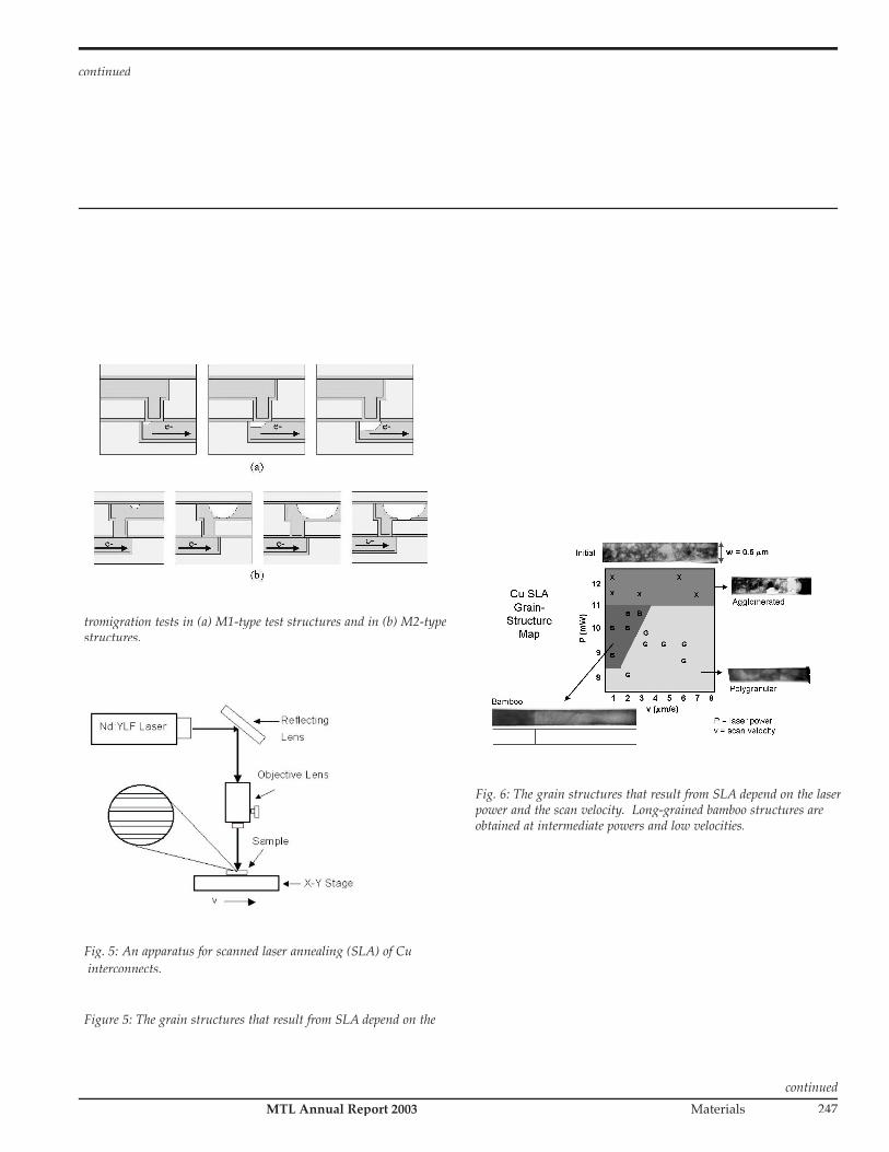
Using the interfacial electromigration test structures described above, we also plan to investigate the effects of grain structures and grain orientations on interfacial electromigration. To do this we will use Scanned Laser Annealing (SLA) of Cu lines to produce long-grained-bamboo or near-single-crystal Cu interconnects for elec-tromigration testing. This will allow characterization of electromigration and electromigration-induced void-ing for single-via and multi-via structures that contact single Cu grains or crystals.
In earlier work in our group, Scanned Laser Annealing (SLA) was developed as a means of modifying and con-trolling the grain structures of polycrystalline intercon-nects. In this technique, a laser spot is scanned along the length of an interconnect, to create a moving hot zone in which grain boundary mobilities are signifi-cantly increased over those of boundaries in unheated regions (See Figure 5). This leads to a grain growth in the hot zone, and as the zone is scanned, grain bound-ary motion is caused to occur preferentially and specifi-cally in the direction of zone motion. This technique can be used to produce bamboo grain structures in lines that would not develop bamboo grain structures in conventional anneals. Furthermore, the grain sizes obtained from scanned laser annealing can be signifi-cantly longer than those obtained from conventional annealing. Lines with bamboo grain sizes as long as 10µm were produced by scanned laser annealing of 0.5µm-wide Cu lines.
continued
continued

246 Materials MTL Annual Report 2003
Modeling of the SLA process suggests that still longer bamboo grains can be obtained under the proper condi-tions. In ongoing research, we will investigate this pos-sibility. We will also use SLA to produce large-grained structures in the dual-damascene drift structures described above. With Cu interconnects having 10µm-long grains or longer, contacted at either end with single vias, most vias will contact a single grain. By analyzing SLA grain structures before completing the process-ing of the electromigration test structures, we hope to assess the effect of grain crystallographic orientation on interfacial electromigration. The results will be used to develop models for interfacial electromigration in Cu interconnects that account for the effects of crystallo-graphic orientations.
Fig. 2: Drift test structure for characterization of interfacial electro-migration of Cu. (a) Cu segments are patterned on continuous Ta underlying lines. (b) Current shunts into the lower resistance Cu segment and causes it to drift. (c) Passivation will affect the rate and character of drift.
continued
continued
Fig. 3: A second structure for characterization of interfacial electro-migration of Cu. A via-to via metal 2 test line connected to larger metal 1 lines, connected to bond pads. (a) Conventional dual-dama-scene processing through CMP of metal 2 is carried out at Sematech. Metal 2 surface treatment and passivation, and the rest of the test structure processing, are carried out at MIT.
Fig. 4: Void growth causes a gradual resistance increase during elec-
MTL Annual Report 2003 Materials 247
tromigration tests in (a) M1-type test structures and in (b) M2-type structures.
Fig. 5: An apparatus for scanned laser annealing (SLA) of Cu interconnects.
Figure 5: The grain structures that result from SLA depend on the
continued
continued
Fig. 6: The grain structures that result from SLA depend on the laser power and the scan velocity. Long-grained bamboo structures are obtained at intermediate powers and low velocities.

248 Materials MTL Annual Report 2003
Inelastic Deformation of Polycrystalline Films, Lines, and Dots
PersonnelR. Bernstein (C. V. Thompson)
SponsorshipNSF and CMI
In earlier studies, we have characterized inelastic defor-mation of polycrystalline metallic films using in-situ Transmission Electron Microscopy (TEM), and ex-situ substrate curvature measurements during heating, cool-ing, and isothermal anneals. In-situ TEM studies were made possible through the use of micromachined silicon membranes. We have demonstrated that uncapped Ag and Cu fi lms undergo rapid diffusional creep at tem-peratures as low as 0.25Tm, where Tm is the melting temperature in degrees Kelvin. At these temperatures, creep rapidly decreases with decreasing fi lm thickness. This can lead to a decrease in the flow stress observed at room temperature as the film thickness is decreased. We have also demonstrated that dislocation-mediated plasticity dominates in capped films, or in uncapped films that are thicker or deformed at lower tempera-tures. We have shown that dislocation-mediated plas-ticity is thermally activated and controlled by pinning due to obstacles whose spacing is small compared to film thickness and grain size. This leads to the high flow stresses often observed in capped thin films. We have seen similar effects to those described above in Cu films patterned into lines through a damascene process. This work demonstrates that the inelastic properties of polycrystalline metallic films depend strongly on the film dimension, the surface condition of the film, and temperature.
We are currently investigating the use of micromachined cantilevers for isothermal studies of deformation of thin films and films patterned into dots. These cantilevers can be deflected at a set temperature, and the relaxation at that temperature can be studied. The deflection of the cantilevers can be measured with very high resolu-tion (of order nm) using an optical profilometer at fairly high sampling rates (up to once every five seconds).

MTL Annual Report 2003 Materials 249
Yellow-Green Emission for ETS-LEDs and Lasers Based on a Strained–InGaP Quantum Well Heterostructure Grown on a Transparent, Compositionally-Graded InAlGaP Buffer
PersonnelL. McGill and J. Wu (E.A. Fitzgerald)
SponsorshipNSF GOALI Program and ARO Program
Epitaxial-transparent-substrate light emitting diodes with a primary emission peak at 590nm and a secondary peak at 560nm have been fabricated in the indium alu-minum gallium phosphide (InAlGaP) system. The active layer consists of an undoped, compressively strained indium gallium phosphide (InGaP) quantum well on a transparent In0.22(Al0.2Ga0.8)0.78P/∇x[Inx(Al0.2Ga0.8)1-xP]/GaP virtual substrate. Light emitting diodes have been fabricated utilizing simple top and bottom con-tacts. The highest LED power of 0.18μW per facet at 20mA was observed for a quantum well composition of In0.32Ga0.68P and a bulk threading dislocation density on the order of 7x106 cm-2. The spectrum of this device was composed of two peaks: a weak peak at the predicted 560nm wavelength and a stronger peak at 590nm. Based upon superspots present in electron diffraction from the quantum well region, we believe that the observed spectrum is the result of emission from ordered and disordered domains in the active region (See Figure 7). The same device structure grown with a bulk threading dislocation density on the order of 5x107 cm-2 exhibited an identical spectral shape with a reduced power of 0.08μW per facet at 20mA. For a quantum well composi-tion of In0.37Ga0.63P and an overall threading dislocation density on the order of 5x107 cm-2, a single peak wave-length of 588nm with a power of 0.06μW per facet at 20mA was observed.
Work in the near future will focus on improving elec-trical characteristics and reducing the bulk threading dislocation density in the devices in order to maximize efficiency and brightness. We must suppress ordering in the quantum well in order to recover the observed 560nm emission as the peak wavelength of devices with a quantum well composition of In0.32Ga0.68P. Perhaps the fundamental factor limiting the development of high-brightness green LEDs in the InAlGaP system is the direct bandgap-to-indirect bandgap crossover problem. We believe that confinement within the quantum well active region, in conjunction with increased extraction
due to the transparent substrate, will compensate for the reduction in internal efficiency expected at the com-positions of interest for green LEDs, allowing for the production of a bright device. Ultimately, we hope to improve the overall material quality and design of these devices to the extent that they are a viable option both for high-brightness yellow and green LEDs and for yel-low lasers.
Fig. 7: X-TEM of device structure with an In0.32Ga0.68P quantum well. Electron diffraction of the quantum well (center) shows
ordering superspots, while the clad (right) does not.
continued

250 Materials MTL Annual Report 2003
Ge Photodetectors for Si Microphotonics Circuits
PersonnelD. Cannon, D. T. Danielson, J. Liu, S. Jongthammanurak, A. Eshed, K. Wada, and J. Michel (L. C. Kimerling)
Epitaxially grown Ge on Si is a promising technology with significant technological applications. Because the direct bandgap of Ge is 0.8eV, it is highly absorbing at optical communications wavelengths. Because Ge is also compatible with existing Si technology, it offers the potential for high quality CMOS compatible integrated photoreceivers.
Current research is focused on increasing our funda-mental understanding of epitaxial Ge growth and the influence of processing conditions on the film quality and properties. We have recently demonstrated the ability to decrease the direct transition energy of Ge films, thus extending the useful wavelength range for photoreceivers to longer wavelengths.
This transition energy reduction is achieved by increasing the biaxial strain in the film (See Figure 8). Deformation potential theory predicts a reduction in the direct transition energy of Ge with increasing biaxial strain. By varying the growth temperature, we are able to control the amount of residual strain in the films induced upon cooling to room temperature. Post growth annealing treatments are also effective in con-trolling strain. Our experimental results agree well with theoretical predictions.
Fig. 8: Direct Ge bandgap vs. strain for several different as grown and annealed samples.
We have also demonstrated high quality selective growth of Ge mesas on Si substrates with a patterned SiO2 layer (See Figure 9). Because Ge will not deposit from the gas phase onto SiO2, film growth will only occur on those areas where the Si substrate is exposed. Because of the special cleaning and surface passivation procedures required for epitaxial Ge growth on Si, achieving high-quality, high-yield mesas is a significant accomplishment.
Selectively grown mesas are important, because they offer the potential for even higher quality Ge than for bulk films. Post-growth cyclic annealing of films reduc-es the dislocation density by two orders of magnitude in bulk films. In mesas, threading dislocations can glide to the edge of the mesa, where they leave the film. This allows for the potential of completely dislocation free mesas.
SponsorshipPirelli Labs and Analog Devices, Inc.
continued

MTL Annual Report 2003 Materials 251
Fig. 9: AFM image of a selectively grown Ge mesa.
continued
Epitaxial Growth of GaN on Silicon
PersonnelK. Zang and S. J. Chua (C. V. Thompson)
SponsorshipSMA
GaN can be used for high power and high efficiency photonic devices. There is great interest in the possi-bility of monolithic integration of GaN and silicon for multi-chip optical communication and other applica-tions. However, GaN and silicon have a lattice mis-match of 17%, which makes heteroepitaxial growth of low-defect-density GaN films on silicon difficult. We are investigating structure and stress evolution during the heteroepitaxial growth of GaN films on patterned silicon surfaces, and on silicon surfaces with different crystallographic orientations. We are also investigating the effects of changes in growth temperature or thermal variations during growth, as well as the use of surfac-tants and changes in film stoichiometry during growth. Our goal is to develop new techniques for monolithic integration of high performance GaN devices on silicon.

252 Materials MTL Annual Report 2003
Integrated Materials Growth System
PersonnelS. Coe, C. Madigan, D. E. Mascaro, S. H. Kang, and J. Tischler (V. Bulovic)
SponsorshipDefense University Research Instrumentation Program (DURIP) - Air Force Office of Scientific Research, and NSF Center for Materials Science and Engineering SEED Grant
Vacuum growth of organic materials can generate atomically flat thin films of high purity, facilitating fabrication of complex multi-layer devices with excellent uniformity and sharp interfaces between adjacent layers. Such vacuum grown devices are highly reproducible from run to run, and can have complex structures containing thin layers of precisely controlled composition. Increased control over the growth parameter is essential for the better performance devices. Additionally, flexibility of van der Waal bonds in the organic thin films facilitate their integration with both conventional technologies and less conventional materials such as flexible, self-assembled, or conformable substrates.
We are in the process of developing a versatile mate-rials growth system (See Figure 10) that combines conventional materials growth techniques with novel deposition methods developed in our laboratories. The completed growth system will integrate the method for physical and vapor phase deposition of hybrid organic/inorganic thin-films with a low-pressure RF/DC sput-tering chamber, an evaporative growth chamber, and a chemical vapor deposition chamber. The completed vacuum system will be capable of depositing molecu-lar organics, polymers, metals, metal oxides, inorganic nanodots, and colloids in a controlled layer-by-layer fashion. An in-situ shadow masking system enables fabrication of complex patterned structures inside a vacuum environment, while the integrated N2-filled, dry glove box facilitates handling, measuring, and pack-aging of organic thin film samples that are susceptible to reactions with atmospheric oxygen and water vapor. When the analysis chamber is built, the completed samples will be in-situ tested by contacting them with an electrical probe attached to an X-Y-Z manipulator. Optical ports on the analysis chamber allow for a tele-scopic view of the devices and facilitate optical excita-tion of probed samples. Optoelectronic properties of the hybrid materials and structures will be investigated at a
range of temperatures form 5 K to 600 K, generated by the liquid helium cryostat and the boron-nitride heater situated behind the sample stage. Existing chambers are presently connected to the central transfer system that has linear degrees of freedom. Maximum substrate size is 10 cm with a 5% variation in the thickness and composition of deposited films over the substrate area. The integrated growth system is the centerpiece of our materials growth effort, as in its completed form it will accommodate solvent-free deposition and co-deposition of polymers, colloids, and molecular organic materials in vacuum. Its versatility is unsurpassed in the field of organic/inorganic materials deposition, and it is among the first to integrate organic and inorganic material deposition methods.
Fig. 10: Integrated Materials Growth System. Both present and projected chambers are indicated. Projected chambers and chambers in construction are labeled as “TO BE BUILT”.
MTL Annual Report 2003 Materials 253
Capillary Bonding of Nano-Structures
PersonnelA. R. Takahashi, R. Tadepalli, S. C. Seel, N. Q. Hung, and M. Yeadon (C.V. Thompson)
SponsorshipNSF and SMA
When small objects come into contact, capillary forces can lead to bonding that occurs at a rapid rate without atomic diffusion. Capillary bonding of curved surfaces can lead to elastic and inelastic deformation. This is most likely to occur when objects are very small (i.e., have high surface to volume ratios) because capillary forces scale with area, and the energy required for defor-mation scales with volume. We are studying the effects of capillary bonding through experiments on stress evolution during film formation. We are also develop-ing both finite element models and molecular dynamics simulations of capillary bonding.
As discussed in detail in another section, during thin film formation through the Volmer-Weber mechanism, crystalline islands nucleate and grow to impinge and coalesce to form continuous films. When islands first come into contact, grain boundary formation can pro-ceed from the point of contact (See igure 11), and leads to the reduction of the high-energy surface area of both coalescing islands. For small islands, with high surface-to-volume ratios, the energy-per-unit-volume released due to the replacement of two surfaces by one lower-energy grain boundary can be very high. The fastest way for this process to occur is for the islands to strain to close the gap between them, as the grain boundary ‘zips’ up from the substrate surface. The strain energy that can be accommodated is balanced by the accompa-nying surface energy reduction.
We have analyzed the zipping process using finite ele-ment models and molecular dynamics simulations. Finite element models have been used to calculate the strain energy as a function of zipping distance, z0. The total energy associated with zipping (the strain energy plus the grain boundary energy, minus the energy of the replaced surfaces) is calculated and the zipping distance that minimizes the total energy is determined. The stress associated with the energy-minimizing zipping is then calculated. This allows calculation of the stress
continued
as a function of the size of the coalescing islands and leads to predicted stresses that are in better agreement with experimental observations than analytic models developed by others. Finite element analyses have been combined with simulations of island nucleation and growth to predict the average stress as a function of the mass-equivalent thickness. These calculations are quan-titatively consistent with experimental observations for Ag films deposited on oxidized silicon. We have also modified finite element calculations to account for the effects of variable traction at the island-substrate interface, for different island-substrate contact angles up to 90 degrees (See Figure 12), and for coalescence of islands with different sizes.
Molecular dynamics simulations of the zipping process have also been conducted. So far, only islands bound to substrates without interface traction have been investi-gated. Islands composed of up to 5876 Ag atoms have been modeled using embedded atom potentials. Island-substrate interactions are modeled using a Leonard-Jones potential. We find that grain boundary formation occurs over time scales that are accessible through MD simulations, in that zipping occurs at very high rates. The observed zipping height is consistent with the results of finite element modeling, suggesting that the physical model on which the finite element calculations are based, grain boundary formation through island straining, is valid. Additional simulations have shown that the zipping height does indeed increase with increasing cluster size (See Figure 13), in qualitative agreement with continuum models.
We are further developing molecular dynamics simula-tions that will account for traction at the island-sub-strate interface. We also plan to conduct experiments involving in-situ Transmission Electron Microscope (TEM) observations of the early stages of polycrystal-line film formation, using micromachined membranes. Through collaboration with Prof. Mark Yeadon of the

254 Materials MTL Annual Report 2003
Institute for Materials Research and Engineering in Singapore, we have observed deposition of Ni on both SiN membranes and on MgO substrates. More experi-ments are planned; as well as, more detailed analysis of the available data from earlier experiments.
Fig. 11: When islands impinge, grain boundaries form as islands strain to close the gap between them, zipping a distance z0 to replace two surfaces of energy γs with a boundary of energy γgb.
Fig. 12: Effects of the equilibrium island-substrate contact angle on the coalescence stress, as indicated by finite element analyses.
continued
Fig. 13: Comparison of zipping height versus island size based on MD simulations, finite element simulations, and models of Nix and Clemens and Freund and Chason.

MTL Annual Report 2003 Materials 255
Fabrication and Assembly of Metallic Nano-Wires, Rods, and Dots for Micro- and Nano-Systems
PersonnelR. Krishnan, R. Tadepalli, and A. L. Giermann (C. V. Thompson in collaboration with C. Ross, H. I. Smith, and K. Nielsch)
SponsorshipNSF and MARCO Focused Research Center on Interconnect (MARCO/DARPA)
Metallic nano-wires, rods, and dots can be used in a number of applications in micro- and nano-systems, such as nanowire-interconnects (wires), on-chip magnetic storage devices (rods), on-chip Peltier cooling devices (wires and rods), and plasmonic waveguides (dots). We are developing new methods for fabricating and assembling metallic nano-wires, rods, and dots, for new applications including nano-contacts for devices and interconnects for mixed-material and multifunctional micro- and nano-systems.
We have developed a new templating technique to produce metallic nano-structures on a silicon wafer. Highly ordered alumina nanopores with controlled symmetry have been grown by anodization of aluminum evaporated on lithographically-corrugated silicon surfaces (See Figure 14). We have used ordered porous alumina templates to grow nano-wires of copper and gold (See Figure 15) by electrodeposition and a halide reduction process. While nano-wire growth by electrochemical deposition has been shown previously by others, we have demonstrated for the fi rst time the use of a novel halide reduction process to obtain metallic nano-wires. This technique can be used to obtain a wide range of materials suitable for nano-devices. Our goal is to fabricate nano-wire, rod, and dot arrays with controlled symmetry and spacing and characterize their electrical, mechanical, and thermal properties.
We are also investigating Templated Self-Assembly (TSA) as a route to fabrication of ordered arrays of nano-dots and nano-wires. Templated self-assembly is a self-assembly process on a surface patterned with conventional lithography techniques that leads to long-range periodic structures with a final characteristic length scale that is smaller than that of the initial pat-tern, thus overcoming the minimum size limitations of standard lithography. Our approach is to create ordered metallic nano-particles by annealing thin films at high temperatures on surfaces with artificial lithographically-
defined surface topography. When a polycrystalline film is annealed at high temperatures, the grain boundaries form grooves at the surface. These grooves deepen to intercept the film/substrate interface. Once such voids form, the film proceeds to agglomerate into individual islands, resulting in a field of micro- or nano-particles. In earlier studies, we have characterized this process in films deposited on planar surfaces. We are develop-ing methods to induce these islands to self-align during agglomeration by creating various periodic topogra-phies on substrates. We are also investigating the use of such ordered arrays of nano-particles as catalysts for semiconductor nano-wire growth by the metal-mediated vapor-liquid-solid CVD technique.
Fig. 14: Anodized alumina template on a Si wafer containing ordered nano-pores. (Pore spacing = 200nm, Pore diameter =80nm)
Fig. 15: Gold nano-wires (~20nm) grown by halide reduction in nano-porous alumina template. Template chemically etched to
expose nano-wires.

256 Materials MTL Annual Report 2003
Magnetic and Magnetooptical Films Made by Pulsed Laser Deposition
PersonnelT. Tepper, F. Ilievski, R. Ram, and G. Dionne (C. A. Ross)
SponsorshipPirelli and Ferry Fund
We have established a Thin Film Laboratory which includes a Pulsed Laser Deposition (PLD) system and a UHV Sputter/analysis system. In PLD, a high energy excimer laser is used to ablate a target, releasing a plume of material which deposits on a substrate to form a thin film. PLD is particularly useful for making complex materials such as oxides because it preserves the stoichiometry of the target material. We have used PLD to produce films of Cr and CoCrPt alloys to compare with films produced by sputtering, in order
to understand the influence of energetic bombardment on the formation of the Cr (200) / CoCrPt (1120) preferred orientation. We have also been using PLD to deposit a variety of oxide films for magnetooptical devices such as isolators. These materials include iron oxide, which can adopt one of three different ferri- or antiferromagnetic structures depending on deposition conditions, and bismuth iron garnet (BIG, Bi3Fe5O12), which is useful for magnetooptical isolators in photonic devices.
Fig. 16: Left: X-ray diffraction spectra from 300 nm thick BIG film deposited on (111) GGG (gallium gadolinium garnet) single crystal sub-strate, illustrating epitaxial growth. Right: Refractive index vs wavelength, measured from ellipsometry data, assuming zero absorption, for a 280 nm thick BIG film on (111)GGG.
Fig. 17: Left: XRD spectra of a 420nm maghemite (Fe203) film deposited on a MgO (001) substrate, showing the cube-on-cube film-substrate ) film deposited on a MgO (001) substrate, showing the cube-on-cube film-substrate epitaxial relationship. Right: Faraday rotation measurements of maghemite with different thickness at a wavelength of 645nm showing an aver-age saturation rotation of about 1.9deg/μm.

MTL Annual Report 2003 Materials 257
Magnetic Thin Films
PersonnelC. A. Ross, P. Chambers, M. Shima, E. Lyons, and R. C. O’Handley
SponsorshipNSF
Magnetic CoCrPtTa films on a Cr underlayer are used in hard disks to store data. The films are deposited at temperatures of 200˚C or above, which causes the b.c.c. Cr to grow with a (200) crystallographic texture. The hexagonal Co-alloy grows epitaxially on the Cr with a (11.0) texture, putting its c-axis parallel to the film plane. In such films, the presence of substrate roughness has significant effects on in-plane magnetic anisotropy. In particular, the presence of grooves or scratches in the substrate causes the coercivity, remanence and squareness of the film to be considerably higher parallel to the grooves compared to their values in the perpendicular direction. This effect is useful in hard disks, but the physical origin of this anisotropy is still debated.
We have measured the anisotropy in films deposited onto oxidised silicon substrates with well-controlled submicron surface topography, to explore the origins of the effect and to demonstrate how it can be enhanced by choice of substrate features. Substrates are patterned with shallow, parallel grooves, then coated with Cr/CoCrPt films. Both the stress in the films, and the preferred c-axis orientation, have been characterized. We find that magnetostrictive effects, due to the biaxial stress state of the Co-alloy films, account for about 1/4 of the measured anisotropy. The majority of the anisotropy, however, is caused by a preference for the Co c-axes to lie parallel to the grooves. This is thought to be a result of preferential nucleation of certain Co variants on the biaxially-strained Cr.
We have also been investigating the nucleation and growth of these Co and Cr films, to help understand their morphology and to control grain size for high-density media. This has been done by comparing films grown using pulsed laser deposition to those grown by sputtering under a range of conditions such as base pressure. The wide range in available processing
continued
parameters allows the importance of factors such as substrate bombardment and surface mobility to be investigated.
Another project involves the influence of strain in the magnetic anisotropy of Ni films grown epitaxially onto Cu. The lattice mismatch leads to in-plane strain which influences the anisotropy in the Ni, leading in some cases to a perpendicular anisotropy. By patterning the films into narrow lines, we are exploring how the relaxation of stress can influence the net anisotropy in the Ni nanostructures.
Fig. 18: Top: Example of a film sputtered over a substrate with 320 nm period grooves. Bottom: Magnetic hysteresis loops from a sample of Cr/CoCrPt sputtered onto a substrate with 200 nm period, 22 nm deep grooves. Coercivity, remanence and squareness are higher parallel to the grooves (filled symbols) compared to perpendicular to the grooves (open symbols).

258 Materials MTL Annual Report 2003
Fig. 19: Cr grown on Si by PLD. As the substrate temperature increases, the texture of the Cr changes from (110) to (200). A similar effect is seen in sputtered Cr films used in hard disks.
Resonant Gas Sensors
PersonnelH. Seh and H. Fritze (H. L. Tuller)
SponsorshipNSF and DAAD
Langasite (La3Ga5SiO14) exhibits piezoelectric properties comparable to quartz, but undergoes no phase transi-tion below its melting temperature (1470°C), making it of interest as a potential gas sensor platform for high temperature operation. Measurements with TiO2 films demonstrate strong sensitivity to hydrogen gas. As part of the evaluation of this material, the electrical con-ductivity and the electromechanical characteristics are being examined as functions of temperature and oxygen partial pressure and models are being developed which provide guidance for device optimization.
continued
MTL Annual Report 2003 Materials 259
Stress Evolution During Reactive Film Formation
PersonnelK.-P. Liew, R. Bernstein, M. Yeadon, and Y. Li (C. V. Thompson)
SponsorshipSingapore-MIT Alliance (SMA)
Reactive film formation is widely used in the processing of micro- and nano-devices. Common examples include oxidation of silicon and formation of metal silicides through reactions between metallic films and silicon. The latter is an example of solid-state reactive film for-mation. During reactive film formation, the molar or atomic volume of the substrate material is significantly changed as it is incorporated into the reaction product. This volume change should lead to a large stress that would affect both the reaction rate and the stress state of the reaction product. The stress generated during reac-tive film formation may also affect what phase forms as a reaction product. We have studied stress evolution during reactive formation of nickel silicide films, using substrate curvature measurements. We find that the stress generated during reactions is partially relieved through mechanical relaxation, as the reaction proceeds. We have independently characterized the rates of stress generation and stress relaxation as a function of temper-ature, in order to better understand the stress conditions at the reacting interface. This allows determination of a lower bound for the instantaneous stress generated at the interface where the reaction is occurring. This was found to be 2 GPa in the case of nickel silicide forma-tion.
Ferroelectrics for High Strain Actuation
PersonnelY. Avrahami (H. L. Tuller)
SponsorshipMIT Microphotonics Center
Perovskite and related oxide systems are being explored as potential candidates for high strain actuators with good thermal stability and low hysteresis and as electro-optic modulators. Several techniques are investigated for the preparation of polycrystalline, single crystalline and thin films materials. Integration into microphotonic devices is examined with emphasis on MEMS structures and electro-optic modulators. The integration of these ferroelectric films on silicon is investigated. The work is being performed in conjunction with a multidisciplinary group that is working on the integration of micropho-tonic devices onto silicon wafers.

260 Materials MTL Annual Report 2003
The earliest stages of thin film formation have a pro-found effect on the evolution of film structures, and ultimately on the properties of films used in micro- and nano-systems. In most circumstances, epitaxial and polycrystalline (and perhaps amorphous) films grow through a Volmer-Weber mechanism, in which adsorbed atoms (adatoms) form stable clusters through a stochas-tic nucleation process. These clusters grow as islands on the substrate surface, eventually impinging and coalesc-ing to form continuous films. During these processes, very high forces on the substrate can result in large residual stresses in the as-grown films. We have devel-oped several new methods for making highly-sensitive stress measurements during Volmer-Weber growth of thin films, and used them to characterize adatom and island dynamics before, during, and after island coales-cence. We are also developing simulations of adatom-substrate interactions and island coalescence processes.
We have developed several new techniques for mea-suring forces associated with growing films. One is a microelectromechanical device with which stresses in single crystal cantilever substrates are measured through piezoresistance measurements (described in more detail in another section). A second device allows
Fig. 20: Stress-thickness product measured during deposition of a Cu film. The stress is compressive as islands nucleate and grow, becomes tensile as islands coalesce, reaching a maximum when the film is continuous, and becomes compressive at higher thicknesses.
Fig. 21: Interruption of post-coalescence growth leads to a reversibly relaxed stress.
Fig. 22: Interruptions in pre-coalescence growth also leads to a reversibly relaxed stress.
Fig. 23: The onset of coalescence occurs at a higher film thicknesses when growth is interrupted, presumably due to island coarsening during the interruptions.
Stress Evolution During Volmer-Weber Growth of Thin Films
PersonnelC. Friesen, A. R. Takahashi, and S. C. Seel (C. V. Thompson)
SponsorshipNSF and SMA
continued

MTL Annual Report 2003 Materials 261
measurement of the deflection of the tip of a cantilever substrate by measuring the displacement of a laser beam reflected from the cantilever tip onto a diode detector pair. By placing both the laser and detectors in pressure vessels and assembling all components of this system on a rigid frame that is immersed completely in the deposi-tion system, tip displacements of a few nanometers can be measured. The third device is also a cantilever-cur-vature based stress monitor and functions by measuring the changes in capacitance between the cantilever and sensor. Tip deflection can be measured with nanometer scale accuracy with this device as well. These devices have relative advantages and disadvantages, and we have used all three to study stress evolution during deposition of polycrystalline Cu films.
Figure 20 shows stress evolution observed during evaporative deposition of polycrystalline Cu films, and Figure 21 shows results for a similar deposition process-es that was interrupted for 120 minutes when the film was 25nm thick. Others have reported similar behavior for Cu as well as other polycrystalline metallic films. The initial compressive stage is known to occur before significant island coalescence has occurred. The devel-opment of a tensile stress is known to correlate with island coalescence, and the peak tensile stress correlates with formation of a continuous film. In some materials and under some deposition conditions, a high tensile stress (of order GPa) develops and is retained in thicker films after deposition is complete. However in Cu, and similar materials, a compressive stress develops during further film growth.
The tensile stress that develops during island coales-cence is associated with grain boundary formation and is an example of capillary bonding, which is the subject of a separate research project. The compressive stress that develops both before and after coalescence of Cu and similar materials, and the reversible stress change that occurs during growth interruptions, are less well understood.
It has been postulated that the reversibly-relaxed stress observed during post-coalescence growth interruptions (Figure 21) is associated with trapping and out-diffu-sion of excess atoms at grain boundaries. Using our improved ability to make very highly sensitive in-situ stress measurements, we have shown, for the first time, that there is also a reversible stress relaxation during growth interruptions in the pre-coalescence regime (Figures 22 and 23). We have also shown that the mag-nitude of the reversibly relaxed stress in both the pre-coalescence and post-coalescence regimes scales with the atomic flux prior to the interruption, and that the initial rate at which the stress during deposition increas-es is extremely high, corresponding to stress change rates of order GPa per monolayer. These results have lead us to postulate that the reversible stress change observed during growth interruptions is the result of changes from a high steady state adatom concentration during deposition, to a lower equilibrium concentration attained during interruptions in growth. The reversible stress then gives a measure of excess adatom concentra-tion during growth. This interpretation is consistent with calculations of the effects of individual adatoms on surface stress, as determined through molecular dynamics simulations with embedded atom potentials. Calculations based on ab-intio simulations are under development.
High-sensitivity in-situ stress measurements during film formation provide a powerful tool for real time charac-terization of the dynamics of adatom populations, and during growth interruptions of adatom diffusion and island coarsening. They also provide quantitative tools for analysis of stress evolution during film coalescence and during post-coalescence structures evolution. The use of these tools will lead to better understandings and control of the film formation processes that so strongly affect film properties and performance in micro- and nano-systems.
continued

262 Materials MTL Annual Report 2003
Characterization of Electromigration-Induced Failure of Cu-Based IC Interconnect Trees, for Circuit-Level Reliability Assessments
PersonnelC. L. Gan, F. Wei C. Y. Chang, S. Alam, Z. Choi, K. L. Pey, W. K. Choi, R. Augur, T. Marie, D. Barr, C. Hau-Riege, S. P. Hau-Riege, J. J. Clement, and O. Olowolafe (D. Troxel and C. V. Thompson)
SponsorshipSRC and SMA
Delay associated with over a kilometer of metallic inter-connections in a single high-performance integrated circuit now limits the overall circuit speed. The delay associated with interconnects is due to parasitic capaci-tances that can be reduced by reducing the resistivity of the metal (until recently, Al) and by decreasing the dielectric constant of the material between interconnects (currently SiO2). Because Cu has lower resistance than Al, this has driven the development of new Cu-based IC interconnection technologies. The major limitation on the reliability of interconnects is associated with electromigration-induced failure. Electromigration is a current-induced diffusion, and it results in interconnect failure when it causes the formation of voids or extru-sions. Cu is expected to have intrinsically lower rates of electromigration. However, aspects of the technology changes associated with the introduction of Cu lead to new reliability issues. To accurately assess the reliability of circuits made using Cu-based interconnections, it is necessary to understand the effects of electromigration on the reliability of the collections of complexly connect-ed interconnect segments, known as interconnect trees. Toward this goal we are investigating the reliability of both standard two-terminal test structures as well as more complex multi-terminal test structures.
The standard electromigration test structure consists of a straight line of uniform width, that terminates at vias at either end and has no other terminals. We refer to these as ‘i’ structures (see Figure 24). The simplest intercon-nect tree is a straight line with vias at either end as well as a terminal in between, so that the line is broken into two segments that can carry different currents. We call these structures “dotted-i” structures. Width changes in a line can also lead to a change in current density, so that an “i” structure with a width transition can also be considered to be a simple tree. Other simple trees are ‘T’ and ‘+’ structures. Test chips with all of these struc-tures have been fabricated for us by the Institute for
Microelectronics (IME) in Singapore and International Sematech Inc. in the U.S. In the last two years we have carried out experiments on ‘i’ structures in the first layer of metallization (M1) as well as in the second layer (M2). We have also carried out experiments on symmetric and asymmetric dotted-i and T structures, as well as width-transition and “+” structures. Testing was carried out in collaboration with IME, Sandia National Laboratory, Intel, and Advance Micro Devices.
Highlights of results found so far include:
• M2 ‘i’ structures have consistently higher life-times than M1 ‘i’ structures. This is thought to be due to differences in the locations of void formation, and corresponding differences in the time required for voids to grow large enough to cause failure.
• Short M1 and M2 ‘i’ structures have increased median lifetimes below a critical current density line-length product (jL). This critical jL product is larger for M2 lines than for M1 lines.
• The median lifetimes of long M1 and M2 ‘i’ structures increases with increasing line length. This is thought to be due to liner rupture at one or both of the terminating vias, resulting in Cu flow from the lead lines and into the lead lines, so that the lead lines act as reservoirs and sinks for Cu.
• The lifetime of a segment of a dotted-i structure is very strongly dependent on the current den-sity in the linked segment (Figure 25), indicat-ing that reliability analyses must be tree-based rather than segment-based (as they commonly are now).
• The lifetime in a segment in a dotted-i can be increased if the linked segment is unstressed or if it is stressed so as to replace electromigrating Cu.
continued

MTL Annual Report 2003 Materials 263
• The segment that fails first is not always the most highly stressed segment, and can in some cases be an unstressed linked segment.
• Trends are similar in dotted-i and T structures.• The reliability of the central via in dotted-i, T
and + structures with the same segment charac-teristics, with the central via acting as the cath-ode for all segments, is very similar.
To better and more quantitatively understand the impli-cations of these studies, we are developing a new tool for simulation of electromigration and electromigration-induced damage in Cu-based interconnects. This tool tracks stress evolution that results from current -induced atomic transport, and allows for void nucleation, growth, and drift. The new tool is based on the same basic model as an earlier tool developed for assessment of the reliability of Al-based interconnects (EmSim), but is faster and more stable solution algorithm. The new code also addresses issues that are especially important in Cu, including the effects of voids that only partially span a line. This work is being carried out in collabora-tion with Prof. Jacob White.
All of the experimental results cited above were obtained for Cu interconnects with SiO2 as the embed-ding dielectric. In the coming year we plan to carry out comparative studies on Cu interconnects embedded in low-k dielectrics. Some of these low-k dielectrics also have lower elastic moduli, and may flow inelastically under test conditions. These properties can profoundly affect the measured lifetimes as well as their interpreta-tion for use in assessing reliability at service conditions. In anticipation of these issues, we have begun to study the mechanical properties of the Cu/low-k materials systems, using, among other tools, nano-indentation. This work is being carried out in collaboration with Professor Olowolafe.
Fig. 24: Test structures used for development of circuit-level reli-ability assessment methodologies for Cu based interconnects: (a) ‘i’ structure with 2 terminals, (b) ‘i’ structure with a width transition, (c) symmetric ‘dotted-i’ structure with 3 terminals, (d) asymmetric ‘dotted-i’ structure, (e) ‘T’ structure with 4 terminals, and (e) ‘+’ structure with 5 terminals.
continued
continued

264 Materials MTL Annual Report 2003
Fig. 25: Failure times (right) for 3-terminal Cu interconnects tested under different current configurations (left).
continued

MTL Annual Report 2003 Materials 265