Embed Size (px)
Citation preview

视听研究所
主页:http://www.dtvbbs.cn
论坛:http://www.dtvbbs.cn/forum
所有资料均收集于各网站。
若您认为有关资料不适合公开,请联系 [email protected]
我们会第一时间删除。
感谢各位网友的无私奉献和支持!
加密时间:2008-2-1

DOC No. 24044110 Issued Date: May. 19, 2004
Model No.: V270W1 - L03
Approval
TFT LCD Approval Specification
MODEL NO.: V270W1 - L03
Customer:
Approved by:
Note:
- The information described in this technical specification is tentative and it is possible to be changed without prior notice. Please contact CMO ’s representative while your product design is based on this specification. Version 2.2
1

DOC No. 24044110 Issued Date: May. 19, 2004
Model No.: V270W1 - L03
Approval
- CONTENTS - REVISION HISTORY ------------------------------------------------------- 3 1. GENERAL DESCRIPTION ------------------------------------------------------- 4 1.1 OVERVIEW 1.2 FEATURES 1.3 APPLICATION 1.4 GENERAL SPECIFICATIONS 1.5 MECHANICAL SPECIFICATIONS 2. ABSOLUTE MAXIMUM RATINGS ------------------------------------------------------- 5 2.1 ABSOLUTE RATINGS OF ENVIRONMENT 2.2 ELECTRICAL ABSOLUTE RATINGS 2.2.1 TFT LCD MODULE 2.2.2 BACKLIGHT UNIT 3. ELECTRICAL CHARACTERISTICS ------------------------------------------------------- 6
3.1 TFT LCD MODULE 3.2 BACKLIGHT UNIT 3.2.1 CCFL CHARACTERISTICS 3.2.2 INVERTER CHARACTERISTICS 3.2.3 INVERTER INTERTFACE CHARACTERISTICS
4. BLOCK DIAGRAM ------------------------------------------------------- 12 4.1 TFT LCD MODULE
5. INPUT TERMINAL PIN ASSIGNMENT ------------------------------------------------------- 13 5.1 TFT LCD MODULE 5.2 BACKLIGHT UNIT 5.3 INVERTER UNIT 5.4 BLOCK DIAGRAM OF INTERFACE 5.5 LVDS INTERFACE 5.6 COLOR DATA INPUT ASSIGNMENT 6. INTERFACE TIMING ------------------------------------------------------- 19 6.1 INPUT SIGNAL TIMING SPECIFICATIONS 6.2 POWER ON/OFF SEQUENCE 7. OPTICAL CHARACTERISTICS ------------------------------------------------------- 21 7.1 TEST CONDITIONS 7.2 OPTICAL SPECIFICATIONS 8. PACKAGING ------------------------------------------------------- 25
8.1 PACKING SPECIFICATIONS 8.1 PACKING METHOD
9. DEFINITION OF LABELS ------------------------------------------------------- 27
9.1 CMO MODULE LABEL 10. PRECAUTIONS ------------------------------------------------------- 28
10.1 ASSEMBLY AND HANDLING PRECAUTIONS 10.2 SAFETY PRECAUTIONS
11. MECHANICAL CHARACTERISTICS ------------------------------------------------------- 29
- The information described in this technical specification is tentative and it is possible to be changed without prior notice. Please contact CMO ’s representative while your product design is based on this specification. Version 2.2
2

DOC No. 24044110 Issued Date: May. 19, 2004
Model No.: V270W1 - L03
Approval
REVISION HISTORY
Version Date Page(New) Section Description
Ver 1.0 Ver 2.0
Ver.2.1
Ver.2.2
August 1,03 Sep. 18,03
Oct.16, 03
Nov. 24,03 Jan.07,04
Jan.19,04 May 19,04
All 17
5
17
25 23
25 6
8
10
14 15 21
All 7.2
2.1
7.2
11 9.1
11
2.2.2
3.2.1 3.2.2
3.2.3
5.2 5.3 7.1
Preliminary Specification is first issued. Contrast ratio:Typ. (600) 600 Response time TR:Typ. (15) 15 TF: Typ. (10) 10 Gray to Gray: Typ (16.6) 16.6 Center Luminance of White: Min. (450) 450
Typ. (550) 550 Average Luminance of White: Min. (400) 400 Typ. (450) 450 Color Chromaticity Min . Typ. Max. Min . Typ. Max.
Red Rx (0.616)(0.646)(0.676) 0.616 0.646 0.676 Ry (0.302)(0.332)(0.362) 0.302 0.332 0.362
Green Gx (0.239)(0.269)(0.299) 0.239 0.269 0.299 Gy (0.570)(0.600)(0.630) 0.570 0.600 0.630
Blue Bx (0.112)(0.142)(0.172) 0.112 0.142 0.172 By (0.042)(0.072)(0.102) 0.042 0.072 0.102
Viewing Angle Horizontal θx+ Typ. (85) 85 θx- Typ. (85) 85
Vertical θY+ Typ. (85) 85 θY- Typ. (85) 85
Shock (Non-Operating) Max. Value (100) 100 Vibration (Non-Operating) Max. Value (1.0) 1.0 Viewing Angle Horizontal θx+ Min.. 80
θx- Min. 80 Vertical θY+ Min. 80
θY- MIn. 80 Mechanical drawing is updated. Serial ID includes the information as below: (a) Manufactured Date: Year: 1~9 0~9 Mechanical drawing is updated. Update BACKLIGHT UNIT table Add Note (3), (4) Add 3.2.1 CCFL CHARACTERISTICS Add 3.2.2 INVERTER CHARACTERISTICS Update Note (2), (4), (5), (6) Add 3.2.3 INVERTER INTERTFACE CHARACTERISTICS Add Note (1), (2) Update 5.2 BACKLIGHT UNIT Add 5.3 INVERTER UNIT Lamp Current Value 4.7mA 4.7±0.3 mA Inverter Driving Frequency Oscillating Frequency (Inverter) Value 56 KHz 56±2KHz
- The information described in this technical specification is tentative and it is possible to be changed without prior notice. Please contact CMO ’s representative while your product design is based on this specification. Version 2.2
3

DOC No. 24044110 Issued Date: May. 19, 2004
Model No.: V270W1 - L03
Approval
1. GENERAL DESCRIPTION 1.1 OVERVIEW
V270W1- L03 is a 27” TFT Liquid Crystal Display module with 14-CCFL Backlight unit and 1ch-LVDS
interface. This module supports 1280 x 720 WXGA format and can display true 16.7M colors ( 8-bit/color).
The inverter module for backlight is build-in.
1.2 FEATURES - Ultra wide viewing angle – Super MVA technology
- High brightness (550 nits)
- High contrast ratio (600:1)
- Fast response time
- High color saturation NTSC 75%
- WXGA (1280 x 720 pixels) resolution, true HDTV format.
- DE (Data Enable) only mode
- LVDS (Low Voltage Differential Signaling) interface
1.3 APPLICATION - TFT LCD TVs
1.4 GENERAL SPECIFICATIONS Item Specification Unit Note
Active Area 597.12(H) x 335.88 (V) (26.97” diagonal) mm Bezel Opening Area 603.22 (H) x 341.98 (V) mm (1)
Driver Element a-si TFT active matrix - - Pixel Number 1280 x R.G.B. x 720 pixel - Pixel Pitch (Sub Pixel) 0.1555 (H) x 0.4665 (V) mm - Pixel Arrangement RGB vertical stripe - - Display Colors 16.7M color - Display Operation Mode Transmissive mode / Normally black - -
Surface Treatment Anti-glare with anti-reflective coating
Hard coating (2H), Haze: 40% Reflection Rate: < 2%
- -
1.5 MECHANICAL SPECIFICATIONS Item Min. Typ. Max. Unit Note Horizontal(H) 637.55 mm Vertical(V) 379.8 mm
W/O INV - 36 mm
Module SizeDepth(D) Module Size
Depth(D) W/I INV 40 40.5 41 mm Weight - 4300 g -
Note (1) Please refer to the attached drawings for more information of front and back outline dimensions.
Note (2) Module Depth does not include connectors.
- The information described in this technical specification is tentative and it is possible to be changed without prior notice. Please contact CMO ’s representative while your product design is based on this specification. Version 2.2
4

DOC No. 24044110 Issued Date: May. 19, 2004
Model No.: V270W1 - L03
Approval
2. ABSOLUTE MAXIMUM RATINGS 2.1 ABSOLUTE RATINGS OF ENVIRONMENT
Value Item Symbol Min. Max. Unit Note
Storage Temperature TST -20 +60 ºC (1) Operating Ambient Temperature TOP 0 +50 ºC (1), (2) Shock (Non-Operating) SNOP - 100 G (3), (5) Vibration (Non-Operating) VNOP - 1.0 G (4), (5) Note (1) Temperature and relative humidity range is shown in the figure below.
(a) 90 %RH Max. (Ta ≦ 40 ºC).
(b) Wet-bulb temperature should be 39 ºC Max. (Ta > 40 ºC).
(c) No condensation.
Note (2) The temperature of panel display area surface should be 0 ºC Min. and 60 ºC Max.
Note (3) 2 ms, half sine wave, 1 time for ± X, ± Y, ± Z.
Note (4) 10 ~ 500 Hz, 10 min, 1 time each X, Y, Z.
Note (5) At testing Vibration and Shock, the fixture in holding the module has to be hard and rigid enough
so that the module would not be twisted or bent by the fixture.
Storage Range 5
20
60
40
80
-40 -20 0 20 40 60 80
10090
Temperature (ºC)
Operating Range
Relative Humidity (%RH)
- The information described in this technical specification is tentative and it is possible to be changed without prior notice. Please contact CMO ’s representative while your product design is based on this specification. Version 2.2
5

DOC No. 24044110 Issued Date: May. 19, 2004
Model No.: V270W1 - L03
Approval
2.2 ELECTRICAL ABSOLUTE RATINGS 2.2.1 TFT LCD MODULE
Value Item Symbol Min. Max. Unit Note
Power Supply Voltage Vcc -0.3 +6.0 V Logic Input Voltage VIN -0.3 4.3 V (1)
2.2.2 BACKLIGHT UNIT
Item Symbol Test Condition Min. Type Max. Unit Note
Lamp Voltage VW Ta = 25 ℃ - - 3000 VRMS Input Voltage VBL - 0 - (26.4) V (1), (2)
Control Signal Level - - -0.3 - 7 V (1), (2), (4) Note (1) Permanent damage to the device may occur if maximum values are exceeded. Functional
operation should be restricted to the conditions described under normal operating conditions.
Note (2) Specified values are for lamp and inverter (Refer to 3.2 for further information).
Note (3) Protect inverters from moisture condensation and freezing.
Note (4) The control signals includes On/Off Control, Internal PWM Control, External PWM Control and
Internal/External PWM Selection.
3. ELECTRICAL CHARACTERISTICS 3.1 TFT LCD MODULE Ta = 25 ± 2 ºC
Value Parameter Symbol Min. Typ. Max. Unit Note
Power Supply Voltage Vcc 4.5 5.0 5.5 V - Ripple Voltage VRP - - 200 mV - Rush Current IRUSH - 2.1 3 A (2)
White - 1.4 - A (3)a Black - 1 - A (3)b Power Supply Current Vertical Stripe
lcc - 1.2 - A (3)c
LVDS differential input high threshold voltage VTH - - +100 mV
LVDS differential input low threshold voltage VTL -100 - - mV
LVDS common input voltage Vic 1.125 1.25 1.375 V Terminating Resistor RT - 100 - ohm Note (1) The module should be always operated within above ranges.
Note (2) Measurement Conditions:
- The information described in this technical specification is tentative and it is possible to be changed without prior notice. Please contact CMO ’s representative while your product design is based on this specification. Version 2.2
6

DOC No. 24044110 Issued Date: May. 19, 2004
Model No.: V270W1 - L03
Approval
FUSE
1uF
C3
0.01uF
C2 47K VR1
1K
R2
47K
Q1
2SK1470
+5.0V
Vcc (LCD Module Input)
1uF
C1
Q2
+12V
(High to Low) (Control Signal)
R1
2SK1475
SW
Vcc rising time is 470µs
0.1Vcc
0.9Vcc
GND
+5V
470µs
Note (3) The specified power supply current is under the conditions at Vcc = 5 V, Ta = 25 ± 2 ºC, fv = 60 Hz,
whereas a power dissipation check pattern below is displayed.
b. Black Pattern a. White Pattern
Active Area Active Area
- The information described in this technical specification is tentative and it is possible to be changed without prior notice. Please contact CMO ’s representative while your product design is based on this specification. Version 2.2
7

DOC No. 24044110 Issued Date: May. 19, 2004
Model No.: V270W1 - L03
Approval
c. Vertical Stripe Pattern
R
R
R
B
B
B
B
G
G
G
G
B
B
B
B
B
B
G
G
G
G
R
R
R R
R
R
R
Active Area
3.2 BACKLIGHT UNIT 3.2.1 CCFL (Cold Cathode Fluorescent Lamp) CHARACTERISTICS (Ta = 25 ± 2 ºC)
Value Parameter Symbol Min. Typ. Max. Unit Note
Lamp Voltage VW - 1120 - VRMS IL = 4.7mA Lamp Current IL 4.4 4.7 5.0 mARMS (1)
- 1790 - VRMS (2), Ta = 0 ºC Lamp Starting Voltage VS - 1200 - VRMS (2), Ta = 25 ºC Operating Frequency FO 50 - 70 KHz (3)
Lamp Life Time LBL 50K 60K - Hrs (4) 3.2.2 INVERTER CHARACTERISTICS (Ta = 25 ± 2 ºC)
Value Parameter Symbol Min. Typ. Max. Unit Note
Power Consumption PBL - 92 - W (5), IL = 4.7mA Input Voltage VBL 21.6 24 26.4 VDC Input Current IBL - 3.8 - A Non Dimming
Input Ripple Noise - - - 500 mVP-P VBL =21.6V 1790 - - VRMS Ta = 0 ºC (6) Backlight Turn on
Voltage VBS 1200 - - VRMS Ta = 25 ºC (6) Oscillating Frequency FW 54 56 58 kHz Dimming Frequency FB 150 160 170 Hz Minimum Duty Ratio DMIN - 10 - %
Note (1) Lamp current is measured by utilizing high frequency current meters as shown below:
- The information described in this technical specification is tentative and it is possible to be changed without prior notice. Please contact CMO ’s representative while your product design is based on this specification. Version 2.2
8
DOC No. 24044110 Issued Date: May. 19, 2004
Model No.: V270W1 - L03
Approval
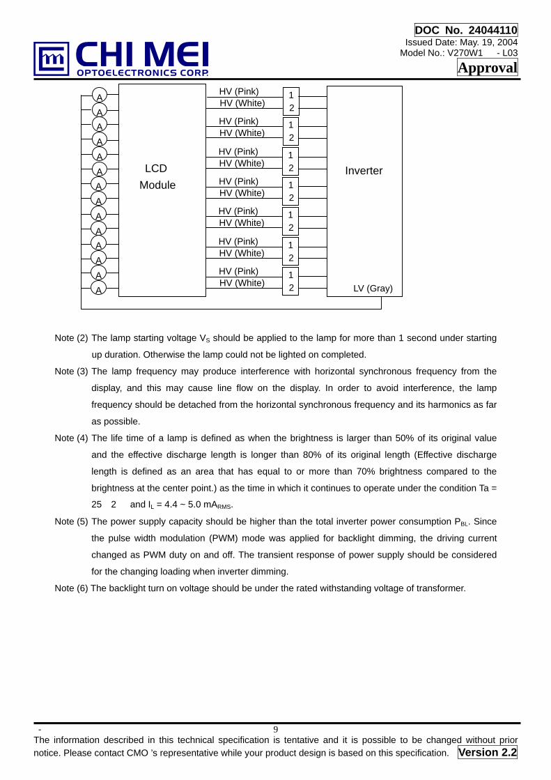
e Inverter
1HV (Pink)
2HV (White)
1HV (Pink)
2HV (White)
1HV (Pink)
2HV (White)
1HV (Pink)
2HV (White)
1HV (Pink)
2HV (White)
1HV (Pink)
2HV (White)
1HV (Pink)
2HV (White)
A A A A A A A A A A A A A A
Note (2) The lamp starting voltage VS should be applied to the lamp for more than 1 second under starti
up duration. Otherwise the lamp could not be lighted on completed.
Note (3) The lamp frequency may produce interference with horizontal synchronous frequency from t
display, and this may cause line flow on the display. In order to avoid interference, the lam
frequency should be detached from the horizontal synchronous frequency and its harmonics as f
as possible.
Note (4) The life time of a lamp is defined as when the brightness is larger than 50% of its original val
and the effective discharge length is longer than 80% of its original length (Effective dischar
length is defined as an area that has equal to or more than 70% brightness compared to t
brightness at the center point.) as the time in which it continues to operate under the condition Ta
25 ±2℃ and IL = 4.4 ~ 5.0 mARMS.
Note (5) The power supply capacity should be higher than the total inverter power consumption PBL. Sin
the pulse width modulation (PWM) mode was applied for backlight dimming, the driving curre
changed as PWM duty on and off. The transient response of power supply should be consider
for the changing loading when inverter dimming.
Note (6) The backlight turn on voltage should be under the rated withstanding voltage of transformer.
- The information described in this technical specification is tentative and it is possible to be changed withonotice. Please contact CMO ’s representative while your product design is based on this specification. Versio
9
LCD Modul
LV (Gray)
ng
he
p
ar
ue
ge
he
=
ce
nt
ed
ut prior n 2.2

DOC No. 24044110 Issued Date: May. 19, 2004
Model No.: V270W1 - L03
Approval
3.2.3 INVERTER INTERTFACE CHARACTERISTICS
Item Symbol Test Condition Min. Typ. Max. Unit Note
ON - 2.0 - 5.0 V On/Off Control Voltage OFF
VBLON - 0 - 0.8 V
HI - 2.0 - 5.0 V Internal/External PWM Select Voltage LO
VSEL - 0 - 0.8 V
MAX - - 3.0 V minimum duty ratio Internal PWM Control Voltage MIN
VIPWM VSEL = L - 0 - V maximum duty ratio
HI 2.0 - 5.0 V duty on External PWM Control Voltage LO
VEPWM VSEL = H 0 - 0.8 V duty off
Control Signal Rising Time Tr - - - 100 ms
Control Signal Falling Time Tf - - - 100 ms
PWM Signal Rising Time TPWMR - - - 50 us
PWM Signal Falling Time TPWMF - - - 50 us Input impedance RIN - 1 - - MΩ
BLON Delay Time Ton - 300 - 500 ms
BLON Off Time Toff - 300 - 500 ms
Note (1) The SEL signal should be valid before backlight turns on by BLON signal. It is inhibited to change
the internal/external PWM selection (SEL) during backlight turn on period.
Note (2) The power sequence and control signal timing are shown as the following figure.
- The information described in this technical specification is tentative and it is possible to be changed without prior notice. Please contact CMO ’s representative while your product design is based on this specification. Version 2.2
10

DOC No. 24044110 Issued Date: May. 19, 2004
Model No.: V270W1 - L03
Approval
2.0V0.8V
Tr TfBacklight on duration
0
VEPWM
3.0VVIPWM
TPWMR
VW
Ext. Dimming FunctionInt. Dimming Function
Ton
Minimun Duty
100%
ExternalPWM Duty
VBL
VBLON
VSEL
0
0
0
0
2.0V0.8V
2.0V0.8V
TPWMF
Toff
ExternalPWMPeriod
- The information described in this technical specification is tentative and it is possible to be changed without prior notice. Please contact CMO ’s representative while your product design is based on this specification. Version 2.2
11

DOC No. 24044110 Issued Date: May. 19, 2004
Model No.: V270W1 - L03
Approval
4. BLOCK DIAGRAM 4.1 TFT LCD MODULE
TFT LCD PANEL
(1280x3x720)
DATA DRIVER IC
SCA
N D
RIVER
IC
LVDS INPUT /
OVER DRIVING CONTROLLER /
TIMING CONTROLLER
I
NPU
T CO
NN
ECTO
R(JA
E-FI-SE30P-HF)
LAMP CONNECTO
VL
- The information described in this technnotice. Please contact CMO ’s represent
DC/DC CONVERTER &
REFERENCE VOLTAGE
GND
Vcc
RX0(+/-)
RX1(+/-)
RX2(+/-)
RX3(+/-)
RXC(+/-)
BACKLIGHT UNITR
ical specification is tentative and it is possible to be changed without prior ative while your product design is based on this specification. Version 2.2
12

DOC No. 24044110 Issued Date: May. 19, 2004
Model No.: V270W1 - L03
Approval
5. INPUT TERMINAL PIN ASSIGNMENT 5.1 TFT LCD MODULE
Pin Name Description 1 NC No Connection 2 NC No Connection 3 NC No Connection 4 NC No Connection 5 NC No Connection 6 NC No Connection 7 NC No Connection 8 GND Ground 9 RX3+ Positive LVDS differential data input. Channel 3
10 RX3- Negative LVDS differential data input. Channel 3 11 RXCLK+ Positive LVDS differential clock input. 12 RXCLK- Negative LVDS differential clock input. 13 GND Ground 14 GND Ground 15 RX2+ Positive LVDS differential data input. Channel 2 16 RX2- Negative LVDS differential data input. Channel 2 17 RX1+ Positive LVDS differential data input. Channel 1 18 RX1- Negative LVDS differential data input. Channel 1 19 RX0+ Positive LVDS differential data input. Channel 0 20 RX0- Negative LVDS differential data input. Channel 0 21 GND Ground 22 GND Ground 23 GND Ground 24 GND Ground I25 GND Ground 26 VCC +5.0V power supply 27 VCC +5.0V power supply 28 VCC +5.0V power supply 29 VCC +5.0V power supply 30 VCC +5.0V power supply
Note (1) Connector Part No.: FI-SE30P-HF (JAE)
Note (2) The first pixel is even.
- The information described in this technical specification is tentative and it is possible to be changed without prior notice. Please contact CMO ’s representative while your product design is based on this specification. Version 2.2
13

DOC No. 24044110 Issued Date: May. 19, 2004
Model No.: V270W1 - L03
Approval
5.2 BACKLIGHT UNIT The pin configuration for the housing and leader wire is shown in the table below.
CN3-CN9 (Housing): BHR-03VS-1 Pin Name Description Wire Color 1 HV High Voltage Pink 2 HV High Voltage White
Note (1) The backlight interface housing for high voltage side is a model BHR-03VS-1, manufactured by JST.
The mating header on inverter part number is SM02(8.0)B-BHS-1-TB.
CN10 (Housing): ZHR-2 or equivalent Pin Name Description Wire Color 1 LV Low Voltage Gray 2 NC - -
Note (2) The backlight interface housing and return cable for low voltage side is a model ZHR-2 or equivalent,
manufactured by JST or equivalent. The mating header on inverter part number is S2B-ZR-SM3A-TF
or equivalent. RETURN CABLE
2 HV(Wh
2 HV(Wh
1 HV(Pin
1 HV(Pin
2 HV(Wh
LV (Gray)
- The information described in this technical specification is tentative and it is possible to be chanotice. Please contact CMO ’s representative while your product design is based on this specificatio
14
ite)
ite)
k)
k)
ite)
nged without prior n. Version 2.2

DOC No. 24044110 Issued Date: May. 19, 2004
Model No.: V270W1 - L03
Approval
5.3 INVERTER UNIT CN1(Header):S10B-PH-SM3-TB(JST) or equivalent.
Pin Name Description 1 2 3 4 5
VBL +24V Power input
6 7 8 9
10
GND Ground
CN2(Header): S12B-PH-SM3-TB(JST) or equivalent. Pin Name Description 1 2 3 4 5
VBL +24V Power input
6 7 8
GND Ground
9 SEL Internal/external PWM selection High : external dimming Low : internal dimming
10 E_PWM External PWM control signal E_PWM should be connected to low when internal PWM was selected (SEL = low).
11 I_PWM Internal PWM control signal I_PWM should be connected to ground when external PWM was selected (SEL = high).
12 BLON Backlight on/off control
CN3-CN9(Header): SM02(8.0)B-BHS-1-TB(JST) Pin Name Description 1 CCFL HOT CCFL high voltage 2 CCFL HOT CCFL high voltage
CN10(Header): S2B-ZR-SM3A-TF(JST) or equivalent Pin Name Description 1 CCFL COLD CCFL low voltage 2 NC -
Note (1) Floating of any control signal is not allowed.
- The information described in this technical specification is tentative and it is possible to be changed without prior notice. Please contact CMO ’s representative while your product design is based on this specification. Version 2.2
15

DOC No. 24044110 Issued Date: May 19, 2004
Model No.: V270W - L03
Approval 5.4 BLOCK DIAGRAM OF INTERFACE
CNF1
100pF
R0~R7
G0~G7
B0~B7
DE
Notes: 1)
2)
The informnotice. Pleas
R0-R7
100pF7 7
G0-Ge
B0-B7
100pF
Th
LV
us
ati c
DE
Rx3+100pF
00pF
Host Graphics Controller
: Pixel
: Pixel
: Pixel
: Displ
e syste
DS ca
ed diffe
on desontact
TxIN
R Data
G Data
B Data
ay timing s
m must h
ble impeda
rentially.
cribed in tCMO ’s re
PLL
ignal
ave the transmitter to drive the module.
nce shall be 50 ohms per signal line or abou
16 / 30 his technical specification is tentative and itpresentative while your product design is bas
PLL
t 100 ohms per
is possible to bed on this speci
R0-R7
G0-G
B0-B7
DE
r
t
DCLK Timing Controlle
LVDS Transmitter THC63LVDM83A (LVDF83A)
LVDS Receiver THC63LVDF84A
Rx0+
Rx0-
Rx1+
Rx1-Rx2+
Rx2-CLK+
CLK-RxOUT
51Ω51Ω
51Ω51Ω
51Ω51Ω
51Ω51Ω
51Ω
51Ω
1
Rx3-
wist-pair line when it is
e changed without prior fication. Version 2.2

DOC No. 24044110 Issued Date: May 19, 2004
Model No.: V270W - L03
Approval 5.5 LVDS INTERFACE
TRANSMITTER THC63LVDM83A INTERFACE CONNECTOR RECEIVER
THC63LVDF84A
SIGNAL PIN INPUT Host TFT-LCD PIN OUTPUT
TFT CONTROL INPUT
R0 R1 R2 R3 R4 R5 G0 G1 G2 G3 G4 G5 B0 B1 B2 B3 B4 B5 DE R6 R7 G6 G7 B6 B7
RSVD 1 RSVD 2 RSVD 3
51 52 54 55 56 3 4 6 7 11 12 14 15 19 20 22 23 24 30 50 2 8
10 16 18 25 27 28
TxIN0 TxIN1 TxIN2 TxIN3 TxIN4 TxIN6 TxIN7 TxIN8 TxIN9
TxIN12 TxIN13 TxIN14 TxIN15 TxIN18 TxIN19 TxIN20 TxIN21 TxIN22 TxIN26 TxIN27 TxIN5
TxIN10 TxIN11 TxIN16 TxIN17 TxIN23 TxIN24 TxIN25
TA OUT0+
TA OUT0-
TA OUT1+
TA OUT1-
TA OUT2+
TA OUT2-
TA OUT3+
TA OUT3-
Rx 0+
Rx 0-
Rx 1+
Rx 1-
Rx 2+
Rx 2-
Rx 3+
Rx 3-
27293032333537383943454647515354551 6 7
34414249502 3 5
Rx OUT0 Rx OUT1 Rx OUT2 Rx OUT3 Rx OUT4 Rx OUT6 Rx OUT7 Rx OUT8 Rx OUT9
Rx OUT12 Rx OUT13 Rx OUT14 Rx OUT15 Rx OUT18 Rx OUT19 Rx OUT20 Rx OUT21 Rx OUT22 Rx OUT26 Rx OUT27 Rx OUT5
Rx OUT10 Rx OUT11 Rx OUT16 Rx OUT17 Rx OUT23 Rx OUT24 Rx OUT25
R0 R1 R2 R3 R4 R5 G0 G1 G2 G3 G4 G5 B0 B1 B2 B3 B4 B5 DE R6 R7 G6 G7 B6 B7
Not connectNot connectNot connect
24bit
DCLK 31 TxCLK IN TxCLK OUT+TxCLK OUT-
RxCLK IN+RxCLK IN-
26 RxCLK OUT DCLK
R0~R7: Pixel R Data (7; MSB, 0; LSB)
G0~G7: Pixel G Data (7; MSB, 0; LSB)
B0~B7: Pixel B Data (7; MSB, 0; LSB)
DE : Display timing signal
Notes: 1)RSVD(reserved)pins on the transmitter shall be “H” or “L”.
17 / 30 The information described in this technical specification is tentative and it is possible to be changed without prior notice. Please contact CMO ’s representative while your product design is based on this specification. Version 2.2

DOC No. 24044110 Issued Date: May 19, 2004
Model No.: V270W - L03
Approval 5.6 COLOR DATA INPUT ASSIGNMENT
The brightness of each primary color (red, green and blue) is based on the 8-bit gray scale data input for
the color. The higher the binary input, the brighter the color. The table below provides the assignment of
color versus data input. Data Signal
Red Green Blue Color R7 R6 R5 R4 R3 R2 R1 R0 R7 R6 G5 G4 G3 G2 G1 G0 R7 R6 B5 B4 B3 B2 B1 B0
Basic Colors
Black Red Green Blue Cyan Magenta Yellow White
01000111
0 1 0 0 0 1 1 1
0 1 0 0 0 1 1 1
0 1 0 0 0 1 1 1
01000111
01000111
01000111
01000111
00101011
00101011
00101011
00101011
00101011
00101011
00101011
0 0 1 0 1 0 1 1
0 0 0 1 1 1 0 1
0 0 0 1 1 1 0 1
0 0 0 1 1 1 0 1
0 0 0 1 1 1 0 1
00011101
00011101
00011101
00011101
Gray Scale Of Red
Red(0) / Dark Red(1) Red(2)
: :
Red(253) Red(254) Red(255)
000::111
0 0 0 : : 1 1 1
0 0 0 : : 1 1 1
0 0 0 : : 1 1 1
000::111
000::111
001::011
010::101
000::000
000::000
000::000
000::000
000::000
000::000
000::000
0 0 0 : : 0 0 0
0 0 0 : : 0 0 0
0 0 0 : : 0 0 0
0 0 0 : : 0 0 0
0 0 0 : : 0 0 0
000::000
000::000
000::000
000::000
Gray Scale Of Green
Green(0) / Dark Green(1) Green(2)
: :
Green(253) Green(254) Green(255)
000::000
0 0 0 : : 0 0 0
0 0 0 : : 0 0 0
0 0 0 : : 0 0 0
000::000
000::000
000::000
000::000
000::111
000::111
000::111
000::111
000::111
000::111
001::011
0 1 0 : : 1 0 1
0 0 0 : : 0 0 0
0 0 0 : : 0 0 0
0 0 0 : : 0 0 0
0 0 0 : : 0 0 0
000::000
000::000
000::000
000::000
Gray Scale Of Blue
Blue(0) / Dark Blue(1) Blue(2)
: :
Blue(253) Blue(254) Blue(255)
000::000
0 0 0 : : 0 0 0
0 0 0 : : 0 0 0
0
0 : : 0 0 0
000::000
000::000
000::000
000::000
000::000
000::000
000::000
000::000
000::000
000::000
000::000
0 0 0 : : 0 0 0
0 0 0 : : 1 1 1
0 0 0 : : 1 1 1
0 0 0 : : 1 1 1
0 0 0 : : 1 1 1
000::111
000::111
001::011
010::101
0
Note (1) 0: Low Level Voltage, 1: High Level Voltage
18 / 30 The information described in this technical specification is tentative and it is possible to be changed without prior notice. Please contact CMO ’s representative while your product design is based on this specification. Version 2.2

DOC No. 24044110 Issued Date: May 19, 2004
Model No.: V270W - L03
Approval 6. INTERFACE TIMING
6.1 INPUT SIGNAL TIMING SPECIFICATIONS The input signal timing specifications are shown as the following table and timing diagram.
Signal Item Symbol Min. Typ. Max. Unit Note Clock Frequency 1/Tc 70 74.25 80 MHZ -
Frame Rate Fr 48 60 - Hz Tv=Tvd+TvbTotal Tv 730 750 850 Th - Display Tvd 720 720 720 Th - Vertical Active Display Term
Blank Tvb 10 30 130 Th - Total Th 1450 1650 2000 Tc Th=Thd+ThbDisplay Thd 1280 1280 1280 Tc - Horizontal Active Display Term Blank Thb 170 370 720 Tc -
Note: Because of this module is operated by DE only mode, Hsync and Vsync input signals should be set
to low logic level or ground. Otherwise, this module would operate abnormally.
INPUT SIGNAL TIMING DIAGRAM
DATA
DE
Thd
DCLK
Tc
Valid display data (1280 clocks)
Thb
DE
Th
Tv
Tvb Tvd
19 / 30 The information described in this technical specification is tentative and it is possible to be changed without prior notice. Please contact CMO ’s representative while your product design is based on this specification. Version 2.2

DOC No. 24044110 Issued Date: May 19, 2004
Model No.: V270W - L03
Approval 6.2 POWER ON/OFF SEQUENCE To prevent a latch-up or DC operation of LCD module, the power on/off sequence should be as the diagram below.
0≦T1≦10ms 0≦T2≦50ms 0≦T3≦50ms 1s≦T4
50%
0V
0V
50%
T6 T5
T3 T1
0.1VDD
0.9 VCC
0.1VCC
0.9 VCC
T4 T2
VALID
Power On
Power Supply
VCC
Signals
Power Off
Backlight (Recommended) 450ms≦T5 100ms≦T6
Power ON/OFF Sequence
Note.
(1) The supply voltage of the external system for the module input should be the same as the definition of Vcc.
(2) Apply the lamp voltage within the LCD operation range. When the backlight turns on before the LCD operation of
the LCD turns off before the backlight turns off, the display may momentarily become abnormal screen.
(3) In case of VCC = off level, please keep the level of input signals on the low or keep a high impedance.
(4) T4 should be measured after the module has been fully discharged between power of and on period.
(5) Interface signal shall not be kept at high impedance when the power is on.
20 / 30 The information described in this technical specification is tentative and it is possible to be changed without prior notice. Please contact CMO ’s representative while your product design is based on this specification. Version 2.2

DOC No. 24044110 Issued Date: May 19, 2004
Model No.: V270W - L03
Approval 7. OPTICAL CHARACTERISTICS
7.1 TEST CONDITIONS Item Symbol Value Unit
Ambient Temperature Ta 25±2 oC Ambient Humidity Ha 50±10 %RH Supply Voltage VCC 5.0 V Input Signal According to typical value in "3. ELECTRICAL CHARACTERISTICS" Lamp Current IL 4.7±0.3 mA Oscillating Frequency (Inverter) FW 56±2 KHz
7.2 OPTICAL SPECIFICATIONS
The relative measurement methods of optical characteristics are shown in 7.2. The following items should
be measured under the test conditions described in 7.1 and stable environment shown in Note (7). Item Symbol Condition Min. Typ. Max. Unit Note
Contrast Ratio CR 400 600 - - Note(2) TR - 15 25 ms TF - 10 20 ms
Note(3) Response Time
Gray to gray 16.6 ms Note(4)
Center Luminance of White LC 450 550 - cd/m2 Note(5) Average Luminance of White LAVE 400 450 - cd/m2 White Variation δW - - 1.6 - Note(8) Cross Talk CT - - 4.0 % Note(6)
Rx 0.616 0.646 0.676 - Red Ry 0.302 0.332 0.362 - Gx 0.239 0.269 0.299 - Green Gy 0.570 0.600 0.630 - Bx 0.112 0.142 0.172 - Blue By 0.042 0.072 0.102 -
Wx 0.255 0.285 0.315 -
Color Chromaticity
White Wy
θx=0°, θY =0° Viewing Normal Angle
0.263 0.293 0.323 - 9, 300K
θx+ 80 85 - Horizontal θx- 80 85 - θY+ 80 85 -
Viewing Angle
Vertical θY-
CR≥10
80 85 -
Deg. No gray
scale inversion
21 / 30 The information described in this technical specification is tentative and it is possible to be changed without prior notice. Please contact CMO ’s representative while your product design is based on this specification. Version 2.2

DOC No. 24044110 Issued Date: May 19, 2004
Model No.: V270W - L03
Approval Note (1) Definition of Viewing Angle (θx, θy):
Viewing angles are measured by Eldim EZ-Contrast 160R
θX- = 90º
θX+ = 90º
Normal
θx = θy = 0º
x+ y-
y+x-
θy+ θy-
θx+ θx−
6 o’clock
θy- = 90º
12 o’clock direction
θy+ = 90º
Note (2) Definition of Contrast Ratio (CR):
The contrast ratio can be calculated by the following expression.
Contrast Ratio (CR) = L255 / L0
L255: Luminance of gray level 255
L 0: Luminance of gray level 0
CR = CR (5)
CR (X) is corresponding to the Contrast Ratio of the point X at the figure in Note (8).
Note (3) Definition of Response Time (TR, TF):
TRTF Time
Gray Level 255
Gray Level 0
Gray Level 255
Optical
Response
100%
90%
10%
0%
22 / 30 The information described in this technical specification is tentative and it is possible to be changed without prior notice. Please contact CMO ’s representative while your product design is based on this specification. Version 2.2

DOC No. 24044110 Issued Date: May 19, 2004
Model No.: V270W - L03
Approval Note (4) Definition of Gray to Gray Switching Time:
Optical
Response
100%90%
10%0%
Gray to gray switching time
Time
Time Gray to gray switching time
Drive signal
of LCD Panel
The driving signal means the signal of gray level 0,63,127,191,255.
Note (5) Definition of Luminance of White (LC, LAVE):
Measure the luminance of gray level 255 at center point and 5 points
LC = L (5)
LAVE = [L (1)+ L (2)+ L (3)+ L (4)+ L (5)] / 5
L (x) is corresponding to the luminance of the point X at the figure in Note (8).
Note (6) Definition of Cross Talk (CT):
CT = | YB – YA | / YA × 100 (%)
Where:
YA = Luminance of measured location without gray level 0 pattern (cd/m2)
YB = Luminance of measured location with gray level 0 pattern (cd/m2)
(0, 0)
YA, L (D/8,W/2)
YA, D (D/2,7W/8)
a a
The information describnotice. Please contact CMO
Active Are
Gray 128
YA, U (D/2,W/8) YB, U (D/2,W/8)
0
(D/4,W/4)
YB, R (7D/8,W/2)YB, L (D/8,W/2)
ed in this technica ’s representative
Y (7D/8,W/2)
A, R(3D/4,3W/4)
YB, D (D/2,7W/8)
(D,W)
23 / 30 l specification is tentative and it i while your product design is base
Active Are
s d
Gray
(0, 0)
)
possible to be ch on this specificati
(D,W
Gray 128
0 Gray
anged without prior on. Version 2.2

DOC No. 24044110 Issued Date: May 19, 2004
Model No.: V270W - L03
Approval Note (7) Measurement Setup:
The LCD module should be stabilized at given temperature for 1 hour to avoid abrupt
temperature change during measuring. In order to stabilize the luminance, the measurement
should be executed after lighting Backlight for 1 hour in a windless room.
Light Shield Room
(Ambient Luminance < 2 lux)
Display Color Analyzer (Minolta CA210)
Center of the Screen
LCD Panel
LCD Module
Note (8) Definition of White Variation (δW):
Measure the luminance of gray level 255 at 5 points
δW = Maximum [L (1), L (2), L (3), L (4), L (5)] / Minimum [L (1), L (2), L (3), L (4), L (5)]
Horizontal Line
X
3W/4
W/2
W/4
3D/4D/2D/4
43
21
5 : Test Point
X=1 to 5 W
D
Verti
cal L
ine
Active Area
24 / 30 The information described in this technical specification is tentative and it is possible to be changed without prior notice. Please contact CMO ’s representative while your product design is based on this specification. Version 2.2
DOC No. 24044110 Issued Date: May 19, 2004
Model No.: V270W - L03
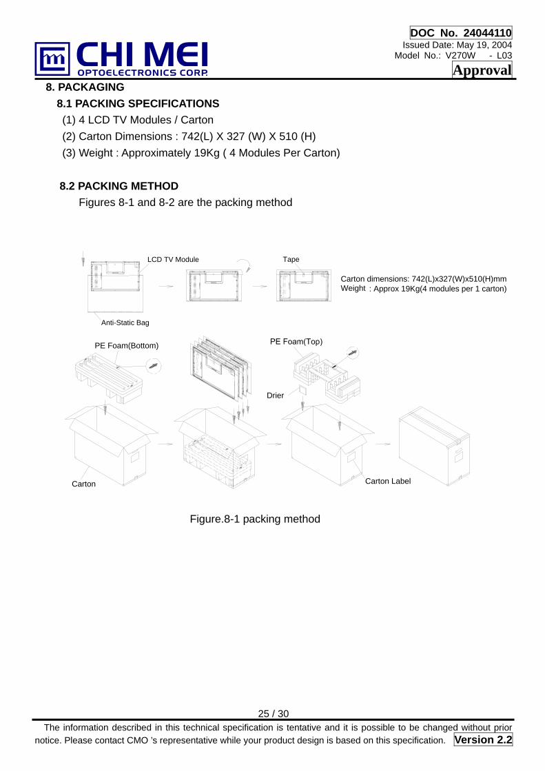
Approval 8. PACKAGING 8.1 PACKING SPECIFICATIONS
(1) 4 LCD TV Modules / Carton (2) Carton Dimensions : 742(L) X 327 (W) X 510 (H) (3) Weight : Approximately 19Kg ( 4 Modules Per Carton) 8.2 PACKING METHOD Figures 8-1 and 8-2 are the packing method
LCD TV Module
Anti-Static Bag
Drier
Carton Label
: Approx 19Kg(4 modules per 1 carton)Carton dimensions: 742(L)x327(W)x510(H)mmWeight
Carton
PE Foam(Bottom)
Tape
Figure.8-1 packing method
25 / 30 The information described in this technical specification is tentative and it is possible to be changed without prior notice. Please contact CMO ’s representative while your product design is based on this specification. Version 2.2

DOC No. 24044110 Issued Date: May 19, 2004
Model No.: V270W - L03
Approval
Corner Protector:L1020*50mm*50mmPallet:L1100*W1100*H135mm
Pallet Stack:L1100*W1100*H1163mmGross Weight:180kg
Carton Label
Bottom Cap
PP Belt
Film
Bottom Cap:L1100*W1100*H120mm
PE Sheet
Figure. 8-2 packing method
26 / 30 The information described in this technical specification is tentative and it is possible to be changed without prior notice. Please contact CMO ’s representative while your product design is based on this specification. Version 2.2

DOC No. 24044110 Issued Date: May 19, 2004
Model No.: V270W - L03
Approval 9. DEFINITION OF LABELS
9.1 CMO MODULE LABEL The barcode nameplate is pasted on each module as illustration, and its definitions are as following explanation.
(a) Model Name: V270W1-L03
(b) Revision: Rev. XX, for example: A0, A1… B1, B2… or C1, C2…etc.
(c) Serial ID: X X X X X X X Y M D L N N N N
Product Line
Year, Month, Date
Serial No.
CHI MEI OPTOELECTRONICS MADE IN TAIWAN
E207943
X X X X X X X Y M D L N N N N
MADE IN TAIWAN V270W1 -L03 Rev. XX
CMO Internal Use
CMO Internal Use
Revision
CMO Internal Use Serial ID includes the information as below:
(a) Manufactured Date: Year: 0~9, for 2000~2009
Month: 1~9, A~C, for Jan. ~ Dec.
Day: 1~9, A~Y, for 1st to 31st, exclude I ,O, and U.
(b) Revision Code: Cover all the change
(c) Serial No.: Manufacturing sequence of product
(d) Product Line: 1 -> Line1, 2 -> Line 2, …etc.
27 / 30 The information described in this technical specification is tentative and it is possible to be changed without prior notice. Please contact CMO ’s representative while your product design is based on this specification. Version 2.2
DOC No. 24044110 Issued Date: May 19, 2004
Model No.: V270W - L03
Approval 10. PRECAUTIONS
10.1 ASSEMBLY AND HANDLING PRECAUTIONS (1) Do not apply rough force such as bending or twisting to the module during assembly.
(2) It is recommended to assemble or to install a module into the user’s system in clean working areas.
The dust and oil may cause electrical short or worsen the polarizer.
(3) Do not apply pressure or impulse to the module to prevent the damage of LCD panel and Backlight.
(4) Always follow the correct power-on sequence when the LCD module is turned on. This can prevent the
damage and latch-up of the CMOS LSI chips.
(5) Do not plug in or pull out the I/F connector while the module is in operation.
(6) Do not disassemble the module.
(7) Use a soft dry cloth without chemicals for cleaning, because the surface of polarizer is very soft and
easily scratched.
(8) Moisture can easily penetrate into LCD module and may cause the damage during operation.
(9) High temperature or humidity may deteriorate the performance of LCD module. Please store LCD
modules in the specified storage conditions.
(10) When ambient temperature is lower than 10ºC, the display quality might be reduced. For example, the
response time will become slow, and the starting voltage of CCFL will be higher than that of room
temperature.
10.2 SAFETY PRECAUTIONS (1) The startup voltage of a Backlight is approximately 1000 Volts. It may cause an electrical shock while
assembling with the inverter. Do not disassemble the module or insert anything into the Backlight unit.
(2) If the liquid crystal material leaks from the panel, it should be kept away from the eyes or mouth. In
case of contact with hands, skin or clothes, it has to be washed away thoroughly with soap.
(3) After the module’s end of life, it is not harmful in case of normal operation and storage.
28 / 30 The information described in this technical specification is tentative and it is possible to be changed without prior notice. Please contact CMO ’s representative while your product design is based on this specification. Version 2.2

DOC No. 24044110 Issued Date: May 19, 2004
Model No.: V270W - L03
Approval 11. MECHANICAL CHARACTERISTICS
29 / 30 The information described in this technical specification is tentative and it is possible to be changed without prior notice. Please contact CMO ’s representative while your product design is based on this specification. Version 2.2

DOC No. 24044110 Issued Date: May 19, 2004
Model No.: V270W - L03
Approval
30 / 30
The information described in this technical specification is tentative and it is possible to be changed without prior notice. Please contact CMO ’s representative while your product design is based on this specification. Version 2.2