Embed Size (px)
Citation preview
THAN0196_Rev.1.30_E
Copyright© 2016 THine Electronics, Inc. 1/26 THine Electronics, Inc. Security E
Application Note THAN0196_Rev.1.30_E
THCV231(-Q)/THCV236(-Q) Application Note
System Diagram, Register Setting and PCB Design Guideline
THAN0196_Rev.1.30_E
Copyright© 2016 THine Electronics, Inc. 2/26 THine Electronics, Inc. Security E
Contents
Contents .................................................................................................................................................................. 2
Application Diagram ............................................................................................................................................. 3
RAW12bit per pixel falling edge system ........................................................................................................................... 3
YCbCr8bit bus-width rising edge system ......................................................................................................................... 4
Signaling Usage ...................................................................................................................................................... 5
Example Connection 1: Sharing Power Supply ............................................................................................................... 5
Sub-Link Communication .................................................................................................................................... 6
Sub-Link Notification ........................................................................................................................................................ 6
Example Operation 1-1: Access to Sub-Link Master Device Register ........................................................................... 7
Example Operation 1-2: Access to Sub-Link Slave Device Register .............................................................................. 9
Example Operation 1-3: Access to 2-wire serial Slave Device with 8bit Register Address ......................................... 12
Example Operation 1-4: Access to 2-wire serial Slave Device with 16bit Register Address ....................................... 14
Example Operation 2-1: Through GPIO Sub-Link Master to Sub-Link Slave .......................................................... 16
Example Operation 2-2: Programmable GPIO output control .................................................................................... 17
Example Operation 2-3: Programmable GPIO input control ...................................................................................... 18
Example Operation 3-1: Interrupt feedback as internal factor .................................................................................... 19
Example Operation 3-2: Interrupt output as external factor by Slave side ................................................................ 20
Power Supply Usage ............................................................................................................................................ 21
Power Supply for THCV231(-Q) ..................................................................................................................................... 21
Power Supply for THCV236(-Q) ..................................................................................................................................... 22
PCB layout guideline between VDD (41Pin) and AVDD (40Pin) for THCV236(-Q) ................................................... 23
Note ....................................................................................................................................................................... 24
1) Power On Sequence .............................................................................................................................................. 24
2) Cable Connection and Disconnection ................................................................................................................. 24
3) GND Connection................................................................................................................................................... 24
4) Low Input Pulse into PDN, PDN1 and PDN0 Period Requirement ................................................................. 24
PCB Layout Considerations ............................................................................................................................... 25
Notices and Requests ........................................................................................................................................... 26
THAN0196_Rev.1.30_E
Copyright© 2016 THine Electronics, Inc. 3/26 THine Electronics, Inc. Security E
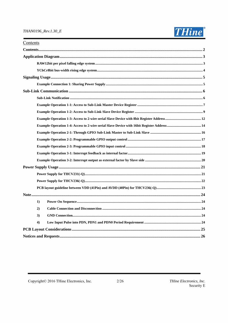
Application Diagram
RAW12bit per pixel falling edge system
GPIO4 and GPIO3 input to the THCV236(-Q) are output from the THCV231(-Q) by through GPIO function in order to send camera reset signal etc.
Set RF pin Low (Falling edge LVCMOS input). BET, BETOUT and LATEN pins can be used as Bit Error Test in actual configuration in order for debug or test
purpose. [THCV231(-Q)]
PDN can be controlled by external resistor or other driving source like MCU. Unused LVCMOS inputs pins should be connected to Low (GND).
[THCV236(-Q)] Set RXDEFSEL pin Low. Default setting is Sync Free Mode for the THCV231(-Q). Sync Free Mode is
suitable to transmitting data of the system without DE sync signal like camera. PDN0 and OE can be controlled by external resistor or other driving source like MCU.
Unused LVCMOS output pins should be left Open. Place 10Ω resistor close to outputs, which can be eliminated when freq. is low and trace is short.
To 2-wire serialSlave Device
0.1uF 0.1uF
10uF
0.1uF
10uF
0.1uF0.1uF
LVCMOS Driver
TxPDWN
LVCMOSReceiver
Damping resistorex. 10ΩClose to THCV236(-Q)
RxPDWN
RxBETset
OEset
TxPDWN
1kΩ
NC
1kΩ
NC
NC
0Ω
1kΩ
NC
RxPDWN
RxBETset
OEset
SDA
THCV231(-Q)Sub-Link
Slave side
TXN
TXP
CLKIN
H/VSYNC
PDN
SDL
RF/BETOUT
TCMP
TCMN
TEST1
TEST2
CAPOUT
CAPINA
CAPINP
D7-D0
COL1/SD0
THCV236(-Q)Sub-Link
Master side
RXN
RXP
MAINMODE/RCMN
HFSEL/RCMP
LOCKN/MSSEL
HTPDN/SUBMODE
RF/BETOUT
PDN1
RXDEFSEL
BET
OE
PDN0
LFSEL
CAPOUT
CAPINA
TEST1
TEST2
TTLDRV/SD2/AIN0/GPIO1
OUTSEL/SD1
LATEN/SD3/AIN1/GPIO0
COL0/INT/GPIO2
D7-D0
CLKOUT
H/VSYNC
D23-D12
D24/GPIO3
0Ω
NC
0Ω
NC
0.1uF 0.1uF
10kΩ
10kΩ
To MPU (Host Device)
10kΩ
10kΩ
10kΩ
D31-D26
D25/GPIO4RxGPIO4RESET_fromAP
10kΩ
RxGPIO4
10kΩ
When GPIOset input, push pull output or unused, there pull up resistors must be dispensed with.
GPIO4
GPIO3
TxGPIO4
10kΩ
TxGPIO4
10kΩ
When GPIOset input, push pull output or unused, there pull up resistors must be dispensed with.
DE
1kΩ
RxSCL
RxSDA
D11-D8
RAW11-RAW4
RAW3-RAW0
CAM_RESET
CAM_RESET
D11-D8
CAM11-CAM4
CAM3-CAM0
RESET_fromAP
*1 indicates microstrip lines or cables with their differential characteristic impedance being 100 Ω *2 Connect GNDs of both Tx and Rx PCB *3 Field BET Operation. Please see the datasheet for details. (THCV231(-Q)_THCV236(-Q)_Rev.1.00_E.pdf and up)
THAN0196_Rev.1.30_E
Copyright© 2016 THine Electronics, Inc. 4/26 THine Electronics, Inc. Security E
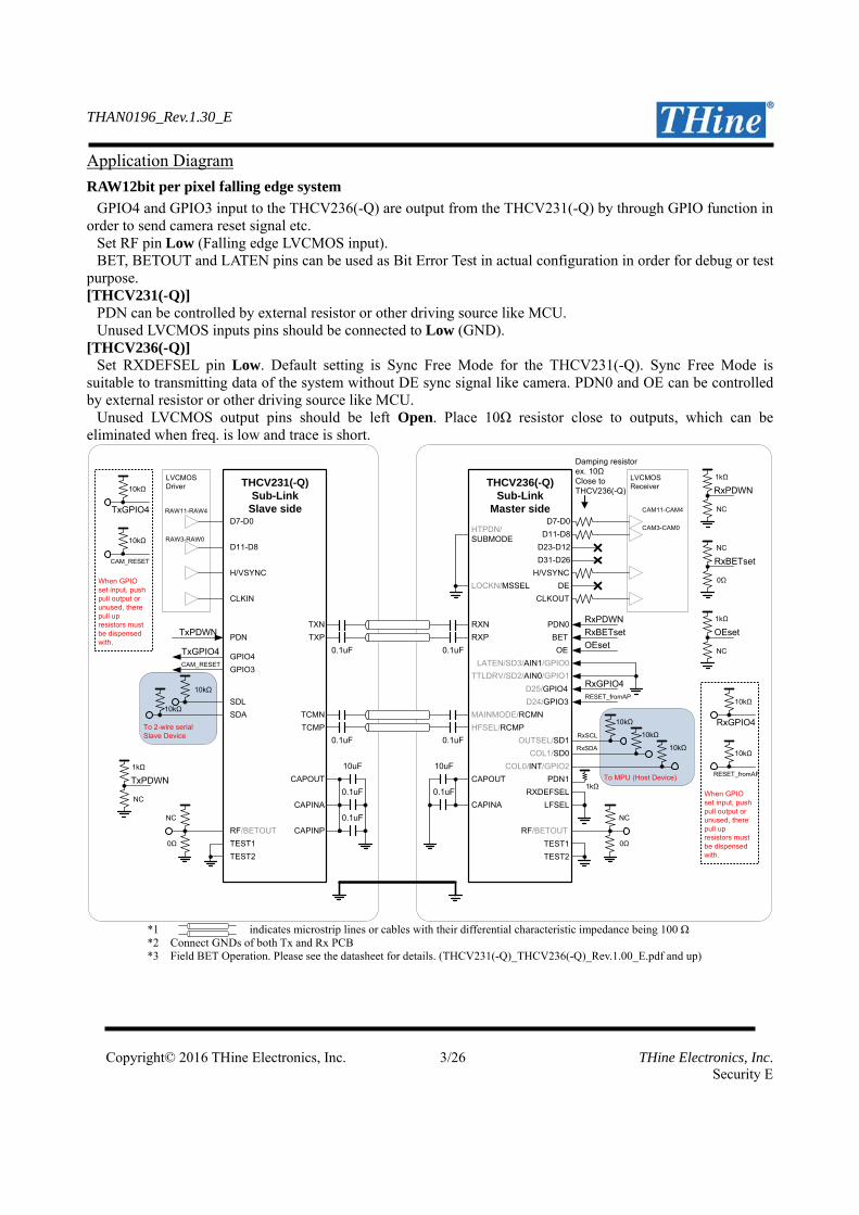
YCbCr8bit bus-width rising edge system
GPIO4 and GPIO3 input to the THCV236(-Q) are output from the THCV231(-Q) by through GPIO function in order to send camera reset signal etc.
Set RF pin High (Rising edge LVCMOS input). BET, BETOUT and LATEN pins can be used as Bit Error Test in actual configuration in order for debug or test
purpose. Note: This case of transmit 8bit or below, CML bit rate can be slowed if set COL1 (Register Name: refer to
page 7 and page 9) to 1 and set COL0 to 0. [THCV231(-Q)]
PDN can be controlled by external resistor or other driving source like MCU. Unused LVCMOS inputs pins should be connected to Low (GND).
[THCV236(-Q)] Set RXDEFSEL pin Low. Default setting is Sync Free Mode for the THCV231(-Q). Sync Free Mode is also
available to transmitting data of embedded sync system without a separate sync signal (ITU656 etc.). PDN0 and OE can be controlled by external resistor or other driving source like MCU.
Unused LVCMOS output pins should be left Open. Place 10Ω resistor close to outputs, which can be eliminated when freq. is low and trace is short.
To 2-wire serialSlave Device
0.1uF 0.1uF
10uF
0.1uF
10uF
0.1uF0.1uF
LVCMOS Driver
TxPDWN
LVCMOSReceiver
Damping resistorex. 10ΩClose to THCV236(-Q)
RxPDWN
RxBETset
OEset
TxPDWN
1kΩ
NC
1kΩ
NC
NC
0Ω
1kΩ
NC
RxPDWN
RxBETset
OEset
SDA
THCV231(-Q)Sub-Link
Slave side
TXN
TXP
CLKIN
H/VSYNC
PDN
SDL
RF/BETOUT
TCMP
TCMN
TEST1
TEST2
CAPOUT
CAPINA
CAPINP
D7-D0
COL1/SD0
THCV236(-Q)Sub-Link
Master side
RXN
RXP
MAINMODE/RCMN
HFSEL/RCMP
LOCKN/MSSEL
HTPDN/SUBMODE
RF/BETOUT
PDN1
RXDEFSEL
BET
OE
PDN0
LFSEL
CAPOUT
CAPINA
TEST1
TEST2
TTLDRV/SD2/AIN0/GPIO1
OUTSEL/SD1
LATEN/SD3/AIN1/GPIO0
COL0/INT/GPIO2
D7-D0
CLKOUT
H/VSYNC
D23-D8
D24/GPIO3
1kΩ
NC
1kΩ
NC
0.1uF 0.1uF
10kΩ
10kΩ
To MPU (Host Device)
10kΩ
10kΩ
10kΩ
D31-D26
D25/GPIO4RxGPIO4
RxGPIO310kΩ
RxGPIO4
10kΩ
RxGPIO3
When GPIOset input, push pull output or unused, there pull up resistors must be dispensed with.
GPIO4
GPIO3TxGPIO3
TxGPIO4
10kΩ
TxGPIO4
10kΩ
TxGPIO3
When GPIOset input, push pull output or unused, there pull up resistors must be dispensed with.
D11-D8
DE
1kΩ
RxSCL
RxSDA
*1 indicates microstrip lines or cables with their differential characteristic impedance being 100 Ω *2 Connect GNDs of both Tx and Rx PCB *3 Field BET Operation. Please see the datasheet for details. (THCV231(-Q)_THCV236(-Q)_Rev.1.00_E.pdf and up)
THAN0196_Rev.1.30_E
Copyright© 2016 THine Electronics, Inc. 5/26 THine Electronics, Inc. Security E
Signaling Usage
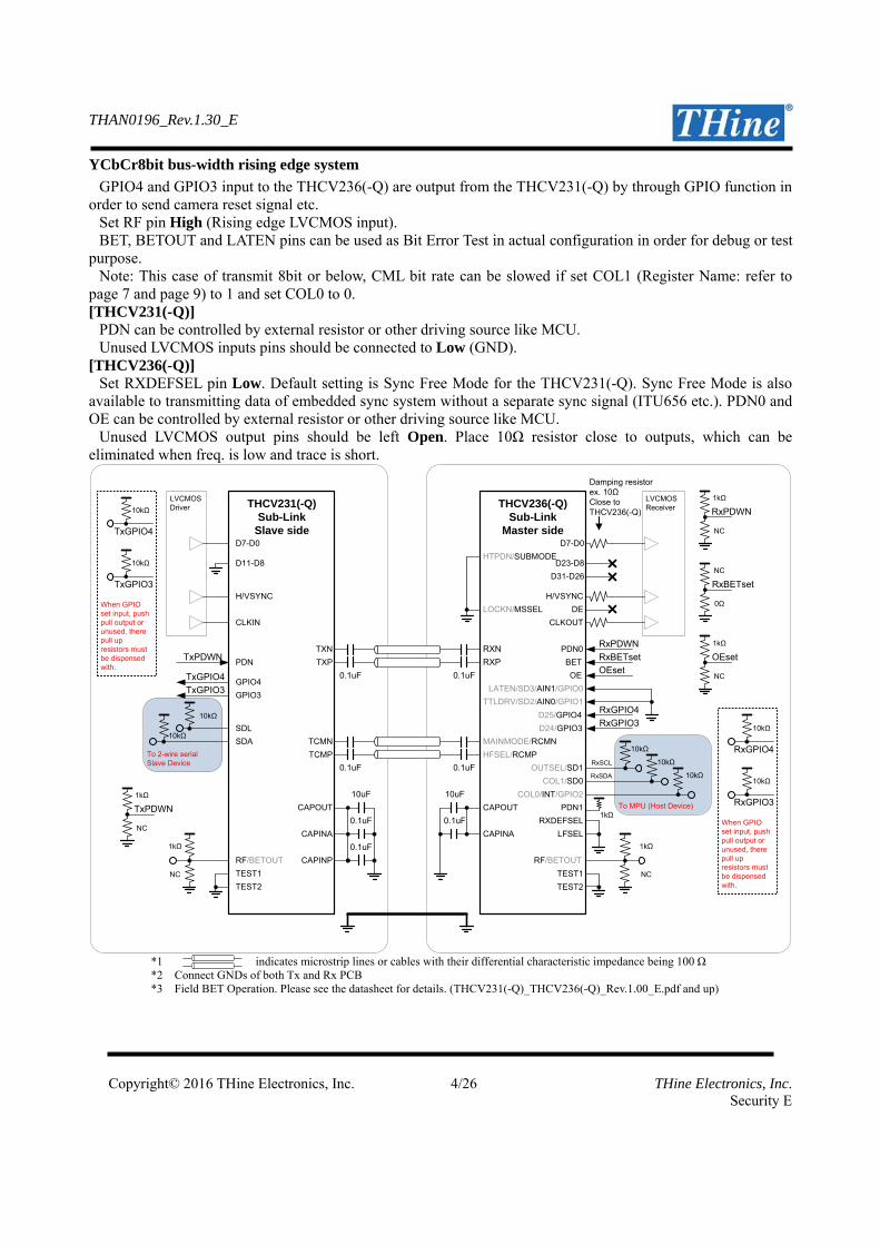
Example Connection 1: Sharing Power Supply
Power supply on common trace is also accomplished by another simple PCB circuit. Put 1uH inductor on both side. Inductor SRF (Self-resonant frequency) should be more than 160MHz. Inductor supply current tolerance must be more than requirement (ex. 500mA). The THCV236(-Q) side AC coupling capacitors must be 100pF.
THAN0196_Rev.1.30_E
Copyright© 2016 THine Electronics, Inc. 6/26 THine Electronics, Inc. Security E
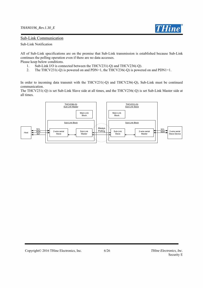
Sub-Link Communication
Sub-Link Notification
All of Sub-Link specifications are on the premise that Sub-Link transmission is established because Sub-Link continues the polling operation even if there are no data accesses. Please keep below conditions.
1. Sub-Link I/O is connected between the THCV231(-Q) and THCV236(-Q). 2. The THCV231(-Q) is powered on and PDN=1, the THCV236(-Q) is powered on and PDN1=1.
In order to incoming data transmit with the THCV231(-Q) and THCV236(-Q), Sub-Link must be continued communication. The THCV231(-Q) is set Sub-Link Slave side at all times, and the THCV236(-Q) is set Sub-Link Master side at all times.
Sub-Link Block
2-wire serialSlave
Host
SCLSDAINT
Sub-LinkMaster
THCV236(-Q)Sub-Link Master
THCV231(-Q)Sub-Link Slave
Sub-Link Block
Sub-LinkSlave
2-wire serial Slave Device
2-wire serial Master
Main-LinkBlock
Main-LinkBlock
AlwaysPolling
SCLSDA
THAN0196_Rev.1.30_E
Copyright© 2016 THine Electronics, Inc. 7/26 THine Electronics, Inc. Security E
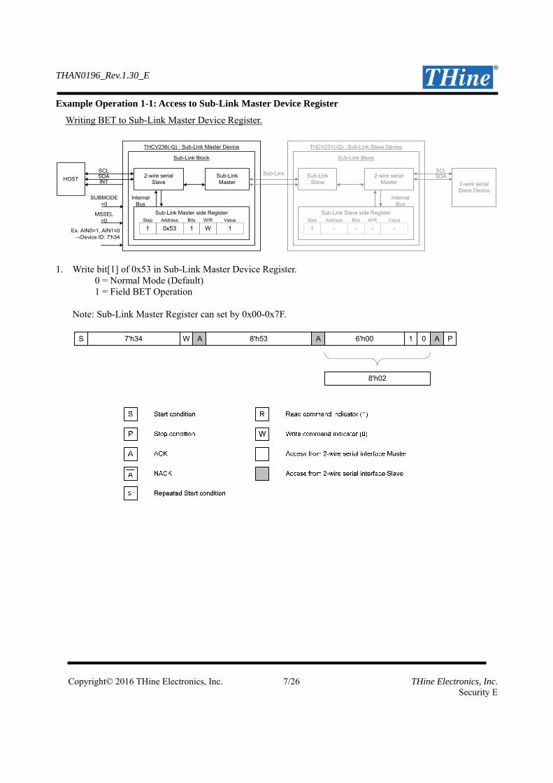
Example Operation 1-1: Access to Sub-Link Master Device Register
Writing BET to Sub-Link Master Device Register.
Sub-Link Block
2-wire serial Slave
HOST
SCLSDA
Sub-Link Master side Register
Sub-LinkMaster
THCV236(-Q) : Sub-Link Master Device THCV231(-Q) : Sub-Link Slave Device
Sub-Link Block
Sub-LinkSlave 2-wire serial
Slave Device
2-wire serial Master
Sub-Link
Internal Bus
Address
0x53 1
Bits Value
1
W/R
W
Step
1
INT
Sub-Link Slave side Register
Internal Bus
Address Bits ValueW/RStep
SCLSDA
1 - -- -
MSSEL=0
Ex. AIN0=1, AIN1=0→Device ID: 7'h34
SUBMODE=0
1. Write bit[1] of 0x53 in Sub-Link Master Device Register.
0 = Normal Mode (Default) 1 = Field BET Operation Note: Sub-Link Master Register can set by 0x00-0x7F.
S 8'h537'h34 W A A 6'h00 A P1
8'h02
0
THAN0196_Rev.1.30_E
Copyright© 2016 THine Electronics, Inc. 8/26 THine Electronics, Inc. Security E
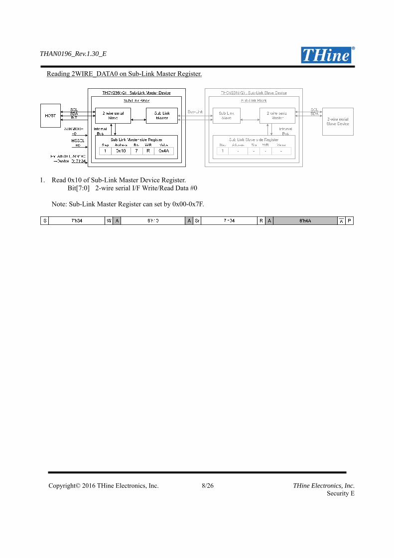
Reading 2WIRE_DATA0 on Sub-Link Master Register.
1. Read 0x10 of Sub-Link Master Device Register.
Bit[7:0] 2-wire serial I/F Write/Read Data #0
Note: Sub-Link Master Register can set by 0x00-0x7F.
THAN0196_Rev.1.30_E
Copyright© 2016 THine Electronics, Inc. 9/26 THine Electronics, Inc. Security E
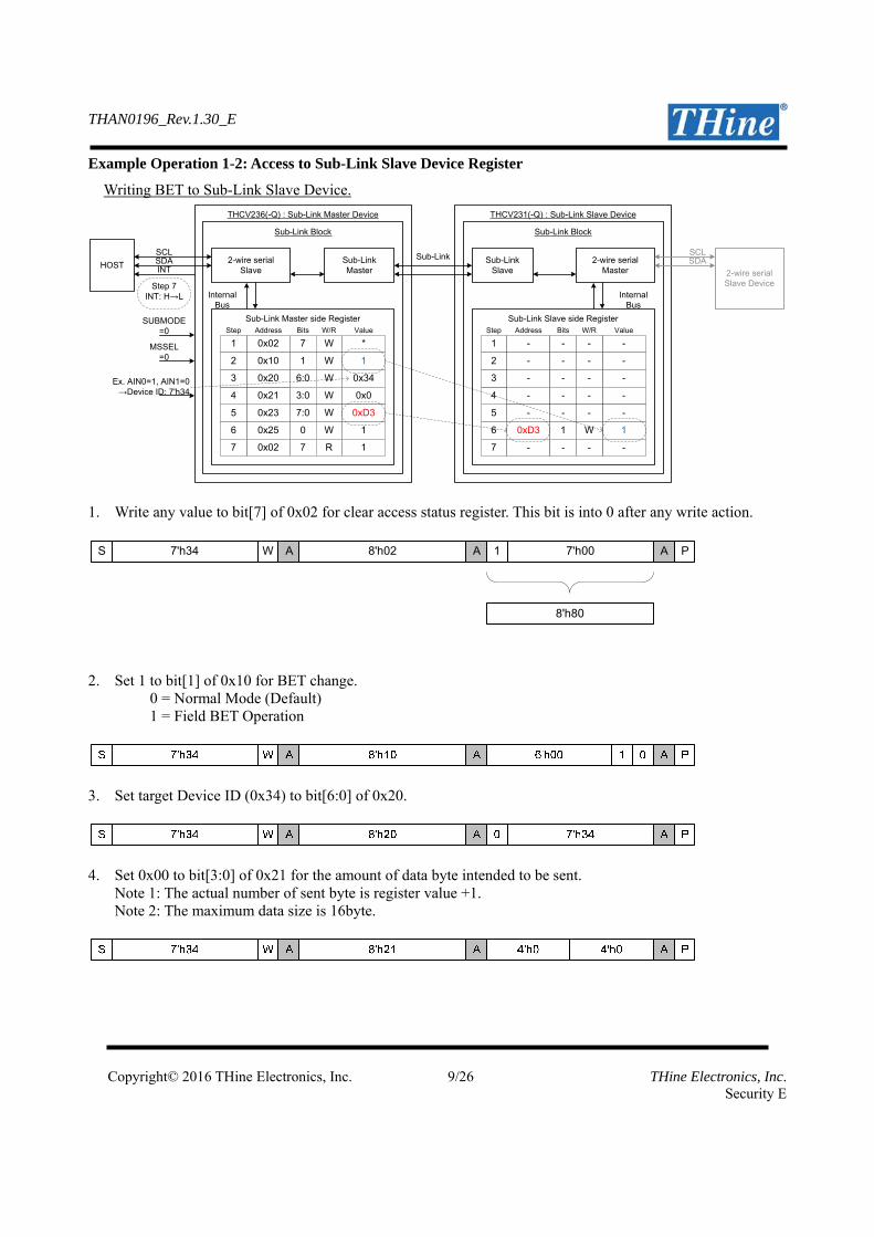
Example Operation 1-2: Access to Sub-Link Slave Device Register
Writing BET to Sub-Link Slave Device.
Sub-Link Block
2-wire serial Slave
HOST
SCLSDA
Sub-Link Master side Register
Sub-LinkMaster
THCV236(-Q) : Sub-Link Master Device THCV231(-Q) : Sub-Link Slave Device
Sub-Link Block
Sub-LinkSlave
2-wire serial Master
Sub-Link
Internal Bus
Address
0x02
0x10
0x25
0x23
*
0x21
0x20
Bits Value
7
W/R
W
Step
1
11 W
0x346:0 W
0x03:0 W
5
4
3
2
6
0xD37:0 W
10 W
0x027 17 R
INT
Sub-Link Slave side Register
Internal Bus
Address
0xD3 1
Bits Value
1
W/R
W
Step
Step 7INT: H→L
SCLSDA
1
5
4
3
2
6
7
- -- -
- -- -
- -- -
- -- -
- -- -
- -- -
MSSEL=0
SUBMODE=0
Ex. AIN0=1, AIN1=0→Device ID: 7'h34
2-wire serial Slave Device
1. Write any value to bit[7] of 0x02 for clear access status register. This bit is into 0 after any write action.
S 8'h027'h34 W A A 7'h00 A P1
8'h80
2. Set 1 to bit[1] of 0x10 for BET change.
0 = Normal Mode (Default) 1 = Field BET Operation
3. Set target Device ID (0x34) to bit[6:0] of 0x20.
4. Set 0x00 to bit[3:0] of 0x21 for the amount of data byte intended to be sent.
Note 1: The actual number of sent byte is register value +1. Note 2: The maximum data size is 16byte.
THAN0196_Rev.1.30_E
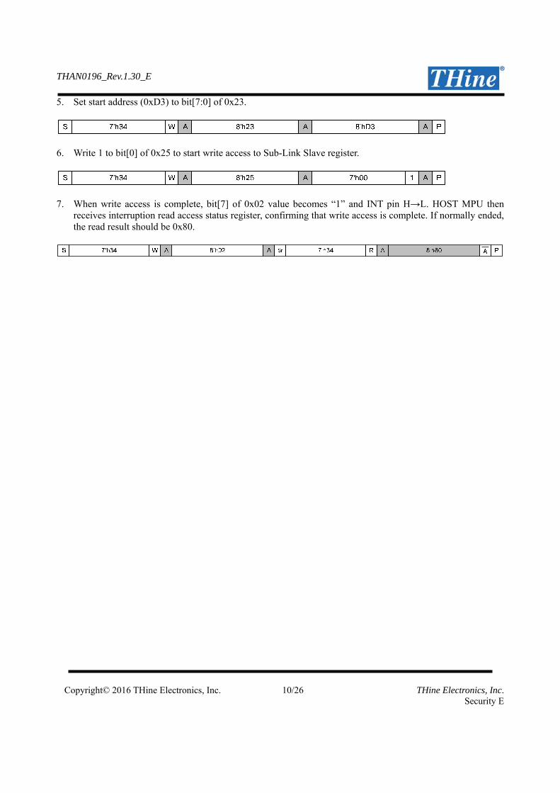
Copyright© 2016 THine Electronics, Inc. 10/26 THine Electronics, Inc. Security E
5. Set start address (0xD3) to bit[7:0] of 0x23.
6. Write 1 to bit[0] of 0x25 to start write access to Sub-Link Slave register.
7. When write access is complete, bit[7] of 0x02 value becomes “1” and INT pin H→L. HOST MPU then
receives interruption read access status register, confirming that write access is complete. If normally ended, the read result should be 0x80.
THAN0196_Rev.1.30_E
Copyright© 2016 THine Electronics, Inc. 11/26 THine Electronics, Inc. Security E
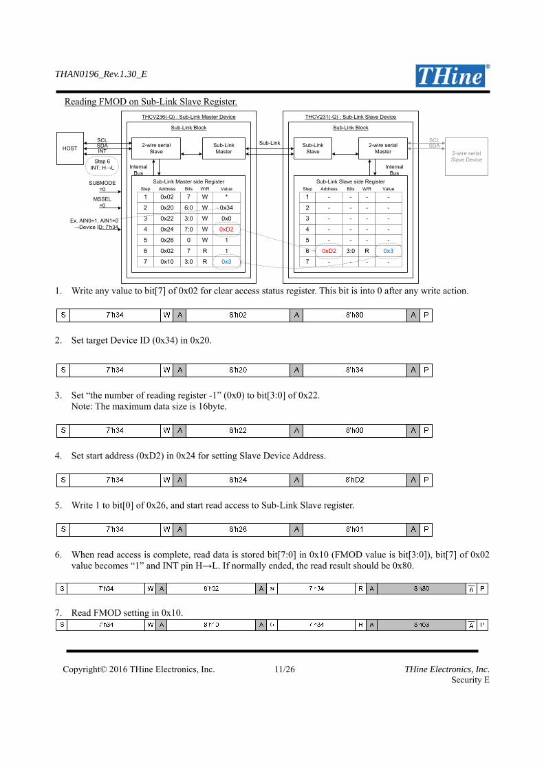
Reading FMOD on Sub-Link Slave Register.
Sub-Link Block
2-wire serial Slave
HOST
SCLSDA
Sub-Link Master side Register
Sub-LinkMaster
THCV236(-Q) : Sub-Link Master Device THCV231(-Q) : Sub-Link Slave Device
Sub-Link Block
Sub-LinkSlave
2-wire serial Master
Sub-Link
Internal Bus
Address
0x02
0x26
0x24
*
0x22
0x20
Bits Value
7
W/R
W
Step
1
0x346:0 W
0x03:0 W
5
4
3
2
0xD27:0 W
10 W
0x026 17 R
INT
Sub-Link Slave side Register
Internal Bus
Address
0xD2 0x3
Bits Value
3:0
W/R
R
Step
Step 6INT: H→L
SCLSDA
1
5
4
3
2
6
- -- -
- -- -
- -- -
- -- -
- -- -
0x107 0x33:0 R 7 - -- -
MSSEL=0
SUBMODE=0
Ex. AIN0=1, AIN1=0→Device ID: 7'h34
2-wire serial Slave Device
1. Write any value to bit[7] of 0x02 for clear access status register. This bit is into 0 after any write action.
2. Set target Device ID (0x34) in 0x20.
3. Set “the number of reading register -1” (0x0) to bit[3:0] of 0x22. Note: The maximum data size is 16byte.
4. Set start address (0xD2) in 0x24 for setting Slave Device Address.
5. Write 1 to bit[0] of 0x26, and start read access to Sub-Link Slave register.
6. When read access is complete, read data is stored bit[7:0] in 0x10 (FMOD value is bit[3:0]), bit[7] of 0x02 value becomes “1” and INT pin H→L. If normally ended, the read result should be 0x80.
7. Read FMOD setting in 0x10.
THAN0196_Rev.1.30_E
Copyright© 2016 THine Electronics, Inc. 12/26 THine Electronics, Inc. Security E
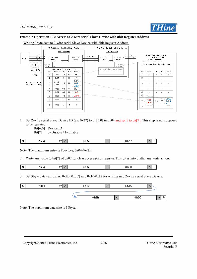
Example Operation 1-3: Access to 2-wire serial Slave Device with 8bit Register Address
Writing 3byte data to 2-wire serial Slave Device with 8bit Register Address.
1. Set 2-wire serial Slave Device ID (ex. 0x27) to bit[6:0] in 0x04 and set 1 to bit[7]. This step is not supposed
to be repeated. Bit[6:0] Device ID Bit[7] 0=Disable / 1=Enable
Note: The maximum entry is 8devices, 0x04-0x0B. 2. Write any value to bit[7] of 0x02 for clear access status register. This bit is into 0 after any write action.
3. Set 3byte data (ex. 0x1A, 0x2B, 0x3C) into 0x10-0x12 for writing into 2-wire serial Slave Device.
Note: The maximum data size is 16byte.
THAN0196_Rev.1.30_E
Copyright© 2016 THine Electronics, Inc. 13/26 THine Electronics, Inc. Security E
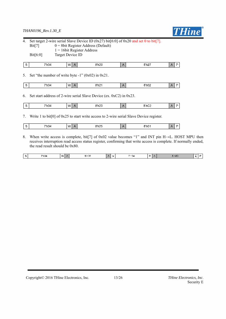
4. Set target 2-wire serial Slave Device ID (0x27) bit[6:0] of 0x20 and set 0 to bit[7]. Bit[7] 0 = 8bit Register Address (Default)
1 = 16bit Register Address Bit[6:0] Target Device ID
5. Set “the number of write byte -1” (0x02) in 0x21.
6. Set start address of 2-wire serial Slave Device (ex. 0xC2) in 0x23.
7. Write 1 to bit[0] of 0x25 to start write access to 2-wire serial Slave Device register.
8. When write access is complete, bit[7] of 0x02 value becomes “1” and INT pin H→L. HOST MPU then
receives interruption read access status register, confirming that write access is complete. If normally ended, the read result should be 0x80.
THAN0196_Rev.1.30_E
Copyright© 2016 THine Electronics, Inc. 14/26 THine Electronics, Inc. Security E
Example Operation 1-4: Access to 2-wire serial Slave Device with 16bit Register Address
Reading 3byte data to 2-wire serial Slave Device with 16bit Register Address.
1
Sub-Link Block
2-wire serial Slave
HOST
SCLSDA
Sub-Link Master side Register
Sub-LinkMaster
THCV236(-Q) : Sub-Link Master Device THCV231(-Q) : Sub-Link Slave Device
Sub-Link Block
Sub-LinkSlave
2-wire serial Master
Sub-Link
Internal Bus
Address
0x04
0x02
0x29
0x22
0xBB
0x20
Bits Value
7:0
W/R
W
Step
1
*7 W
0xBB7:0 W
5-1
4
2
5-2
0x23:0 W
0xA27:0 W
0x2A
6
0x5D7:0 W
INT
Sub-Link Slave side Register
Internal Bus
Address Bits ValueW/RStep
Step 8INT: H→L
SCLSDA
1
5
4
3
2
6
- -- -
- -- -
- -- -
- -- -
- -- -
- -- -
2-wire serial Slave DeviceEx. device ID: 7'h3B
Register Address: 16bit
2-wire serial Slave Device Register
MSSEL=0
0x027 17 R 7 0x5DA2-0x5DA4
7:0 R0xA1, 0x92, 0x83
3
0x2C 0 W
0xA1, 0x92, 0x83
0x10-0x12
7:0 R8 -- - -8
SUBMODE=0
Ex. AIN0=1, AIN1=0→Device ID: 7'h34
1. Set 2-wire serial Slave Device ID (ex. 0x3B) to bit[6:0] of 0x04 and set 1 to bit[7]. This step is not supposed
to be repeated. Bit[7] 0=Disable (Default) / 1=Enable Bit[6:0] Device ID
Note: The maximum entry is 8devices, 0x04-0x0B.
2. Write any value to bit[7] of 0x02 for clear access status register. This bit is into 0 after any write action.
3. Set target 2-wire serial Slave Device ID (0x3B) bit[6:0] of 0x20 for reading register access and set 1 to
bit[7] for 16bit Register Address. Bit[7] 0 = 8bit Register Address (Default)
1 = 16bit Register Address Bit[6:0] Target Device ID
THAN0196_Rev.1.30_E
Copyright© 2016 THine Electronics, Inc. 15/26 THine Electronics, Inc. Security E
4. Set “the number of read byte -1” (0x02) in 0x22. Note: The maximum data size is 16byte.
5. Set start address of 2-wire serial Slave Device ID (ex. 0x5DA2) in 0x29 and 0x2A. 0x29: start address [7:0] 0x2A: start address [15:8]
S 8'h297'h34 W A A 8'hA2 A 8'h5D A P
6. Write 1 to bit[0] of 0x2C to start read access to 2-wire serial Slave Device register.
7. When read access is complete, reading data is stored into 0x10-0x12, bit[7] of 0x02 becomes “1”, and INT
pin H→L. If normally ended, the read result should be 0x80.
8. Read 3 byte data in 0x10-0x12.
S 8'h107'h34 W A A
A P
7'h34 R
A
Sr
8'hA1 A 8'h92 A 8'h83
THAN0196_Rev.1.30_E
Copyright© 2016 THine Electronics, Inc. 16/26 THine Electronics, Inc. Security E
Example Operation 2-1: Through GPIO Sub-Link Master to Sub-Link Slave
Control through GPIO of the THCV236(-Q) (Sub-Link Master) and through GPIO of the THCV231(-Q)
(Sub-Link Slave Device).
1. GPIO transmission type setting with bit[4:3] of 0x40 (Master side Register) and bit[4:3] of 0xC0 (Slave side
Register, refer to page 9). 0 = Programmable GPIO enable 1 = Through GPIO enable (Default)
2. GPIO output buffer type setting with bit[4:3] of 0xC6 (Slave side Register). 1=Push-pull output 0=Open-Drain output (Default)
3. GPIO polarity setting with bit[4:3] of 0x43 (Master side Register) and bit[4:3] of 0xC3 (Slave side
Register). 1=Input 0=Output
4. GPIO4 and GPIO3 input of Master side is updated automatically to GPIO4 and GPIO3 output of Slave side. Note: This through GPIO function is able to use with default register setting.
THAN0196_Rev.1.30_E
Copyright© 2016 THine Electronics, Inc. 17/26 THine Electronics, Inc. Security E
Example Operation 2-2: Programmable GPIO output control
Control output GPIO of the THCV236(-Q) (Sub-Link Master side) and GPIO of the THCV231(-Q)
(Sub-Link Slave side).
Sub-Link Block
2-wire serial Slave
HOST
SCLSDA
Sub-Link Master side Register
Sub-LinkMaster
THCV236(-Q) : Sub-Link Master Device THCV231(-Q) : Sub-Link Slave Device
Sub-Link Block
Sub-LinkSlave
2-wire serial Master
Sub-Link
Internal Bus
Address
0x40
0x46
0x0
0x43
0x42
Bits Value
4:3W/R
WStep
1
Valid4:3 W
Valid4:3 W
0x04:3 W4
3
2
INT
Sub-Link Slave side Register
Internal Bus
Address Bits ValueW/RStep
SCLSDA
1
4
3
2
0xC0 0x04:3 W
0xC6 Valid4:3 W
0xC2 Valid4:3 W
0xC3 0x04:3 W
MSSEL=0
GPIO4, GPIO3 = H / L GPIO4, GPIO3 = H / L
SUBMODE=0
AIN1, AIN0=00:7'h0B01:7'h3410:7'h7711:7'h65
2-wire serial Slave Device
1. GPIO transmission type setting with bit[4:3] of 0x40 (Master side Register) and bit[4:3] of 0xC0 (Slave side
Register, refer to page9). 0 = Programmable GPIO enable 1 = Through GPIO enable (Default)
2. GPIO output buffer type setting with bit[4:3] of 0x46 (Master side Register) and bit[4:3] of 0xC6 (Slave side Register). 1=Push-pull output 0=Open-Drain output (Default)
3. GPIO output value setting with bit[4:3] of 0x42 (Master side Register) and bit[4:3] of 0xC2 (Slave side Register). 1=H (Push-pull output: H / Open-Drain output: Hi-Z) 0=L (Default)
4. GPIO polarity setting with bit[4:3] of 0x43 (Master side Register) and bit[4:3] of 0xC3 (Slave side Register). 1=Input 0=Output
THAN0196_Rev.1.30_E
Copyright© 2016 THine Electronics, Inc. 18/26 THine Electronics, Inc. Security E
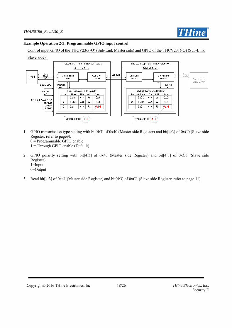
Example Operation 2-3: Programmable GPIO input control
Control input GPIO of the THCV236(-Q) (Sub-Link Master side) and GPIO of the THCV231(-Q) (Sub-Link
Slave side).
1. GPIO transmission type setting with bit[4:3] of 0x40 (Master side Register) and bit[4:3] of 0xC0 (Slave side
Register, refer to page9). 0 = Programmable GPIO enable 1 = Through GPIO enable (Default)
2. GPIO polarity setting with bit[4:3] of 0x43 (Master side Register) and bit[4:3] of 0xC3 (Slave side Register). 1=Input 0=Output
3. Read bit[4:3] of 0x41 (Master side Register) and bit[4:3] of 0xC1 (Slave side Register, refer to page 11).
THAN0196_Rev.1.30_E
Copyright© 2016 THine Electronics, Inc. 19/26 THine Electronics, Inc. Security E
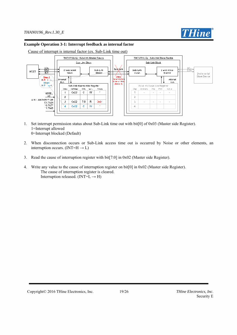
Example Operation 3-1: Interrupt feedback as internal factor
Cause of interrupt is internal factor (ex. Sub-Link time out)
1. Set interrupt permission status about Sub-Link time out with bit[0] of 0x03 (Master side Register).
1=Interrupt allowed 0=Interrupt blocked (Default)
2. When disconnection occurs or Sub-Link access time out is occurred by Noise or other elements, an interruption occurs. (INT=H → L)
3. Read the cause of interruption register with bit[7:0] in 0x02 (Master side Register). 4. Write any value to the cause of interruption register on bit[0] in 0x02 (Master side Register).
The cause of interruption register is cleared. Interruption released. (INT=L → H)
THAN0196_Rev.1.30_E
Copyright© 2016 THine Electronics, Inc. 20/26 THine Electronics, Inc. Security E
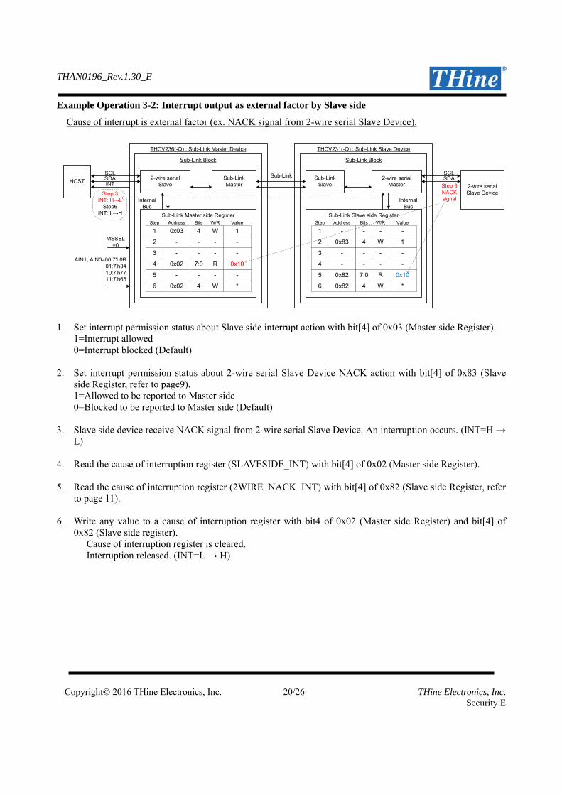
Example Operation 3-2: Interrupt output as external factor by Slave side
Cause of interrupt is external factor (ex. NACK signal from 2-wire serial Slave Device).
Sub-Link Block
2-wire serial Slave
HOST
SCLSDA
Sub-Link Master side Register
Sub-LinkMaster
THCV236(-Q) : Sub-Link Master Device THCV231(-Q) : Sub-Link Slave Device
Sub-Link Block
Sub-LinkSlave
2-wire serial Master
Sub-Link
Internal Bus
Address
0x83
-
1
Bits Value
4
W/R
W
Step
1
--3
2
INT
Sub-Link Slave side Register
Internal Bus
Address Bits ValueW/RStep
SCLSDA
1
3
2MSSEL
=0
0x03 14 W
-
- -- -
0x02 0x10R4 7:0
0x82 0x10R5 7:0
4
5
- -- -
- -- -
- -- -
Step 3INT: H→L
Step6INT: L→H
Step 3NACK signal
- -- -
0x82 *W6 460x02 *4 W
AIN1, AIN0=00:7'h0B01:7'h3410:7'h7711:7'h65
2-wire serial Slave Device
1. Set interrupt permission status about Slave side interrupt action with bit[4] of 0x03 (Master side Register).
1=Interrupt allowed 0=Interrupt blocked (Default)
2. Set interrupt permission status about 2-wire serial Slave Device NACK action with bit[4] of 0x83 (Slave side Register, refer to page9). 1=Allowed to be reported to Master side 0=Blocked to be reported to Master side (Default)
3. Slave side device receive NACK signal from 2-wire serial Slave Device. An interruption occurs. (INT=H →
L) 4. Read the cause of interruption register (SLAVESIDE_INT) with bit[4] of 0x02 (Master side Register). 5. Read the cause of interruption register (2WIRE_NACK_INT) with bit[4] of 0x82 (Slave side Register, refer
to page 11).
6. Write any value to a cause of interruption register with bit4 of 0x02 (Master side Register) and bit[4] of 0x82 (Slave side register).
Cause of interruption register is cleared. Interruption released. (INT=L → H)
THAN0196_Rev.1.30_E
Copyright© 2016 THine Electronics, Inc. 21/26 THine Electronics, Inc. Security E
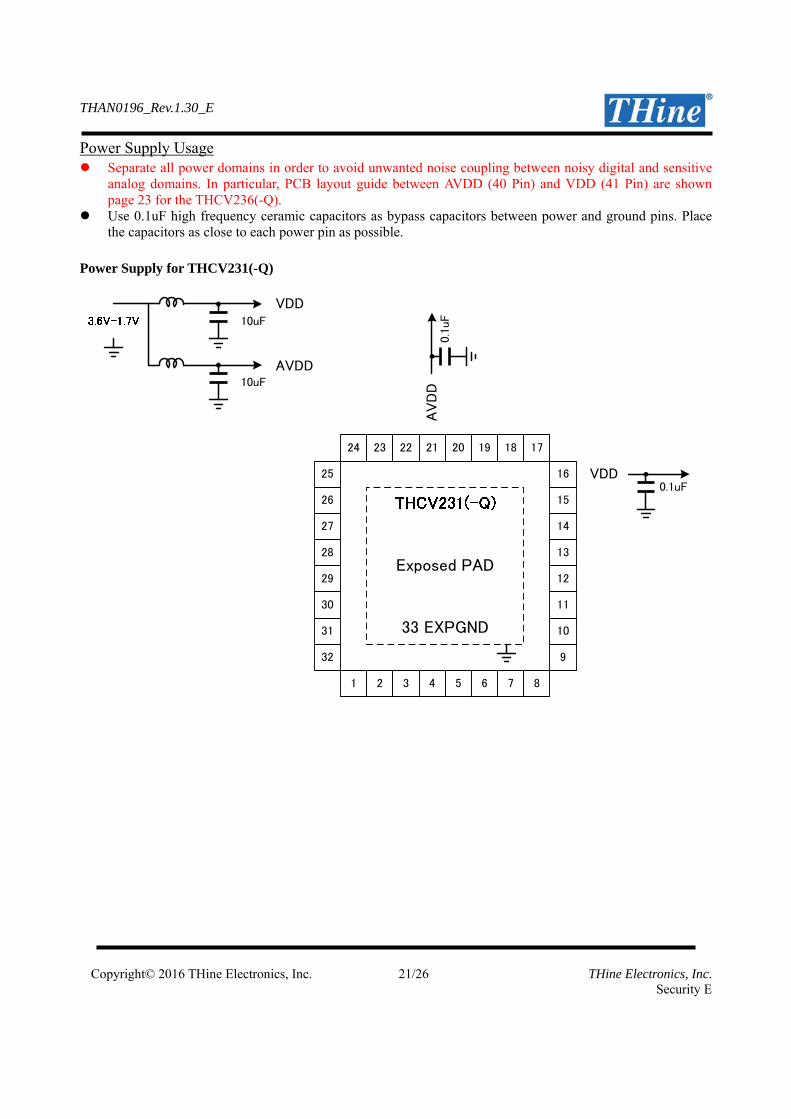
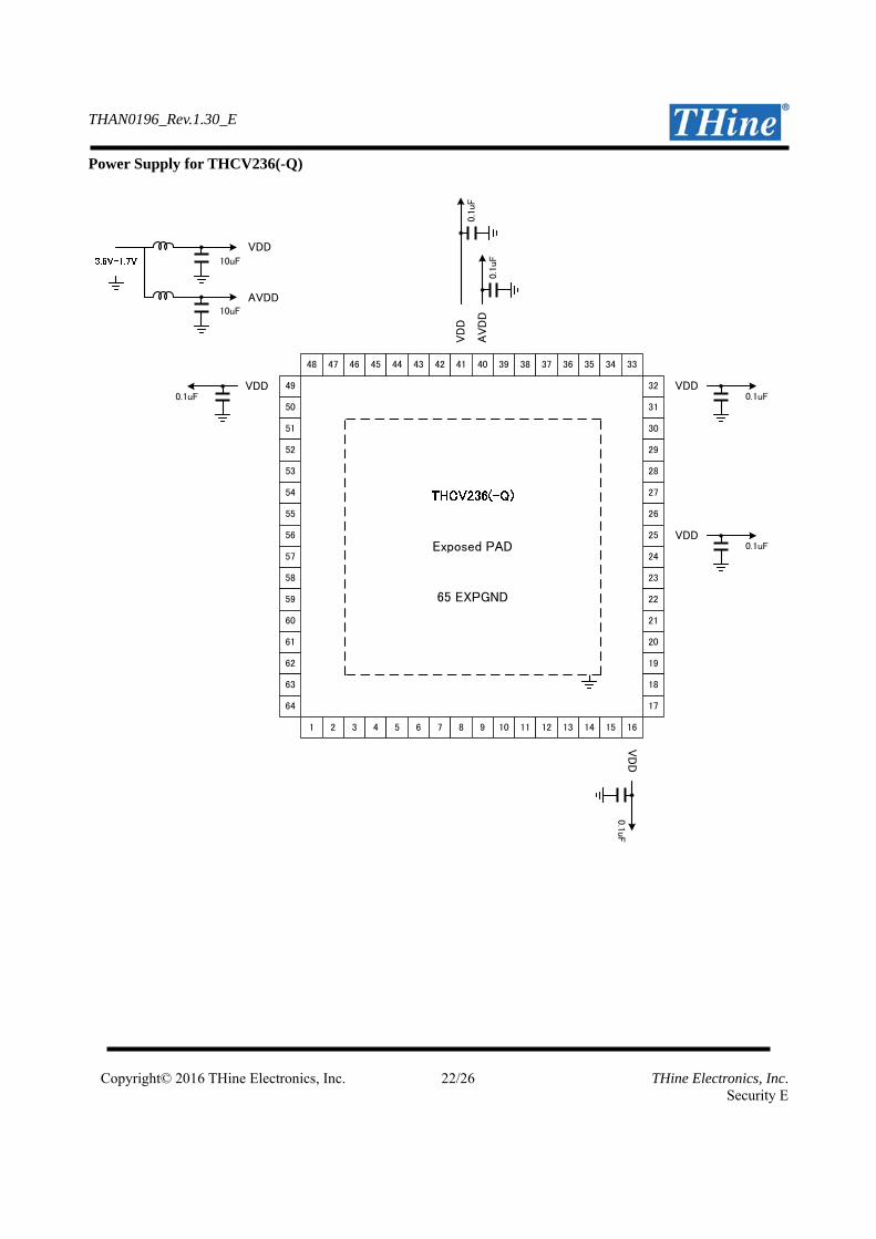
Power Supply Usage Separate all power domains in order to avoid unwanted noise coupling between noisy digital and sensitive
analog domains. In particular, PCB layout guide between AVDD (40 Pin) and VDD (41 Pin) are shown page 23 for the THCV236(-Q).
Use 0.1uF high frequency ceramic capacitors as bypass capacitors between power and ground pins. Place the capacitors as close to each power pin as possible.
Power Supply for THCV231(-Q)
25
26
27
28
29
30
31
32
1 2 3 4 5 6 7 8
16
15
14
13
12
11
10
9
24 23 22 21 20 19 18 17
Exposed PAD
33 EXPGND
VDD
AV
DD
10uF
10uF
0.1
uF
0.1uF
AVDD
VDD
THAN0196_Rev.1.30_E
Copyright© 2016 THine Electronics, Inc. 22/26 THine Electronics, Inc. Security E
Power Supply for THCV236(-Q)
49
50
51
52
53
54
55
56
1 2 3 4 5 6 7 8
48 47 46 45 44 43 42 41
VDD
AV
DD
10uF
10uF
0.1
uF
0.1uF
AVDD
VDD
57
58
59
60
61
62
63
64
9 10 11 12 13 14 15 16
32
31
30
29
28
27
26
25
24
23
22
21
20
19
18
17
40 39 38 37 36 35 34 33
VD
D0.1
uF
VD
D0.1
uF
VDD0.1uF
VDD0.1uFExposed PAD
65 EXPGND
THAN0196_Rev.1.30_E
Copyright© 2016 THine Electronics, Inc. 23/26 THine Electronics, Inc. Security E
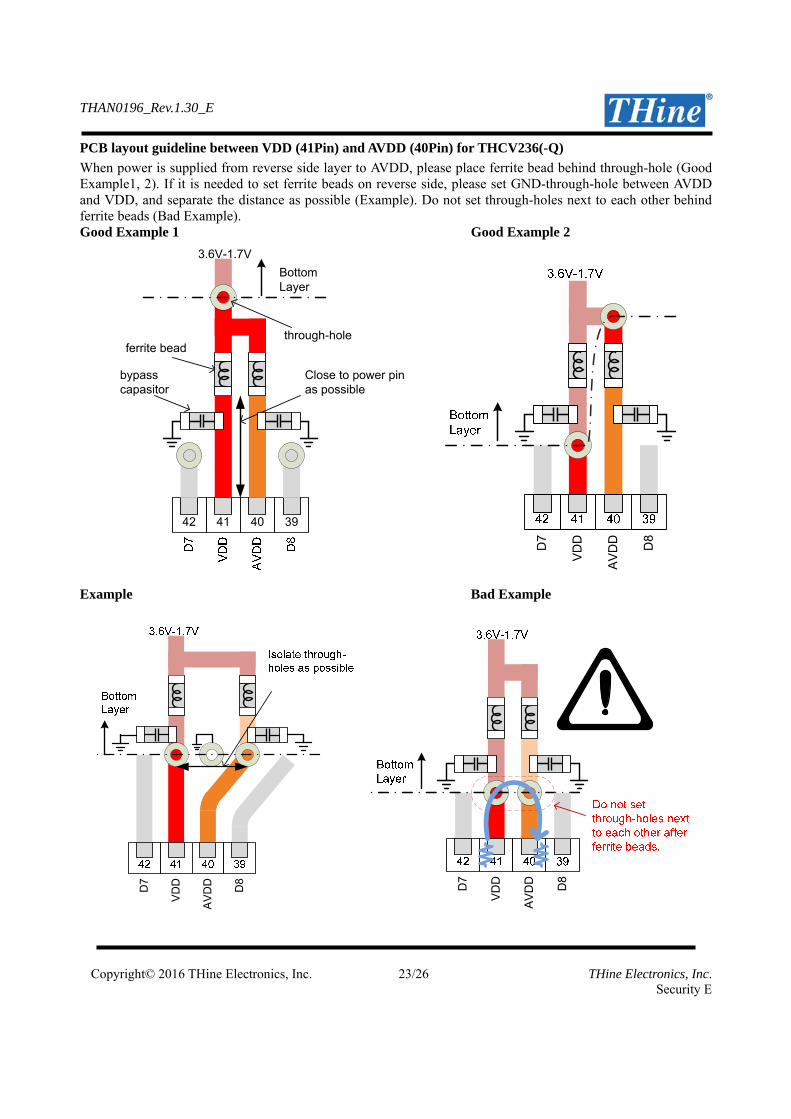
PCB layout guideline between VDD (41Pin) and AVDD (40Pin) for THCV236(-Q)
When power is supplied from reverse side layer to AVDD, please place ferrite bead behind through-hole (Good Example1, 2). If it is needed to set ferrite beads on reverse side, please set GND-through-hole between AVDD and VDD, and separate the distance as possible (Example). Do not set through-holes next to each other behind ferrite beads (Bad Example). Good Example 1 Good Example 2
41 40
BottomLayer
3942
3.6V-1.7V
ferrite bead
bypass capasitor
through-hole
Close to power pin as possible
AV
DD
VD
DD7
D8
Example Bad Example
AV
DD
VD
DD7
D8
AV
DD
VD
D
D7
D8
THAN0196_Rev.1.30_E
Copyright© 2016 THine Electronics, Inc. 24/26 THine Electronics, Inc. Security E
Note
1) Power On Sequence Do not input clock or data before the THCV231(-Q) on in order to keep absolute maximum ratings.
2) Cable Connection and Disconnection
Do not connect and disconnect the LVCMOS and CML cable/connector, when the power is supplied to the system.
3) GND Connection Connect the each GND of the PCB where the THCV231(-Q) and THCV236(-Q) are on it. It is better for EMI reduction to place GND cable as close to LVCMOS and CML cable as possible.
4) Low Input Pulse into PDN, PDN1 and PDN0 Period Requirement
Do not input Low Pulse within 1msec into PDN (THCV231(-Q)), PDN1 and PDN0 (THCV236(-Q)).
THAN0196_Rev.1.30_E
Copyright© 2016 THine Electronics, Inc. 25/26 THine Electronics, Inc. Security E
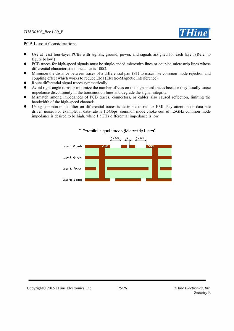
PCB Layout Considerations Use at least four-layer PCBs with signals, ground, power, and signals assigned for each layer. (Refer to
figure below.) PCB traces for high-speed signals must be single-ended microstirp lines or coupled microstrip lines whose
differential characteristic impedance is 100Ω. Minimize the distance between traces of a differential pair (S1) to maximize common mode rejection and
coupling effect which works to reduce EMI (Electro-Magnetic Interference). Route differential signal traces symmetrically. Avoid right-angle turns or minimize the number of vias on the high speed traces because they usually cause
impedance discontinuity in the transmission lines and degrade the signal integrity. Mismatch among impedances of PCB traces, connectors, or cables also caused reflection, limiting the
bandwidth of the high-speed channels. Using common-mode filter on differential traces is desirable to reduce EMI. Pay attention on data-rate
driven noise. For example, if data-rate is 1.5Gbps, common mode choke coil of 1.5GHz common mode impedance is desired to be high, while 1.5GHz differential impedance is low.
THAN0196_Rev.1.30_E
Copyright© 2016 THine Electronics, Inc. 26/26 THine Electronics, Inc. Security E
Notices and Requests 1. The product specifications described in this material are subject to change without prior notice. 2. The circuit diagrams described in this material are examples of the application which may not always apply
to the customer's design. We are not responsible for possible errors and omissions in this material. Please note if errors or omissions should be found in this material, we may not be able to correct them immediately.
3. This material contains our copyright, know-how or other proprietary. Copying or disclosing to third parties the contents of this material without our prior permission is prohibited.
4. Note that if infringement of any third party's industrial ownership should occur by using this product, we will be exempted from the responsibility unless it directly relates to the production process or functions of the product.
5. Product Application 5.1. Application of this product is intended for and limited to the following applications:
audio-video device, office automation device, communication device, consumer electronics, smartphone, feature phone, and amusement machine device. This product must not be used for applications that require extremely high-reliability/safety such as aerospace device, traffic device, transportation device, nuclear power control device, combustion chamber device, medical device related to critical care, or any kind of safety device.
5.2. This product is not intended to be used as an automotive part, unless the product is specified as a product conforming to the demands and specifications of ISO/TS16949 ("the Specified Product") in this data sheet. THine Electronics, Inc. (“THine”) accepts no liability whatsoever for any product other than the Specified Product for it not conforming to the aforementioned demands and specifications.
5.3. THine accepts liability for demands and specifications of the Specified Product only to the extent that the user and THine have been previously and explicitly agreed to each other.
6. Despite our utmost efforts to improve the quality and reliability of the product, faults will occur with a certain small probability, which is inevitable to a semi-conductor product. Therefore, you are encouraged to have sufficiently redundant or error preventive design applied to the use of the product so as not to have our product cause any social or public damage.
7. Please note that this product is not designed to be radiation-proof. 8. Testing and other quality control techniques are used to this product to the extent THine deems necessary
to support warranty for performance of this product. Except where mandated by applicable law or deemed necessary by THine based on the user’s request, testing of all functions and performance of the product is not necessarily performed.
9. Customers are asked, if required, to judge by themselves if this product falls under the category of strategic goods under the Foreign Exchange and Foreign Trade Control Law.
10. The product or peripheral parts may be damaged by a surge in voltage over the absolute maximum ratings or malfunction, if pins of the product are shorted by such as foreign substance. The damages may cause a smoking and ignition. Therefore, you are encouraged to implement safety measures by adding protection devices, such as fuses.
THine Electronics, Inc. [email protected]


![GP VD150 E Operating Instruction Eng Ger Fre Ita Spa Rus · 1 1 Press the [CAM1], [CAM2], [CAM3] or [CAM4] button to select the unit. 2 Press the [MENU] button for at least 2 seconds](https://img.pdfslide.net/doc/110x75/5f053f5c7e708231d41203e2/gp-vd150-e-operating-instruction-eng-ger-fre-ita-spa-rus-1-1-press-the-cam1-cam2.jpg)