Embed Size (px)
Citation preview
General rights Copyright and moral rights for the publications made accessible in the public portal are retained by the authors and/or other copyright owners and it is a condition of accessing publications that users recognise and abide by the legal requirements associated with these rights.
Users may download and print one copy of any publication from the public portal for the purpose of private study or research.
You may not further distribute the material or use it for any profit-making activity or commercial gain
You may freely distribute the URL identifying the publication in the public portal If you believe that this document breaches copyright please contact us providing details, and we will remove access to the work immediately and investigate your claim.
Downloaded from orbit.dtu.dk on: Apr 21, 2020
The Analysis and Comparison of Leakage Inductance in Different WindingArrangements for Planar Transformer
Ouyang, Ziwei; Thomsen, Ole Cornelius; Andersen, Michael Andreas E.
Published in:International Conference on Power Electronics and Drive Systems, 2009. PEDS 2009
Link to article, DOI:10.1109/PEDS.2009.5385844
Publication date:2009
Document VersionPublisher's PDF, also known as Version of record
Link back to DTU Orbit
Citation (APA):Ouyang, Z., Thomsen, O. C., & Andersen, M. A. E. (2009). The Analysis and Comparison of LeakageInductance in Different Winding Arrangements for Planar Transformer. In International Conference on PowerElectronics and Drive Systems, 2009. PEDS 2009 (pp. 1143-1148). IEEE.https://doi.org/10.1109/PEDS.2009.5385844
The Analysis and Comparison of Leakage Inductance in Different Winding Arrangements for Planar Transformer
Ziwei Ouyang, Ole C. Thomsen, Michael A. E. Andersen
Department of Electrical Engineering, Technical University of Denmark
Kgs. Lyngby, 2800, Denmark [email protected]
Abstract -- The coupling of the windings can be easily
increased by using multiply stacked planar windings connection. Interleaving is a well-known technique used to reduce leakage inductance and minimize high-frequency winding losses. The paper aims to analyze leakage inductance based on magneto motive force (MMF) and energy distribution in planar transformer and correct the formula of leakage inductance proposed by previous publications. The investigation of different winding arrangements shows significant advantages of interleaving structure. In this work, a novel half turn structure is proposed to reduce leakage inductance further. Some important issues are presented to acquire desired leakage inductance. The design and modeling of 1 kW planar transformer is presented. In order to verify the analytical method for leakage inductance in this paper, finite element analysis (FEA) and measurement with impedance analyzer are presented. Good matching between calculation, FEA 2D simulation and measurement results is achieved.
Index Terms-- leakage inductance, magneto motive force (MMF), finite element analysis (FEA), interleaving, half turn, planar transformer
I. INTRODUCTION In recent years, planar transformers have become
increasingly popular in high frequency power converter design because of the advantages they achieved in terms of increased reliability, reproducibility, and increased power density. In terms of circuit performance one of the advantages of planar transformer is low profile and repeatable leakage inductance [1]. The leakage inductance causes the main switch current at the device input to vary at a low slope between zero and rated value and reduces the rate of commutation between output diodes. In addition, the stored energy in the leakage inductance leads to the generation of voltage spikes on the main switch which, besides creating EMI problems, increases the switching losses and lowers the efficiency [2]. Therefore, most designers expect the leakage inductance to be as small as possible. However, in some applications such as a phase-shift-modulated soft switching DC/DC converter, the magnitude of the leakage inductance determines the achievable load range under zero-voltage operation, and a relatively large leakage inductance is desirable. This paper aims to calculate the leakage inductance stored in planar transformer by analyzing magneto motive force (MMF) and energy distribution. Section ІІ defines leakage inductance using the perspective of energy. The energy associated with leakage inductance should be equal to
the sum of energy stored in each element layer inside the core window. The section also analyzes the magnetic field strength in each layer and finite element analysis 2D model is simulated to demonstrate the correctness of the analytical method. As presented in previous publications [3-5], the formula (see eqn.6) is generally used to calculate the leakage inductance. However, it must be noted that the formula doesn’t provide precise results. It assumes that the magnetic field strength along the height of insulator layer between non-interleaved sections varies linearly but actually it should keep constant during the whole area of insulator layer. In order to correct the previous formula, a new formula suited for symmetrical winding arrangement is proposed in this paper. The error analysis on the two calculations is also presented. Section ІІІ proposes a novel half turn structure to reduce leakage inductance further. The MMF distribution curve for half turn arrangement is analyzed and leakage inductance is computed. Section ІV describes some important issues to require desired leakage inductance including copper thickness, the thickness of insulator layer and the number of turns. Section V evaluates the good matching between calculation, FEA 2D simulation and measurement with impedance analyzer (PSM1735+ Impedance Analysis Interface and Kelvin Fixture) which indicates the correctness of the analytical method and the proposed calculation. Section V provides the conclusion.
II. BASIC DEFINITION AND CALCULATION FOR LEAKAGE INDUCTANCE
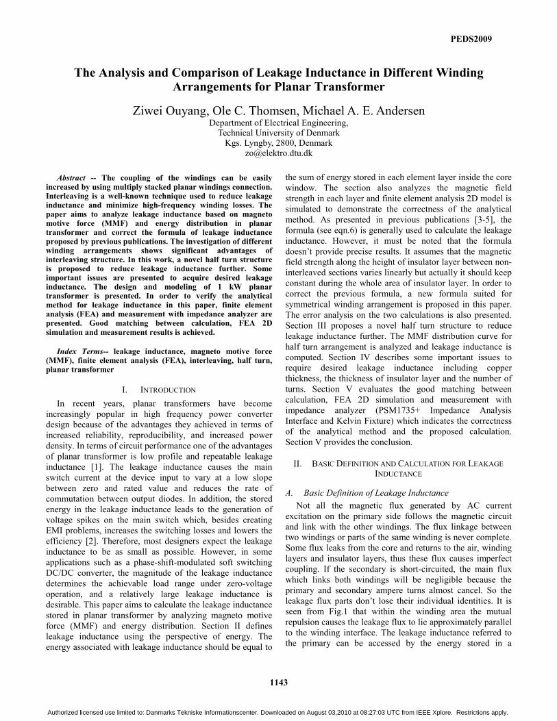
A. Basic Definition of Leakage Inductance Not all the magnetic flux generated by AC current
excitation on the primary side follows the magnetic circuit and link with the other windings. The flux linkage between two windings or parts of the same winding is never complete. Some flux leaks from the core and returns to the air, winding layers and insulator layers, thus these flux causes imperfect coupling. If the secondary is short-circuited, the main flux which links both windings will be negligible because the primary and secondary ampere turns almost cancel. So the leakage flux parts don’t lose their individual identities. It is seen from Fig.1 that within the winding area the mutual repulsion causes the leakage flux to lie approximately parallel to the winding interface. The leakage inductance referred to the primary can be accessed by the energy stored in a
PEDS2009
1143
Authorized licensed use limited to: Danmarks Tekniske Informationscenter. Downloaded on August 03,2010 at 08:27:03 UTC from IEEE Xplore. Restrictions apply.
magnetic field, 2
21
21
pIlkLtotal
dVHBenergyE ⋅⋅=∫ ⋅⋅= (1)
11IN×
٠
P
S 22IN
wb
xd
symmetry axis
MMF Distribution
Fig. 1 The leakage flux paths and magneto motive force variation (MMF)
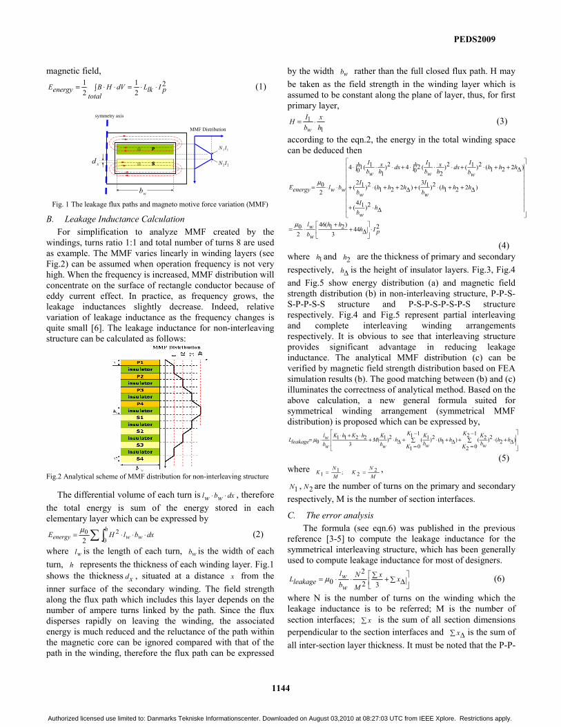
B. Leakage Inductance Calculation For simplification to analyze MMF created by the
windings, turns ratio 1:1 and total number of turns 8 are used as example. The MMF varies linearly in winding layers (see Fig.2) can be assumed when operation frequency is not very high. When the frequency is increased, MMF distribution will concentrate on the surface of rectangle conductor because of eddy current effect. In practice, as frequency grows, the leakage inductances slightly decrease. Indeed, relative variation of leakage inductance as the frequency changes is quite small [6]. The leakage inductance for non-interleaving structure can be calculated as follows:
Fig.2 Analytical scheme of MMF distribution for non-interleaving structure
The differential volume of each turn is dxwbwl ⋅⋅ , therefore the total energy is sum of the energy stored in each elementary layer which can be expressed by
∑∫ ⋅⋅⋅=h
wwenergy dxblHE0
202
μ (2)
where wl is the length of each turn, wb is the width of each turn, h represents the thickness of each winding layer. Fig.1 shows the thickness xd , situated at a distance x from the inner surface of the secondary winding. The field strength along the flux path which includes this layer depends on the number of ampere turns linked by the path. Since the flux disperses rapidly on leaving the winding, the associated energy is much reduced and the reluctance of the path within the magnetic core can be ignored compared with that of the path in the winding, therefore the flux path can be expressed
by the width wb rather than the full closed flux path. H may be taken as the field strength in the winding layer which is assumed to be constant along the plane of layer, thus, for first primary layer,
1
1hx
bIHw
⋅= (3)
according to the eqn.2, the energy in the total winding space can be deduced then
2443
)21(4620
2)14(
)221(2)13()221(2)12
(
10 20 )221(2)1(2)2
1(42)1
1(4
20
pIhhh
wbwl
hwbI
hhhwbI
hhhwbI
h h hhhwb
Idx
hx
wbI
dxhx
wbI
wbwlenergyE
⋅⎥⎦
⎤⎢⎣
⎡Δ+
+⋅=
⎥⎥⎥⎥⎥⎥⎥⎥
⎦
⎤
⎢⎢⎢⎢⎢⎢⎢⎢
⎣
⎡
Δ⋅+
Δ++⋅+Δ++⋅+
∫ ∫ Δ++⋅+⋅⋅⋅+⋅⋅⋅
⋅⋅=
μ
μ
(4) where 1h and 2h are the thickness of primary and secondary respectively, Δh is the height of insulator layers. Fig.3, Fig.4 and Fig.5 show energy distribution (a) and magnetic field strength distribution (b) in non-interleaving structure, P-P-S-S-P-P-S-S structure and P-S-P-S-P-S-P-S structure respectively. Fig.4 and Fig.5 represent partial interleaving and complete interleaving winding arrangements respectively. It is obvious to see that interleaving structure provides significant advantage in reducing leakage inductance. The analytical MMF distribution (c) can be verified by magnetic field strength distribution based on FEA simulation results (b). The good matching between (b) and (c) illuminates the correctness of analytical method. Based on the above calculation, a new general formula suited for symmetrical winding arrangement (symmetrical MMF distribution) is proposed which can be expressed by,
⎥⎥
⎦
⎤
⎢⎢
⎣
⎡∑
−
=Δ+⋅+∑
−
=Δ+⋅+Δ⋅+
⋅+⋅⋅=
12
02)2(2)2(
11
01)1(2)1(2)1(
32211
0K
Khh
wbKK
Khh
wbK
hwb
KM
hKhK
wbwl
leakageL μ
(5) where
MN
KMN
K 22;1
1 == ,
1N , 2N are the number of turns on the primary and secondary respectively, M is the number of section interfaces.
C. The error analysis The formula (see eqn.6) was published in the previous
reference [3-5] to compute the leakage inductance for the symmetrical interleaving structure, which has been generally used to compute leakage inductance for most of designers.
⎥⎦
⎤⎢⎣
⎡∑ Δ+∑⋅⋅= xx
M
N
wbwl
leakageL32
20μ (6)
where N is the number of turns on the winding which the leakage inductance is to be referred; M is the number of section interfaces; ∑ x is the sum of all section dimensions perpendicular to the section interfaces and ∑ Δx is the sum of all inter-section layer thickness. It must be noted that the P-P-
PEDS2009
1144
Authorized licensed use limited to: Danmarks Tekniske Informationscenter. Downloaded on August 03,2010 at 08:27:03 UTC from IEEE Xplore. Restrictions apply.
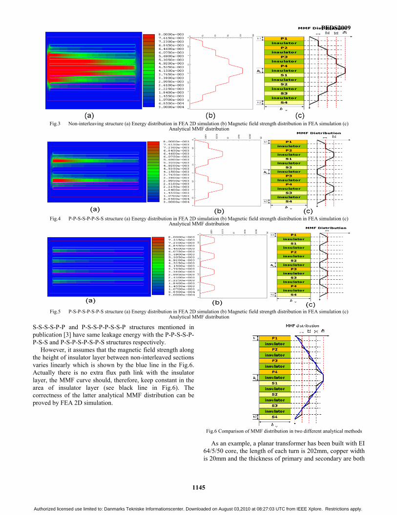
S-S-S-S-P-P and P-S-S-P-P-S-S-P structures mentioned in publication [3] have same leakage energy with the P-P-S-S-P-P-S-S and P-S-P-S-P-S-P-S structures respectively.
However, it assumes that the magnetic field strength along the height of insulator layer between non-interleaved sections varies linearly which is shown by the blue line in the Fig.6. Actually there is no extra flux path link with the insulator layer, the MMF curve should, therefore, keep constant in the area of insulator layer (see black line in Fig.6). The correctness of the latter analytical MMF distribution can be proved by FEA 2D simulation.
Fig.6 Comparison of MMF distribution in two different analytical methods
As an example, a planar transformer has been built with EI
64/5/50 core, the length of each turn is 202mm, copper width is 20mm and the thickness of primary and secondary are both
Fig.3 Non-interleaving structure (a) Energy distribution in FEA 2D simulation (b) Magnetic field strength distribution in FEA simulation (c)
Analytical MMF distribution
Fig.4 P-P-S-S-P-P-S-S structure (a) Energy distribution in FEA 2D simulation (b) Magnetic field strength distribution in FEA simulation (c)
Analytical MMF distribution
Fig.5 P-S-P-S-P-S-P-S structure (a) Energy distribution in FEA 2D simulation (b) Magnetic field strength distribution in FEA simulation (c)
Analytical MMF distribution
PEDS2009
1145
Authorized licensed use limited to: Danmarks Tekniske Informationscenter. Downloaded on August 03,2010 at 08:27:03 UTC from IEEE Xplore. Restrictions apply.
0.2mm, the thickness of insulator layer is 0.3mm. The winding arrangements P-P-P-P-S-S-S-S, P-P-S-S-P-P-S-S and P-S-P-S-P-S-P-S will be seen as case 1, case 2 and case 3 respectively. Table I describes the error between the proposed eqn.5 and the previous eqn.6.
TABLE I . THE ERROR ANALYSIS TABLE
Calculation (eqn.5) Previous Calculation (eqn.6) The error
Case 1 245 nH 291 nH 19%Case 2 62.6 nH 82.9 nH 32%Case 3 22 nH 25.8 nH 17%
III. NOVEL HALF TURN STRUCTURE The interleaving, partial interleaving and non-interleaving
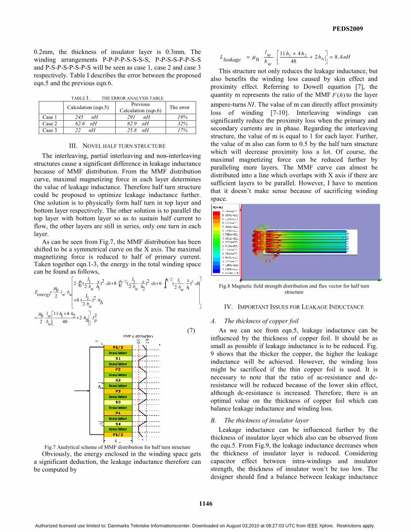
structures cause a significant difference in leakage inductance because of MMF distribution. From the MMF distribution curve, maximal magnetizing force in each layer determines the value of leakage inductance. Therefore half turn structure could be proposed to optimize leakage inductance further. One solution is to physically form half turn in top layer and bottom layer respectively. The other solution is to parallel the top layer with bottom layer so as to sustain half current to flow, the other layers are still in series, only one turn in each layer.
As can be seen from Fig.7, the MMF distribution has been shifted to be a symmetrical curve on the X axis. The maximal magnetizing force is reduced to half of primary current. Taken together eqn.1-3, the energy in the total winding space can be found as follows,
2248
24111
20
2)2
1(8
0 0 )2
(62)22
1(82)12
1(2
20
1 2 1
0
2
1
12/ 2/
pIhhh
wbwl
hwb
I
dxhx
wbIdxh
xwb
Idxh
xwb
I
wbwlenergyE
h h h
⋅⎥⎥⎦
⎤
⎢⎢⎣
⎡Δ⋅+
⋅+⋅⋅=
⎥⎥⎥⎥⎥
⎦
⎤
⎢⎢⎢⎢⎢
⎣
⎡
Δ⋅⋅
⋅+
∫ ∫ ⋅⋅⋅
⋅+⋅⋅⋅⋅+⋅⋅⋅⋅
⋅⋅=∫
μ
μ
(7)
Fig.7 Analytical scheme of MMF distribution for half turn structure
Obviously, the energy enclosed in the winding space gets a significant deduction, the leakage inductance therefore can be computed by
nHhhh
wbwl
leakageL 4.8248
4110
21 =⎥⎦⎤
⎢⎣⎡ ++⋅⋅= Δμ
This structure not only reduces the leakage inductance, but also benefits the winding loss caused by skin effect and proximity effect. Referring to Dowell equation [7], the quantity m represents the ratio of the MMF )(hF to the layer ampere-turns NI. The value of m can directly affect proximity loss of winding [7-10]. Interleaving windings can significantly reduce the proximity loss when the primary and secondary currents are in phase. Regarding the interleaving structure, the value of m is equal to 1 for each layer. Further, the value of m also can form to 0.5 by the half turn structure which will decrease proximity loss a lot. Of course, the maximal magnetizing force can be reduced further by paralleling more layers. The MMF curve can almost be distributed into a line which overlaps with X axis if there are sufficient layers to be parallel. However, I have to mention that it doesn’t make sense because of sacrificing winding space.
Fig.8 Magnetic field strength distribution and flux vector for half turn
structure
IV. IMPORTANT ISSUES FOR LEAKAGE INDUCTANCE
A. The thickness of copper foil As we can see from eqn.5, leakage inductance can be
influenced by the thickness of copper foil. It should be as small as possible if leakage inductance is to be reduced. Fig. 9 shows that the thicker the copper, the higher the leakage inductance will be achieved. However, the winding loss might be sacrificed if the thin copper foil is used. It is necessary to note that the ratio of ac-resistance and dc-resistance will be reduced because of the lower skin effect, although dc-resistance is increased. Therefore, there is an optimal value on the thickness of copper foil which can balance leakage inductance and winding loss.
B. The thickness of insulator layer Leakage inductance can be influenced further by the
thickness of insulator layer which also can be observed from the equ.5. From Fig.9, the leakage inductance decreases when the thickness of insulator layer is reduced. Considering capacitor effect between intra-windings and insulator strength, the thickness of insulator won’t be too low. The designer should find a balance between leakage inductance
PEDS2009
1146
Authorized licensed use limited to: Danmarks Tekniske Informationscenter. Downloaded on August 03,2010 at 08:27:03 UTC from IEEE Xplore. Restrictions apply.
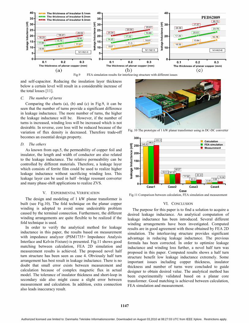
and self-capacitor. Reducing the insulation layer thickness below a certain level will result in a considerable increase of the total losses [11].
C. The number of turns Comparing the charts (a), (b) and (c) in Fig.9, it can be
seen that the number of turns provide a significant difference in leakage inductance. The more number of turns, the higher the leakage inductance will be. However, if the number of turns is increased, winding loss will be increased which is not desirable. In reverse, core loss will be reduced because of the variation of flux density is decreased. Therefore trade-off becomes an essential design property.
D. The others As known from eqn.5, the permeability of copper foil and
insulator, the length and width of conductor are also related to the leakage inductance. The relative permeability can be controlled by different materials. Therefore, a leakage layer which consists of ferrite film could be used to realize higher leakage inductance without sacrificing winding loss. This leakage layer can be used in half –bridge resonant converter and many phase-shift applications to realize ZVS.
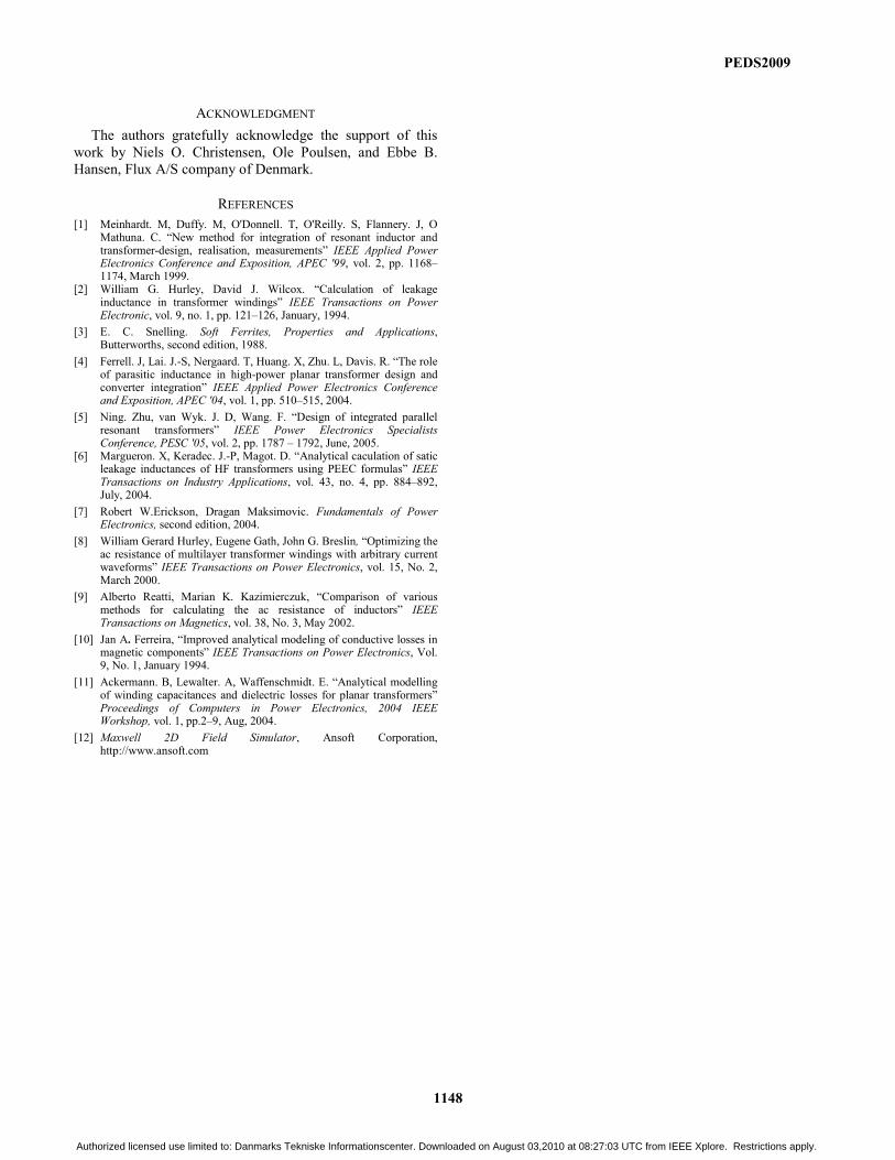
V. EXPERIMENTAL VERIFICATION The design and modeling of 1 kW planar transformer is
built (see Fig.10). The fold technique on the planar copper winding is adopted to avoid some undesirable problem caused by the terminal connection. Furthermore, the different winding arrangements are quite flexible to be realized if the fold technique is used.
In order to verify the analytical method for leakage inductance in this paper, the results based on measurement with impedance analyzer (PSM1735+ Impedance Analysis Interface and Kelvin Fixture) is presented. Fig.11 shows good matching between calculation, FEA 2D simulation and measurement results is achieved. The proposed novel half turn structure has been seen as case 4. Obviously half turn arrangement has best result in leakage inductance. There is no doubt that small error exists between measurement and calculation because of complex magnetic flux in actual model. The tolerance of insulator thickness and short-loop in secondary side also might cause a slight error between measurement and calculation. In addition, extra connection also leads inaccuracy result.
Fig. 10 The prototype of 1 kW planar transformer using in DC-DC converter
Fig.11 Comparison between calculation, FEA simulation and measurement
VI. CONCLUSION The purpose for this paper is to find a solution to acquire a
desired leakage inductance. An analytical computation of leakage inductance has been introduced. Several different winding arrangements have been investigated. Computed results are in good agreement with those obtained by FEA 2D simulation. The interleaving structure provides significant advantage in reducing leakage inductance. The previous formula has been corrected. In order to optimize leakage inductance and winding loss further, a novel half turn was proposed in this paper. Computed results shows a half turn structure benefit low leakage inductance extremely. Some important issues including copper thickness, insulator thickness and number of turns were concluded to guide designer to obtain desired value. The analytical method has been experimentally validated based on a planar core transformer. Good matching is achieved between calculation, FEA simulation and measurement.
Fig.9 FEA simulation results for interleaving structure with different issues
PEDS2009
1147
Authorized licensed use limited to: Danmarks Tekniske Informationscenter. Downloaded on August 03,2010 at 08:27:03 UTC from IEEE Xplore. Restrictions apply.
ACKNOWLEDGMENT The authors gratefully acknowledge the support of this
work by Niels O. Christensen, Ole Poulsen, and Ebbe B. Hansen, Flux A/S company of Denmark.
REFERENCES [1] Meinhardt. M, Duffy. M, O'Donnell. T, O'Reilly. S, Flannery. J, O
Mathuna. C. “New method for integration of resonant inductor and transformer-design, realisation, measurements” IEEE Applied Power Electronics Conference and Exposition, APEC '99, vol. 2, pp. 1168–1174, March 1999.
[2] William G. Hurley, David J. Wilcox. “Calculation of leakage inductance in transformer windings” IEEE Transactions on Power Electronic, vol. 9, no. 1, pp. 121–126, January, 1994.
[3] E. C. Snelling. Soft Ferrites, Properties and Applications, Butterworths, second edition, 1988.
[4] Ferrell. J, Lai. J.-S, Nergaard. T, Huang. X, Zhu. L, Davis. R. “The role of parasitic inductance in high-power planar transformer design and converter integration” IEEE Applied Power Electronics Conference and Exposition, APEC '04, vol. 1, pp. 510–515, 2004.
[5] Ning. Zhu, van Wyk. J. D, Wang. F. “Design of integrated parallel resonant transformers” IEEE Power Electronics Specialists Conference, PESC '05, vol. 2, pp. 1787 – 1792, June, 2005.
[6] Margueron. X, Keradec. J.-P, Magot. D. “Analytical caculation of satic leakage inductances of HF transformers using PEEC formulas” IEEE Transactions on Industry Applications, vol. 43, no. 4, pp. 884–892, July, 2004.
[7] Robert W.Erickson, Dragan Maksimovic. Fundamentals of Power Electronics, second edition, 2004.
[8] William Gerard Hurley, Eugene Gath, John G. Breslin, “Optimizing the ac resistance of multilayer transformer windings with arbitrary current waveforms” IEEE Transactions on Power Electronics, vol. 15, No. 2, March 2000.
[9] Alberto Reatti, Marian K. Kazimierczuk, “Comparison of various methods for calculating the ac resistance of inductors” IEEE Transactions on Magnetics, vol. 38, No. 3, May 2002.
[10] Jan A. Ferreira, “Improved analytical modeling of conductive losses in magnetic components” IEEE Transactions on Power Electronics, Vol. 9, No. 1, January 1994.
[11] Ackermann. B, Lewalter. A, Waffenschmidt. E. “Analytical modelling of winding capacitances and dielectric losses for planar transformers” Proceedings of Computers in Power Electronics, 2004 IEEE Workshop, vol. 1, pp.2–9, Aug, 2004.
[12] Maxwell 2D Field Simulator, Ansoft Corporation, http://www.ansoft.com
PEDS2009
1148
Authorized licensed use limited to: Danmarks Tekniske Informationscenter. Downloaded on August 03,2010 at 08:27:03 UTC from IEEE Xplore. Restrictions apply.