Embed Size (px)
Citation preview
The Design of Switching Mode Power Supply Charger Based on PFC
Ya-long LIU 1, a, Guan-yue ZHANG, Kuang-cheng LI
1 Academy of armored force Beijing 100072, China
Keywords: Switching Mode Power Supply, PFC, Double forward converter.
Abstract. design a Switching Mode Power Supply Charger with a power factor correction. Discuss
the design scheme of main circuit and control circuit. Expound the calculation method of the key
element parameters. The experiments indicate that the device get a good performance on output and
reliability. The charger is appropriate for all types of battery.
1.Introduction
This paper discusses the development of the storage battery charger with a power factor correction. The first stage
uses continuous conduction mode(CCM) of the average current mode PFC circuits. The advantage is that it can operate
over a wide input voltage range(usually 90-270v AC)[1], by this way it can overcome the conventional Switching Mode
Power Supply input voltage range narrower problems, and obtain high power factor. The second stage uses interleaved
two-transistor forward circuit. The advantage is a smaller transformer can be used to obtain higher output power. Parallel
mode makes the conduction ratio is 2 times of the original ratio to reduce the maximum peak of output voltage, we can use
small withstand voltage of power devices. Input voltage and current ripple is reduced to the half, frequency is doubled, and
the volume of the input filter is reduced accordingly. The system principle block diagram as follows:
Fig.1 The Switching Mode Power Supply schematic diagram
2.Design of Power Circuit
2.1 The design of control mode of CCM with PFC based on average current mode circuit
PFC circuit is controlled by the idea of a current or voltage control of power electronic devices, ,so that the grid side
input current will track the input voltage. Power electronic device absorption undistorted of the sinusoidal current
absorption from the electricity grid. And the input is equivalent to a pure resistance; Power factor is equal to 1. Depending
on the inductor current is continuous or not, PFC circuit mode is divided into discontinuous conduction mode and
continuous conduction mode. The device uses the average current with PFC of the CCM, Its characteristics are that total
harmonic distortion (THD) and electromagnetic interference (EMI) is small, and more noise-insensitivity. It is also
suitable for high power applications. The core control chip is UC3854 average current mode controller of Unitrode
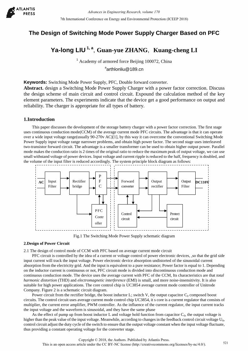
Company. Figure 2 is a schematic circuit diagram.
Power circuit from the rectifier bridge, the boost inductor L; switch V, the output capacitor C0 composed boost
circuits. The control circuit uses average current mode control chip UC3854, it’s core is a current regulator that consists of
multiplier, the current error amplifier, PWM controller. As the influence of the current regulator, the input current tracks
the input voltage and the waveform is sinusoidal, and they have the same phase
As the effect of pump up from boost inductor L and voltage hold function from capacitor C0, the output voltage is
higher than the peak value of the input voltage. Meanwhile, according to changes in the feedback control circuit voltage U0,
control circuit adjust the duty cycle of the switch to ensure that the output voltage constant when the input voltage fluctuate,
thus providing a constant operating voltage for the converter stage.
AC DC110V
PFC
Contr
oller
Control
circuit
Protect
circuit
Input
Filter
Rectifier
bridge
P
F
C
Forward
converter
Output
rectifier
Output
Filter
7th International Conference on Energy and Environmental Protection (ICEEP 2018)
Copyright © 2018, the Authors. Published by Atlantis Press. This is an open access article under the CC BY-NC license (http://creativecommons.org/licenses/by-nc/4.0/).
Advances in Engineering Research, volume 170
521
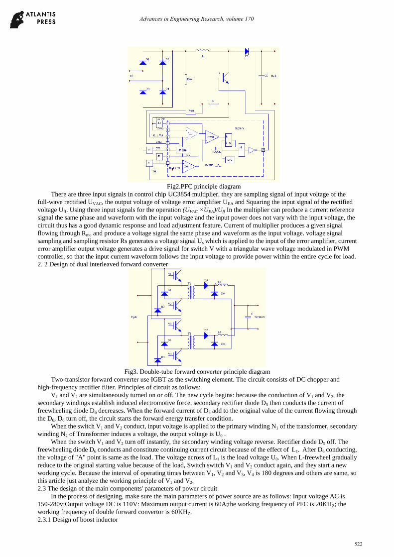
Fig2.PFC principle diagram
There are three input signals in control chip UC3854 multiplier, they are sampling signal of input voltage of the
full-wave rectified UVAC, the output voltage of voltage error amplifier UEA and Squaring the input signal of the rectified
voltage Uff. Using three input signals for the operation (UVAC ×UEA)/Uff In the multiplier can produce a current reference
signal the same phase and waveform with the input voltage and the input power does not vary with the input voltage, the
circuit thus has a good dynamic response and load adjustment feature. Current of multiplier produces a given signal
flowing through Rmo and produce a voltage signal the same phase and waveform as the input voltage. voltage signal
sampling and sampling resistor Rs generates a voltage signal Us which is applied to the input of the error amplifier, current
error amplifier output voltage generates a drive signal for switch V with a triangular wave voltage modulated in PWM
controller, so that the input current waveform follows the input voltage to provide power within the entire cycle for load.
2. 2 Design of dual interleaved forward converter
Fig3. Double-tube forward converter principle diagram
Two-transistor forward converter use IGBT as the switching element. The circuit consists of DC chopper and
high-frequency rectifier filter. Principles of circuit as follows:
V1 and V2 are simultaneously turned on or off. The new cycle begins: because the conduction of V1 and V2, the
secondary windings establish induced electromotive force, secondary rectifier diode D5 then conducts the current of
freewheeling diode D6 decreases. When the forward current of D5 add to the original value of the current flowing through
the D6, D6 turn off, the circuit starts the forward energy transfer condition.
When the switch V1 and V2 conduct, input voltage is applied to the primary winding N1 of the transformer, secondary
winding N2 of Transformer induces a voltage, the output voltage is U0 .
When the switch V1 and V2 turn off instantly, the secondary winding voltage reverse. Rectifier diode D5 off. The
freewheeling diode D6 conducts and constitute continuing current circuit because of the effect of L1. After D6 conducting,
the voltage of "A" point is same as the load. The voltage across of L1 is the load voltage U0. When L-freewheel gradually
reduce to the original starting value because of the load, Switch switch V1 and V2 conduct again, and they start a new
working cycle. Because the interval of operating times between V1, V2 and V3, V4 is 180 degrees and others are same, so
this article just analyze the working principle of V1 and V2.
2.3 The design of the main components' parameters of power circuit
In the process of designing, make sure the main parameters of power source are as follows: Input voltage AC is
150-280v;Output voltage DC is 110V: Maximum output current is 60A;the working frequency of PFC is 20KHZ; the
working frequency of double forward convertor is 60KHZ.
2.3.1 Design of boost inductor
Advances in Engineering Research, volume 170
522
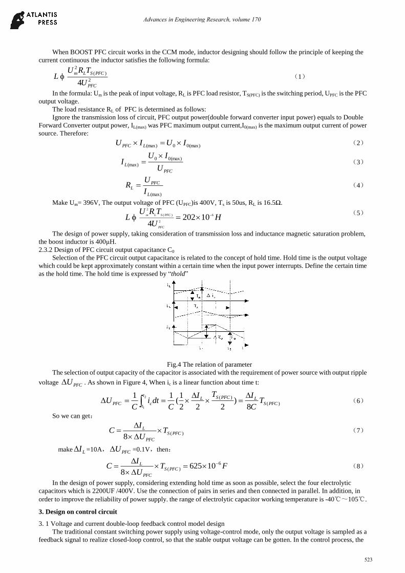
When BOOST PFC circuit works in the CCM mode, inductor designing should follow the principle of keeping the
current continuous the inductor satisfies the following formula:
2
)(
2
4 PFC
PFCSLm
U
TRUL (1)
In the formula: Um is the peak of input voltage, RL is PFC load resistor, TS(PFC) is the switching period, UPFC is the PFC
output voltage.
The load resistance RL of PFC is determined as follows:
Ignore the transmission loss of circuit, PFC output power(double forward converter input power) equals to Double
Forward Converter output power, IL(max) was PFC maximum output current,I0(max) is the maximum output current of power
source. Therefore:
(max)00(max) IUIU LPFC (2)
PFC
LU
IUI
(max)00
(max)
(3)
(max)L
PFCL
I
UR (4)
Make Um= 396V, The output voltage of PFC (UPFC)is 400V, Ts is 50us, RL is 16.5Ω.
HU
TRUL
PFC
PFCSLm 6
2
)(
2
102024
(5)
The design of power supply, taking consideration of transmission loss and inductance magnetic saturation problem,
the boost inductor is 400μH.
2.3.2 Design of PFC circuit output capacitance C0
Selection of the PFC circuit output capacitance is related to the concept of hold time. Hold time is the output voltage
which could be kept approximately constant within a certain time when the input power interrupts. Define the certain time
as the hold time. The hold time is expressed by “thold”
Fig.4 The relation of parameter
The selection of output capacity of the capacitor is associated with the requirement of power source with output ripple
voltage PFCU . As shown in Figure 4, When ic is a linear function about time t:
)(
)(
8)
222
1(
11 2
1PFCS
LPFCSLt
tcPFC T
C
ITI
Cdti
CU
(6)
So we can get:
)(8
PFCS
PFC
L TU
IC
(7)
make LI =10A, PFCU =0.1V,then:
FTU
IC PFCS
PFC
L 6
)( 106258
(8)
In the design of power supply, considering extending hold time as soon as possible, select the four electrolytic
capacitors which is 2200UF /400V. Use the connection of pairs in series and then connected in parallel. In addition, in
order to improve the reliability of power supply. the range of electrolytic capacitor working temperature is -40~105.
3. Design on control circuit
3. 1 Voltage and current double-loop feedback control model design
The traditional constant switching power supply using voltage-control mode, only the output voltage is sampled as a
feedback signal to realize closed-loop control, so that the stable output voltage can be gotten. In the control process, the
Advances in Engineering Research, volume 170
523
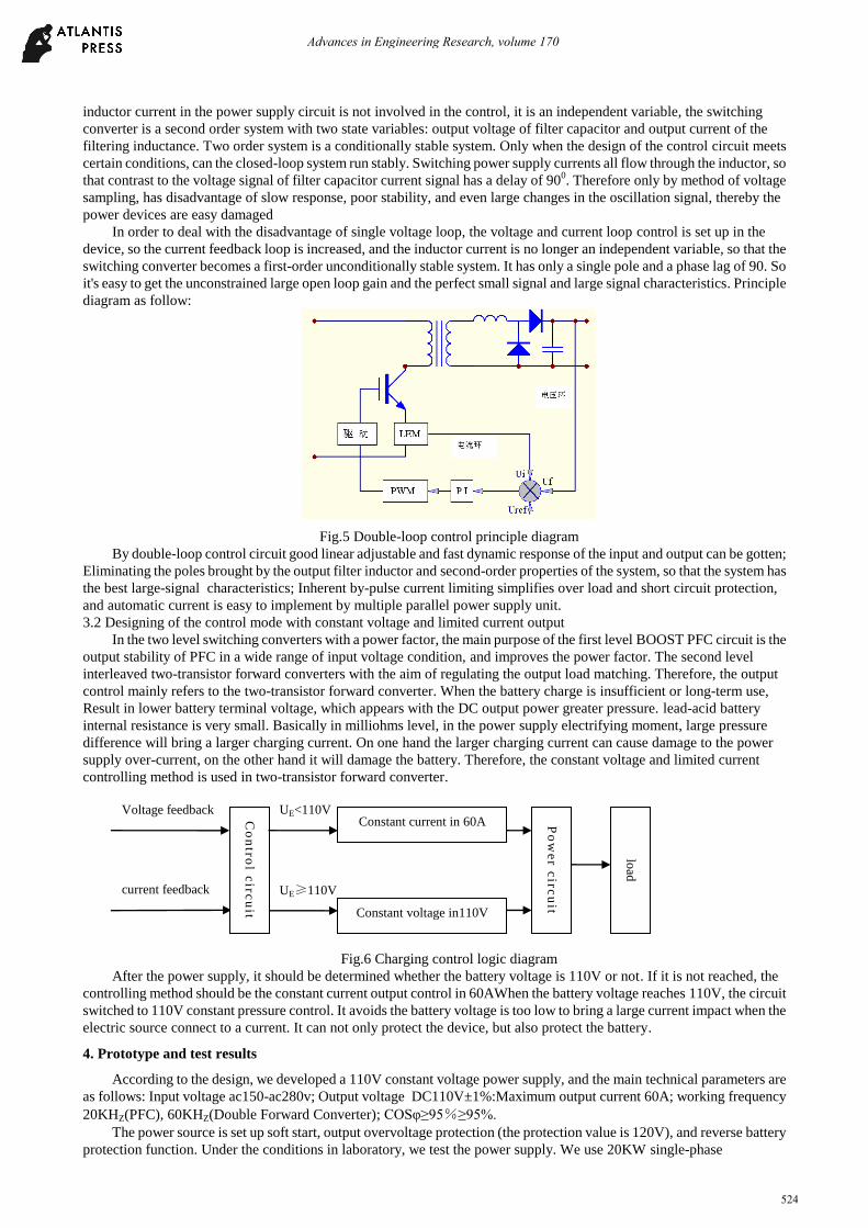
inductor current in the power supply circuit is not involved in the control, it is an independent variable, the switching
converter is a second order system with two state variables: output voltage of filter capacitor and output current of the
filtering inductance. Two order system is a conditionally stable system. Only when the design of the control circuit meets
certain conditions, can the closed-loop system run stably. Switching power supply currents all flow through the inductor, so
that contrast to the voltage signal of filter capacitor current signal has a delay of 900. Therefore only by method of voltage
sampling, has disadvantage of slow response, poor stability, and even large changes in the oscillation signal, thereby the
power devices are easy damaged
In order to deal with the disadvantage of single voltage loop, the voltage and current loop control is set up in the
device, so the current feedback loop is increased, and the inductor current is no longer an independent variable, so that the
switching converter becomes a first-order unconditionally stable system. It has only a single pole and a phase lag of 90. So
it's easy to get the unconstrained large open loop gain and the perfect small signal and large signal characteristics. Principle
diagram as follow:
Fig.5 Double-loop control principle diagram
By double-loop control circuit good linear adjustable and fast dynamic response of the input and output can be gotten;
Eliminating the poles brought by the output filter inductor and second-order properties of the system, so that the system has
the best large-signal characteristics; Inherent by-pulse current limiting simplifies over load and short circuit protection,
and automatic current is easy to implement by multiple parallel power supply unit.
3.2 Designing of the control mode with constant voltage and limited current output
In the two level switching converters with a power factor, the main purpose of the first level BOOST PFC circuit is the
output stability of PFC in a wide range of input voltage condition, and improves the power factor. The second level
interleaved two-transistor forward converters with the aim of regulating the output load matching. Therefore, the output
control mainly refers to the two-transistor forward converter. When the battery charge is insufficient or long-term use,
Result in lower battery terminal voltage, which appears with the DC output power greater pressure. lead-acid battery
internal resistance is very small. Basically in milliohms level, in the power supply electrifying moment, large pressure
difference will bring a larger charging current. On one hand the larger charging current can cause damage to the power
supply over-current, on the other hand it will damage the battery. Therefore, the constant voltage and limited current
controlling method is used in two-transistor forward converter.
Fig.6 Charging control logic diagram
After the power supply, it should be determined whether the battery voltage is 110V or not. If it is not reached, the
controlling method should be the constant current output control in 60AWhen the battery voltage reaches 110V, the circuit
switched to 110V constant pressure control. It avoids the battery voltage is too low to bring a large current impact when the
electric source connect to a current. It can not only protect the device, but also protect the battery.
4. Prototype and test results
According to the design, we developed a 110V constant voltage power supply, and the main technical parameters are
as follows: Input voltage ac150-ac280v; Output voltage DC110V±1%:Maximum output current 60A; working frequency
20KHZ(PFC), 60KHZ(Double Forward Converter); COSφ≥95%≥95%.
The power source is set up soft start, output overvoltage protection (the protection value is 120V), and reverse battery
protection function. Under the conditions in laboratory, we test the power supply. We use 20KW single-phase
Constant current in 60A
Constant voltage in110V
Po
we
r circ
uit
load
Co
ntro
l circ
uit
UE≥110V
UE<110V
current feedback
Voltage feedback
Advances in Engineering Research, volume 170
524
autotransformer as the input power supply, the input voltage by manual adjustment is between AC 150 to AC 280V. and we
use four 24V lead-acid batteries in series with the battery pack and 3Ω/10KW slider resistor in parallel. We adjust the
output power by adjusting the slider resistor values, then, the experimental results show, under the various conditions, the
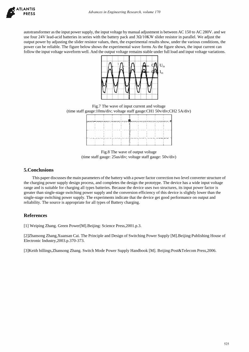
power can be reliable. The figure below shows the experimental wave forms As the figure shows, the input current can
follow the input voltage waveform well. And the output voltage remains stable under full load and input voltage variations.
Fig.7 The wave of input current and voltage
(time staff gauge:10ms/div; voltage staff gauge:CH1 50v/div;CH2 5A/div)
Fig.8 The wave of output voltage
(time staff gauge: 25us/div; voltage staff gauge: 50v/div)
5.Conclusions
This paper discusses the main parameters of the battery with a power factor correction two level converter structure of
the charging power supply design process, and completes the design the prototype. The device has a wide input voltage
range and is suitable for charging all types batteries. Because the device uses two structures, its input power factor is
greater than single-stage switching power supply and the conversion efficiency of this device is slightly lower than the
single-stage switching power supply. The experiments indicate that the device get good performance on output and
reliability. The source is appropriate for all types of Battery charging.
References
[1] Weiping Zhang. Green Power[M].Beijing: Science Press,2001.p.3.
[2]Zhansong Zhang,Xuansan Cai. The Principle and Design of Switching Power Supply [M].Beijing:Publishing House of
Electronic Industry,2003.p.370-373.
[3]Keith billings,Zhansong Zhang. Switch Mode Power Supply Handbook [M]. Beijing:Post&Telecom Press,2006.
CH1 Uin
CH2 Iin
Advances in Engineering Research, volume 170
525