Embed Size (px)
Citation preview

-.I
m.-
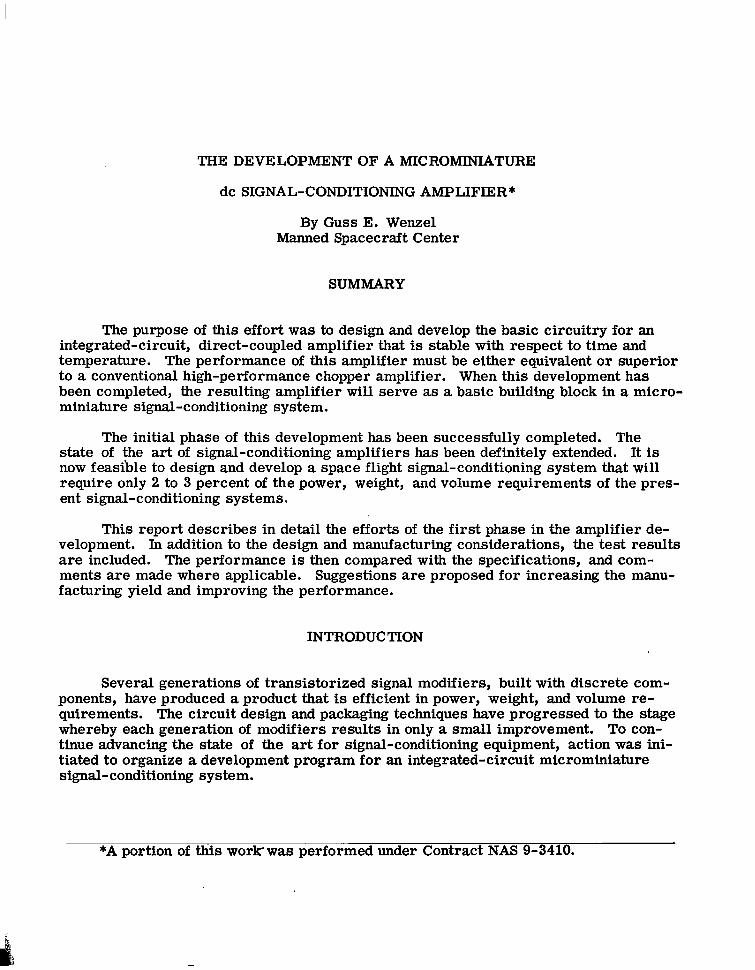
THE DEVELOPMENT OF A MICROMINIATURE dc SIGNAL-CONDITIONING AMPLIFIER
by Guss E. Wenzel
Manned Spacecraft Center Houston, Texas
. '. . ,
. ,
N A T I O N A L AERONAUTICS A N D SPACE A D M I N I S T R A T I O N W A S H I N G T O N , D. C. JULY 1967 iiii
https://ntrs.nasa.gov/search.jsp?R=19670022657 2020-03-24T01:39:44+00:00Z

I 111ll TECH LIBRARY KAFB, NM
I Ill11lllllIlls llllllllllIll11111 0330939
THE DEVELOPMENT OF A MICROMINIATURE
dc SIGNAL-CONDITIONING AMPLIFIER
By G u s s E. Wenzel
Manned Spacecraft C e n t e r Houston, Texas
N A T I O N A L AERONAUTICS AND SPACE ADMINISTRATION
For sale by the Clearinghouse for Federal Scientific and Technical Information Springfield, Virginia 22151 - CFSTI price $3.00

ABSTRACT
This report details design and development of the basic circuitry for an integrated-circuit direct-coupled amplifier that is stable with respect to time and temperature. The amplifier serves as a basic building block in a microminiature signal-conditioning system.
ii

CONTENTS
Section Page
SUMMARY . . . . . . . . . . . . . . . . . . . . . . . . . . . . . . . . . . . . . 1
INTRODUCTION . . . . . . . . . . . . . . . . . . . . . . . . . . . . . . . . . . 1
SYMBOLS . . . . . . . . . . . . . . . . . . . . . . . . . . . . . . . . . . . . . 3
MANUFACTURING CONSIDERATIONS . . . . . . . . . . . . . . . . . . . . . . 4
COMPLIANCE TO SPECIFICATIONS . . . . . . . . . . . . . . . . . . . . . . . 5
Supply Voltage Conditions . . . . . . . . . . . . . . . . . . . . . . . . . . . 6
Temperature Range . . . . . . . . . . . . . . . . . . . . . . . . . . . . . . 6
Service Life . . . . . . . . . . . . . . . . . . . . . . . . . . . . . . . . . . 6
Warmup Time . . . . . . . . . . . . . . . . . . . . . . . . . . . . . . . . . 7
Input Signal . . . . . . . . . . . . . . . . . . . . . . . . . . . . . . . . . . . 7
Input Impedance . . . . . . . . . . . . . . . . . . . . . . . . . . . . . . . . 7
Output Bias and Offset . . . . . . . . . . . . . . . . . . . . . . . . . . . . . 7
Output Signal . . . . . . . . . . . . . . . . . . . . . . . . . . . . . . . . . . 8
Output Impedance . . . . . . . . . . . . . . . . . . . . . . . . . . . . . . . 9
Voltage Gain . . . . . . . . . . . . . . . . . . . . . . . . . . . . . . . . . . 9
Gain Stability and Frequency Response . . . . . . . . . . . . . . . . . . . . 9
Output Ripple . . . . . . . . . . . . . . . . . . . . . . . . . . . . . . . . . . 9
Linearity . . . . . . . . . . . . . . . . . . . . . . . . . . . . . . . . . . . . 10
Grounding Procedure . . . . . . . . . . . . . . . . . . . . . . . . . . . . . 10
CommonMode . . . . . . . . . . . . . . . . . . . . . . . . . . . . . . . . . 10
Volume . . . . . . . . . . . . . . . . . . . . . . . . . . . . . . . . . . . . . 10
CONCLUSIONS . . . . . . . . . . . . . . . . . . . . . . . . . . . . . . . . . . 10
iii
I

Section Page
APPENDIX A -AN INTEGRATED dC DIFFERENTIAL INSTRUMENTATION AMPLIFIER . . . . . . . . . . . . . 33
APPENDIX B -SPECIFICATIONS FOR A MICROMINIATURE dc AMPLIFIER . . . . . . . . . . . . . . . . . . . . . . . . . 53
REFERENCES . . . . . . . . . . . . . . . . . . . . . . . . . . . . . . . . . . . . 56
iv

TABLE
Table Page
I CHARACTERISTICS FOR FLAT-PACK INTEGRATED DIFFERENTIAL AMPLTFIER . . . . . . . . . . . . . . . . . . . . . 12
FIGURES
Figure Page
1
2
3
10
11
12
13
14
15
16
17
18
19
Die. multicircuit subassembly . . . . . . . . . . . . . . . . . . . . . 13
MCD philosophy . . . . . . . . . . . . . . . . . . . . . . . . . . . . . 14
Division of circuit into integrable sections . . . . . . . . . . . . . . . 15
Amplifier. direct.coupled. input chip . . . . . . . . . . . . . . . . . 16
DC amplifier input stage . . . . . . . . . . . . . . . . . . . . . . . . 17
Amplifier. direcbcoupled. output stage . . . . . . . . . . . . . . . . 18
Outputstage . . . . . . . . . . . . . . . . . . . . . . . . . . . . . . . 19
Amplifier. direcbcoupled. common-mode stage . . . . . . . . . . . . 20
Commonmode . . . . . . . . . . . . . . . . . . . . . . . . . . . . . . 21
Amplifier. direct.coupled. drift-offset stage . . . . . . . . . . . . . 22
DC amplifier drift offset . . . . . . . . . . . . . . . . . . . . . . . . 23
Amplifier. direct.coupled. voltage regulator (VR-01) . . . . . . . . . 24
Voltage regulator (VR-01) . . . . . . . . . . . . . . . . . . . . . . . . 25
Amplifier. direcbcoupled. voltage regulator (VR-02) . . . . . . . . . 26
Voltage regulator (VR-02) . . . . . . . . . . . . . . . . . . . . . . . . 27
Amplifier. direct.coupled. feedback resis tor subassembly . . . . . . 28
Feedback resistor subassembly . . . . . . . . . . . . . . . . . . . . . 29
Capacitor a r r ay . . . . . . . . . . . . . . . . . . . . . . . . . . . . . 30
Capacitor networks . . . . . . . . . . . . . . . . . . . . . . . . . . . 31
V

Figure Page
20 Photograph showing how a fuse link is opened
(a) Before . . . . . . . . . . . . . . . . . . . . . . . . . . . . . . . . 32 (b) After . . . . . . . . . . . . . . . . . . . . . . . . . . . . . . . . . 32
21 Package drawing . . . . . . . . . . . . . . . . . . . . . . . . . . . . . 33
22 Package layout drawing . . . . . . . . . . . . . . . . . . . . . . . . . 34
23 Warmup time . . . . . . . . . . . . . . . . . . . . . . . . . . . . . . 35
24 Zero drift versus yield characteristics . . . . . . . . . . . . . . . . . 35
25 Output capability . . . . . . . . . . . . . . . . . . . . . . . . . . . . . 36
26 Frequency response . . . . . . . . . . . . . . . . . . . . . . . . . . . 36
27 Common-mode rejection . . . . . . . . . . . . . . . . . . . . . . . . 37
28 Linearity . . . . . . . . . . . . . . . . . . . . . . . . . . . . . . . . . 37
A-1 Overall emitter feedback . . . . . . . . . . . . . . . . . . . . . . . . 49
A-2 Differential equivalent circuit . . . . . . . . . . . . . . . . . . . . . . 49
A-3 Overall base feedback . . . . . . . . . . . . . . . . . . . . . . . . . . 49
A-4 Complete amplifier . . . . . . . . . . . . . . . . . . . . . . . . . . . 50
A-5 Package layout . . . . . . . . . . . . . . . . . . . . . . . . . . . . . . 51
vi
THE DEVELOPMENT OF A MICROMINTATURE
dc SIGNAL-CONDITIONING AMPLIFIER*
By Guss E. Wenzel Manned Spacecraft Center
SUMMARY
The purpose of this effort was to design and develop the basic circuitry for an integrated-circuit, direct-coupled amplifier that is stable with respect to time and temperature. The performance of this amplifier must be either equivalent o r superior to a conventional high-performance chopper amplifier. When this development has been completed, the resulting amplifier will serve as a basic building block in a microminiature signal-conditioning system.
The initial phase of this development has been successfully completed. The state of the art of signal-conditioning amplifiers has been definitely extended. It is now feasible to design and develop a space flight signal-conditioning system that will require only 2 to 3 percent of the power, weight, and volume requirements of the present signal-conditioning systems.
This report describes in detail the efforts of the first phase in the amplifier development. In addition to the design and manufacturing considerations, the test results are included. The performance is then compared with the specifications, and comments a r e made where applicable. Suggestions a r e proposed for increasing the manufacturing yield and improving the performance.
INTRODUC"ION
Several generations of transistorized signal modifiers, built with discrete components, have produced a product that is efficient in power, weight, and volume requirements. The circuit design and packaging techniques have progressed to the stage whereby each generation of modifiers results in only a small improvement. To continue advancing the state of the art for signal-conditioning equipment, action was initiated to organize a development program for an integrated-circuit microminiature signal- conditioning system.
*A portion of this work' was performed under Contract NAS 9-3410.

The basic circuit required in the design of a signal-conditioning system is a direct-current (dc) amplifier that is stable with respect to time and temperature. Although direct-coupled amplifiers have been stabilized by numerous methods with var i ous degrees of success, the most successful method of dc amplification has been the chopper amplifier. The chopper amplifier is successful because the signal through the amplifier is an amplitude-modulated square wave and, therefore, can be amplified byresistance-capacitance-coupled stages of gain. This type of design does not amplify the drift in quiescent voltages as does a direct-coupled amplifier. The main disadvantage to the direct-coupled amplifier, built with discrete components, is the problem of maintaining carefully matched temperature -sensitive components at the same temper ature. Because of the physical size of these components, it is extremely difficult to maintain an acceptable match. This temperature mismatch, or gradient, will result in a shift in the quiescent points and will appear effectively as a signal. This signal will be amplified then by all of the following stages of gain and will appear at the amplifier output as an e r r o r in the signal.
An integrated-circuit amplifier overcomes the temperature-gradient problem of direct-coupled amplifiers that are built with discrete components because all of the components are essentially at the same temperature since the complete circuit is so small. This type of design will be complicated by the lack of potentiometers and similar devices. However, this restriction can be overcome by careful planning of the design.
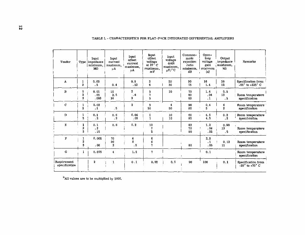
Several manufacturers have designed and produced a limited number of microminiature dc amplifiers. An analysis of the data of a recently conducted market su r vey, tabulated in table I, indicates that no company produces an amplifier similar to one which would meet the requirements for use in space flight. These data indicate, and further investigation has confirmed, that an acceptable amplifier can be designed with integrated circuits if a reasonable amount of effort is applied. A detailed description of an integrated dc differential instrumentation amplifier is shown in appendix A.
The dc signal-conditioning amplifier development program is set up to be accomplished in two phases. The first phase is to develop the basic circuitry. Specifications were formulated to reflect typical or worst-case actual flight requirements (appendix B). With this type of amplifier design perfected, it becomes a relatively simple matter to make modifications for the various gain and frequency response requirements for actual flight use. The second phase of the development is to improve the design of the first phase. In a discrete component design, this phase would be neither required nor desired because the circuit design engineer would have sufficient background cir cuit history to formulate his decisions. However, in advancing the state of the a r t by using integrated circuits, this background is not available, and the first design may not necessarily be the best design. This phase is considered to be very important because it will allow the circuit design engineer to reconsider the first-phase design. In addition to a reevaluation of the basic design, phase two will help the engineer broaden the specification requirements to insure proper operation in space flight environments and will help to reduce the product cost by allowing consideration of methods for reduction of circuit complexity and of increasing the manufacturing yield.
The packaging of the amplifier does not advance the state of the art. A conventional flat pack was used in the same manner that digital circuits are packaged.
2
Appendix A of this paper was prepared by David Roy Breuer, TRW Systems Group, Redondo Beach, California.
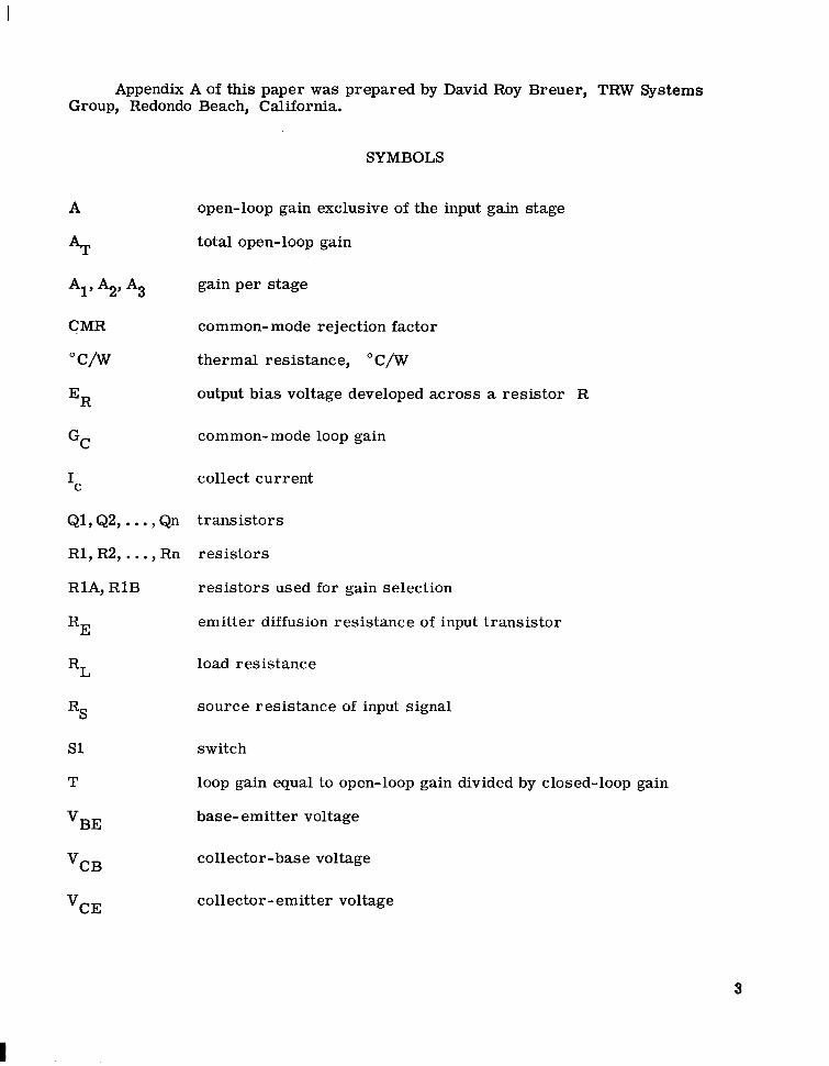
SYMBOLS
A open-loop gain exclusive of the input gain stage
AT total open-loop gain
AI, A29 A3 gain per stage
CMR common-mode rejection factor
O c/w thermal resistance, "C/W
ER output bias voltage developed across a resistor R
GC common- mode loop gain
collect currentI C
Q1, Q2, ...,Qn transistors
R1, R2,. ..,Rn resistors
RlA, R1B resistors used for gain selection
RE emitter diffusion resistance of input transistor
RL load resistance
RS source resistance of input signal
s1 switch
T loop gain equal to open-loop gain divided by closed-loop gain
V~~ base-emitter voltage
VCB collector-base voltage
VCE collector- emitter voltage
3

vcs collector -substrate voltage
VR voltage regulator
Vi input -signal voltage
V0
output-signal voltage
'in(CM) common-mode input impedance
13 current gain of the input transistors
*ICBO collector-base leakage current difference of the two input transistors
MANUFACTURING CONSIDERATIONS
The most ideal design would be to manufacture the entire amplifier on a single silicon die. However, because of yield purposes, the amplifier was designed by using eight separate dice. Careful division of the circuitry permitted a common transistor substrate, named the multicircuit die (MCD), to be used in providing the different dice at a minimum cost. In figure 1, the mask layout of the MCD with its 12 transistors, 4circui t crossovers, and 1test transistor is shown. The MCD is put to practical use with the aid of the four special masks shown in figure 2. These masks are used to vacuum-deposit the resistors and interconnections necessary to produce a specific c i r cuit.
The various dice in relation to the complete amplifier schematic diagram are shown in figure 3. A breakdown of these dice is as follows:
Die I Function I MCD Transistors Resistors Capacitors RA-01 Resistor array No 0 9 0 DM-02 Input amplifier Yes 9 8 0
CA-01 Capacitor array No 0 0 4 DM-O1A Output amplifier Yes 12 15 0 VR-02 Voltage regulator Yes 11 9 0 VR-01 Voltage regulator Yes 10 9 0 Do-01 Drift offset control Yes 6 15 0
CM-01 Common-mode amplifier Yes 6 1 2 0
8 Complete amplifier --- 54 77 4
4
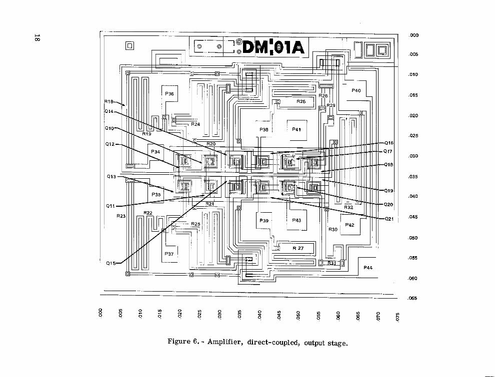
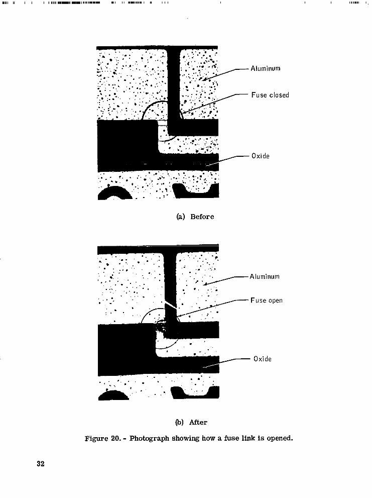
The photographic mask layout of these dice and the schematics a re presented in figures 4 to 19. A n analysis of these drawings shows that some resis tors can be adjusted for optimum amplifier performance. The adjustment technique is as follows: the main portion of the resistor is made a few percent smaller than the design value; in series with this resistor a r e several smaller resistors that are shorted by aluminum fuse links; the exact resistance required for optimum amplifier performance is determined by a test condition; then this value of resistance is obtained by opening the corresponding fuse links with high-current pulses. Figure 20 is a photograph of a fuse link before and after opening. In the same manner, the capacitors are adjustable by a parallel layout.
The previously mentioned eight dice are mounted in a flat package with a high-temperature epoxy (fig. 21). The dice are interconnected and connected to the flat-package leads with the 1.5-mil gold wire as illustrated in figure 22.
The amplifier is energized with power supply voltages and stimulated with an input signal. Various tests a r e conducted to determine the values of the adjustable resistors and capacitors. After these vdues a r e selected, the amplifier is sealed and acceptance- tested.
A summary of the manufacturing sequence is as follows:
1. Manufacture, select, and stockpile MCD wafers; each wafer contains approximately 125 dice.
2. Generate the four photographic masks required to produce a specific circuit and process the wafers.
3. Test and catalog each die. (Each die has a serial number.)
4. Separate and sor t the dice.
5. Mount the dice in the flat pack and interconnect with 1.5-mil gold wire.
6. Test and select the adjustable resistors and capacitors.
7. Seal the package and perform acceptance tests.
COMPLIANCE TO SPECIFICATIONS
The specifications for the development of the direct- coupled amplifier are derived from either typical or worst-case actual flight requirements, depending on the component being considered and the conditions to which it will be subjected. With this philosophy as a basis for design, the resultant equipment can be used or easily modified with the assured success of producing amplifiers suitable for future spacecraft applications.
The following paragraphs present a detailed listing of these specifications with suitable comments and actual laboratory test data.
5
Supply Voltage Conditions
The nominal voltage and current is to be selected by the circuit designer. This voltage may vary by k5 percent over a frequency range of from dc to 100 kHz.
The intent of this specification is to assure that the circuit design engineer, who would be the best qualified person, would be able to select the supply voltages most desirable for the design. In actuality, the engineer must consider eventually the fact that he cannot have an ideal supply source. For the design effort, the maximum current drain on this supply was omitted purposely to provide the engineer with an opportunity to produce the best design instead of a less desirable performance design based on insufficient current. Test data show that the power requirements a r e about 150 mW from a 3-terminal, +9- and -9-V supply. The data also show that a 5-percent change in supply voltage yields approximately a 25- to 37-mV change in the amplifier zero setting. In actual use, it is anticipated that this supply voltage will change by less than 0.5 percent and, therefore, will cause a change in amplifier zero setting of 2 to 3 mV.
Temperature Range
The module must start and operate at any constant o r variable (20" F/min maximum) temperature from -30" to +200° F. The module must not be damaged when subjected to a nonoperating storage of at least 6 hours at any temperature from -65" to +250" F.
Since the design consists of several integrated-circuit chips, storage temperatures are not a problem. In fact, the amplifier could be stored at any temperature from -65" to +300° F without damage. Because of the small size of the chips, which result in small temperature differences of critically matched components, a variable temperature does not appear to be a problem. Figures for the maximum spacecraft temperature gradient are not available now, but 20" F/min or less appears to be realistic. The heat-dissipation characteristic of the amplifier is satisfactory, and overheating does not occur within the operating temperature range. Performance of the amplifier within this range is discussed in the sections entitled "Output Bias and Offset" and "Gain Stability and Frequency Response. I '
Service Life
The module must be capable of operating for a minimum of 2000 hours, continuously o r otherwise, during a service life of 1year.
Since the amplifier design does not contain any moving parts o r parts that will wear out, the life expectancy will be very long. It would be possibly as long as 100 000 hours. One amplifier has operated 5000 hours in a life test, and no change in characteristics has been evident.
6

Warmup Time
The module must be capable of operation with a warmup time not to exceed 50 psec.
The amplifier design is such that the warmup time is well within specifications. Several units were tested by turning the power off and on with a mercury relay and observing the amplifier output signal referenced to the supply voltage on an oscilloscope. Figure 23 is a plot of the warmup characteristics of several amplifiers.
Input Signal
The module must be capable of receiving variable differential input signals from 0 to lt5 V without damage.
In normal use, the maximum input signal will be about 7.1 mV for full-scale output. This specification w a s included to protect the amplifier from destruction by larger signals. The breakdown voltage of the input transistors is approximately 7 V. Therefore, a 5-V signal can be tolerated without destruction. If protection is desired for greater voltages, it can be obtained by adding protection diodes to the input circuit. However, diodes will introduce an additional source of e r ror and reduce the performance characteristics. It is significant that a single-ended signal can be applied to the amplifier, but this will result in a shift in the amplifier zero setting. A correction can be made for amplifiers used in this mode.
Input Impedance
The input impedance must be 50 000 52 o r greater for any gain setting and for any frequency from dc to 5000 cps. A base current not exceeding 0.2 PA must be supplied internally to accommodate a floating source.
The input impedance to the amplifier proper is from 15 to 40 M a , depending, among other things, upon the gain setting and the temperature. However, a biasing circuit is required to accommodate a floating-signal source. With respect to the amplifier input terminals, this biasing circuit appears as two series-connected 50 000-52 resis tors that are in parallel with the input impedance to the amplifier proper. Since this impedance is large compared to the biasing impedance, the terminal amplifier input impedance becomes essentially the value of the biasing resistors, which is 100 000 52.
Output Bias and Offset
With a zero-input signal from a floating-source impedance of from 0 to 375 52, the module output must be capable of being set to 0 or 2.5 V. Selection must be by moving jumper wires between external leads. This output voltage must be within +50 mV of the ideal value over the environment range specified.
7

The difference in base currents of the two input transistors is the current that flows through the signal source. The base current of these transistors is 0.2 pA, but this may change by A 0 percent because of the manufacturing tolerances of the transistors. Therefore, worst-case conditions would result in a 0.04 pA current through the source. The voltage developed by this current through the source resistance appears as a differential signal to the amplifier input. For a fixed-source impedance, this error can be canceled out within the amplifier. However, a variable-source impedance will result in a shift in the amplifier zero setting. For example, assume a condition in which a source impedance would change from 0 to 1000 52. The worst-case shift in zero setting at a gain of 1000 would be 40 mV. This shift would be the majority of the e r ro r allowed by the specifications. Because of this, it was concluded that a specification requirement of a 0- to 3 7 5 4 source (that could result in a 15-mV shift in the output) was a realistic requirement that could be accomplished. It has been determined in laboratory tests that the zero shift between 0 and 350 52 is from 4 to 12 mV with an average of about 8 mV. The adjustments of the zero setting and the 2.5-V bias setting are satisfactory because these can be set easily to within 5 mV of the desired values. The temperature characteristic of the 2.5-V bias supply also appears to be satisfactory. The temperature characteristics of the zero setting, however, are not as satisfactory as desired. The test data, recorded in figure 24, indicate that from -30" to +200"F only 50 percent of the amplifiers are capable of being temperature-compensated to remain within the 1percent allowed by the specifications. The remaining 50 percent may drift as much as 3 percent. All amplifiers could be compensated, however, to within 1 percent if the temperature range were reduced to the range of 0" to 160" F. An investigation of this problem has revealed that i t is not serious for the reasons stated in the following paragraph.
The uncompensated amplifier has a nearly linear temperature coefficient. The bridge-arranged compensation circuit also appears to have a linear temperature coefficient. However, loading the bridge by the amplifier results in a nonlinear overall characteristic. The amount of this nonlinearity is a direct function of the current requirements of the uncompensated amplifier. This problem has been recognized and a solution formulated. Briefly, the solution is as follows.
Future fabrication will use transistors that are more closely matched and that have higher current gains. In addition, a new compensation circuit consisting of trans is tors and diodes will be developed to provide the required amount of linear temperature compensation.
Output Signal
The module must be capable of delivering output signals of from 0 to t 5 V with the output bias set at either 0 o r +2.5 V to a load of from 50 000 52 to open circuit.
The amplifier design is such that this specification is met easily. In fact, output signals of greater than *5 V can be amplified, as figure 25 indicates. In addition, the amplifier's output impedance is sufficiently low and has current capabilities to drive a load of 5000 52 with loading effects of less than 1 percent.
8
Output Impedance
The output impedance of the module must not exceed 100 52 from dc to 5000 cps.
The amplifier output impedance has been measured to be consistently less than 10 52, with the average centered around 5 52.
Voltage Gain
The voltage gain must be adjustable in steps within 1 percent of the ideal values of 700, 850, and 1000 V. This adjustment must consist of jumper wires connected between identified leads. No components may be added to chdnge from one gain setting to another.
There is no problem in setting the gain to the l-percent specification. In fact, most of the ranges can be set to better than 0.1 percent of the ideal value.
Gain Stability and Frequency Response
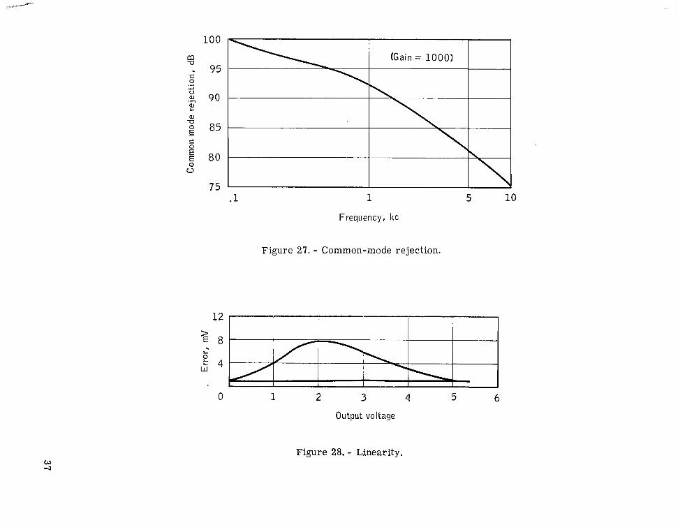
The gain of the module must be within t l percent of the dc value at 75" F from dc to 5000 cps. The frequency response must not change more than + lpercent over the specified environment range.
As shown in figure 26, the frequency response of the amplifier is much greater than is required. It is desirable to reduce this response in future fabrication because the net effect will be to reduce the ripple on the output signal. There is no problem in modifying this response because the only change will be to increase the s ize of a capacitor. There is sufficient space within the amplifier to accommodate a larger capacitor. The gain stability of the amplifier did not meet the specification requirements. Typical variations were found to be from 1 to 2 percent. The variation is due to higher transistor-emitter, parasitic resistance than anticipated in the initial fabrication. The results are that typical open-loop gains are between 20 000 and 30 000 rather than the design value of 100 000. This can be corrected easily in future processing runs and is not considered a serious problem.
Output Ripple
The maximum output ripple voltage must be 25 mV peak to peak from dc through 15 Mc with a 90-percent confidence level measured over a period of 1 sec.
The amplifier design is such that this parameter is marginal. Typical amplifiers were measured to have an output ripple of 20 to 30 mV peak to peak. With the frequency response of the amplifier reduced as described above, this ripple will be reduced also. Therefore, this marginal design is not considered to be a problem.
9

Linearity
The module must have a linear output within lt12.5 mV of a straight line between the end points (nominal 0 and +5 V) with the output bias set at either 0 or +2. 5 V.
The amplifiers exhibited a very good linearity curve, one that was well within the specification (fig. 27). With the higher open-loop gain as described for future fabrication, the linearity will be further improved.
Grounding Procedure
The signal input must be of the differential type and must accommodate a floating source. No external-input ground reference will be needed.
The amplifier design meets this specification. In addition, there are provisions through which a center-tapped source could be connected to the amplifier if the need ever occurs.
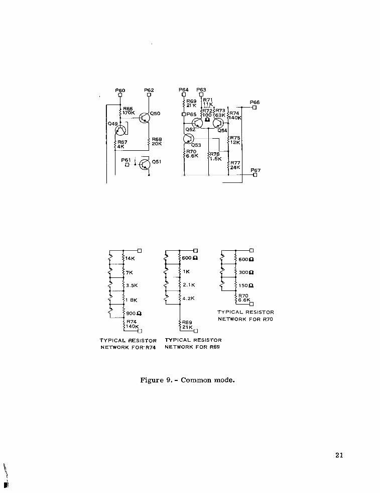
Common Mode
The module must have a common-mode rejection ratio of 80 dB o r more for a 0- to 375-52 floating-source resistance for frequencies from dc to 5000 cps and for voltages of * l . O V.
The design of the amplifier is satisfactory to meet the requirements of this specification, as indicated in figure 28. This characteristic will improve with a single-gain version because the common-mode rejection can be optimized for this gain rather than having a compromise for several gain settings.
Volume
The module must be 0.01 cu in. o r less.
This specification was met by mounting the eight microminiature chips in a container 0.375 by 0.375 by 0.07 in. , or 0.01 cu in. Actually, single-gain amplifiers mounted in containers 0.375 by 0.25 by 0.07 in. , or 0.007 cu in., can be anticipated.
CONCLUSIONS
The development of a microminiature dc signal-conditioning amplifier has been completed with outstanding results, and the state of the art has been extended significantly. This development has proved that not only are signal-conditioning amplifiers of this nature feasible, but that with very little additional effort these amplifiers will be practical for use in space flight.
10
With no additional design effort, a limited number of flight-worthy amplifiers can be selected from a production lot. However, the test results indicate a need for improvement in the a reas of open-loop gain, temperature-compensation circuits, and frequency response. Although improvements in these areas are considered to be minor, they would be advantageous because they would allow significantly increased manufacturing yield.
An analysis of the problem areas has determined the exact portions of the circuits in which corrective actions are required. A change in process techniques will lower the emitter parasitic resistance and result in an increase in open-loop gain. This increase in gain wil l improve the time and temperature stability characteristics to a high degree. A teniperature- compensation circuit consisting of transistors, rather than resistance only, will improve the compensation characteristics. An increase in the value of the frequency-determining capacitor will reduce the amount of the output noise while maintaining the frequency response required by the specification.
Effort is being expended toward improving the dc amplifier in the form of ongoing work to incorporate the preceding suggestions. In addition, this effort will take into consideration the possibilities of simplifying the circuitry and extending the specification to include items such as output short-circuit protection and the capability of driving a load consisting of capacitance in addition to the required resistance.
Manned Spacecraft Center National Aeronautics and Space Administration
Houston, Texas, May 24, 1967 904-02-13-09-72
11
lnplt
TABLE I. - CHARACTERISTICS FOR FLAT-PACK INTEGRATED DIFFERENTIAL AMPLIFIERS
Input Common- Open-Input Input offset offset mode loop output
Vendor Type impedance current current voltage v:zg rejection voltage impedance Remarks Iat 25" C ratio gain maximum, maximum, m;udmumt minimum, , minimum, kS2 idB
/Lv'oc IE1
! 0.03 0.8 3
mV
20 90 16 10
i ~
Specification from
I I II A 2 .5 0.4 .12 6 30 75 1.4 12 -55" to +125" C I
2 5 10 70 1.4 0.5 I . 6 7 60 .04 13 Room temperature3 5 60 . 1 . 5 specification
0.02 2 5 4 90 0.4 6 Room temperature '
.1 .5 I 50 I 50 80 5 1 2 specification ~~ ~~
I -1 Room temperature I
c I
D 1 1
0.1 11
0.6 1 1
0.04 10 1 - 65 -1 4.5 -1 I ~ 0.2 specification2 . 2 .3 .02 85 4.5 . 2
.3 70 .04 13 E
2 1 I 0.1 I
I , 0.8
I ' 0.2 ~ 1;
I II
83 1.2 ! 0.90 I
Room temperature
F 4 80 .05
0.12 11
' Room temperature1 specification
G I
I 0.1 , Room temperaturespecification
Requirementspecification I , i
0 . 5 ' I
90
aAll values a re to be multiplied by 1000.
L 3 i .is 2

O O s 0 9 9 N 0 8 0 LD 00 8In g g 0 0 10 rO rLD N LD m LD e e Lo O L sDb9 9 9 9 9 9 I I I I 1 I I I I I I I I I I .om- ,
,050- ~
.OlO.
.015
.020- 1
.025
.030
.035
.040
. a 5
.OS0
.055
.060 -
.065 - I I

of 4 special masks
+ MCD
(semiconductor substrate)
\\
Ful l y integr'atebdkkcircuit
Figure 2. - MCD philosophy.
14

I I I
I I I I I
Figure 3. - Division of circuit into integrable sections.

.Ooo
lol .005
0 .010
.015
.020
.025
-45 .030
42- -.Q9 .035
.040
.045wRll
.050
.055
.060
.065
Figure 4. - Amplifier, direct-coupled, input chip.

F 7 6 14 Q 3 FP24
P
P 12 50K P 1 1ploxQ13.9K
R 1 1 50K P 14
P 13 0-7 4 P 2 1
P26~
P19 P20
Figure 5. - DC amplifier input stage.
-Qlt ,417
-OlE
-QlS
-Q2C
-921 I
,000
,005
.010
,015
.020
,025
.030
,035
,040
.045
,050
.055
.C60
,065
Figure 6. - Amplifier, direct-coupled, output stage.
1
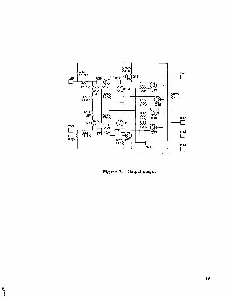
Figure 7.- Output stage.
19

m
,000
,005
,010
.015
.020
I1 I .025
Q52
049- .030
,035
.040\ ,045
,050
.055
P60 I ,060
.065
0 N O m 0 m 0 m 0 m 0 mo 0 2 2 0 m m d m m I\ ? ? ? ? ? ? ? ? 6 ? ? ? 8 : ? S
Figure 8. - Amplifier, direct-coupled, common-mode stage.
I I
949kT-4 I
1:3.5K
T Y P I C A L RESISTOR NETWORK FOR R70
T Y P I C A L RESISTOR T Y P I C A L RESISTOR NETWORK F O R ' R 7 4 NETWORK FOR R69
Figure 9. - Common mode.
21
I

I I I l l I l l
.ooo
.005
.010
.015
,020
.025
.030
.035
.040
.w5
.050
.055
.060
,065
Figure 10. - Amplifier, direct-coupled, drift-offset stage.

(EXTERNAL (EXTERNAL (-9) (-9) DIODE) DIODE)
0P59 U P 5 8 4 P 5 4 0P55
D R I F T CONTROL
800 1.6K
I u u
13.3K 13K 30 K
T Y P I C A L RESISTOR NETWORK FOR R54,R55, R56,R57, R61, R62,
R63 AND R64
P57 bP56 (OUTPUT) (OUTPUT)
Figure 11. - DC amplifier drift offset.

v)
v) N
1 .wo
.005
.010
.015
,020
-941 .025 -43 .030
.035
.040- Q3 .045
-Q31 .050
,055
,060
.065
0 m v) 0 0 m 0 v) 0 v)0 0 2 .- N W m d d v ) O 0
9 ? ? ? 9 9 ? ? ? 9 ? o e a s g
Figure 12. - Amplifier, direct-coupled, voltage regulator (VR-01).

P52
C - p i p j L 0
R46r $39K
4 3 5 I >
436
11OK
P53
P 5 1 -6
600
T Y P I C A L RESISTOR NETWORK FOR R43 AND R 4 4
4 3 4
R45 36 K
P50
R42 OR R45P30K OR 36K
1.2K
600
300 CL
150 P
7 5 n
T Y P l C A L RESISTOR NETWORK FOR R42 OR R45
Figure 13. - Voltage regulator (VR-01).
25
C

0
.OW
.005
a10
.015
.020
.025
.030
,035
.040
.045
Q50
,055
1 - 1 .060
. a 5
0 0 10 0 M 0 M 10 M M 0 in8 3 5 Qc 8 8 8 a : : 0. 8 8 2 G 6
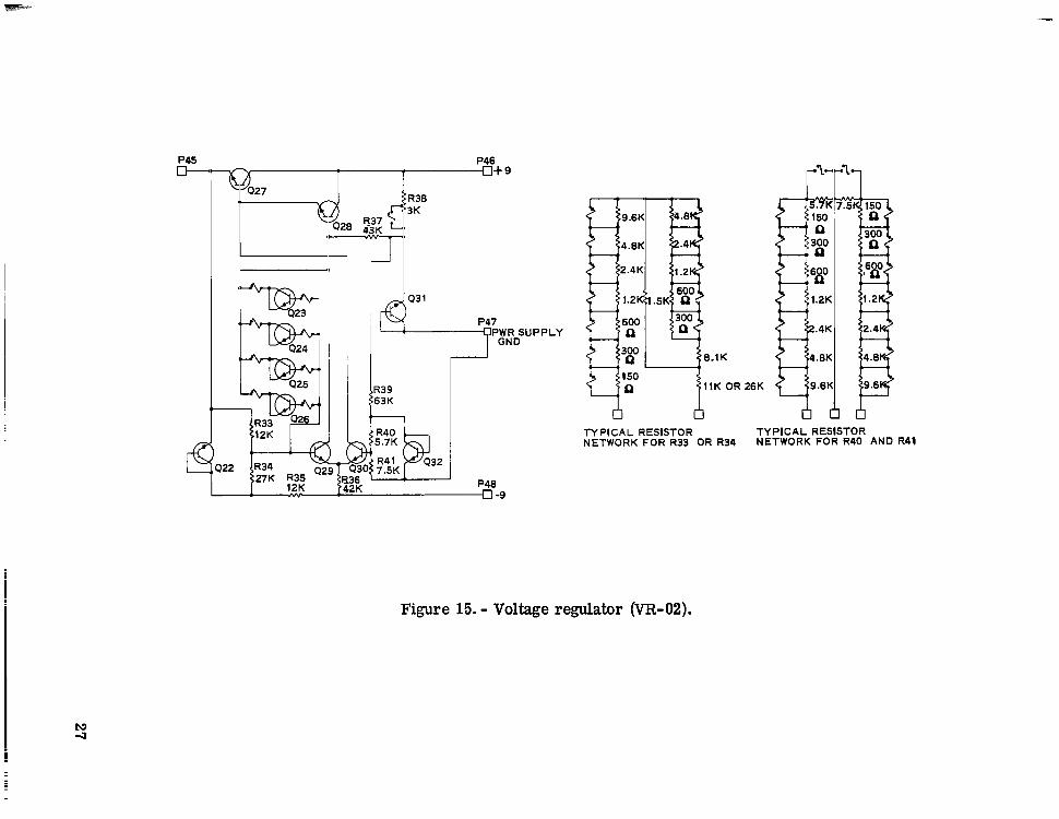
Figure 14. - Amplifier, direct-coupled, voltage regulator (VR-02).
P45 P46
-7 1.2%
4.8K
9.6F
PWR SUPPLY GND
150 11K OR 26K
I3 TYPICAL RESISTOR TYPICAL RESISTOR
I3 I3 NETWORK FOR R33 OR R34 NETWORK FOR R40 AND R4t
9
Figure 15. - Voltage regulator (VR-02).

,000
.005
,010
.015
.020
.025
,030
I R4 I
r-035
i .040
1.i .045
Q .050
.055
.060
.065
Figure 16. - Amplifier, direct-coupled, feedback resistor subassembly.

R7 R6 R5
4.8K
2.4K
1.2K 1.5K
600Q
300 $2
8.1K
1 T Y P I C A L RESISTOR
1 1.2K
600
3 0 0 a 1.5K
150q
8.1K
1
T Y P I C A L RESISTOR NETWORK FOR R3 AND R5 NETWORK FOR R1, R2, R6, AND R 7
Figure 17. - Feedback resistor subassembly.
29

u 0
Ptl
4 - 1 1
T 1rInr 1
r'in
.om
.005
.010
.015
.020
.025
.030
.035
.040
.045
,050
,055
Figure 18. - Capacitor array.

P27P P308'
P68 P28E P 8'b'P31 P32
P29
9 P33
Typical capacitor network for C4
Typical capacitor network for C1, C2, and C3
,
Figure 19. - Capacitor networks.
1111 I I1 I I I I11111 111111 1.111 1 1 1 1 1 1 1 1 1 .I I I .I,,,,,, I I, I I I I 11111.111 I
Aluminum
Fuse closed
' Oxide
(a) Before
9 . * . .- & . , . . . ... ... . - - a .e . - . *. . . . . ., :flAluminum . . ..' . . .,. *
* . a :. .
(b) After
Figure 20. - Photograph showing how a fuse link is opened.
32

Sym about
G
0.015f0.001 lead-width (typ) 0.063f 0.005
0.022f0.005
o .250'min typ 0.020f0.002
0.010 R max typ \ : 0.2301
L r
0.030 typ L O .005*0.001 - 0.005 max bleed over typ
0.050f0.005--- I 6 places
0.037 0.300 ref
0 . 3 7 5 f 0 . 0 1 0 4
W W Figure 21. - Package drawing.

G 1 A G 2A
El FlG3 A IN A
Fl OUTPUT"
0.375 SQUARE
G 16 G 26 G 36 IN 6 GRD +2.5 +9 (POWER SUPPLY)
Figure 22. - Package layout drawing.
34
I

I
1.o
.8 L e LW LI 8 a, .6 2W a
.4
.2
2 0 25 30 35 40
Microseconds
Figure 23. - Warmup time.
- 2
7t
// 100-percent yield
-3 0 7 5 Temperature, O F
160 200
Figure 24. - Zero drift versus yield characteristics.
35

I.6 .8 1 2 4 6 8 1 0 20 40 60 100 200 400 600 1000
Frequency, kc
Figure 26. - Frequency response.
36
50
40
30
20
>E 1 0
E o W Y
2 -10 Y 3 0
-20
-30
-4 0
-5 0
-5
100 80 60
40
20 Y S a,2 a,
," 10 g 83
O 6
4
2
1
I I7 1 1
I I I I-4-4-I II Iu-t-'nI I \ I
\1II .
- 4 - 3 - 2 - 1 0 1 2 3 4 5 6 7 Output vo I tage
Figure 25. - Output capability.
\ \ \
\
I I I
100
95
90
85
80
75 .1 1 5 10
Frequency, kc
Figure 27. - Common-mode rejection.
12 I-,-’- 1‘I
L
w eL 48!
0 1 2 3 4 5 6
Output voltage
Figure 28. - Linearity. w 4


APPENDIX A
AN INTEGRATED dc DIFFERENTIAL
INSTRUMENTATION AMPLIFIER
By David Roy Breuer
This appendix indicates some of the present capabilities of the integrated circuit in the field of high-accuracy linear amplification. Low drift, high common-mode rejection, and high stable gain can be achieved now in the integrated-circuit form by applying the design principles described.
The close matching of transistor characteristics and the thermal intimacy of all portions of the compatible integrated circuit make it uniquely attractive for applications requiring high dc accuracy over a wide environmental range. The design of high-performance amplifiers, however, is complicated by the lack of potentiometers, transformers, inductors, and large capacitors. Also, ac and dc parasitics must be considered carefully to insure stable operation.
The following discussion will include the circuit design philosophy, component characteristics, and fabrication techniques needed to produce an amplifier with these specifications:
1.
2.
3.
4.
5.
6.
7.
8.
Direct-coupled differential input and single-ended output
Operating temperature -35" to +95" C (assumed for all specifications)
Selectable gains of 700, 850, and 1000 within 1percent
Frequency response to insure 1percent accuracy up to 5 kHz
Equivalent input drifts down to 0 .2 pV/" C
Common-mode rejection ->lo0 dB for dc to 5 kc
Selectable output offsets of 0 o r +2. 5 V, accurate to within *50 mV
Input impedance >50 ks2, dc to 5 kHz, for floating sources; >10 Ma, dc to 5 kHz, for grounded sources
9. Output impedance <10 0, dc to 5 kHz
10. Output voltage swing of *5 V into 25 ks2 load impedance
11. Floating source impedance of 360 to 0 s2
12. Maximum quiescent input current into each input terminal of 200 nA
39

13. Power input of 100 mW
14. Power supply voltages may vary by kt5 percent
Feedback Techniques
Overall negative feedback from the output to the emitters of the input transistors, as shown in figure A-1, offers gain accuracy, low dc drift, minimum source-dependence, high input impedance, and low output impedance. Therefore, this emitter-type feedback is preferred for this application.
Switch S1, shown in figure A-I, is used to illustrate different modes of operation for the sake of discussion. In position 1, the amplifier is operating differential input and differential output. Assuming a perfectly balanced, symmetrical configuration, a differential-mode equivalent half circuit (ref. 1) can be drawn, as in figure A-2, to illustrate the differential-mode performance. The input stage is shown separate from the remaining portion of the amplifier. Analysis yields
Vo R1 + R 2 1 1 - = Vi R2
where RE = emitter diffusion resistance of input transistor, \<)A, and
A e open-loop gain exclusive of the input gain stage. ~fAT is very iarge, then
V o_ - R1 + R 2 V. - R21
which must always be greater than one.
The same gain equations apply to the case of switch S1 in positions 2 or 3 in which output B is effectively held at ground or ER, respectively. The single-ended
amplifier output A assumes the same potential as the reference for a zero differential input signal. This allows an offset to be applied to the amplifier output which is independent of gain setting.
The common-mode ,rejection for the single-ended and differential configurations are equal and dependent on the symmetry of the feedback impedances. For the particular design being considered, gain changes are mechanized by simultaneously selecting appropriate values for R1A and R1B. The gain is primarily determined by RlA, and R1B is correspondingly selected to give maximum common-mode rejection.
40

Since the common-mode rejection is particularly sensitive to the values of RlB, the +2.5-V reference supply required for this design must have a very low impedance to maintain maximum common-mode rejection for either output offset setting.
A block diagram of the overall base-type feedback connection which is used typically for operational amplifiers is shown in figure A-3. This configuration is unacceptable in this direct-coupled amplifier application because of the dc drift characteristics. To achieve closed-loop gains up to 1000, the feedback resis tors must be very large. The nonlinear temperature-dependent input base currents and collector-base leakage currents of the input transistors must flow through these large resistances, creating excessive nonlinear temperature-drift components. In contrast with overall emitter-type feedback, the base and leakage currents of the input transistors flow only throughthe source impedance, allowing the nonlinear drift components to become negligiblysmall.
Also, in the case of overall base feedback, the closed-loop gain is directly dependent upon the source impedance in ser ies with the feedback resistance R2. However, the closed-loop gain with emitter overall feedback is essentially independent of the source impedance. The closed-loop gain is affected by RS (only as it affects the open-loop gain).
For emitter feedback, the closed-loop differential input impedance is found from feedback analysis (ref. 2) to be equal to the open-loop input impedance multiplied by the loop gain T, where T is the open-loop gain divided by the closed-loop gain. The closed-loop output impedance is equal to the open-loop output impedance divided by T.
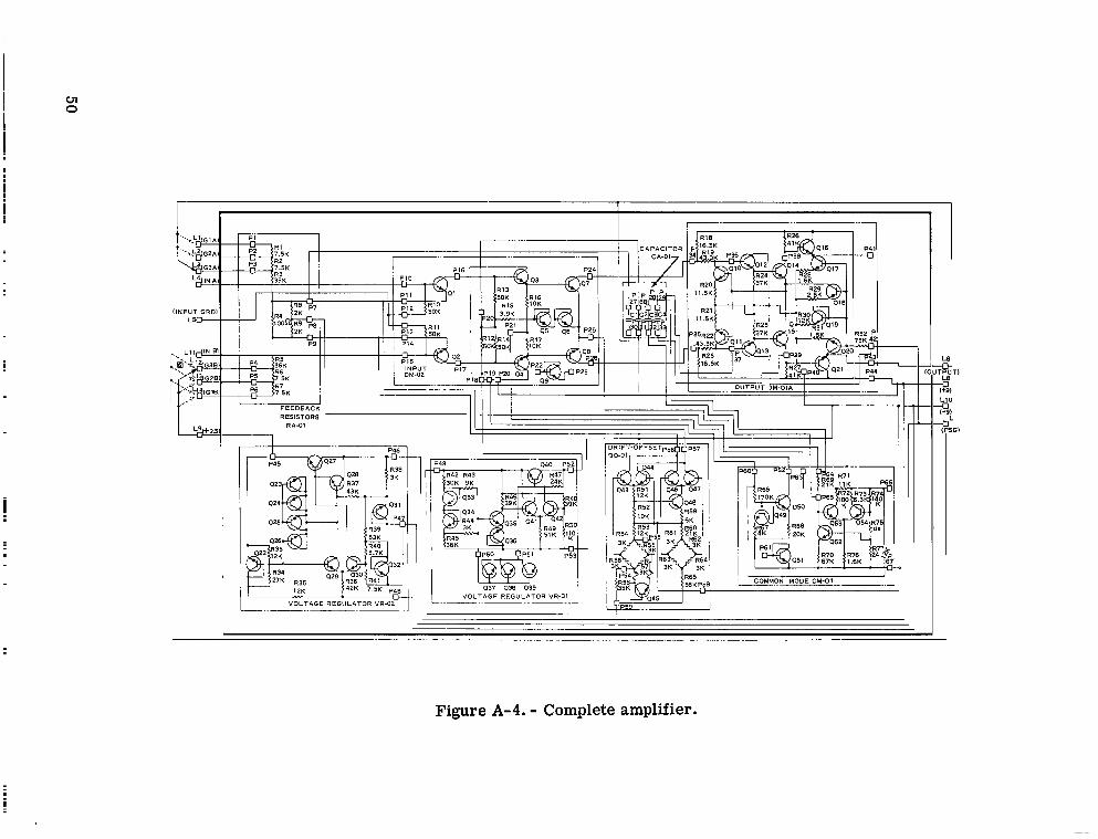
Drift Considerations
With reference to the schematic diagram of figure A-4, direct compensation is accomplished by supplying a temperature-dependent current from the drift-offset control circuit to flow through the feedback resistor R4. This adds a linear temperature-dependent voltage in ser ies with the input signal to cancel the accumulated inherent amplifier drift (ref. 3). The effectiveness of this drift compensation is directly related to the degree of linearity of the inherent and compensating drift components. Laboratory tes ts have shown equivalent input drifts less than 0.1 pV/"C.
The predominant drift components of a differential amplifier are generated in the input stage and are primarily caused by circuit parameter unbalances. The perfectlybalanced circuit would develop zero drift (and give infinite common-mode rejection).The main contributors to input-stage drift are differentials existing between the base-emitter voltages, current gains, and leakage currents of the input transistor pair. Each component is potentially nonlinear with temperature; however, with proper designtechniques, they can be either linearized o r minimized.
The differential collector-base leakage currents flowing through the source resistance develop the most nonlinear drift component, for it is proportional to the difference of two terms which increase exponentially with temperature. The silicon planar-diffused transistor of the present-day integrated circuit exhibits room temperature leakage currents of about 0 .1 nA. Assuming a doubling with every 11" C rise in
41

temperature, this current increases to 0 . 1 X 27 nA at +loo' C, which is less than 15 nA. For the 350-52 floating-source configuration, the e r r o r at +loo' C is
where AICBO is the collector-base leakage-current difference (in nanoamperes) of the two input transistors a t room temperature. This e r r o r is normally less than 2 to 3 pV and can be neglected. Note, however, that if overall base feedback were used, this drift term would have made the amplifier an impossibility.
Because of differential base currents, the most significant source-dependent drift term is caused by unequal transistor current gains which increase somewhat linearly with temperature. Assuming constant collector currents, the base currents decrease with increasing temperature. The voltage e r r o r is directly proportional to the source resistance and is minimized by the following:
1. Designing the input stage to operate a t very low collector current levels
2. Maximizing the current gains of the input transistors
3. Maximizing the current gain match of the input transistors
Given the 200-nA input current specification, with minimum low-temperature current gains of 50, a maximum collector current is set at 10 pA. Since the source is floating, a +lO-percent input transistor current gain match produces an equivalent input e r r o r of 14 pV at low temperature. The linear portion of this temperature e r ro r component can be canceled. If 5 to 1 compensation is assumed, an uncompensated error of 2.8 pV remains.
The base-emitter voltage is extremely temperature-sensitive, having a temperature coefficient of approximately -2 .3 mV/O C. Assuming an identical pair of transistors, a 0.001' C difference will produce a 2-pV voltage differential. Low-level operation of the input stage enhances the drift performance a t this point. For instance, if a transistor pair A is operating at a 10-pA collector current and at a 3-V collector-emitter voltage, a hypothetical thermal resistance of 500 'C/W leads to a 0.015' C temperature increase. In contrast, a transistor pair B operating a t 100 pA and 5 V raises the temperature 0.25" C. The probability of maintaining exactly equal temperatures between transistors is much higher for pair A than for pair B. The thermal intimacy provided by the entire integrated circuit lends itself to minimum drift performance. A high degree of compensation results from insuring that the transistor input pair and the drift-offset control circuit experience the same temperature.
The differential base-emitter voltages of the input transistors is the dominant drift term. It can be shown that this component is highly linear with respect to temperature if the collector currents of the input transistor pair are held constant (ref. 4). It has been found also that maximum temperature tracking is obtained by selecting input transistors with the closest VBE match (ref. 5).
42

It is the object of this design to hold the collector currents constant and equal. This results in a linear temperature-drift term which, together with the other accumulated drift terms, is compensated effectively by the drift-offset control circuit.
In figure A-4, the second stage is an emitter-follower pair. The equivalent inputdrift component contributed by the second-stage base currents is equal to this current differential multiplied by the emitter diffusion resistance of the input stage. If the second stage were not also operating at a very low emitter current level, namely 10 PA, this drift component could be quite significant. The emitter-follower second stage also provides a minimum dynamic load shunting the first-stage load resistor, thereby maximizing the first-stage gain. The collector currents of the input stage are held constant by a common-mode bootstrapping circuit, which will be described later.
Within the drift-offset control circuit, Q43 and Q44 form a differential amplifier which monitors a temperature-dependent bridge formed by Q45, R54, R56, and R57. The number of bridge unbalances determines the magnitude and direction of the drift-compensating currents in the collectors of Q43 and Q44. Likewise, Q46 and Q47 monitor the temperature-independent bridge formed by R61, R62, R63, and R64 to give offset control currents. The drift and offset currents are summed and fed to the 100-S2 feedback resistor to compensate for the accumulated inherent amplifier drift and offset components. Adjustments for zero drift and zero offset are mechanized by appropriately unbalancing the two bridges.
Common-Mode Rejection
The common-mode rejection factor (CMR) is defined as the ratio of the common-mode input v o b g e to the differential input voltage that gives rise to the same outputvoltage (ref. 1). Degradation of the CMR is caused by circuit unbalances. Three techniques are employed in this amplifier to insure high CMR:
1. Attention is given to obtain well-matched resistors.
2. Common-mode feedback is incorporated to decrease the effect of circuit unbalances by a factor equal to the common-mode loop gain and to increase the common-mode input impedance by the same factor.
3. Appropriate trimming of the overall feedback impedances maximizes the CMR. This adjustment tends to compensate for the effects of accumulated circuit unbalances.
One difficulty in using single-ended overall emitter feedback is the amplifier bias level dependence on common-mode input voltage and output voltage swing. For instance, considering the design values of this amplifier, the extreme conditions formed by a *l-V common-mode input and a 0- to +5-V output swing cause the currents in the feedback resis tors to change more than 200 PA. Yet, the emitter currents of the input transistors must be stabilized at 10 PA. A high common-mode loop gain provides this stability and insures high ac CMR figures up through 5 kHz. This high-loop gain is obtained by incorporating two circuit features, a bootstrapping circuit and a common-mode voltage regulator amplifier.
43

The common-mode collector currents of the input transistors Q1 and Q2 a r e held constant by a bootstrapping circuit formed by R12 through R15 and by Q3 through Q8. The bias voltage across the load resistors R13 and R14 is forced to be equal to the voltage across R15. The diodes Q5 and Q6 maintain the voltage across the load resis tors constant with temperature. The common-mode gain of this circuit is approximately R12/R15 "12.5. Likewise, the effective common-mode load resistance is
1/2 (R13 + R14) (R12/R15) E 600 k!L?
The collector cutoff frequency formed by this effective load resistance and its associated capacitance is the dominant pole in the overall common-mode loop frequency characteristic.
Additional common-mode loop gain is obtained from the amplifiers Q52, Q53,and Q54. This circuit compares the emitter voltages of Q7/Q8 with a fixed reference and supplies the appropriate current to the emitter circuit of the input stage to keep the Q7/Q8 emitter voltage constant. This, in turn, stabilizes the operating currents of the input stage. Resistor R71 is needed to supply positive current as demanded by the feedback resistors. The lead capacitor across R69 is used for the purpose of high-frequency loop stability.
The total common-mode loop gain is approximately 46 dB. Consequently, the common-mode input impedance becomes
'in(CM) = R 7 1 x P x G C > 1 0 0 M 5 2
where is the current gain of the input transistors and GC is the common-mode loop
gain. This impedance value is quite sufficient to maintain 120 dB CMR in the presence of a 5000-52 unbalance in RlO/R11 (assuming a 350-52 floating source). Also, a 5-percent circuit unbalance within the common-mode loop becomes an effective 0.025-percent unbalance because of the 46-dB loop gain.
General Design Considerations
Three common-emitter gain stages develop a differential open-loop voltage gain of 106 dB, giving an effective single-ended loop gain of 100 dB.
44
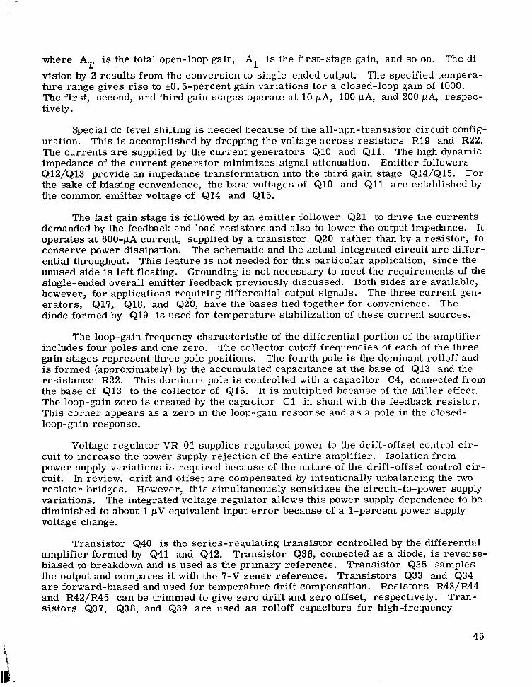
where AT is the total open-loop gain, A1 is the first-stage gain, and so on. The division by 2 results from the conversion to single-ended output. The specified temperature range gives r ise to 50.5-percent gain variations for a closed-loop gain of 1000. The first, second, and third gain stages operate at 10 PA, 100 PA, and 200 PA, respectively.
Special dc level shifting is needed because of the all-npn-transistor circuit configuration. This is accomplished by dropping the voltage across res is tors R19 and R22. The currents are supplied by the current generators QlO and Q11. The high dynamic impedance of the current generator minimizes signal attenuation. Emitter followers Q12/Q13 provide an impedance transformation into the third gain stage Q14/Q15. For the sake of biasing convenience, the base voltages of QlO and Q11 are established by the common emitter voltage of Q14 and Q15.
The last gain stage is followed by an emitter follower Q21 to drive the currents demanded by the feedback and load resis tors and also to lower the output impedance. It operates at 600-pA current, supplied by a transistor Q20 rather than by a resistor, to conserve power dissipation. The schematic and the actual integrated circuit a r e differential throughout. unused side is left floating. Grounding is not necessary to meet the requirements of the single-ended overall emitter feedback previously discussed.
This feature is not needed for this particular application, since the
Both sides a r e available, however, for applications requiring differential output signals. The three current generators, Q17, Q18, and Q20, have the bases tied together for convenience. The diode formed by Q19 is used for temperature stabilization of these current sources.
inc-ludes four poles and one zero. The loop-gain frequency characteristic of the differential portion of the amplifier
The collector cutoff frequencies of each of the three gain stages represent three pole positions. The fourth pole is the dominant rolloff and is formed (approximately) by the accumulated capacitance at the base of Q13 and the resistance R22. This dominant pole is controlled with a capacitor C4, connected from the base of Q13 to the collector of Q15. It is multiplied because of the Miller effect. The loop-gain zero is created by the capacitor C1 in shunt with the feedback resistor. This corner appears as a zero in the loop-gain response and as a pole in the closedloop-gain response.
Voltage regulator VR-01 supplies regulated power to the drift-offset control c i r cuit to increase the power supply rejection of the entire amplifier. Isolation from power supply variations is required because of the nature of the drift-offset control c i r cuit. In review, drift and offset are compensated by intentionally unbalancing the two resistor bridges. However, this simultaneously sensitizes the circuit-to-power supply variations. The integrated voltage regulator allows this power supply dependence to be diminished to about 1 pV equivalent input e r ro r because of a l-percent power supply voltage change.
Transistor Q40 is the series-regulating transistor controlled by the differential amplifier formed by Q41 and Q42. Transistor Q36, connected as a diode, is reverse-biased to breakdown and is used as the primary reference. Transistor Q35 samples the output and compares it with the 7-V zener reference. Transistors Q33 and Q34 a r e forward-biased and used for temperature drift compensation. Resistors R43/R44 and R42/R45 can be trimmed to give zero drift and zero offset, respectively. Transis tors Q37, Q38, and Q39 are used as rolloff capacitors for high-frequency
45

stabilization. A common transistor structure is used successfully as transistor, forward-biased diode, zener reference diode, and capacitor.
Voltage regulator VR-02 provides a precise +2.5-V reference potential with the following specifications: output voltage, +2.5 V *O. 1 percent with respect to ground; temperature stability, output *O. 1percent over -35" to +95" C range; line regulation,<io. 1percent output stability for *lo percent line variations through 100 kHz; output impedance, < 1 52; and operating current, 0 to 5 MA.
In this circuit, Q27 and Q28 a r e the series-regulating elements controlled by the Q29/Q30 differential amplifier. The zener reference is Q22, and Q32 is forward-biased to give temperature-drift compensation. A zener used to increase the regulation against positive input voltage changes is shown as Q31. Transistors Q23 through Q26 a r e used as rolloff capacitors. Adjustment of R40/R41 controls drift primarily, while R33/R34 controls offset. These resis tors can be adjusted to give the desired characteristic s.
Integration
The complete amplifier, including regulators, contains 135 components. Present fabrication yield necessitates dividing the circuit into separate integrable sections. The following eight modules were chosen on the basis of circuit function and equal complexity (fig. A-4):
Module type ~ ~.
Input
Output
Common mode
Drift-offset control
Drift-offset voltage regulator
Offset reference regulator
Feedback resistors
Capacitors
I
_ _
Components
Transistors and thin film resis tors
Thin film resis tors on silicon
Dielectric isolation metal on silicon capacitor
46

The first six modules are fabricated on a common-active substrate (MCD) containing 12 transistors and 4 diffused, crossunders. These MCD are converted to a unique circuit by depositing appropriate res is tors and aluminum interconnections. This approachallows stockpiling of wafers before circuit commitments a r e made, thereby significantly decreasing fabrication lead time and fabrication costs.
The minimum-geometry, buried-layer, epitaxial transistors (the smallest dimension is 0.25 mil) provide excellent high-frequency performance and maintain high current gains at very low current levels. Some pertinent characteristics are as follows:
Characteristic Typical value---_ dc current gain
I = 1mA, VCE = 2 V . . . . . . . . . . . . 150C
I c = l O p A , V C E = 2 V . . . . . . . . . . . 75
High-frequency current gain
f=lOOMHz, I = 3 m A . . . . . . . . . . 8 . 5C
I c = l m A . . . . . . . . . . 6 .5
IC= 100 pA . . . . . . . . . 2.0 IC = 10 P A . . . . . . . . . . 0.4
Collector- base capacitance
V C B = -2 V . . . . . . . . . . . . . . . 1.4 pF
Collector -substrate capacitance
Vcs= -10 V . . . . . . . . . . . . . . 2.2 pF
The resis tors are evaporated cermet thin-film structures with the following characteristics:
Width . . . . . . . . . . . . . . . . . . 0.5 mil Absolute tolerance . . . . . . . . . lt20 percent Ratio tolerance . . . . . . . . . . . . *1 percent Absolute temperature
coefficient . . . . . . . . . . . . 200 ppm/" c Ratio tracking temperature
coefficient . . . . . . . . . . . . . IO ppm/" c
47

Adjustment is accomplished by evaporating metal shorting links (by passing high current via probes) to increase a resistor value in binary related increments. The smallest actual resistance step is 150 Cn; however, within an appropriate res is tor network, this value is made to appear as low as an effective 5-0 step.
The capacitor module is fabricated with a new dielectric isolation technique whereby collector-substrate isolation is provided by an oxide insulation layer. This removes the dc leakages normally associated with the typical pn junction isolation. It also decreases the parasitic substrate capacitance to about 15 percent of the capacitor value, A thin layer of oxide is grown over an area of heavily doped N+ silicon. Aluminum is evaporated over the thin oxide. One capacitor plate is the aluminum and the other is the N+ silicon. Two sizes of capacitors are available on each module: a 75-pF type, adjustable in 5-pF steps; and a 15-pF type, adjustable in 1-pF steps. Each module contains a total of 480 pF.
The package layout is shown in figure A-5. Gain selection is made by connectingthe output to GlA, G2A, or G3A, and simultaneously making the corresponding ground connection to GlB, G2B, or G3B. A +2.5-V output offset is selected by replacing this ground connection with the +2.5-V connection. The package size is approximately 0.375 in. by 0.375 in. outside dimensions.
The integrated instrumentation amplifier described in this appendix yields drift characteristics which are competitive with high-performance chopper stabilized amplifiers. In addition, the gain, gain accuracy, and common-mode rejection characteristics make this amplifier an exceptionally useful microminiature building block for real- system applications.
48
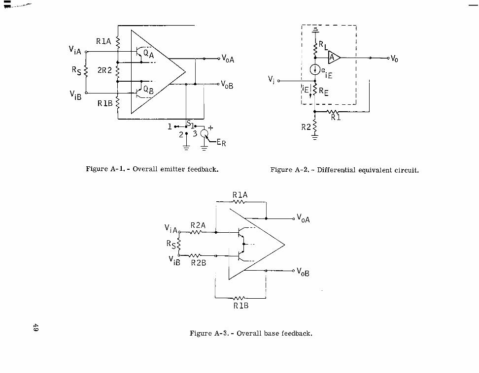
"iA
R S
"i B
I--:- - - - -7! T I
R2 P-Figure A-2. - Differential equivalent circuit.Figure A- 1. - Overall emitter feedback.
-R LA
o voA
"iB R2B -vo B
LR/Lr
I? 16
Figure A-3. - Overall base feedback. cpW
I
I ..-
F E E D B A C K RESISTORS
RA-01
, I
Figure A-4. - Complete amplifier.
I

INPUT G 1 A G 2 A G 3 A INA GRD OUT -9
G 1B G 2 B G 3 B IN B P S +2.5 +9 GRD
Figure A-5. - Package layout.
51

APPENDIX B
SPECIFICATIONS FOR A MICROMINIATURE dc AMPLIFIER
Scope
This specification covers one type of signal-conditioning module.
Applicable Documents
Interference Control Requirements, MIL-1-26600.
Requirements
Materials. - Except as specified herein, the selection of materials shall be the opt ion%Tthent rac tor .
Design. - The module shall be designed to condition signals from sensors o r similar devices to a level of 0 to +5 V for telemetering space program signals.
Construction. - Except as specified herein, the methods and techniques of construction shall be at the option of the contractor. The module shall be in a rectilinear configuration with weldable and solderable leads brought out in one plane.
Environmental specifications. - The module shall operate within the electrical specifications for any combination of the following environmental conditions.
Supply voltage conditions: The nominal voltage and current is to be selected by the contractor. This voltage may vary by rt5 percent over a frequency range of from dc to 100 kc.
Radio-frequency interference: The module shall meet Specification MIL-1-26600.
Temperature range: The module shall start and operate at any constant o r variable (20" F/min maximum) temperature from -30" to +200" F. The module shall not be damaged when subjected to a nonoperating storage of at least 6 hours at any temperature from -65" to +250° F.
Service life: The module shall be capable of operating for a minimum of 2000 hours, continuously or otherwise, during a service life of 1 year.
Warmup time: The module shall be capable of operation with a warmup time not to exceed 50 psec.
Electrical specifications. - The module shall operate within the following specificationswhen subjected to the environments specified.
53

Input signal: The module shall be capable of receiving variable differential input signals of from 0 to lt5 V without damage.
Input impedance: The input impedance shall be 50 k52 o r greater for any gain setting and for any frequency from dc to 5000 cps. A back current, not exceeding 0 . 2 PA, shall be supplied internally to accommodate a floating source.
Output bias and offset: With a zero input signal from a floating source impedance of from 0 to 375 51, the module output shall be capable of being set to 0 o r 2 . 5 V. Selection shall be by moving jumper wires between external leads. This output voltage shall be within *50 mV of the ideal value over the environment range specified.
Output signal: The module shall be capable of delivering output signals of from 0 to +5 V with the output bias set at either 0 o r +2.5 V to a load of 50 kS2 to open circuit.
Output impedance: The output impedance of the module shall not exceed 100 52 from dc to 5000 cps.
Voltage gain: The voltage gain shall be adjustable in steps within 1 percent of the ideal values of 700, 850, and 1000. This adjustment shall consist of jumper wires connected between identified leads. No components shall be added to change from one gain setting to another.
Gain stability and frequency response: The gain of the module shall be within *1 percent of the dc value at 75" F from dc to 5000 cps. The frequency response shall not change more than *1 percent over the specified environment range.
Output ripple: The maximum output ripple voltage shall be 25 mV peak to peak from dc through 15 mHz with 90-percent confidence level measured over a period of 1 second.
Linearity: The module shall have a linear output with rt12.5 mV of a straight line between the end points (nominal 0 and +5 V) with the output bias set at either 0 o r +2.5 v.
Grounding procedure: The signal input shall be of the differential type and shall accommodate a floating source. No external input ground reference shall be needed.
Common mode: The module shall have a common mode rejection ratio of 80 dB o r more for a 0- to 375-52 floating source resistance for frequencies from dc to 5000 cps and for voltages of 4.0 V.
Mechanical mecifications. -Volume: The module volume shall be 0.01 cu in. o r less.
Color: The module case shall be opaque.
54

Product marking: The module and all external leads shall be marked for identification purposes in a permanent manner.
Workmanship: Uniformity of shapes, dimensions, and performances shall pro -vide interchangeability of the complete module. There shall be no cracks, breaks, dents, or any other defects.
55

RE FERE NCES
1. Middlebrook, R. D. : Differential Amplifiers: Their Analysis and Their Applications in Transistor d. c. Amplifiers. John Wiley and Sons, Inc., 1963.
2. Middlebrook, R. D. : Design-Oriented Analysis of Feedback Amplifiers. Paper presented at National Electronics Conference (Chicago, Ill. ), Oct. 1964.
3. Middlebrook, R. D. ;and Taylor, A. D. : Differential Amplifier with Regulator Achieves High Stability, Low Drift. Electronics, vol. 34, no. 30, July 1961, pp. 56-59.
4. Hoffait, A. H. ;and Thornton, R. D. : Limitations of Transistor DC Amplifiers. Proc. IEEE, vol. 52, no. 2, Feb. 1964, pp. 179-184.
5. Tuszynski, A. : Correlation Between Base-Emitter Voltage and its Temperature Coefficient. Solid State Design, vol. 3, no. 7, July 1962, pp. 32-35.
56 NASA-Langley, 1967 -9 s-125

“The aeronautical and space activities of the United States shall be conducted so a.r to contribute . . . to the expanrion of human Rnowledge of phenomena in the atmo.rphere and space. The Adminijtration shall provide for the widest practicable and appropriate dissemination of information concerning its activities and the results tbereof.”
-NATIONALAERONAUTICS AND SPACE ACT OF 1958
NASA SCIENTIFIC AND TECHNICAL PUBLICATIONS
TECHNICAL REPORTS: Scientific and technical information considered important, complete, and a lasting contribution to existing knowle(lge.
TECHNICAL NOTES: Information less broad in scope but nevertheless of importance as a contribution to existing knowledge.
TECHNICAL MEMORANDUMS: Information receiving limited distributionbecause of preliminary data, security classification,or other reasons.
CONTRACTOR REPORTS: Scientific and technical information generated under a NASA contract or grant and considered an important contribution to existing knowledge.
TECHNICAL TRANSLATIONS: Information published in a foreign language considered to merit NASA distribution in English.
SPECIAL PUBLICATIONS: Information derived from or of value to NASA activities. Publications include conference proceedings, monographs, data compilations, handbooks, sourcebooks, and special bibliographies.
TECHNOLOGY UTILIZATION PUBLICATIONS: Information on technology used by NASA that may be of particular interest in commercial and other non-aerospace applications. Publications include Tech Briefs, Technology Utilization Reports and Notes, and Technology Surveys.
Details on the availability of these publications may be obtained from:
SCIENTIFIC AND TECHNICAL INFORMATION DIVISION
AL AERONAUTICSAND SPACE ADMINISTRATION
Washington, D.C. PO546