Embed Size (px)
Citation preview
The effect of Zn vacancies and Ga dopants on the
electronic structure of ZnO: Ab initio simulations
Alexandre V Sorokin1, Yuri F Zhukovskii, Juris Purans andEugene A Kotomin
Institute for Solid State Physics, University of Latvia, 8 Kengaraga Str., Riga, LV-1063, Latvia
E-mail: [email protected]
Abstract. Zinc oxide modified by metal dopants can be used as a low-cost material forproduction of transparent conducting films. Its optical and electronic properties vary withthe type and the concentration of dopants. In this study we have performed first-principlecalculations on ZnO with Zn vacancies and that with Ga dopants in wurtzite type hexagonalmorphology using density functional theory approach. Dependence of the electronic propertieson the concentration of dopants has been studied using supercells of different sizes.
1. IntroductionZnO continues to attract enhanced technological interest as a suitable material for manufacturingof transparent conducting films for electrodes and other microelectronic applications. The wideaccessibility of ZnO single crystals [1] make ZnO a promising low-cost material for synthesis ofnanostructures with a large variety of morphologies and for substrates. Under normal conditionsZnO exists in the wurzite-type hexagonal polymorph, being a wide-gap semiconductor with aband gap Eg = 3.4 eV [2, 3]). When ZnO is doped by Ga, Al or transition metal atoms,its electrical conductivity increases retaining high optical transparency. Doped ZnO can beconsidered as a good substitute for indium–tin oxide in manufacturing of transparent electrodes[1]. Fabrication of doped and undoped ZnO thin films is accompanied by formation of O andZn vacancies and interstitials [4] and formation of nitrogen complexes [4], as well as hydrogenadsorption [5], which contributes to n-type conductivity.
In recent years energetics of formation of O and Zn vacancies and interstitials was calculatedusing hybrid QM/MM approach [3, 6], DFT-PAW approach with semi-local GGA [7] andLDA/GGA parametrization [8]. Acting as deep acceptors or deep donors, no intrinsic defectscan cause conductivity [9]. In contrast, adsorbed hydrogen is readily incorporated as an H+
interstitial, ensuring n-type conductivity [9]. Sokol et al [6] have shown that metal atom dopantsusually act as deep donors, reluctantly taking part in the formation of conductivity.
In this study we have performed first-principles calculations on the atomic and electronicstructure of pure and doped ZnO with different concentrations of defects in order to analyze theeffect of Ga dopant and VZn on different properties.
2. Computational details & preliminary calculationsDFT calculations have been performed using basis sets of linear combination of atomic orbitals(LCAO) combined with hybrid DFT-HF exchange–correlation functional PBE0 as implemented
1 Corresponding author
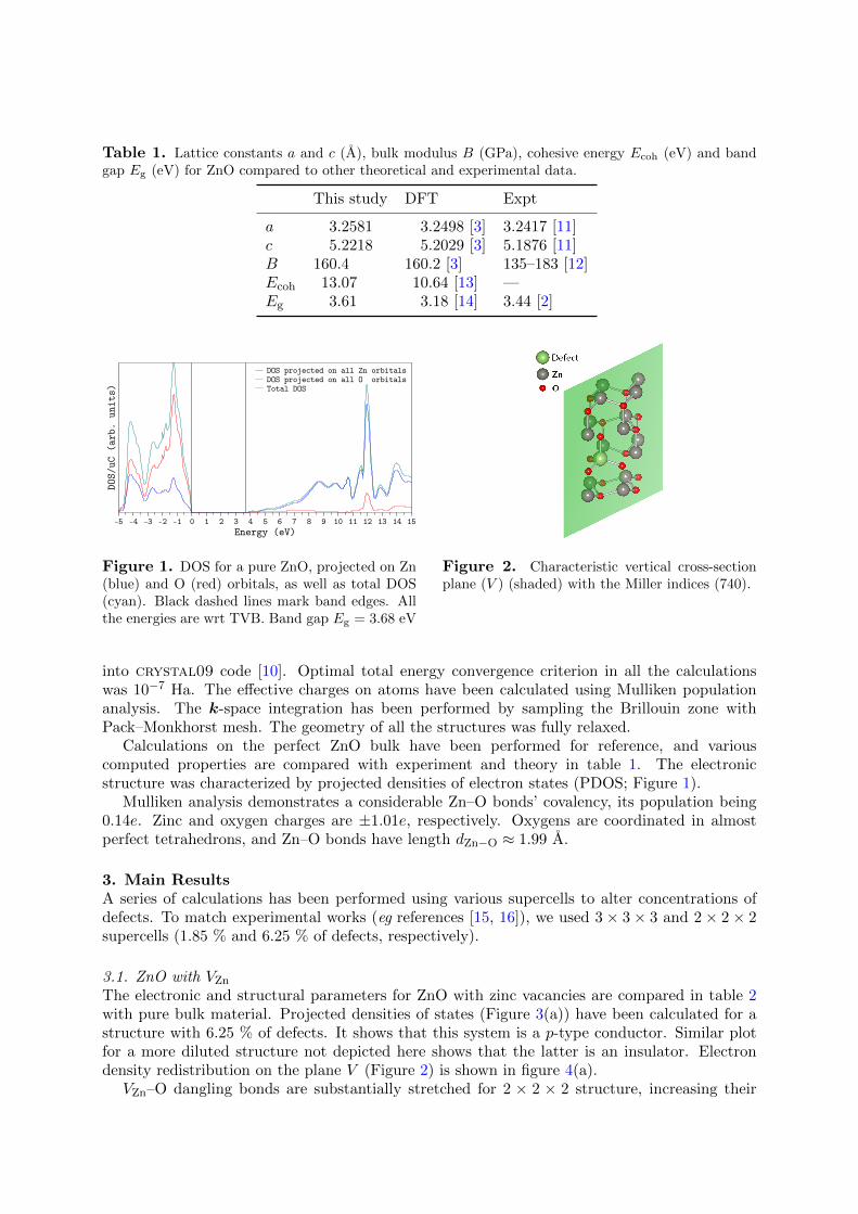
Table 1. Lattice constants a and c (A), bulk modulus B (GPa), cohesive energy Ecoh (eV) and bandgap Eg (eV) for ZnO compared to other theoretical and experimental data.
This study DFT Expt
a 3.2581 3.2498 [3] 3.2417 [11]c 5.2218 5.2029 [3] 5.1876 [11]B 160.4 160.2 [3] 135–183 [12]Ecoh 13.07 10.64 [13] —Eg 3.61 3.18 [14] 3.44 [2]
DOS/
uC (
arb.
uni
ts)
Energy (eV)-5 -4 -3 -2 -1 0 1 2 3 4 5 6 7 8 9 10 11 12 13 14 15
DOS projected on all Zn orbitalsDOS projected on all O orbitalsTotal DOS
Figure 1. DOS for a pure ZnO, projected on Zn(blue) and O (red) orbitals, as well as total DOS(cyan). Black dashed lines mark band edges. Allthe energies are wrt TVB. Band gap Eg = 3.68 eV
Figure 2. Characteristic vertical cross-sectionplane (V ) (shaded) with the Miller indices (740).
into crystal09 code [10]. Optimal total energy convergence criterion in all the calculationswas 10−7 Ha. The effective charges on atoms have been calculated using Mulliken populationanalysis. The k-space integration has been performed by sampling the Brillouin zone withPack–Monkhorst mesh. The geometry of all the structures was fully relaxed.
Calculations on the perfect ZnO bulk have been performed for reference, and variouscomputed properties are compared with experiment and theory in table 1. The electronicstructure was characterized by projected densities of electron states (PDOS; Figure 1).
Mulliken analysis demonstrates a considerable Zn–O bonds’ covalency, its population being0.14e. Zinc and oxygen charges are ±1.01e, respectively. Oxygens are coordinated in almostperfect tetrahedrons, and Zn–O bonds have length dZn−O ≈ 1.99 A.
3. Main ResultsA series of calculations has been performed using various supercells to alter concentrations ofdefects. To match experimental works (eg references [15, 16]), we used 3 × 3 × 3 and 2 × 2 × 2supercells (1.85 % and 6.25 % of defects, respectively).
3.1. ZnO with VZn
The electronic and structural parameters for ZnO with zinc vacancies are compared in table 2with pure bulk material. Projected densities of states (Figure 3(a)) have been calculated for astructure with 6.25 % of defects. It shows that this system is a p-type conductor. Similar plotfor a more diluted structure not depicted here shows that the latter is an insulator. Electrondensity redistribution on the plane V (Figure 2) is shown in figure 4(a).
VZn–O dangling bonds are substantially stretched for 2 × 2 × 2 structure, increasing their
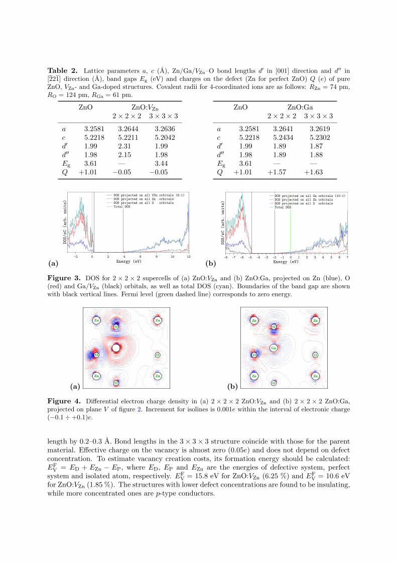
Table 2. Lattice parameters a, c (A), Zn/Ga/VZn–O bond lengths d′ in [001] direction and d′′ in[221] direction (A), band gaps Eg (eV) and charges on the defect (Zn for perfect ZnO) Q (e) of pureZnO, VZn- and Ga-doped structures. Covalent radii for 4-coordinated ions are as follows: RZn = 74 pm,RO = 124 pm, RGa = 61 pm.
ZnO ZnO:VZn
2 × 2 × 2 3 × 3 × 3
a 3.2581 3.2644 3.2636c 5.2218 5.2211 5.2042d′ 1.99 2.31 1.99d′′ 1.98 2.15 1.98Eg 3.61 — 3.44Q +1.01 −0.05 −0.05
ZnO ZnO:Ga2 × 2 × 2 3 × 3 × 3
a 3.2581 3.2641 3.2619c 5.2218 5.2434 5.2302d′ 1.99 1.89 1.87d′′ 1.98 1.89 1.88Eg 3.61 — —Q +1.01 +1.57 +1.63
(a)
DOS/
sC (
arb.
uni
ts)
Energy (eV)−2 0 2 4 6 8 10 12
DOS projected on all VZn orbitals (8:1)DOS projected on all Zn orbitalsDOS projected on all O orbitalsTotal DOS
(b)
DOS/
sC (
arb.
uni
ts)
Energy (eV)-8 -7 -6 -5 -4 -3 -2 -1 0 1 2 3 4 5 6 7
DOS projected on all Ga orbitals (10:1)DOS projected on all Zn orbitalsDOS projected on all O orbitalsTotal DOS
Figure 3. DOS for 2 × 2 × 2 supercells of (a) ZnO:VZn and (b) ZnO:Ga, projected on Zn (blue), O(red) and Ga/VZn (black) orbitals, as well as total DOS (cyan). Boundaries of the band gap are shownwith black vertical lines. Fermi level (green dashed line) corresponds to zero energy.
(a)
Zn
O
Zn
O
O
Zn Zn
O(b)
Zn
O
Zn
O
Ga
O
Zn Zn
O
Figure 4. Differential electron charge density in (a) 2 × 2 × 2 ZnO:VZn and (b) 2 × 2 × 2 ZnO:Ga,projected on plane V of figure 2. Increment for isolines is 0.001e within the interval of electronic charge(−0.1 ÷ +0.1)e.
length by 0.2–0.3 A. Bond lengths in the 3 × 3 × 3 structure coincide with those for the parentmaterial. Effective charge on the vacancy is almost zero (0.05e) and does not depend on defectconcentration. To estimate vacancy creation costs, its formation energy should be calculated:EF
V = ED + EZn − EP, where ED, EP and EZn are the energies of defective system, perfectsystem and isolated atom, respectively. EF
V = 15.8 eV for ZnO:VZn (6.25 %) and EFV = 10.6 eV
for ZnO:VZn (1.85 %). The structures with lower defect concentrations are found to be insulating,while more concentrated ones are p-type conductors.
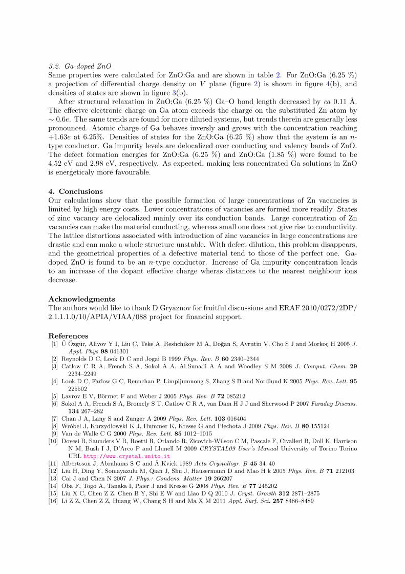
3.2. Ga-doped ZnOSame properties were calculated for ZnO:Ga and are shown in table 2. For ZnO:Ga (6.25 %)a projection of differential charge density on V plane (figure 2) is shown in figure 4(b), anddensities of states are shown in figure 3(b).
After structural relaxation in ZnO:Ga (6.25 %) Ga–O bond length decreased by ca 0.11 A.The effectve electronic charge on Ga atom exceeds the charge on the substituted Zn atom by∼ 0.6e. The same trends are found for more diluted systems, but trends therein are generally lesspronounced. Atomic charge of Ga behaves inversly and grows with the concentration reaching+1.63e at 6.25%. Densities of states for the ZnO:Ga (6.25 %) show that the system is an n-type conductor. Ga impurity levels are delocalized over conducting and valency bands of ZnO.The defect formation energies for ZnO:Ga (6.25 %) and ZnO:Ga (1.85 %) were found to be4.52 eV and 2.98 eV, respectively. As expected, making less concentrated Ga solutions in ZnOis energeticaly more favourable.
4. ConclusionsOur calculations show that the possible formation of large concentrations of Zn vacancies islimited by high energy costs. Lower concentrations of vacancies are formed more readily. Statesof zinc vacancy are delocalized mainly over its conduction bands. Large concentration of Znvacancies can make the material conducting, whereas small one does not give rise to conductivity.The lattice distortions associated with introduction of zinc vacancies in large concentrations aredrastic and can make a whole structure unstable. With defect dilution, this problem disappears,and the geometrical properties of a defective material tend to those of the perfect one. Ga-doped ZnO is found to be an n-type conductor. Increase of Ga impurity concentration leadsto an increase of the dopant effective charge wheras distances to the nearest neighbour ionsdecrease.
AcknowledgmentsThe authors would like to thank D Gryaznov for fruitful discussions and ERAF 2010/0272/2DP/2.1.1.1.0/10/APIA/VIAA/088 project for financial support.
References[1] U Ozgur, Alivov Y I, Liu C, Teke A, Reshchikov M A, Dogan S, Avrutin V, Cho S J and Morkoc H 2005 J.
Appl. Phys 98 041301[2] Reynolds D C, Look D C and Jogai B 1999 Phys. Rev. B 60 2340–2344[3] Catlow C R A, French S A, Sokol A A, Al-Sunadi A A and Woodley S M 2008 J. Comput. Chem. 29
2234–2249[4] Look D C, Farlow G C, Reunchan P, Limpijumnong S, Zhang S B and Nordlund K 2005 Phys. Rev. Lett. 95
225502[5] Lavrov E V, Borrnet F and Weber J 2005 Phys. Rev. B 72 085212[6] Sokol A A, French S A, Bromely S T, Catlow C R A, van Dam H J J and Sherwood P 2007 Faraday Discuss.
134 267–282[7] Chan J A, Lany S and Zunger A 2009 Phys. Rev. Lett. 103 016404[8] Wrobel J, Kurzyd lowski K J, Hummer K, Kresse G and Piechota J 2009 Phys. Rev. B 80 155124[9] Van de Walle C G 2000 Phys. Rev. Lett. 85 1012–1015
[10] Dovesi R, Saunders V R, Roetti R, Orlando R, Zicovich-Wilson C M, Pascale F, Civalleri B, Doll K, HarrisonN M, Bush I J, D’Arco P and Llunell M 2009 CRYSTAL09 User’s Manual University of Torino TorinoURL http://www.crystal.unito.it
[11] Albertsson J, Abrahams S C and A Kvick 1989 Acta Crystallogr. B 45 34–40[12] Liu H, Ding Y, Somayazulu M, Qian J, Shu J, Hausermann D and Mao H k 2005 Phys. Rev. B 71 212103[13] Cai J and Chen N 2007 J. Phys.: Condens. Matter 19 266207[14] Oba F, Togo A, Tanaka I, Paier J and Kresse G 2008 Phys. Rev. B 77 245202[15] Liu X C, Chen Z Z, Chen B Y, Shi E W and Liao D Q 2010 J. Cryst. Growth 312 2871–2875[16] Li Z Z, Chen Z Z, Huang W, Chang S H and Ma X M 2011 Appl. Surf. Sci. 257 8486–8489