Embed Size (px)
Citation preview

2
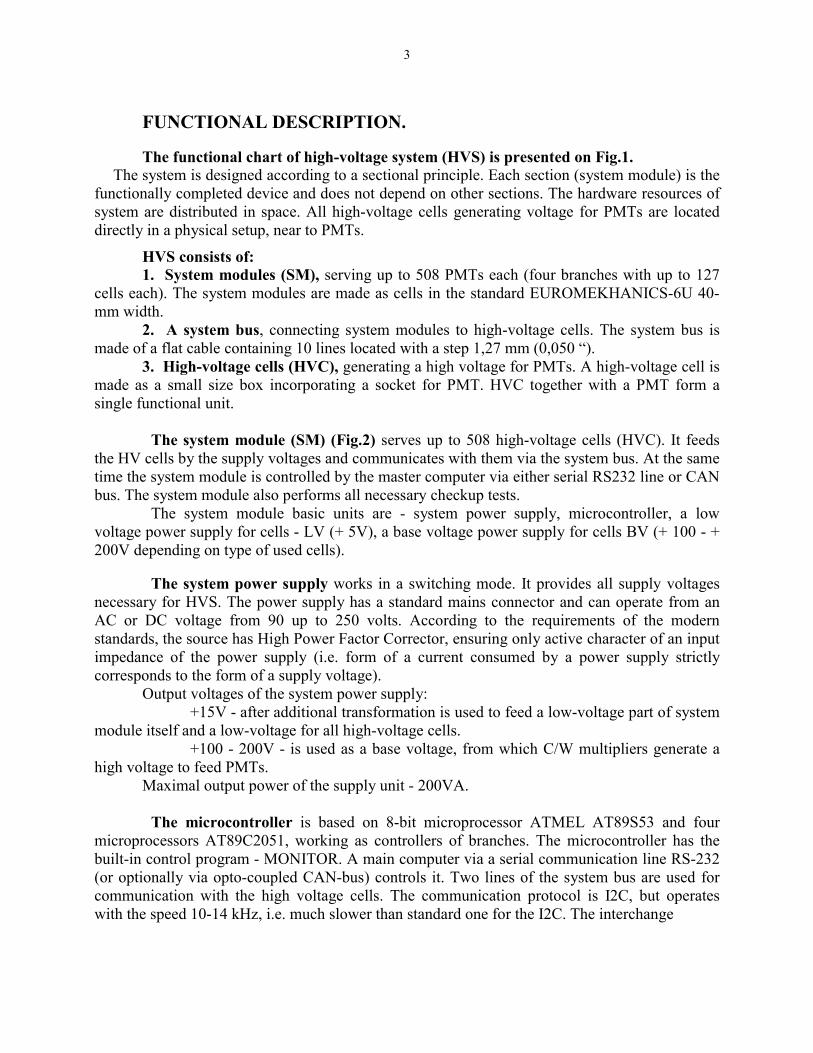
The High Voltage System (HVS) provides the powering of largearrays of PMT’s (10 -102 4 ) in large-scale physical experiments.
The basic conceptual ideas of the system:
♦♦♦♦ generation of a high voltage directly in a place of its consumption;♦♦♦♦ use Cockroft-Walton multipliers for generation of a high voltage;♦♦♦♦ absence of expensive high-voltage cables and connectors.
Main features of the system:
♦♦♦♦ FULL COMPLETED FUNCTIONAL DEVICE;
♦♦♦♦ HIGH DENSITY, UP TO 508 CHANNELS PER SYSTEM MODULE;
♦♦♦♦ ABSENCE OF HIGH-VOLTAGE CABLES AND CONNECTORS;
♦♦♦♦ OWN POWER DISSIPATION LESS THAN 0,05 W/channel;
♦♦♦♦ HIGH STABILITY OF OUTPUT VOLTAGES - 0,05 %;
♦♦♦♦ REMOTE CONTROL OF ALL CHANNELS;
♦♦♦♦ PMT PROTECTION AGAINST CURRENT OVERLOAD;
♦ COMPUTER CONTROL VIA SERIAL RS232 LINE OR OPTIONALLYVIA CAN bus.
3
FUNCTIONAL DESCRIPTION.
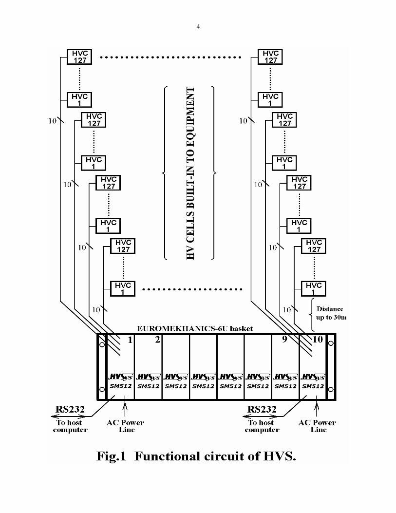
The functional chart of high-voltage system (HVS) is presented on Fig.1.The system is designed according to a sectional principle. Each section (system module) is the
functionally completed device and does not depend on other sections. The hardware resources ofsystem are distributed in space. All high-voltage cells generating voltage for PMTs are locateddirectly in a physical setup, near to PMTs.
HVS consists of:1. System modules (SM), serving up to 508 PMTs each (four branches with up to 127
cells each). The system modules are made as cells in the standard EUROMEKHANICS-6U 40-mm width.
2. A system bus, connecting system modules to high-voltage cells. The system bus ismade of a flat cable containing 10 lines located with a step 1,27 mm (0,050 “).
3. High-voltage cells (HVC), generating a high voltage for PMTs. A high-voltage cell ismade as a small size box incorporating a socket for PMT. HVC together with a PMT form asingle functional unit.
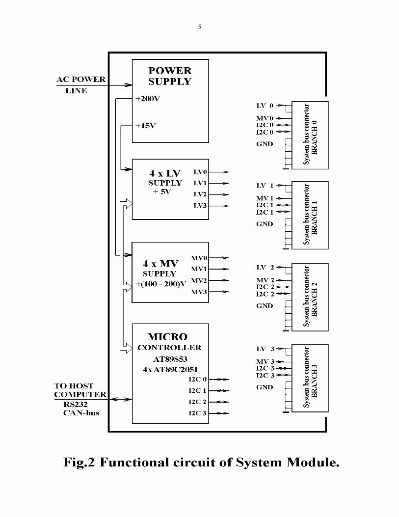
The system module (SM) (Fig.2) serves up to 508 high-voltage cells (HVC). It feedsthe HV cells by the supply voltages and communicates with them via the system bus. At the sametime the system module is controlled by the master computer via either serial RS232 line or CANbus. The system module also performs all necessary checkup tests.
The system module basic units are - system power supply, microcontroller, a lowvoltage power supply for cells - LV (+ 5V), a base voltage power supply for cells BV (+ 100 - +200V depending on type of used cells).
The system power supply works in a switching mode. It provides all supply voltagesnecessary for HVS. The power supply has a standard mains connector and can operate from anAC or DC voltage from 90 up to 250 volts. According to the requirements of the modernstandards, the source has High Power Factor Corrector, ensuring only active character of an inputimpedance of the power supply (i.e. form of a current consumed by a power supply strictlycorresponds to the form of a supply voltage).
Output voltages of the system power supply:+15V - after additional transformation is used to feed a low-voltage part of system
module itself and a low-voltage for all high-voltage cells.+100 - 200V - is used as a base voltage, from which C/W multipliers generate a
high voltage to feed PMTs.Maximal output power of the supply unit - 200VA.
The microcontroller is based on 8-bit microprocessor ATMEL AT89S53 and fourmicroprocessors AT89C2051, working as controllers of branches. The microcontroller has thebuilt-in control program - MONITOR. A main computer via a serial communication line RS-232(or optionally via opto-coupled CAN-bus) controls it. Two lines of the system bus are used forcommunication with the high voltage cells. The communication protocol is I2C, but operateswith the speed 10-14 kHz, i.e. much slower than standard one for the I2C. The interchange
4
5
6
protocol is realized by the software of the AT89C2051 branch controller in a master regime. Eachbranch has its own branch controller. All cells (HVC) operate as slaves on the branch.
The microcontroller also controls the power supplies LV and BV, checks them andprovide an emergency protection. For the checkup of power supplies voltages 8-bit 8-channelanalog to digital converter presents in its structure.
The LV bus source (+5V) generates a low voltage for the system bus. Each branch hasits own LV source, which can be switched on and off independently. Every LV supply line (+5V)has an electronic protection against a current overload (threshold current of 1,0А) and a fuse.
The BV bus source (100 - 200V) generates a base voltage for the system bus. Thesource has four channels, which can be switched on/off independently. The source guarantied asmooth rise of a voltage and fast shutting off by special hardware circuits. Besides it provide anindependent protection of BV lines against a short circuit. This protection has two levels. Whenthe current in a line exceeds the threshold of 0,3А the BV source switches to a constant currentmode. The microcontroller periodically once in 4 seconds checks an output BV voltage of thesources. If it doesn’t correspond to expected value, the microcontroller switches off the powersupply of a faulty branch. Additionally every branch has a fuse.
The system bus connects all high-voltage cells (HVC) of the given branch to theappropriate channel of system module (SM). All HVC of one branch are connected in parallel.The system module has on the front panel 40-pins connector for connection of four system busbranches.
Functional assignment of the bus lines:♦ two lines LV (+5V) - supply of low-voltage part of HVC;♦ one line BV (100-200V) - base HVC voltage;♦ five ground lines (GND);♦ two lines for serial communication interface:
♦ SCL - synchronization;♦ SDA - address, data.
The high-voltage cell HVC (Fig. 3) accepts commands from the system bus andexecutes them i.e. sets the high voltage, switch it on and off, checks the status etc. HVC isfunctionally divided into two units - driver and C/W voltage multiplier. Each unit is located onseparate printed-circuit board.
The driver is constructed on the basis of the microcontroller PIC12C509 and 10-bitdigital-to-analog converter LTC1661. Every HVC has internal 7-bit address. This address mustbe unique within one branch. HVC accepts commands addressed to it and execute them. Datawritten to the DAC controls the operation of the pumping driver. This driver generates a variablevoltage of the rectangular form of amplitude 0 - BV and frequency about 10 kHz. This signal isused for pumping of the high-voltage multiplier. The high voltage of each cell can be switched onand off simultaneously. The pumping driver has a dedicated control input for this purpose.
The output voltage of HVC is stabilized by a feedback loop formed by a divider Rfb/Ro,inverting amplifier A1 and amplifier of an error signal A2. Due to the built - in source of
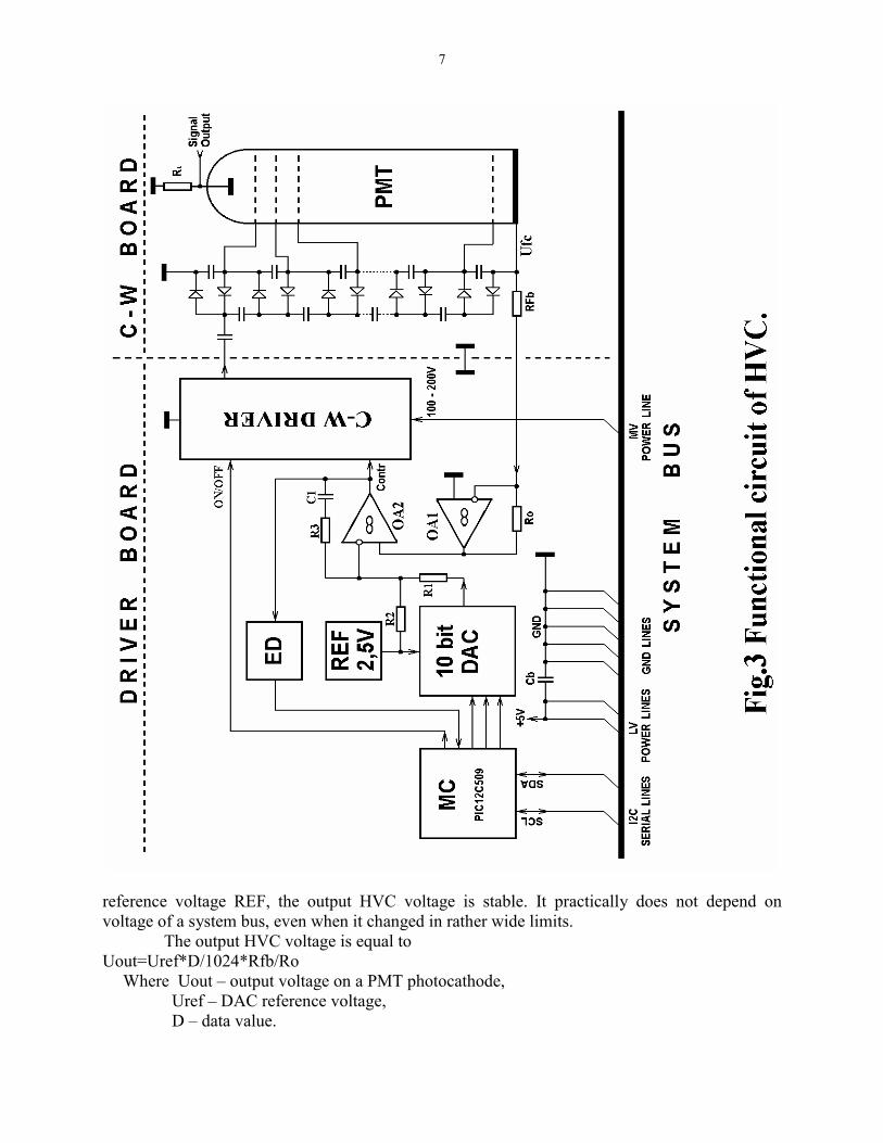
7
reference voltage REF, the output HVC voltage is stable. It practically does not depend onvoltage of a system bus, even when it changed in rather wide limits.
The output HVC voltage is equal toUout=Uref*D/1024*Rfb/Ro
Where Uout – output voltage on a PMT photocathode, Uref – DAC reference voltage, D – data value.
8
The voltage multiplier driver has the output current restriction circuit. This measureallows to limit an maximal average anode PMT current to protects a PMT against currentoverload.
The control of HVC operation is performed according to the value of an error signal onthe output of the amplifier A2. The cell has an error detection circuit. The microcontroller of acell checks an error detection circuit output every 25 milliseconds. If an error condition appearseven for a short time, it stored in a status register in "accumulated error" bit. Later system modulewill read the status register and report the error.
The high voltage multiplier (Fig. 3) - Cockroft-Walton voltage multiplier works by aprinciple of the charging pump. On the multiplier board residues the voltage multiplier itself,elements suppressing pulsation and high-resistance resistor of a feedback loop Rfb. Every dynodeinterval of a PMT is being fed from one or several steps of the voltage multiplier. The schematic and topology of the multiplier board can be slightly different depending ontype of used PMT. For protection against high-voltage discharges and atmospheric moistureinfluence the multiplier board is covered by protective layer of silicon compound.
THE OPERATIONAL DESCRIPTION.
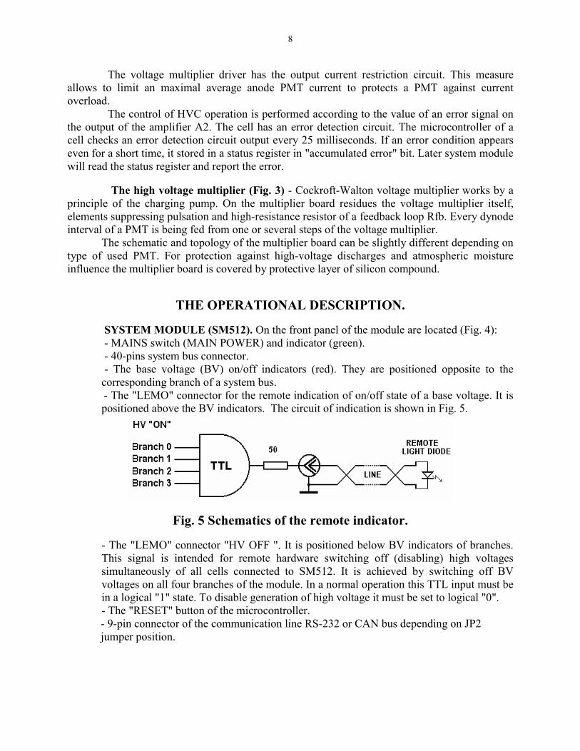
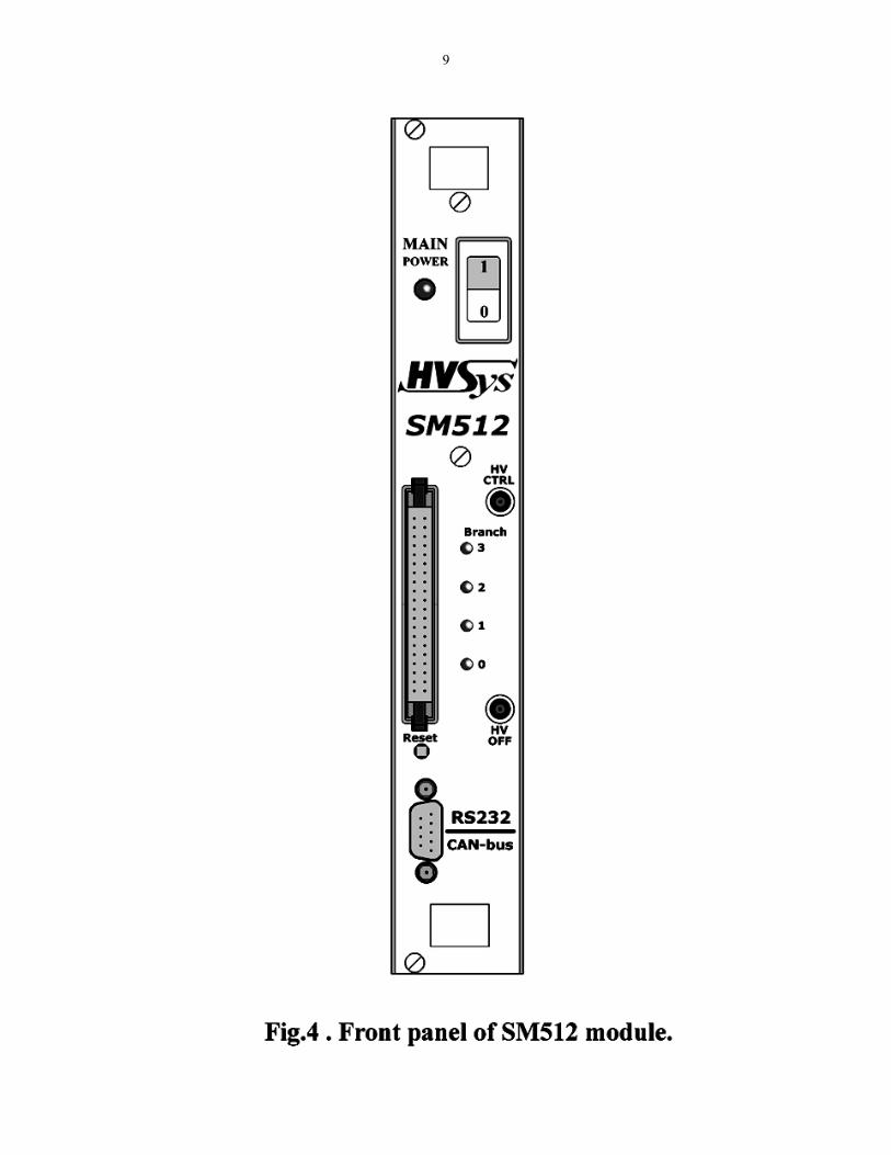
SYSTEM MODULE (SM512). On the front panel of the module are located (Fig. 4): - MAINS switch (MAIN POWER) and indicator (green). - 40-pins system bus connector. - The base voltage (BV) on/off indicators (red). They are positioned opposite to thecorresponding branch of a system bus.- The "LEMO" connector for the remote indication of on/off state of a base voltage. It ispositioned above the BV indicators. The circuit of indication is shown in Fig. 5.
Fig. 5 Schematics of the remote indicator.
- The "LEMO" connector "HV OFF ". It is positioned below BV indicators of branches.This signal is intended for remote hardware switching off (disabling) high voltagessimultaneously of all cells connected to SM512. It is achieved by switching off BVvoltages on all four branches of the module. In a normal operation this TTL input must bein a logical "1" state. To disable generation of high voltage it must be set to logical "0".- The "RESET" button of the microcontroller.- 9-pin connector of the communication line RS-232 or CAN bus depending on JP2jumper position.
9
10
In addition to the external RS232 connector there is also internal one. This internal RS232connector can be used for service purposes when external connector configured/used as CAN bus
connector.The pinouts of the RS232 connectors are presented in table 1.
Table 1.Name RXD TXD GND
External connector Pin № 2 3 5Internal connector (P2) Pin № 2 3 4
The pinout of the CAN bus connector is presented in table 2.Table 2.
Name SHILD Us (-12V) CANL CANH Uc (+12V)Pin № 3 6 7 8 9
Us and Uc lines are dedicated for internal optocoupler supply. These two voltages mustbe provided from external controller. These voltages should be in 9-15 Volt limits.
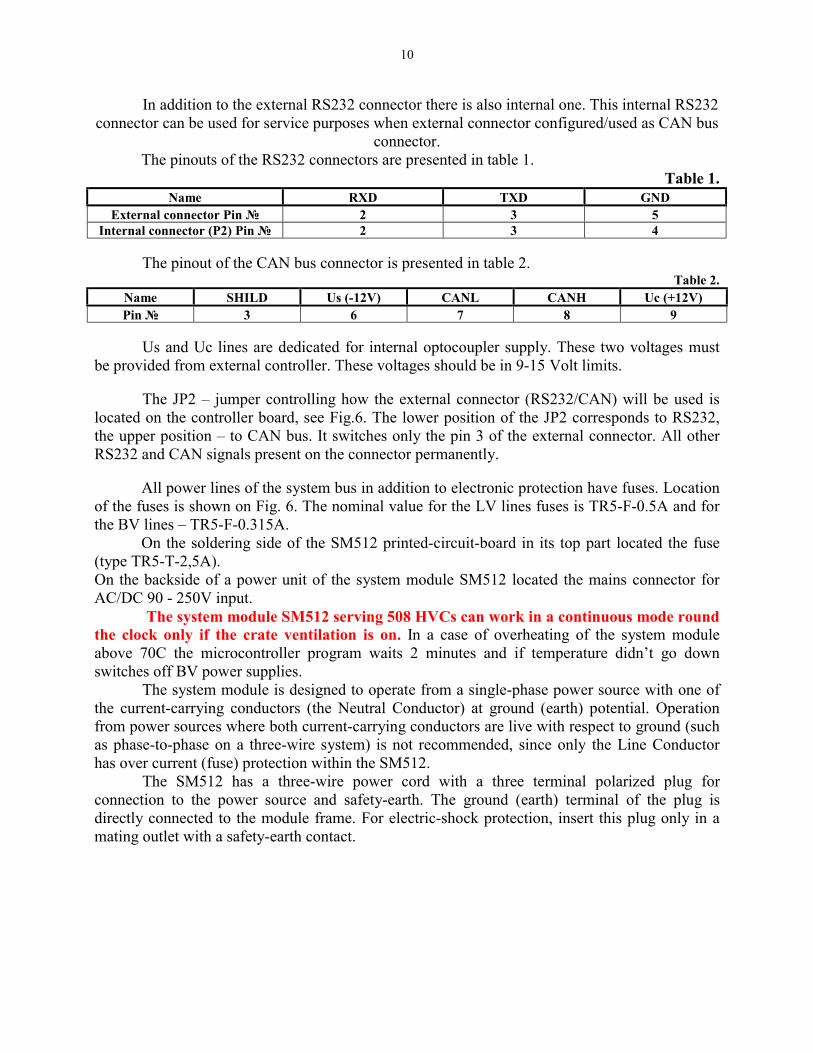
The JP2 – jumper controlling how the external connector (RS232/CAN) will be used islocated on the controller board, see Fig.6. The lower position of the JP2 corresponds to RS232,the upper position – to CAN bus. It switches only the pin 3 of the external connector. All otherRS232 and CAN signals present on the connector permanently.
All power lines of the system bus in addition to electronic protection have fuses. Locationof the fuses is shown on Fig. 6. The nominal value for the LV lines fuses is TR5-F-0.5A and forthe BV lines – TR5-F-0.315A.
On the soldering side of the SM512 printed-circuit-board in its top part located the fuse(type TR5-T-2,5А).On the backside of a power unit of the system module SM512 located the mains connector forAC/DC 90 - 250V input.
The system module SM512 serving 508 HVCs can work in a continuous mode roundthe clock only if the crate ventilation is on. In a case of overheating of the system moduleabove 70C the microcontroller program waits 2 minutes and if temperature didn’t go downswitches off BV power supplies.
The system module is designed to operate from a single-phase power source with one ofthe current-carrying conductors (the Neutral Conductor) at ground (earth) potential. Operationfrom power sources where both current-carrying conductors are live with respect to ground (suchas phase-to-phase on a three-wire system) is not recommended, since only the Line Conductorhas over current (fuse) protection within the SM512.
The SM512 has a three-wire power cord with a three terminal polarized plug forconnection to the power source and safety-earth. The ground (earth) terminal of the plug isdirectly connected to the module frame. For electric-shock protection, insert this plug only in amating outlet with a safety-earth contact.
11
12
SYSTEM BUS. Numbers of connector pins/lines of a system bus and their assignmentare given in the Table 3:
Table 3.LINE LV GND LV GND SCL GND SDA GND BV GND
Branch 0 1 2 3 4 5 6 7 8 9 10Branch 1 11 12 13 14 15 16 17 18 19 20Branch 2 21 22 23 24 25 26 27 28 29 30Branch 3 31 32 33 34 35 36 37 38 39 40
For manufacture of the system bus the flat cable with heightened wires cross section(0.13 sq. mm) is used. For example Belden 9L26010, gray ribbon cable, 0.050 " Pitch, 26AWG, 10 Conductors. At full branch load - 127 cells, maximum length of a cable should notexceed 30 m. After manufacturing a cable of the system bus it must be checked for a short circuitbetween the wires. Maximal length of a cable depends on an amount and type of HV cells used,their allocations on a branch and in some cases may be increased up to 50 meters.
The special “cell” protecting the system bus from overvoltages must be installedimmediately before the first HV cell on the bus. Such cells must be installed on every brunch.
During the allocation of high-voltage cells on a branch it is necessary strictly check,that there are no cells with identical addresses.
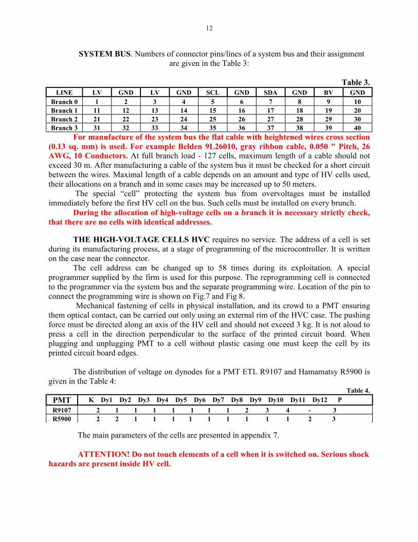
THE HIGH-VOLTAGE CELLS HVC requires no service. The address of a cell is setduring its manufacturing process, at a stage of programming of the microcontroller. It is writtenon the case near the connector.
The cell address can be changed up to 58 times during its exploitation. A specialprogrammer supplied by the firm is used for this purpose. The reprogramming cell is connectedto the programmer via the system bus and the separate programming wire. Location of the pin toconnect the programming wire is shown on Fig.7 and Fig 8.
Mechanical fastening of cells in physical installation, and its crowd to a PMT ensuringthem optical contact, can be carried out only using an external rim of the HVC case. The pushingforce must be directed along an axis of the HV cell and should not exceed 3 kg. It is not aloud topress a cell in the direction perpendicular to the surface of the printed circuit board. Whenplugging and unplugging PMT to a cell without plastic casing one must keep the cell by itsprinted circuit board edges.
The distribution of voltage on dynodes for a PMT ETL R9107 and Hamamatsy R5900 isgiven in the Table 4:
Table 4.PMT K Dy1 Dy2 Dy3 Dy4 Dy5 Dy6 Dy7 Dy8 Dy9 Dy10 Dy11 Dy12 PR9107 2 1 1 1 1 1 1 1 2 3 4 - 3R5900 2 2 1 1 1 1 1 1 1 1 1 2 3
The main parameters of the cells are presented in appendix 7.
ATTENTION! Do not touch elements of a cell when it is switched on. Serious shockhazards are present inside HV cell.
13
14
15
System control.
The control of the high-voltage system is provided by means of commands of theMONITOR via a serial communication line. The MONITOR is the specialized program forinformation exchange between SM512 and controlling computer. This program is stored in aROM of the microcontroller of the system unit. The MONITOR can work with any terminal orcomputer via a serial communication port RS-232 or via CAN bus. It always acceptedsimultaneously commands coming from both RS232 and CAN bus ports but replies only to oneport at the same time – either RS232 or CAN. This depends on value of internal variable stored inthe controller EEPROM (see description of the “Bs” and “Bc” commands).
Settings of the RS232 and CAN bus is stored in the controllers EEPROM (seeAppendix 5 - description of the parameters stored in EEPROM). Controller is shipped withthe following RS232 default port settings:
Baud rate - 9600;Data bits - 8 bits;Stop bits - 1 bit;Parity - None.
Description of the SM-512 microcontroller commands.
All commands of the microcontroller are divided into several main groups according totheir functional assignments.
I. Commands of the status of the system unit.II. Commands controlling the power supply.III. Commands controlling cell.IV. Cells detection commands.V. Commands addressed simultaneously to all cells.VI. Service commands.VII. Test commands.
I. Commands of the status of the system unit.
The "M" command - reads the status of the system module.The format of the command is "M".The format of the reply is 2 bytes. First byte LM is the status of the power controlling
register. Lower 4 bits BV (base voltage), upper 4 bits LV (low voltage) 1 – on, 0 - off. See alsoapp.1 - logic of protection of supply voltages.
Second byte bits (starting from low) correspond to H, T and S.Bit H - represents a status of an external signal blocking high voltage of the system unit
(HV OFF).H=1 HV is enabled, H=0 generation of high voltage is disabled (HV OFF).The signal “ HV OFF” switches off BV simultaneously at all branches of the SM-512
unit. This signal is accepted via the "LEMO" connector (labeled "HV OFF"), which is locatedbelow branches power indicators. When it is in the TTL "0" state generation of high voltages bycells is disabled.
16
T - represent a status of the overheating protection system.T=0 no overheating, T=1 overheating of the system unit. See also app. 2 - logic of the system unitprotection from overheating.
S - S=1 means, that the power lines BV were switched off by the microcontroller after 2minutes after detection of overheating.
The "P" command - reads the 8 values of voltages on power lines.The format of the command is "P".The format of the reply is 8 bytes.
Each byte represents data from corresponding channel of the analog-to-digital converter(0-255).The leading four bytes correspond to the voltages on BV lines 0,1,2,3.Real voltage on a BV line is U(BV)=x*1,067 (volt).The trailing four bytes correspond to the voltages on LV lines 0,1,2,3.Real voltage on a LV line is U(LV)=x*0,024 (volt).
II. Commands controlling the power supply.
The "E" command - switches on (enable) a BV power lines (i.e. 100-200V lines) from whichhigh voltages are generated in cells.The format of the command is "Eb", where b binary number of a branch - 0,1,2,3.The reply is one byte. 0-OK, or error code if error appeared during the execution of thecommand.
Switching on BV power lines on branches is indicated by the red light emitting diode ona front panel of SM512.
The "O" command - switches off BV.The format of the command is "Ob", where b binary number of a branch - 0,1,2,3.The reply is one byte, 0-OK - the generation of high voltages by cells stopped. If error appearedduring the execution of the command the reply contains an error code.
The "_" command - switches off LV power supply (+ 5V).The format of the command is "_b", where b binary number of a branch - 0,1,2,3.The reply is one byte, 0-OK or error code.In normal state and after power on the LV lines are always switched on. They could be switchedoff to reset all the cells on the branch. Before switching off LV controller switches offcorresponding BV. The generation of high voltages by cells stopped. It is not possible to switchon BV when LV is off.
The "#" command - switches on LV power supply (+ 5V).The format of the command is "#b", where b binary number of a branch - 0,1,2,3.The reply is one byte, 0-OK or error code.
III. Commands controlling cell.
The "Z" command – writes one byte into subaddress of a cell with the specified address.The format of the command is "Zsbad", where
17
- s binary subaddress inside cell. For assignment of subaddresses inside the cell see appendix 4.- b binary number of a branch - 0,1,2,3.- a binary address of the cell 1-127- d - data byte to write.The reply is one byte, 0-OK or error code.
The "H" command – reads one byte from subaddress of a cell with the specified address.The format of the command is "Hsba", where- s binary subaddress inside cell. For assignment of subaddresses inside the cell see appendix 4.- b binary number of a branch - 0,1,2,3.- a binary address of the cell 1-127The length of reply can be one or two bytes. First byte is an error code. If error code is 0 i.e. OKthe second byte in the reply contains data. If error code is not equal 0 the reply consist only fromone byte i.e. data byte is not send.
IV. Cell detection commands.
The "l" command - scans cells on all branches and addresses (look for cells).The format of the command is "l".The format of the reply is “l<space>OK<CR><LF>”The command is fulfilled rather long time (about 2.5 sec.).
The results of scanning are stored in memory of the microcontroller of the SM512 unit.This command must be executed before any of the commands addressed simultaneously to allcells. See also section V.
The "R" command - represents in binary format the result of scanning of cells by thecommand "l".The format of the command is "R".The reply consists of 4*127 bytes. Every byte corresponds to one cell. If cell exists thecorresponding byte=1 otherwise it is equal 0. Cells are numbered from 1 to 127 on each branch.
V. Commands addressed simultaneously to all cells.
All commands of this group start with "a". The commands are addressed to all cells,which were found during scanning by the command "l". If the scanning was not performed thecommands of this group will not work!
The "aZ" command – writes one byte into subaddress of all cells.The format of the command is "aZsd", where- s binary subaddress inside cell. For assignment of subaddresses inside the cell see appendix 4.- d - data byte to write.The length of the reply can vary. The first byte is the total number of errors occurred during theexecution of the current command. Then if it is not zero controller sends for every occurred errortwo bytes – the first one is the cell number where error happened and the second byte containsthe error code and the brunch number. The error code occupies lower four bits and the branchnumber – bits 4 and 5.
18
The "aH" command – reads one byte from subaddress of all cells.The format of the command is "aHs", where- s binary subaddress inside cell. For assignment of subaddresses inside the cell see appendix 4.The reply consists of several parts. First part is data block. Its lengths equal to the number ofexisting sells i.e. cells detected by the command “l”. The lengths of the data block is always equalto the number of existing sells even if some cells were read out with errors. The correspondingdata are not valid in this case. The second part of the reply is error report. It is the same as in“aZ” command. The first byte is the total number of errors occurred during the execution of thecurrent command. Then if it is not zero controller sends for every occurred error two bytes – thefirst one is the cell number where error happened and the second byte contains the error code andthe brunch number. The error code occupies lower four bits and the branch number – bits 4 and 5.
VI. Service commands.
Most of the commands of this group are intended for test and debugging purposesand should not be used during normal operations.
The "B" command - changes the speed of the RS232 link.The format of the command is "Br", where r corresponds to the speed values:
"9" - 9600 baud; "2" - 19200 baud; "3" - 38400 baud; "5" - 57600 baud; "1" - 115200 baud;
The value of the RS232 speed is stored in the controllers EEPROM (see Appendix 5 - descriptionof the parameters stored in EEPROM). It will stay after the power cycle of the controller.
The "Bc" command – redirect all output to the CAN bus.The format of the command is "Bc".This command has no reply.The corresponding value is stored in the EEPROM (see Appendix 5)
The "Bs" command – redirect all output to the RS232 serial link.The format of the command is "Bs".This command has no reply.The corresponding value is stored in the EEPROM (see Appendix 5)
The ">" command – writes one location into controllers configuration EEPROM.The format of the command is “>AAA,DDD<CR>” whereAAA – ASCII decimal address of the EEPROM. For the EEPROM layout see appendix 5.DDD – ASCII hexadecimal data to be written to the EEPROM.
This command is suppose to be used for the controller configuration only and executed inthe terminal regime. In the reply controller echoes entered data and reports “Ok<CR><LF>”.
The "<" command – reads one location from controllers configuration EEPROM.The format of the command is “<AAA<CR>” whereAAA – ASCII decimal address of the EEPROM. For the EEPROM layout see appendix 5.
19
This command is suppose to be used for the controller configuration only and executed inthe terminal regime. In the reply controller echoes entered data. Then it writes in hexadecimalformat two bytes of data stored at requested location and reports “Ok<CR><LF>”.
VII. Test commands.
The commands of this group suppose not to be used for communication of thecontrol program with the controller. They are dedicated for manual tests in terminal modeusing any available RS232 communication program like minicom (Linux) orHyperTerminal (Windows).
The "m" command - read the status of the system module.The format of the command is "m".
The format of the reply - s=LM H=0/1 T=0/1 S=0/1 <CR> <LF>, where: s = LM - hexadecimal number representing the status of the power controlling register.
Lower 4 bits BV (middle voltage), upper 4 bits LV (low voltage) 1 – on, 0 - off. See also app.1 -logic of protection of supply voltages.
H - represents a status of an external signal blocking high voltage of the system unit (HVOFF).H=1 HV is enabled, H=0 generation of high voltage is disabled (HV OFF).
T - represent a status of a overheating protection system.T=0 no overheating, T=1 overheating of the system unit. See also app. 2 - logic of the system unitprotection from overheating.
S - S=1 means, that the power lines BV were switched off by the microcontroller after 2minutes after detection of overheating.
The "p" command - reads the status and 8 values of the ADC measuring voltages on powerlines.
The format of the command is "p".The format of the reply - s=LM xxx yyy zzz ccc vvv bbb nnn mmm <CR> <LF>, where:
s = LM (the same as above) - hexadecimal number representing the status of the powercontrolling register. Lower 4 bits BV (middle voltage), upper 4 bits LV (low voltage) 1 – on, 0 -off. See also app.1 - logic of protection of supply voltages.
xxx yyy zzz ccc vvv bbb nnn mmm - data from 8 channels of the analog-to-digitalconverter (0-255).Numbers x, y, z, c - corresponds to the voltages on BV lines 0,1,2,3.
Real voltage on a BV line is U(BV)=x*1,067 (volt).Numbers v; b; n; m - corresponds to the voltages on LV lines 0,1,2,3.
Real voltage on a LV line is U(LV)=x*0,024 (volt).
The "r" command - shows the result of scanning of cells by the command "l".The format of the command is "r".
It represent the address of all cells, which are "seen" by the system.
The "e" command - switches on (enable) a BV power lines i.e. power line 100-200V, fromwhich high voltages are generated in cells.
The format of the command is "eb", where b ASCII number of a branch - 0,1,2,3.
20
The "o" command - switches off BV.The format of the command is "ob", where b ASCII number of a branch - 0,1,2,3. The
generation of high voltages by cells stopped.
The "0" command - switches off (0 volts) LV power supply (+ 5V).The format of the command is "0b", where b ASCII number of a branch - 0,1,2,3.In normal state and after power on the LV lines are always switched on. They could be
switched off to reset all the cells. Before switching off LV controller switches off correspondingBV. The generation of high voltages by cells stopped. It is not possible to switch on BV when LVis off.
The "5" command - switches on LV power supply (+ 5V).The format of the command is "5b", where b ASCII number of a branch - 0,1,2,3.
The "h" command – reads one byte from subaddress of a cell with the specified address.The format of the command is "hss,b,aaa<CR>", where- ss ASCII subaddress inside cell. For assignment of subaddresses inside the cell see appendix 4.- b ASCII number of a branch - 0,1,2,3.- aaa ASCII decimal address of the cell 1-127- the values ss, b and aaa must be separated by commas.The retrieved datum is presented in decimal format.
The "z" command – writes one byte into subaddress of a cell with the specified address.The format of the command is "zss,b,aaa,ddd<CR>", where- ss ASCII subaddress inside cell. For assignment of subaddresses inside the cell see appendix 4.- b ASCII number of a branch - 0,1,2,3.- aaa ASCII decimal address of the cell 1-127- ddd ASCII decimal data to write- the values ss, b, aaa and ddd must be separated by commas.
Controller also recognizes a number of other service and test commands but they shouldbe used only by authorized personal.
Appendix 1 - logic of supply voltages protection.
The microcontroller of the system unit once per every 4 seconds checks the values of LVand BV voltages. If one of these voltages doesn't correspond to expected value themicrocontroller disables voltage on this line and installs corresponding status bit in 0. Thereference data are stored in the EEPROM at the addresses 1 and 2. To switch on power linesagain (after fixing the reason of the problem) one need to execute one of the commandscontrolling the power supply. The LV line must be switched on before the BV. It is not possibleto switch on BV when LV is switched off.
21
Appendix 2 - logic of the system unit overheating protection.
When temperature inside the system unit reaches the threshold value (70 C) internal fan(if present) switches on. If in two minutes after this event temperature doesn't come back tonormal value all power lines are switched off i.e. generation of high voltages stopped. The fan isoptional. It may be installed in SM512 system modules which will be used outside the ventilatedcrates.
Appendix 3 – list of the microcontroller error codes (messages).
Error '1' - No Acknowledge from slave cell.
Error '2' - Arbitration lost on system bus.
Error '3' - Bus is stuck.
Error '4' - Timeout on the bus.
Error '5' - Brunch or LV channel doesn't exist.
Error '6' - Can not Switch On BV because of temperature protection.
Error '7' - Can not Switch On BV because of LV protection.
Error '8' - Unknown command.
Error '9' - Timeout communicating with branch controller (AT89C2051).
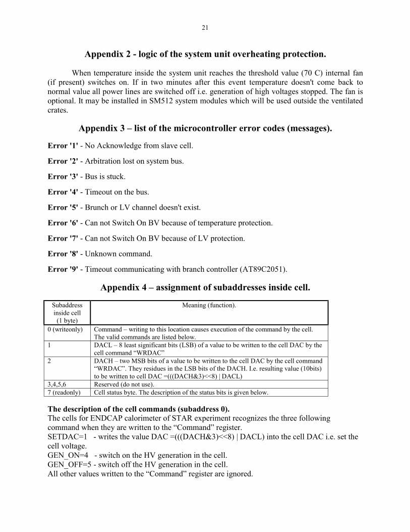
Appendix 4 – assignment of subaddresses inside cell.
Subaddressinside cell(1 byte)
Meaning (function).
0 (writeonly) Command – writing to this location causes execution of the command by the cell.The valid commands are listed below.
1 DACL – 8 least significant bits (LSB) of a value to be written to the cell DAC by thecell command “WRDAC”
2 DACH – two MSB bits of a value to be written to the cell DAC by the cell command“WRDAC”. They residues in the LSB bits of the DACH. I.e. resulting value (10bits)to be written to cell DAC =(((DACH&3)<<8) | DACL)
3,4,5,6 Reserved (do not use).7 (readonly) Cell status byte. The description of the status bits is given below.
The description of the cell commands (subaddress 0).The cells for ENDCAP calorimeter of STAR experiment recognizes the three followingcommand when they are written to the “Command” register.SETDAC=1 - writes the value DAC =(((DACH&3)<<8) | DACL) into the cell DAC i.e. set thecell voltage.GEN_ON=4 - switch on the HV generation in the cell.GEN_OFF=5 - switch off the HV generation in the cell.All other values written to the “Command” register are ignored.
22
Examples:1. To switch on the HV in the cell 15 on branch 1 the command “Zsbad" must be executed,
where Z=90=0x5a i.e. ASCII letter ‘Z’, s=0 – position of the command register in the cell,b=1 – brunch number, a=15 – cell address, d=5 – command GEN_ON.
2. To set the maximal Voltage in the same cell the following commands must be executed –“Zsbad” where s=1 – DACL position inside the cell, b=1, a=15, d=0xff.“Zsbad” where s=2 – DACH position inside the cell, b=1, a=15, d=3 – only two bits are valid.
“Zsbad” where s=0 – Command position inside the cell, b=1, a=15, d=1- commandSETDAC itself.3. To switch off all cells at all branches the following command must be executed – “aZsd” where ‘a’ and ‘Z’ – ASCII letters, s=0 – Command position inside the cell, d=5 –command GEN_OFF itself.
The description of the status bits (subaddress 7).Bit 0 - ER/NOER - the value of this bit shows if the cell working properly on the moment of thereadout.
If the generation of high voltage in the cell is switched on (OFF/ON=1) and this bit hasvalue =0 the cell operates correctly (generates preset voltage). If the generation of the highvoltage is switched off (OFF/ON=0) this should result in ER/NOER=1 for a good cell. In caseof value of the bit ER/NOER=0 while OFF/ON=0 means fault of the self-diagnosis of the cell i.e.the cell is broken.
Bit 1 - OFF/ON - the Generation of high voltage is switched off (0) or switched on (1);
Bit2 - ACCUMER/NOACCUMER - the value of this bit is similar to the ER/NOER, but it is"accumulated" error for a time since the moment of the previous cell status readout, i.e. if for theindicated period the error check circuit inside the cell detected at least one error condition. Thisresults in ACCUMER/NOACCUMER =1. After every readout of cell status byte this bit iscleared.
For a normal situation, when both supply voltages LV and BV are switched on and whenin an interval between two readouts of the status of a cell there were no commands changing itsoperation regime status should be 010 (binary). In general status word could reflect thefollowing situations:
010 - The cell is switched on and works properly.110 - The cell is switched on, currently working properly and there was a fault since the
time past from the previous status readout.111 - The cell is switched on and is not working properly.000 - The cell is switched off and it is faulty.100 - The cell is switched off, at the moment working properly but there was a fault
since the time past from the previous status readout.001 - The cell is switched off and there is a fault on the moment of the status readout;101 - The cell is switched off and works properly.
Only cells with the status 010 or 101 can be considered as working properly. On the otherhand after execution of commands changing the value of high voltage in the cell the output
23
voltage can reach the new set value in rather long time (which can reach several seconds).During transient processes error detection comparator can issue an error, therefore error statusbits can take any values. As a result, correctness of the cell operation can be checked only aftersome time after command changing the working regime of the cell. The HV setup time of cell canvary depending on its type.
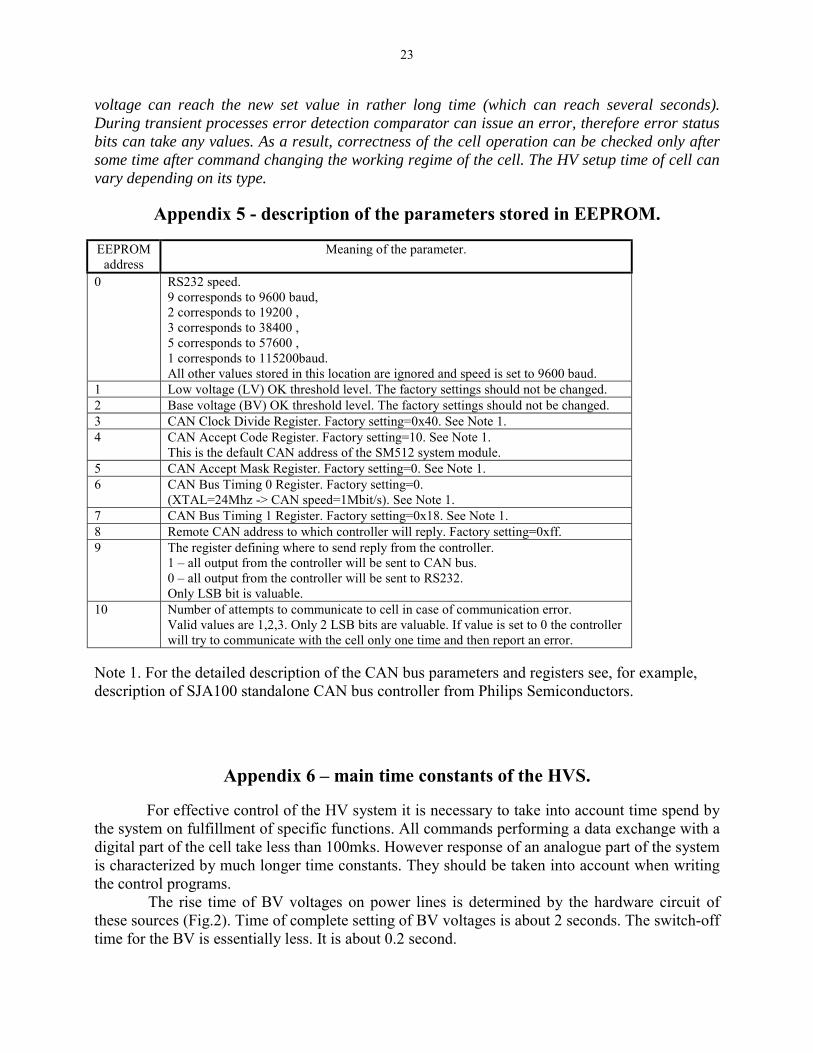
Appendix 5 - description of the parameters stored in EEPROM.
EEPROMaddress
Meaning of the parameter.
0 RS232 speed.9 corresponds to 9600 baud,2 corresponds to 19200 ,3 corresponds to 38400 ,5 corresponds to 57600 ,1 corresponds to 115200baud.All other values stored in this location are ignored and speed is set to 9600 baud.
1 Low voltage (LV) OK threshold level. The factory settings should not be changed.2 Base voltage (BV) OK threshold level. The factory settings should not be changed.3 CAN Clock Divide Register. Factory setting=0x40. See Note 1.4 CAN Accept Code Register. Factory setting=10. See Note 1.
This is the default CAN address of the SM512 system module.5 CAN Accept Mask Register. Factory setting=0. See Note 1.6 CAN Bus Timing 0 Register. Factory setting=0.
(XTAL=24Mhz -> CAN speed=1Mbit/s). See Note 1.7 CAN Bus Timing 1 Register. Factory setting=0x18. See Note 1.8 Remote CAN address to which controller will reply. Factory setting=0xff.9 The register defining where to send reply from the controller.
1 – all output from the controller will be sent to CAN bus.0 – all output from the controller will be sent to RS232.Only LSB bit is valuable.
10 Number of attempts to communicate to cell in case of communication error.Valid values are 1,2,3. Only 2 LSB bits are valuable. If value is set to 0 the controllerwill try to communicate with the cell only one time and then report an error.
Note 1. For the detailed description of the CAN bus parameters and registers see, for example,description of SJA100 standalone CAN bus controller from Philips Semiconductors.
Appendix 6 – main time constants of the HVS.
For effective control of the HV system it is necessary to take into account time spend bythe system on fulfillment of specific functions. All commands performing a data exchange with adigital part of the cell take less than 100mks. However response of an analogue part of the systemis characterized by much longer time constants. They should be taken into account when writingthe control programs.
The rise time of BV voltages on power lines is determined by the hardware circuit ofthese sources (Fig.2). Time of complete setting of BV voltages is about 2 seconds. The switch-offtime for the BV is essentially less. It is about 0.2 second.
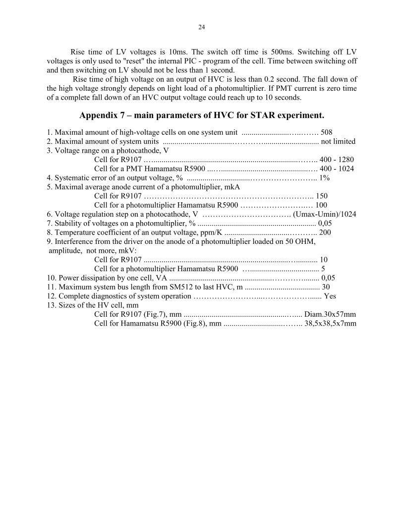
24
Rise time of LV voltages is 10ms. The switch off time is 500ms. Switching off LVvoltages is only used to "reset" the internal PIC - program of the cell. Time between switching offand then switching on LV should not be less than 1 second.
Rise time of high voltage on an output of HVC is less than 0.2 second. The fall down ofthe high voltage strongly depends on light load of a photomultiplier. If PMT current is zero timeof a complete fall down of an HVC output voltage could reach up to 10 seconds.
Appendix 7 – main parameters of HVC for STAR experiment.
1. Maximal amount of high-voltage cells on one system unit ........................…..……. 5082. Maximal amount of system units ...................................…………............................ not limited3. Voltage range on a photocathode, V
Cell for R9107 .….........................................................................…….. 400 - 1280Cell for a PMT Hamamatsu R5900 ...…............................................…. 400 - 1024
4. Systematic error of an output voltage, % ................................…………………….. 1%5. Maximal average anode current of a photomultiplier, mkA
Cell for R9107 ……………………………………………………….. 150Cell for a photomultiplier Hamamatsu R5900 …………………….… 100
6. Voltage regulation step on a photocathode, V ……………………………. (Umax-Umin)/10247. Stability of voltages on a photomultiplier, % ............................................................ 0,058. Temperature coefficient of an output voltage, ppm/K .................................……….. 2009. Interference from the driver on the anode of a photomultiplier loaded on 50 OHM, amplitude, not more, mkV:
Cell for R9107 .........................................................................…........... 10Cell for a photomultiplier Hamamatsu R5900 …................................... 5
10. Power dissipation by one cell, VA ....................................................…………........ 0,0511. Maximum system bus length from SM512 to last HVC, m ...................................... 3012. Complete diagnostics of system operation ……………………...………………...... Yes13. Sizes of the HV cell, mm
Cell for R9107 (Fig.7), mm ....................................................….... Diam.30x57mmCell for Hamamatsu R5900 (Fig.8), mm ..............................…….. 38,5x38,5x7mm