Embed Size (px)
Citation preview

THE SINGER COMPANYKEARFOTT DIVISIONY256A226 REV.-
CONTRACT NO. NAS 9-13144DRD NO. MA-129TA
(NASA-CR-134188) SOLID STATE SWITCHPANEL Final Report (Singer Co., Little N74-16954Falls, N.J.) 115 p HC $8.75 CSCL 09E
SUnclas
G3/09 30454
FINAL REPORT
FOR
SOLID STATE SWITCH PANEL
26 NOVEMBER 1973
Prepared by: Approved by:
7. eenfe t J. AttwoollProject Engineer Engineering Manager
F4202-1 2/72
https://ntrs.nasa.gov/search.jsp?R=19740008841 2020-05-14T12:07:52+00:00Z

THE SINGER COMPANY Y256A226KEARFOTT DIVISION REV.
DISTRIBUTION LIST
NASA Manned Spacecraft Center 1 copy
R&T Procurement BranchAttn: Ted Lapko, Mail Code BC731(38)Houston, Tx. 77058
NASA Manned Spacecraft Center 4 copies
Technical Library BranchAttn: Retha Shirkey, Mail Code JM6
Houston, Tx. 77058
NASA Manned Spacecraft Center 1 copy
Management Service DivisionAttn: John T. Wheeler, Mail Code JM7
Houston, Tx. 77058
NASA Manned Spacecraft Center 4 copies
Power Distribution and Control Branch 1 reproducible
Attn: A.B. Olsen, Main Code EB3Houston, Tx. 77058
ii
F4202-1 2/72

THE SINGER COMPANYKEARFOTT DIVISION Y256A226 REV.
ABSTRACT
An intensive study of various forms of transducers was conducted
with application towards hermetically sealing the transducer pick
off and all electronics. The results of the study indicated that
the Hall effect devices and a LED/phototransistor combination
were the most practical for this type of application. Therefore,
hardware was developed utilizing a magnet/Hall effect transducer
for single action switches and LED/phototransistor transducers
for rotary multiposition or potentiometer applications. All
electronics could be housed in a hermetically sealed compartment.
A number of switches were built and models were hermetically
sealed to prove the feasibility of this type of fabrication. One
of each type of switch was subjected to temperature cycling, vib-
ration, and EMI tests. The results' of these tests are indicated
in the following report.
PRECED N&M 140T UMM
iii
F4202.1 2/72

THE SINGER COMPANYKEARFOTT DIVISION Y256A226
TABLE OF CONTENTSPage
Introduction 1-1Technical Description 2-1Transducers 2-1Circuitry 2-23Switch Configuration 2-24Power Consumption 2-32Panel Operation 2-33Tests 3-1Functional 3-1Environmental 3-1Reliability 4-1Appendix I-1
iv
F4202-1 2/72

THE SINGER COMPANYKEARFOTT DIVISION Y256A226 REV.
RESULTS
The results of this project are:
1. An operating switch panel conforming to the requirementsof NAS-9-13144.
2. Test data taken during environmental tests performed onselected switch and rotary components. The tests per-formed were comparable to tests run on NASA flighthardware delivered on the skylab project. Satisfactoryresults were obtained on all tests.
3. Reliability data indicating MTBF for selected devices.
4. A project report covering the study phase of the projectand containing test data, schematics, and outlinedrawings of the switch devices and the mounting panel.
v
F4202-1 2/72

THE SINGER COMPANYKEARFOTT DIVISION Y256A226 REV.
CONCLUSIONS
The results of this project indicate that solid state switches
and rotary components capable of meeting the requirements of
manned space flight are feasable and well within the current
state of the art. The environmental and reliability data indicate
that a production unit would have the superior reliabilityassociated with solid state equipment. The large selection of
contact closure types will allow switches to be fitted to various
requirements. A phase II production type unit would be packagedin a smaller and lighter housing. The feel of each switch and
the front panel appearance would be improved in the phase II
design.
viF4202-1 2/72

THE SINGER COMPANYKEARFOTT DIVISION Y256A226 REV.,
RECOMMENDATION
The study indicated that the most efficient switch is one designedto switch a specified voltage and current. Using a high current
switch to handle a low current is inefficient. Any production
switches should be designed for a specific power level.
In production quantities a hybrid package containing all the
electronics is recommended as a way to save size and increasereliability of the solid state switch devices.
Reduction of switch size would allow the toggle section of the
switch to be brought flush to the panel surface and otherwise
improve the appearance of the switches.
It is also recommended that a closer analysis of the front panelremovability criteria be made with an effort to reduce thepanel area used for fastening.
viiF4202.1 2/72

THE SINGER COMPANYKEARFOTT DIVISION Y256A226 REV.
INTRODUCTION
The purpose of this report is to summarize the results of astudy conducted to determine the optimum transducer type and out-put circuitry for a solid state switch configuration and todemonstrate with hardware, the feasibility of the resulting de-signs. Two basic types of switches are required, a single actionswitch (toggle, pushbutton) and a multiposition rotary switch and/or potentiometer. The switches will be designed to be hermet-ically sealed and removable as an integral unit from the frontof the panel. Selected switches contain a Light Emitting Diode(LED) display indicating the status of the switch position and/oroperable or failure mode.
The various types of transducers studied included the following:
" Light
* Capacitive
* Hall effect
* Magneto-resistor
Many factors were considered in selecting the appropriate trans-ducer for the application and the necessary circuitry for theswitch output. They were as follows:
* Type of excitation required
* Power required
* Cost
* Size
* Reliability
* Hermetic sealing capability
* Cross talk effects
* Packaging
e Switching characteristics
A matrix indicating these characteristics of the various transducersare shown in Table I.
1-1F4202 1 2/72

C
TABLE I. TRANSDUCER MATRIX
HALL MAGNETOLIGHT CAPACITANCE EFFECT RESISTOR
POWER .150 WATTS .100 WATT .050 WATT .050 WATT
EXCITATION DC 5-10V AC 10 KHZ DC 5-10V DC 5-10W
COST MODERATE HIGH LOW MODERATE
CROSS TALK NONE PROBLEM AREA NONE NONE
HERMETIC SEAL PROBLEM AREA PROBLEM AREA COMPATABLE COMPATABLEGLASS TO MET- GLASS TO MET-AL SEAL AL SEAL mm
.z
SIZE MODERATE LARGE SMALL MODERATE O 0
COMPONENTS TWO SILICON TWO SEALED ONE INTEGRA- ONE SEMI- z oSEMI-CONDUC- METAL PLATES TED CIRCUIT CONDUCTOR oTORS AND AND DRIVE AND MAGNET AND DRIVEGLASS SEAL CIRCUITRY CIRCUITRY z z
SWITCHING REQUIRES REQUIRES TRIGGER TRIGGERCHARACTERISTICS TRIGGER TRIGGER PART OF IC REQUIRED
N,
I,

THESINGERCOMPANY Y256A226KEARFOTT DIVISION REV.
The results of the study indicated that the Hall effect trans-ducer is the most effective for the single action switch and theLED/phototransistor is the optimum device for the multipositionrotary switch and potentiometer.
Dependent upon the function of the switch, four types of outputcircuits were selected to interface with peripheral equipment.The determining factor in the circuitry was the contact rating ofthe switch.
* High current DC (10 AMP)
* Medium current DC (400 MA)
* Low current Analog (50 MA)
* Low current AC (I AMP)
To insure reliable operation, redundant circuitry has been inclu-ded wherever size and circuitry dictates practicability. Thesubject of man-hardware interface has not been discussed becausestandard mechanical switch actuating devices are used for inputswith normal actuating pressure loads and travel.
Envelope drawings and schematics are included in the appendices(Section 8) indicating the design approach configurations for thePhase I program. Production versions of these modules would re-quire some modification for facility of fabrication and appearance.As a result of the study program, a panel was fabricated including25 single pole or double pole toggle and pushbutton switches, tworotary 10 position switches and two potentiometers as indicatedin Figure 1.
1-3
F4202-1 2/72

POWER SWITCHES POTENT IOMETERS0
No. I No. 2 No. I No. 2
e 0 0 e
MOMENTARY SWITCHES4-00 M A
[ SINGLE POLE I t DOUBLE POLE
MAINTAINED SWITCHES
SINGLE POLE I100 MA DOUBLE POLE I
LII2 IZ 1 i LIs LI ? LI
PUSHBUTTON SWITCHES
r-DOUBLE POLE 24 0 V. RMS -1 - 5INGLE POLE'i20V.RMS.
LI. 4. O LZI
ROTARY SWITCHES
No.I No. 2
PUSHBUTTONMOMENTARY SWITCHES SWITCHES
oOU8LE PotF2q0V RMS
ISL Ia) SI tr
MAINTAINED SWITCHESPOWER PANEL SINGLE POLE
2- ON aov
5SV SA otd . 'a.s, OFF sMA. Sal s s
POTENTIOMETER ROTARY SWITCHES2 r2-
. 4 _0. 0 D D
5/ -- i --- 2 VAc
Lo 0o uo 1
FIGURE 1 SOLID STATE SWITCH PANEL
1-4

THE SINGER COMPANY Y256A226KEARFOTT DIVISION REV.
TECHNICAL DESCRIPTION
The following four basic areas were studied in order to producethe required switch/potentiometer configurations for the switchpanel:
* Transducers
* Mechanical Packaging
• Output (switch contact) circuitry
• Solid state potentiometer circuit configurations
TRANSDUCERS
Many types of transducers were evaluated to determine the optimumswitch transfer. For each transducer the source and sensor of theswitching medium is discussed along with the various configurations.
MAGNETIC CIRCUIT TRANSDUCER
A magnetic circuit transducer depends on changing magnetic fluxfor switching action. A mechanical switch change occurring ex-ternal to the hermetic seal changes the reluctance of the mag-netic circuit. This flux change is sensed inside the hermeticseal and interfaced with the logic section of the switch. Bothalternating and direct flux devices have been reviewed.
DC Devices
The flux flows in only one direction in a direct flux circuit andis a function of the following relationship.
MMFR
A change in the flux is sensed and a typical simple switch isillustrated in Figure 2. With the switch open as in Figure 2 ahigh reluctance air gap exists in the magnetic circuit. If themissing slug is moved into the gap, the reluctance is diminished.This increases the flux and changes the characteristics of theflux sensing element. Two sources of mmf appear most appropriatefor switch applications: permanent magnets or solenoid coils.Permanent magnets require the following characteristics to beeffective.
2-1F42
02 12/72

THE SINGER COMPANYKEARFOTT DIVISION Y256A226 REV.
MECHANICAL - LOW RELUCTANCEACTUATION MAGNETIC CIRCUIT
FLUX HERMETIC
SOURCESEAL
FLUX SENSOR
FIGURE 2
2-2
F4202-1 2/72

THE SINGER COMPANYKEARFOTT DIVISION Y256A226 REV..
* Small size
" High induction
* High demagnetization force
Of the present commercially available magnetic materials, thefollowing best suit these characteristics:
* Ceramic permanent magnets
* ALNICO SERIES*
* Gecor*
The life characteristic of these materials (t-ne of retention ofuseful magnetic properties) has been estimated at approximately15 years.
Solenoid coils require electrical power in order to operate.However, these devices utilize materials which are more readilyavailable than magnets and do not require any special handlingtechniques as is sometimes the case with magnets. Of the fluxsensing elements available the following exhibit the most suitableproperties for switch application:
* Pick up coil
* Hall effect device
* Magnetic resistor
" Pick Up Coil - The simplest of the three devices is a pickup coil which is a coil of wire of many turns wound aroundthe magnetic core. This coil does not require a gap in themagnetic circuit which greatly increases the reluctanceand, therefore, reduces the magnetic strength required.Many magnetic materials can be used for this application.The greatest disadvantage of using a pick up coil in adirect flux circuit is the fact that a coil can only sensea change in flux. Therefore, an output voltage would onlybe available from the coil during switching transition.After the coil has reached a different steady state valveas a result of the new switch position no voltage is pres-ent at the coil. The logic necessary to sense these
*Trade name of a General Electric Co. product
2-3F4202-1 2/72

THE SINGERCOMPANYKEARFOTT DIVISION Y256A226 REV._.
transient pulses is relatively simple, however, the prob-lem exists in the initial start up procedure. The use of
this device is limited to momentary switch applicationswhere the switch mode of operation is in the normally offcondition.
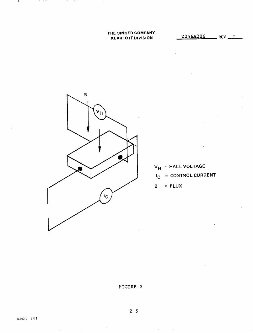
* Hall Effect Device - The Hall effect element is a semicon-ductor device that generates a voltage as a function ofcontrol current and magnetic field. As illustrated in
Figure 3 control current is passed through one axis of thesemiconductor. The Hall voltage will appear perpendicularto the control current at the edges of the semiconductor
chip. This voltage will be a function of the magneticflux passing through the chip perpendicular to both controlcurrent and the output voltage. In the switch application,this voltage is used to control the switch output. Theadvantages of the Hall effect device are:
* Small size
* Detection of steady state flux levels
" Life and reliability similar to silicon semiconductors
Because the Hall effect device has a relatively low outputvoltage (in the order of 50mv) an amplification stage isnecessary as an interface between the transducer and theswitch output circuitry. The control current requiredfor the Hall effect device is approximately 5 - 50 MA.The Hall effect device is made very thin (.006 inchestypical) in order to retain a high flux density acrossthe Hall device in the on condition.
A device available from Honeywell Microswitch incorporatesa Hall effect device and an amplifier and trigger circuitin one integrated chip. This device operates on low levelsof flux and provides as an output two current sinks. Inaddition to being small and sensitive this magneticswitch requires very little power to operate (30 mw max.at 5 volts). This power level is equivalent or lower thanmost flux sensing devices made of discrete parts.
The device has been designed to operate over the stan-dard Military temperature range (-550C -- +125 0 C) andis available off the shelf from Micro-Switch. The deviceis sensitive enough that no specific flux path need beincorporated in the hermetic seal. The switch will sense
2-4
F4202-1 2/72
THE SINGER COMPANYKEARFOTT DIVISION Y256A226 REV.
VH
VH = HALL VOLTAGE
IC = CONTROL CURRENT
B = FLUX
IC
FIGURE 3
2-5
F4202
-1 2/72

THE SINGER COMPANY Y256A226KEARFOTT DIVISION REV.
the presence of a small magnet at distance of .090 in. with anynon-magnetic material between the magnet and the sensor. Thisfeature will greatly simplify the process of hermetically sealingthe final package.
* Magneto Resistor - Magneto resistors are solid statepassive devices that change their resistance in the pre-sence of a magnetic field. The devices are thin crystalsof Indium Antimonide with electrical connections at bothends (Reference Figure 4a). The crystal is a semicon-ductor with a grid-like conducting material running per-pendicular to the direction of the current flow. Withno flux passing through the device current flows perpen-dicular to the conducting bands implanted in the semi-conductor. Under these conditions the device exhibitsits lowest resistance. If flux is allowed to pass throughthe device, the current is forced to travel a greaterdistance between conducting bands (Reference Figure 4b).The longer current path increases the resistance betweenthe ends of the device. Typical ratios between maximumand minimum resistance are on the order of 13 to 18 forsensitive devices. The application of the magnetoresistor is similar to the Hall effect devices in thatthey are mounted in the gap in the magnetic circuit.Magneto resistors have the following advantages:
* Small size
* Low power
* Life and reliability similar to silicon semiconductors
Power consumption of magneto resistors is a function of the inputcurrent and resistance and is, therefore, in the order of mw.
Alternating Magnetic Flux Devices
Alternating magnetic flux can also be used to convey mechanicalswitch status through a hermetic seal. Switches of this typeoperate using transformer coupling. This method would requirethe use of AC signals inside the hermetic seal. Because AC
signals must be generated to produce the alternating flux andlater rectified to interface with the logic and switch sections,this method will consume more power and be more complex thandirect flux circuits.
2-6F
4 2 0 2 -1 2/72

THE SINGER COMPANY Y256A226
KEARFOTT DIVISION REV.
B
B=O BAO
FIGURE 4
2-7
f4202-1 2/72

THE SINGER COMPANYKEARFOTT DIVISION Y256A226 REV.
The only source of alternating flux convenient for use in thisapplication is a coil of wire around the magnetic flux path.The optimum frequency at which the flux should oscillate will bea function of core losses in the magnetic circuit, the size ofthe oscillator, and the amount of radiated energy acceptable.
The greatest disadvantage to this type of design is the possibleenergy radiated to other switches and circuitry behind theswitch. This radiation can be minimized to some extent by plac-ing a magnetic shielding around the switch and EMI filters onthe electrical lines, however, this would complicate both thepackaging and the manufacture of the final switch.
All the sensors which sense direct flux also sense alternatingflux. Of the three types discussed (pick up coil, Hall effect,magneto resistor), the pick up coil is the most adaptable toalternating flux. A transformer type switch using coils mightoperate as follows:
SN2 N1
In the configuration above, coil N1 is not strongly coupled withcoil N2. Coil N2 is a feedback circuit for the oscillator.With the slug removed from the magnetic path the feedback is in-sufficient to maintain oscillation. This results is a zero volt-age output at the full wave rectifier. If the missing part ofthe core is placed into the magnetic circuit, coil N1 is coupledto coil N2 providing feedback to the circuit. This causes thecircuit to break into oscillations and provides a DC voltage atthe full wave rectifier switching the latching logic.
2-8
F4202-1 2/72

THE SINGERCOMPANYKEARFOTT DIVISION Y256A226 REV.
The selection of the material to form the magnetic core, is basedon a number of factors.
* Magnetic properties
" Ease of machining
* Compatibility with switch housing material
* Ability to form hermetic seal.
A material of high relative permeability and low magnetic reten-
tivity is most desirable. This would insure the greatest changein flux for a given magnet. Two materials appear best suited to
this requirement.
1. Cold rolled armco Magnetic input iron.
2. Cold rolled electro-magnetic iron.
When properly heat treated these materials are easily machinedand can be soldered or brazed in the normal fashion.
One other consideration must be made if alternating flux is to
be used. Core losses must be kept to a minimum which will requireeither a laminated core or a ferrite core. Both of these cores
would be difficult to hermetically seal and will complicate themachining and manufacture of the transducer unit.
Transducer Evaluation
In the following section each of the sensors and sources areevaluated, thereby, allowing the best possible combination to bedetermined. A summary at the end of this section compares allthe combinations.
Coil Source With Coil Sensor
This approach is not acceptable because of the inability of thecoil sensor to detect a steady state flux. A memory device ofsome type would be required to hold the switch in either the onor off state after a change in the flux level. Such a transducerwould be further complicated by the circuitry required to guaran-
tee proper start up. When power is first applied to the switch,circuitry must be provided to set the memory in either the on or
off position depending on the position of the moveable coresection.
2-9
F4202-1 2/72

THE SINGER COMPANY Y256A226KEARFOTT DIVISION Y256A226 REV.
Another disadvantage of this method is the coil source whichdissipates electrical power to provide a steady state flux.Permanent magnets use no power to accomplish the same thing.
Coil Source With Hall Effect Sensor
A transducer of this type is feasible. It has two major dis-
advantages which make it less acceptable than other methods to
be described.
1. Power must be supplied to both the coil and the Halleffect device for proper operation. This current wouldbe on the order of 30 ma which is much higher than othertypes of transducers.
2. The Hall effect device puts out a low voltage (40 - 400
my) when magnetic flux passes through it. This voltagelevel would have to be amplified in order to drive logic.The addition of an amplifier would consume more powerand space in the final design and is therefore not de-sirable.
Coil Source With Magneto Resistor Sensor
A transducer of this type offers many advantages. The magnetoresistor requires no control current as does the Hall effectdevice so the total power consumption will be smaller than the
Hall effect. With a flux change of 10 kilogauss the magnetoresister changes its resistance by a factor of 7 from its 0
kilogauss level. This change is enough to actuate logic without
amplification. At worst a single transistor will interface be-tween the transducer and the logic section.
The only drawback to this combination is the coil source whichwill draw current to generate the flux.
Permanent Magnet With Coil Pick Up
This method is unacceptable for reasons mentioned under coilsource coil pick up.
Permanent Magnet With Hall Effect Device
This arrangement has the same drawbacks as the one using Halleffect with coil source. The only advantage is the fact that nocurrent would be required to generate the flux.
2-10
F42 0 2
-1
2/72

THE SINGER COMPANYKEARFOTT DIVISION Y256A226 REV.
The complete transducer circuit is indicated as follows:
VCC VCC
OUTPUT
Permanent Magnet With Magneto Resistor
This combination is acceptable because the flux is generated
without the use of power and the Magneto resistor requires few
additional components and uses little power.
The complete transducer is as follows:
VCC VCC
OUTPUT
MR
2-11
F4202-1 2/72
THE SINGER COMPANYKEARFOTT DIVISION Y256A226 REV.
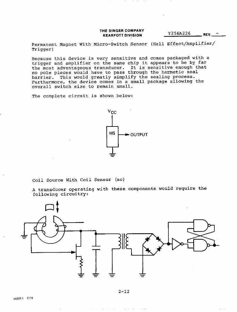
Permanent Magnet With Micro-Switch Sensor (Hall Effect/Amplifier/Trigger)
Because this device is very sensitive and comes packaged with atrigger and amplifier on the same chip it appears to be by farthe most advantageous transducer. It is sensitive enough thatno pole pieces would have to pass through the hermetic sealbarrier. This would greatly simplify the sealing process.Furthermore, the device comes in a small package allowing theoverall switch size. to remain small.
The complete circuit is shown below:
VCC
MS OUTPUT
Coil Source With Coil Sensor (ac)
A transducer operating with these components would require thefollowing circuitry:
2-12
F4202-1 2/72

THE SINGER COMPANYKEARFOTT DIVISION Y256A226 REV..
The variable inductive coupling between the output and the inputcontrols the feedback to the oscillator. Thus, by changing thefeedback, the oscillator can be driven out of oscillation. Byrectifying the output and using this signal to control the logicsection, switch operation can be made.
The following problems complicate this approach to the transducerproblem.
1. The oscillation inherent in this type of switch will bedifficult to shield from the outside world. Use oflarge RF filters would be difficult due to the smallpackage size required.
2. The difficulty in hermetically sealing a low loss ACtype core (laminated or ferrite) would necessitate useof a DC type core. This would force the oscillator towork at a higher power level to offset core losses.
3. Part count for this type of transducer would be highmaking a small package size difficult.
Coil Source With Hall Effect Sensor (ac)
This type of transducer would have all the drawbacks mentionedunder coil source and coil sensor plus the following:
The Hall effect device must be placed in the path of magneticflux requiring a gap in the core of the oscillator decreasingthe coupling. The output from a Hall effect device would be avery small voltage (40 - 10 my).
The Hall effect device requires a control current for operationwhich is an added power requirement not necessary with a coilpick up. This type of transducer is not acceptable because ofthe poor AC flux characteristics of the Hall effect device. Acoil pickup is far superior in every respect for this application.
Coil Source With Magneto Resistor Pick Up
This transducer is unacceptable for the same reasons mentionedunder coil source Hall effect device pick up.
Conclusions
Of all the magnetic transducers discussed in this section, themost acceptable is the Honeywell magnetic switch used in combina-tion with a permanent magnet. It is the best selection for thefollowing reasons.
2-13
F4202 1 2/72

THE SINGER COMPANYKEARFOTT DIVISION Y256A226 REV.
* Low power
" Smallest size of any magnetic transducer
" Lowest component count.
LIGHT TRANSDUCERS
Transducers of this type will direct a beam of light from a lightsource through a shutter arrangement to a light sensor. Bothlight sensor and source will be contained inside a hermetic seal.The shutter arrangement will be external to the hermetic seal.By either allowing the light beam to strike the sensor or inter-rupting the light beam with the shutter, switch control of thelight sensor can be obtained.
SHUTTER----
----- HERMETICI I SEAL
I II
LIGHT LIGHTSENSOR SOURCE
The shutter type of transducer would require that the hermeticseal wrap around the movable shutter. This means a transparenthermetic seal would have to be made at each side of the shutter.To avoid this complicated seal, an alternate configuration witha reflective surface can be used. In this method light isdirected through a transparent hermetic seal towards a reflectivesurface. Upon striking the surface the light beam is directedback toward the light sensor through the same transparent sealthrough which it originally passed. In this way only one
2-14
F42 0 2
-1 2/72

THE SINGER COMPANYKEARFOTT DIVISION Y256A226 REV.
transparent seal is required and both source and sensor can be
placed in the same place. Switching is obtained by either re-
flecting or not reflecting the light beam back to the sensor.
No moving parts are required within the hermetic seal.
LIGHT r[ ROTATING ENCODER DISC.
SOURCE
MIRROREDSHUTTER
LIGHTSENSOR
Light Sources
A beam of light can be obtained from the following sources:
* Incandescent lamp
0 Light emitting diode
• Electro luminescent lamp
The following characteristics would be desirable in a light source:
* Small size
0 High brightness
* Low power
0 Long life
2-15
F4202-1 2/72

THE SINGER COMPANYKEARFOTT DIVISION Y256A226 REV.Z
It would also be desirable to have the light eminate from asingle point source. As the light must be gathered into a beamto pass to the detector a single point source would simplify thisrequirement.
* Incandescent lamps - A light source of this type satisfiesthe size and brightness requirements with no difficulty.Light intensities as high as 2,400 foot LAMBERTS can beobtained in package sizes as small as Figure 5. Thedrawbacks of this source are its power consumption andits limited life. There would be no way to convenientlyreplace the lamp because of the hermetic seal. Thisfactor alone makes use of incandescent lamps PROHIBITIVE.
* Light emitting diode - Light emitting diodes satisfymost of the requirements. They are small, have a verylong life time, moderate power consumption with moderatebrightness. A further advantage of the LED source isits narrow frequency band of light output.
Many types of photo diodes and photo transistors are optimizedfor use at a single frequency. This means that the proper com-bination of LED and photo diode will make more efficient use ofthe light than a combination of photo transistor and any other lightsource.
LED's come in a variety of package sizes. The device picturedin Figure 6 would be most suited to the requirements of thisapplication. This device was designed to be used with a particu-lar photo transistor in high speed card and tape readers. Thecharacteristics of this device are listed in Table II.
* Electro-Luminescent Lamps - This type of lamp would notbe suitable for this application. Electro-luminescentlamps have very low brightness (20 fL) and are bettersuited to surface illumination.
Light Sensors
Light emitting diodes are the best choice for light sources soonly sensors which interface with LED's will be considered. Thefollowing devices are specifically designed to interface with LED's.
* Photo - Diodes
* Photo - transistors
2-16
F4202
-1
2/72

THE SINGER COMPANYKEARFOTT DIVISION Y256A226 REV.
S -. 25 -- .093-2
FIGURE 5
2-17
F4202-1 2/72

THE SINGER COMPANYKEARFOTT DIVISION Y256A226 REV.
.105
.062
FIGURE 6
2-18
F4202-1
2/72

THE SINGER COMPANYKEARFOTT DIVISION Y256A226 REV.
TABLE II. LIGHT EMITTING CHARACTERISTICS
ELECTRICAL CHARACTERISTICS (TA = 250 C unless otherwise noted)
Characteristic Fig. No. Symbol Min Typ Max Unit
Reverse Leakage Current - IR - 50 - nA
(VR = 3.0 V,RL = 1.0
Megohm)
Reverse Breakdown BVR 3.0 - Volts
Voltage
(I R = 100 PA)
Forward Voltage 2 VF - 1. 2 1.5 Volts
(IF = 50 mA)
Total Capacitance CT - 150 - pF
(VR = 0 V, f =1.0 MHz)
OPTICAL CHARACTERISTICS (TA = 250C unless otherwise noted)
Characteristic Fig. No. Symbol Min Typ Max Unit
Total Power Output 3,4 P 50 150 - 1W(Note 1)
(I F = 50 mA)
Radiant Intensity I - 0.66 - mW/
(Note 2) stera-
(I F = 50 mA) dian0
Peak Emission 1 XP - 9000 A
Wavelength
Spectral Line Half 1 AX - 400 - A
Width
The characteristics desirable for this application are:
* Small size
* Compatible with LED light sources
* High light sensitivity
e Low power consumption
2-19
F42 0 2 -1 2/72

THE SINGER COMPANY Y256A226KEARFOTT DIVISION REV.
* Photo Diodes - Photo diodes are P on N or N on P siliconfunction devices that generate a photo current inresponse to a beam of light focused on the sensitivejunction.
Being composed of silicon, these devices are small, rugged andreliable. The photo-diode is the basic photo sensitive devicein all of the photo transistor varieties, so in one form oranother it will be used in any kind of light transducer. Thecurrent voltage curves for a typical photo diode are shown below.
2NDQUADRANT 1ST QUADRANT
(FORWARD BIAS
' -0.6 -0.4 -0.2 0 OPERATION)
\ARK VOLTAGE (VOLTS) - 0.2 0.4 0.6
250 FOOT CANDLES
-20 /50 FOOTCANDLES
3RD QUADRANT /(REVERSE BIAS OPERATION) -40.- / 4TH QUADRANT
1,000 FOOT CANDLES (UNBIASED OPERATION)1,000 FOOT CANDLES
The voltage and current levels are sufficient to drive the logicsection without further amplification. However, if a phototransistor were used, lower light intensities would be able todrive the same logic section. This would mean lower power con-sumption in the LED.
* Photo-transistors - The photo-transistor uses a photodiode to generate base current for a normal transistor.This, in effect, amplifies the current sensitivity ofthe device by the 3 of the transistor. There is nodifference in package sizes between the photo diode andphoto transistor,. both can be obtained in packages assmall as Figure 6.
Photo FETS take advantage of the photo voltaic effect of photodiodes. This is the change in output voltage as a function oflight intensity of an open circuited photo diode. The increaseof current gain available using a photo FET is of the same orderof magnitude as that of a photo-transistor.
2-20'
F42021 2/72

THE SINGER COMPANYKEARFOTT DIVISION Y256A226 REV.
Configurations - The simplest configuration of a light transducer
would look as follows:
RL
OUTPUT
LED PHOTO-TRANSISTOR
LIGHT
In this configuration the light from the LED provides basecurrent for the photo transistor turning it on. The shutter can
be placed in the path of the light beam turning off the transistor.
The LED must be provided with from 20 to 50 ma of current depend-
ing on the distance between the diode and the transistor, theload RL on the transistor, and any attenuating devices betweenthe diode and the transistor (glass, light pipes, etc.).
The configuration of the reflective type transducer would beidentical to that pictured above except for the shutter whichwould become a mirrored surface.
Conclusions
Of the light type transducers the light emitting diode in con-
junction with the photo-transducer is the only method which will
adequately meet the requirements of this application.
2-21
F42021 2/72

THE SINGER COMPANY Y256A226KEARFOTT DIVISION REV.
Table III below lists the characteristics of this type oftransducer.
TABLE III. LIGHT TRANSDUCER CHARACTERISTICS
POWER .150 WATTS
COMPONENT 3COUNT
CROSS NONETALK
EXCITATION DC-5-10V
HERMETIC PROBLEM AREASEAL GLASS TO METAL
SEAL
2-22
F4 2 0 2 -
1 2/72

THE SINGER COMPANYKEARFOTT DIVISION Y256A226 REV.
CAPACITANCE TRANSDUCERS
A transducer of this type would operate by sensing the change ofa capacitor and operating a trigger circuit from this change.Because all electrical components must be contained inside ahermetic seal the only portion of a capacitor which could be usedto change the capacitance would be the dielectric. The plates ofthe capacitor being current carrying devices must lie within thehermetic seal and are therefore inaccessable for mechanicalchange.
This factor makes it very difficult to implement this type oftransducer. Both plates must be sealed behind at least .050thick sheets of glass while the dielectric contained within theenvironmentally sealed section is moved in or out of the plategap.
A further complicating factor is the dielectric itself. Itwould be desirable to have the capacitor make a very large changein capacitance. This would mean using a material with a highdielectric constant. Most materials with this characteristicare unacceptable for use in a space cabin environment.
A variable capacitance transducer is therefore unacceptable foruse in this application.
CIRCUITRY
SINGLE ACTION SWITCH
The basic circuitry of the switch consists of a magnet and Halleffect transducer, amplifier and output solid state relay switchas shown in schematic SW201 (Appendix I). The Hall effect de-vice is an integrated hybrid chip containing the Hall effectpick off, an amplifier and a Schmitt trigger. The output of theSchmitt trigger drives a transistor amplifier which suppliescurrent to the coil of the solid state relay switch. The outputof the solid state relay directly supplies the load. The solidstate relay coil is in series with the transistor driver and alight emitting diode. The light emitting diode provides an in-dication that the switch is in the ON condition and that approx-imately 80 percent of the circuitry is operating normally. Theonly difference between the single pole and double pole switchis the addition of a solid state relay, the coil of which is inseries with the original solid state relay coil, and an increasedsupply voltage to provide additional drive power.
2-23
F420 2 1 2/72

THE SINGER COMPANYKEARFOTT DIVISION Y256A226 REV.
TEN POSITION ROTARY SWITCH
The circuitry of the ten position rotary switch is shown inSchematic RD001 (Appendix I). Four LED - phototransistor trans-ducers provide the initial BCD triggering to obtain 10 discreteswitch position outputs. The output of the phototransistors pro-vides triggers to exclusive or gates which inserts the properlogic format into a BCD to one of ten decoders. The output ofthe decoder supplies through transistor amplifiers the currentto drive the appropriate coil of solid state relay matrix. Theoutput of the solid state relay directly supplies the load.
POTENTIOMETER
The input to the potentiometer consists of 7 LED - phototran-sistor transducers providing a resolution of 128 bits. The out-put of the phototransistors provides logic states to exclusiveor gates, the outputs of which supply the necessary binary datato the digital to analog decoder. The decoder utilizes a laddernetwork with an operational amplifier output. The output is a0 to 10 volt analog voltage capable of supplying a 1000 ohm orgreater load. A visible LED on both the rotary switch and po-tentiometer indicate that all internal LEDs are energized.
OUTPUT SWITCH CIRCUITRY
The output characteristics of the switches are tabulated inTable IV. Physically all chips are the same size so that anypossible combination of switch outputs is available. An impor-tant consideration with all types of switches is that the inputto output isolation impedance is in excess of 1 0" ohms.
SWITCH CONFIGURATION
The following types of mechanical packages must be produced tocomply with the contract-.
* Toggle switch (maintained)
* Toggle switch (momentary)
* Push button
* Potentiometer
* Rotary switch
2-24
F4202-1 2/72

THE SINGER COMPANYKEARFOTT DIVISION Y256AREV.
TABLE IV. SWITCH CHARACTERISTICS
SWITCH 100 MA 140V 28V 400 MATYPE DC AC AC DC
LOAD +50V MAX 140 VAC 280 VAC 60 VDCVOLTAGE PEAK RMS RMS
INPUT (CONTROL) SPECIFICATIONS
CONTROL 3.8-10 3.8-10 3.8-10 3.8-10VOLTAGE RANGE VDC VDC VDC VDC
MAX INPUTCURRENT @ 5V 22 MA DC 15 MA DC 15 MA DC 15 MA DC
TURN OFFVOLTAGE (MAX) 0.4 VDC 0.8 VDC 0.8 VDC 0.4 VDC
DIELECTRICSTRENGTH 1000 VAC 2500 VAC 2500 VAC 1500 VACINPUT TO OUTPUT (PP) (RMS) (RMS) (PP)
ISOLATIONINPUT TO OUTPUT 10" Q MIN 10" Q MIN 10" 0 MIN 10" Q MIN
OUTPUT (LOAD) SPECIFICATIONS
OUTPUT CURRENT +100 MARATING PEAK 1.0 AMP 1.0 AMP 400 MA
OUTPUT +50 MAX 140 VAC 280 VACVOLTAGE PEAK RMS RMS 60 VDC
OFFSET +5.0 MVVOLTAGE MAX
CONTACT "ON"RESISTANCE (OHMS)5.0 MAX -
5 5 7CONTACT "OFF" I 2 x 10 2 x 10 10RESISTANCE (OHMS)10 MIN MIN MIN MIN
MAX DRIVEFREQUENCY (Hz) 100K 500 500 30K
MAX SURGERATING 0.1 JOULE 10 AMP 10 AMP
CONTACT VOLTAGEDROP AT RATEDCURRENT (MAX) 250 MV 1.5V RMS 1.5V RMS 1.5VDC
2-25:
F4202-1
2/72

THE SINGER COMPANY Y256A226KEARFOTT DIVISION REV.
Each type must have the electronics hermetically sealed. The
packages for each type therefore have two sections, a hermeti-cally sealedsection and an environmentally sealed section. The
hermetically sealed section contains the drive electronics. Themechanical actuation is contained in the environmentally sealedsection.
There are two basic types of package. One contains all thesingle action switch configuration and the other houses the ro-tary switch and potentiometer.
SINGLE ACTION SWITCH
The single action switch is packaged in a rectangular case of thesame approximate dimensions as the present hermetically sealedsingle pole double throw mechanical switch made by Texas Instru-ments for the LEM and Apollo' missions.
Of all approaches tried, Hall effect devices and magneto resis-tors were the most acceptable. The Hall effect device, becauseof the higher sensitivity of the Micro-switch device, results inno pole pieces extending through the hermetic seal and, therefore,is the optimum selection.
Figure 7 depicts the layout of the single action switch usingthis Hall effect device.
POTENTIOMETER AND ROTARY SWITCH
A potentiometer with a resolution of 3.6 degrees is provided.The potentiometer is not a variable resistor but a variable volt-age supply which should serve all the functions normally per-formed by a potentiometer. Rotation of the pot shaft varys thedigital input to a D to A converter (DAC) producing a variablevoltage. The pot is, in effect, a 7 bit encoder connected to aDAC.
The encoder portion of the potentiometer is a mirrored disk out-side of the hermetic seal. Inside the hermetic seal a series ofphoto diodes and light emitting diodes operating through atransparent seal senses the position of the mirrored disk. Thisdigital information is connected to a DAC to provide the output.
The rotary switch is of the same configuration as the potentio-meter. An encoder disk is mirrored into 10 sections. A seriesof photo diodes and light emitting diodes senses the position ofthe encoder disk and operates 10 individual switches. Any of theswitch outputs shown in Table IV can be provided in the rotaryswitch.
2-26F4 202.1 2/72

THE SINGER COMPANYKEARFOTT DIVISION Y256A226 REV.
S---. O10MAX -
8 9 DZUS c Ax Cic
0 aD
- -1.8 95 1A --X LE .75o --- CA T
FIGURE 7. SOLID STATE TOGGLE SWITCH OUTLINE DRAWING(Sheet 1 of 2)
2-27
FA2 0 2 -1 2/72

THE SINGER COMPANYKEARFOTT DIVISION Y256A226 REV.
-------. E10 MtKX - --
o 0O O
MA--X-
FIGURE 7. SOLID STATE TOGGLE SWITCH OUTLINE DRAWING(Sheet 2 of 2)
2-28
F42 0 2
-1
2/72

THE SINGER COMPANYKEARFOTT DIVISION REV.
The potentiometer and rotary switch are both packaged in a cylin-drical housing approximately 2.5 inches in diameter and 1.5 inches
in depth. Figure 8 depicts the layout for the solid state potand rotary switch. A glass seal separates the hermetic section
from the encoder wheel. The encoder wheel is environmentallysealed at the shaft with an 0- ring. Light from the LEDs passes
through the glass seal, is reflected by the silvered encoder disk
and after again passing through the glass seal turns on the photo-
transistor. Seven LED phototransistors are arranged to alignwith a Gray code disc providing seven bits of non-redundant binaryinformation. This information is converted into a variable volt-
age in the D to A section located on the two PC boards in thesealed area.
HERMETIC SEAL
A sample of each package style is hermetically sealed. The her-metically sealed portions of these packages constructed as gastight enclosures completely sealed by fusion of glass to metalor bonding of metal to metal. Special sapphire glass discs al-
ready hermetically sealed to a metal ring are brazed into thebrass casing to provide the chamber hermetic seal. After theelectronics are inserted into the chamber and leads attached tothe soldered glass/metal interconnect the back cover is solderedinto place. Prior to sealing, the enclosure is cleaned anddried. The enclosure is purged of all air and backfilled withone atmosphere of gas consisting of 95 percent nitrogen/5 percenthelium. A primary consideration in the selection of enclosurematerials is the ease of welding, brazing or soldering the bond-ing methods typically employed for metal to metal hermetic seals.Final material selection provides for brass casings for ease ofbrazing and soldering.
Environmental Seals
Environmental sealing is accomplished primarily by gasketing.Silicone 0-rings and gaskets are utilized at closure points toprevent dirt or moisture infiltration and other contaminants.
PANEL CONFIGURATION
The sold state switch panel contains the following types andquantities of switches.
Toggle maintained SPST 5
Toggle maintained DPST 5
2-29
F420 2-
1 2/72

THE SINGER COMPANYKEARFOTT DIVISION REV.
DZUt QUtc--
-DIScoNNECT-
LED
\ D I c"ATOR
F4202-1 2/72F4202-1 2/72

THE SINGER COMPANY Y256A226KEARFOTT DIVISION REV.
DOLS Qu\clKO\ScoN FCT
(4)LED
114C c Pao Q9-
d JIn o
U--- TPUl 2,760 MAK
TEIRAMNiAL
FIGURE 8. SOLID STATE 10 POSITION SWITCH (Sheet 2 of 2)
2-31
F4202 1 2/72

THE SINGER COMPANYKEARFOTT DIVISION REV.
Toggle momentary SPST 5
Toggle momentary DPST 5
Pushbutton SPST 3
Pushbutton DPST 2
Rotary 10 position 2
Potentiometer 2
These switches are mounted on a 19-inch wide rack. Two of these
switches control high powered 10 amp switches mounted directlyon the test panel. The test panel also contains the rated loads
for all the switches and potentiometers and provides an indica-
tion as to which switches are being operated. The switches are
grouped relative to contact rating and identified accordingly onthe test panel.
SUMMARY
For the small number of switches produced, several techniqueswere utilized which would not necessarily remain in the pro-duction unit. The same housing was used for both pushbutton and
toggle switches which necessitated the use of an add-on toggleassembly. In production units, the toggle assembly would becomean integral part of the switch body thereby enhancing the usualoutline of the toggle switch.
In production quantities, all switch and rotary components would
be hybridized to miniaturize the electronics. This woulddiminish the package size and simplify hermetic sealing.
POWER CONSUMPTION
Excluding the switch contact ratings, the following power is
required in the quiescent (non-operating) state and the operatingmode for each type of switch.
2-32
F4202-1 2/72

THE SINGER COMPANYKEARFOTT DIVISION Y256A226 REV.
Voltage Power Quiescent Power OperatingSwitch (volts) (mw) (mw)
Pushbutton/toggle SPST 5 & 12 20 320 mw
Pushbutton/toggle DPST 5 & 28 20 720 mw
10 Position Rotary 5 & 12 500 mw 500 mw
Potentiometer 5 & +12 450 mw 450 mw
total panel power quiescent 2.4 watts
Operating 14.7 watts
PANEL OPERATION
POWER APPLICATION
Place all switches in the off (down) position. Apply the powerto the proper pins on the input jack panel located at thebottom of the switch panel. The positive side of the -12 voltinput connects to the black input jack and the negative connectsto the red jack. The 28 power supply shall be capable ofsuppling 25 amps in order to test the power switches.
The AC voltages (120 VAC, 240 VAC) are only used to provide con-tact voltage ratings on the 5 pushbutton AC switches. The ACneed not be connected for proper check out of all DC switchesand rotary components.
OPERATION
The switch labeled panel controls power to the entire panel.Power is connected to this switch whenever power is present onthe jack panel. When it is switched to the ON position, poweris applied to all other switches.
With power connected to the panel and the panel switch on, allswitches will operate. Switching any toggle momentary or main-tained to the ON (up) position or operating any pushbutton willcause the appropriate load light to illuminate. For the twopower switches there are no load lights. Closure indication forthese switches is given by two current meters located at thetop of the panels.
2-33
F4202-1 2/72

THE SINGER COMPANYKEARFOTT DIVISION Y256A226 REV._.
The rotary devices are also actuated by the panel switch. Theoutputs of the potentiometers are indicated by two volt meterslocated at the top of the panel. The rotary switches areconnected to decimal displays which indicate the position ofthe switch.
LOAD CONNECTOR PIN OUT.
PIN LOAD PIN LOAD
1 S10 352 S9 363 S8 374 S7 385 S6 396 S5 407 S4 418 S3 429 S2 4310 Sl 4411 S22 4512 S21 4613 S20 4714 S19 4815 S18 4916 S17 50 POWER SWITCH 2 S1417 S16 51 POWER SWITCH 1 S1318 S15 52 ROTARY SWITCH 2 019 S23 53 920 S22 54 821 521 55 722 S20 56 623 S19 57 524 POTENTIOMETER # 1 58 425 POTENTIOMETER # 2 59 326 ROTARY SWITCH 1 POSITION 1 60 227 ROTARY SWITCH 1 POSITION 2 61 128 ROTARY SWITCH 1 POSITION 3 62 ROTARY SWITCH 1 POSITION 029 ROTARY SWITCH 1 POSITION 4 63 ROTARY SWITCH 1 POSITION 930 ROTARY SWITCH 1 POSITION 5 64 ROTARY SWITCH 1 POSITION 831 ROTARY SWITCH 1 POSITION 632 ROTARY SWITCH 1 POSITION 73334
2-34
F4202-1 2/72

THE SINGER COMPANYKEARFOTT DIVISION Y256A226 REV.-
TESTS
FUNCTIONAL TESTS
All switches were tested at standard ambient conditions to in-
sure proper operation at rated voltage and 10 percent under and
over voltages. Power at nonoperating (quiesent) and operation
conditions were measured for the entire panel with the followingresults:
Panel Quiesent Power 2.4 Watts
Panel Operating Power 14.7 Watts
The panel operated satisfactorily when submitted to the various
functional tests.
ENVIRONMENTAL TESTS
One type of each switch: toggle, pushbutton, rotary and poten-
tiometer were submitted to the following environmental tests.
TEMPERATURE
2 Hour Soak at 0OC
Functionally tested
2-Hour Soak at 700C
Functionally tested
RESULTS
SPST, DPST, and Rotary Switch operated satisfactorily.Potentiometer intermittent at high temperature as a resultof low current through LED's. Increasing current throughLED's provides stability over temperature range, however,higher power dissipation results.
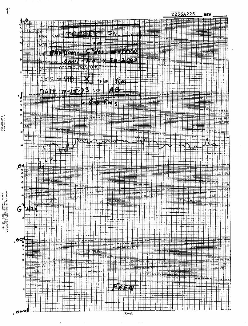
RANDOM VIBRATION
Procedure
A random vibration equal to the total G level utilized onthe LEM and Skylab was impressed on the switches. Period ofapplication is 2 minutes.
1150-2000 Hz 20-2000 Hz .02 gr/Hz
3-1
F4202-1 2/72

THE SINGERCOMPANYKEARFOTT DIVISION Y256A226 REV.
Switches Tested
Pushbutton
Toggle
Rotary Switch
RESULTS
All switches functioned throughout the random vibration.The pushbutton normally open remained in the normally openstate, the toggle maintained in a closed switch positionremained in that state without interruption and the rotaryswitch set at position 5 remained closed in that positionwith all other positions normally open. The graphs on thefollowing pages visually depict the vibration levelsapplied in the during the test.
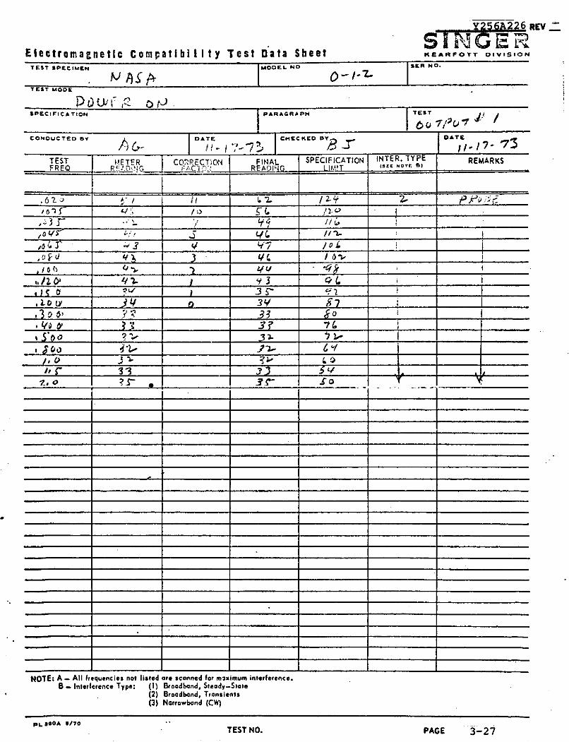
EMI TESTS
EMI tests were conducted on the double pole, single pole and thepotentiometer in accordance with MIL-STD-461. The tests per-formed were CE01, CE03 and CS06. CE01 and CE03 were preformedon every lead of the device under test. CS06 was preformed onall power leads with the spike equal to 50% of the nominal linevoltage.
RESULTS
The results of the CE01 & CE03 tests are contained in theattached data. Emissions for all devices were within themax specification limit. All devices operated successfullyduring the CS06 tests.
3-2
F4202.1 2/72

Y256A226 REV
it
iji i :t
a "+i i'tt , i
i j j
41: 71T -IX
~Ut
,O 1 R
t ±- _ - - __-1 T_ 4: - - - --- ii-1 ii I ;
"7~
G A- -1---F ir'
4 rf ; : iT4 !T i
-1 -
lizi +flL I 11 TI 1r1-Tr L r - 1I i... . : J .. . . il
Imw .j ' j i | i t
-4 r -t t-JNOO 1
J tf
-:t 1 - 1 f 1 - 1
i- l it s.. ---
_4 All I. 4i f t--- - -- 1
3-3

Y256A226 RE ......
7 - ---r -: . i i4~4
- t. -A 1 4
Ot 11i ELI j f f it
tt "'d... ... ... ... t ~~
. -i
4- -t Vii
6"7 T-ii
-4
tt
Ss ----i------ - i
M i =WCt
.00
S 6 -- - -Ik.o .I
2 1 j-i- ~ l
if j i -- tt-ii oil -i I L A-
44
itIt
3+ 1 H
3-4

NO
15T
-
L412
GR
AP
H
PA
PE
R
VIS
IGR
AP
H
S.M
I-L
OG
AR
ITH
iC
M
AD
E IN
U
5
A
4
CY
CL
ES
X
12 D
IVIS
ION
S
PE
R
INC
H
o0
0
*o
M
W
-
.la
* *
* *
,I
i I
--!
--
-I
I I
L
-.
.
i I M
II
NO
15T
-
L4
12
G
RA
PH
P
AP
ER
V
ISIG
RA
PH
S E
MI
-LO
GA
RIT
HM
IC
,AD
E
IN U
S
A
41 C
YC
LE
SS
X 12 C
VIS
ION
S
PE
R
INC
H
U 1
t : 1
1
1 il!
Il
l H
it
;I
lIl
l l
l
IT
-I
I TI M
II
I I'I.
; I
:'""
" ""
'""U
r T
~~
~~
~tr
r~ti
~
~ ~
;/
.Ii
ITlm
:!
jl
lli~
:1:1
:11
i
1*
--
-I ~
~-r
Iil
iii
I II
ili
I H
H
tIi
i I
II
II
-
I 1.-
4
Il i
i
I T
L
L-4
II !
1
I I.
II.
l
-4,~
WWp
il
l ti
ll
LH
I
M 0
T
UFF
T
TI
11'
i.1~
il
1
I I
II
*i
i til
I
'iim
ilill]
til
l
IIli
il
I :I
Ll!
;liI
1'i
\'iI
-Ci
" ""
""
'' ""
~~
~iC
i
+
t tt
n
-ff~
I.111
1
1 It
il
I U
A
flu
LIU
r'-1
Iii!
.l!
ll!I
lill
Il
ilil
ll
I I
II
II
I I,
t~~
t~
t t~
t tt
tm
~it
; /
tr
E,
I I
i4.
#1 1
.1:
IIi
II
II
II
4 1
1 1a
'I
ION
~i
ii17+
11
Hil
i
I i
I W
::
lil
l ll
till
I
I( l
lil
il
llil
l il
I I
M
l H
I i
ll
l 1 1
;i~
lln
il
ii
iIi
)/I1
i
iiIl
ll~
llll
~li
ll
iIi
1111111!1
1111i
I:I
ItI
II
II
Il~
r~uulr
uuur+
u
O
-T
H
it''i
' I
~ -;
-tt+
tttt
mr~
t~tt
t i~
I
LE
L
UL
I
,II!
-
-~-e
i

NO
. 15
T -
L41
2 G
RA
PH
P
AP
ER
V
ISIG
RA
PH
5 C
MI -
LO
GA
RIT
HM
IC
MA
DE
IN
U S
A
4
CY
CL
ES
X
12 D
IVIS
ION
S
PE
R
INC
H
co 0
-d
am
77N
L24
f++
, F
w0
I II
:
LW
M
FM
IlF
11
LI.
7u
l-i
I I
U
-~I
-r7I
-T
,
<+
4:
IIIff
nrm
~T
T;
: Ilr
l l
II
J,.
II
iI
I ~I
I ',
-II
I'
II
'II
-"""
L"
IIL
UY
~Y
~
II
*"-~l4
i41IP
IQ
V I
II

NO
15T
-
L4
12
G
RA
PH
P
AP
ER
V
ISI
RA
PH
.
S E
MI-
LO
GA
P
TH
MIC
M
AD
E N U
S
A.
4 C
YC
LE
S X
12
ON
S
PE
R I
NC
H
0 '0
~_4
I -
1
-I
M-L
ID
I1
-:*
ftIi
I
I I
.1
1
ON
1 1
T
I II
II
II
N 1
I4
+
i. IiL
I
I'
17
;o,
1I
I :
t~M
__F
4
4H
-
7
.....
1-.,.
.....

O
i5T
-
L4
12
G
RA
PH
P
AP
ER
V
ISIG
RA
PH
s
MI.
LO
GA
RIT
HM
IC
/AD
E
IN
U S
*
4 C
YC
LE
S
X 1
2 D
IVIS
ION
S
PE
R I
NC
H
t b
W
a qI
w
0 qw
W
(a
4
01
0 -4
M
.0
1111
1111
11,
4T
+
-t
I I
I .I
N
.11
I I
L
I-
.1
I I
-
I -
IIII
S---
r I
-4-
--(j
1
"LW
LL
YY
I II
UC
rU
rr[j
!IT
~j
~ ~j
[llii
I
Ill
iit
I I
in
-I
III
:111:
I'
.-~
l Ii
l
-Ill
~l~
llll
Ii
l ~l
l~ll I
I -
-~;t
e~
t~
t~tt
~tk
ti
tt~
t I
i!
II
i;gi
1 T
.
I .
Il.-
.-
I -
I ti
Il
IL -
TI4
Ii
i i
i i
IIi
-I
4 ,
I I
I.N
I I
7I
7'~
+,
1h
i M
111
-t
I l l
l
l-
I -
i-
I I
.. I
I -
M
I I
---
I
~
IC
--,
li
lt
lil
lt
Hit
iiii
i I
4 1
t ill
is
li
lt l
ilt I
ll! l
ilt
I I I
L
I I
-II
*I
-
lilt
I I
-4
I !
1
I I
tilI
H
i I'l
Il I1
-il
" 4
A
1 T
,
+ -~
"
I -
II
411
7
m
l 111
I-
4-
HI T
i-
-'
m
II
I ;
-,
1 l
l !
1 1
1 1 !
1 1
t
l
i I
It
11 1
1
44 ,
+1
HIi
ii
IM
i
It~
-L
L
_L
-
~ H
II
:il
---I
-ilk
II
Lhi
J
-44
4T
TI
I ~~
I

S
EI
LG
A~
TH
FC
VIS
IGR
AP
H
IN
O i5T -
L4t2
G
RA
PH
P
AP
ER
V|SI* R
SAH
5E
1L
Oi '
RIT
M
IC
(s.,
r ,.
O R
'
(.
....
(
S 00T
i
F
I
tt
--
144
--
-''
FI!
-
F
I '
i4- -'F
----
,'
'--
--C
-
I '
II
--
i
iiii
IF'
F
F
F
F
' ,.
F
F"
" '
."L
~ +
t t-
r~rf
i~~
T
i
-F
F
F
'''
F
F'.
F~
F
IFF
F
Ftt
F
~
F
i~~~
~ ~ ~
~ ~
F
, F
F
F
F
IF
' '!"
U
L
-~ +
i
'c~-
+
r ~
t ~ r
r -
m
r r~
m r ~ il
I
i 1
I 1
1 1
11 I
i I
I !
ll lt
l l
lll!
lL
L
LL
t t~
t t
j~ i
~~ t ~ t
r^nr
Ti
~F
i F
'F
---
--.m
-m~n
inm
ri
- i
i ;i
ll
I I
I i
i II
IIII
1II1
!1II
II i
i l
il I
IIII
III1
IIII
i~
ttft~
rt-t~
rtt
t rt
TT
~i~l
Tj~
jrm
0 IQ
~Z7I
~L74
'~
.,'
' F

Y25bA *z y fa V
Electromagnetic Compatibi lity Test Data Sheet KEARFOTT DIVISION
TEST s ECIMEN MODL. NO SER NO.
TEST MODE
PECIICATN PARAGRAPN
TEST
CONDUCTED DATE CHECKED BY DATE
., 73
TEST M.;ETER CC .ECTIO;I itl L SPEC IF ICATION INTER. TYPE REMARKS
T"M l'.z CTp. ,4 .,..,_ . t-./
.a'• H_ I __ _ I /2V ( :
, . -- -
.o_3 _ ______- -1--
,o- I f" I
____ ___ 3 -_ __
.o 3'3
4,) 33 1 St4/
1 30 o,
_ _ __
13 _. ;_ _D_
,3 3*
(2) Broadband, Tr sients
(3) Narrowband (CW)
__.___ 3/ 1 1 PG
NOTE: A - All frequencies not listed ore sconned for maoxrnmum Prterte1enc.
B- Interference Type: (1) BrocaSand, Steady-Stlte(2) Brocdand, Tr asiets(3) Norowband (CW)
pL9BO* S/IC TEST NO. PAGE 3-11

Y2 bIAL 4bEV
Electromagnetic Compatibility Test Data Sheet KEARFOTT DIVISION
TEST SPECIMEN IMODEL NO SER NO.
1O 7 E/J -, / /0o jLFF 77A/ jSETEST MODE
SPECIFICAT ON PARAGRAPM TEST-/ o v i -CCONDUCTED BY DATE CHECKED BY DATE
S1-2 -- ) 3 H/J //- Zo-~)TEST I ETER ICC7RECTION 'FINAL SPECIFICATION INTER. TYPE REMARKSFREO E E~:'G FACTO' READ!, !.lT (sMC IOTT ea
. ,o / . /L..,0," '# ! /. O z (. " I " I 7_
o3 -3 " 6 7_ 4 /,__O_ T T / ,- I
o 73 ( 3/ -1.50 3 -3w- __ _7 _ /
1.O,_ 31 3 7 /
0. _ _o 3 /
,> Jo •(o /_._o _ _ _o i /
30 .0 __ f / *
NOTE: A - All frequencies not listed are scanned IVr maximum interference.
B - Interference Type: (1) Broodband, Steody-State(2) Broadband, Transients(3) Narrowband (CW)
pL.390A 9/70 TEST NO. PAGE -T2
__ _ _ __ __ __ _ _ _ _ _ _ __ _ _ _ _ _
______ I __ _ ;'l ____________ /c ______________ ___axmu itofre c
--lt;--rn c _ye /1 _odad ~ed-l

Y256A226 trEV
SINGERElectromagnctic Compatibility Test Data Sheet KEARF OTT DIVISION
TEST SPECIMEN MODEL NO SE NO.
.6 7-F 7 / o 7f , 7TEST MODE
0AA J ile T
AET
SPECIFICATION PARAGRAPH
CONDUCTED By 4 . 0 A CHECKED Y DATE z
TEST ' TER CORRECTION FINAL SPECIFICATION INTER. TYPE REMARKS
FREQ oE')E FACC I E A.IN LI sC No? B)
0 o /2
7 -73 /
.o 1 /
S3 3 7 /2 7
SO 3 3'o -- //o 33. t_ /
/I ,u 3 o 3 J330 ,
30.o 3 ° 3" // a- , a 3 .i 0 -
.o 3 _ I _..
NOTE: A- All frequencies not listed are scanned for maximum interference.
6 - Interference Type: (1) Foadband, Steady-State
(2) Broadband, Transients(3) Narrowbnd (CW)
SESeoA eo T O. PAGE 3-13

. vy9 E226 RIEV
Electronagnetic Compatibi t it y Test Dato Sheet KEARFOTT DIVISIO
TEST SPECIMEN MODEL NO SER NO.
pot.7 t/J 7, 7c7 f/f /VTEST MODE
SPECIFICATION PARARAPH IT
CONDUCTED BY DATE CHECKED BY
DATE
A , L- ,7 1, /-z - 7 Z
TEST ?"TFR CO 7"1 CT IO1 FINAL SPECIFICATION jITRTYPE REMARKS
FREq P ._;_, E IC iO
_, ._..
.--Q-- --
,o /"o /_ /: '_ __ __ _ __9-7_
/2j 01 (4 9
o. 0 &o 7z
So 0* 3-7 3 /7 /
,/ 30 30 ! I
o I /7,- m 3 /
__ ,_._ _ __ -o - .3 o /
(3) Norrow 3bnd (C)
.o TEST NO. PAGE 3
-, 0. 30 v __
,__ , o_ _ 1 __ _ __.'
NOTE: A - All Irequencies not lisled are scanned for mainum interference.B - Intererence Type: (1) Broadband, Steady-State
(2) Broadband, Transients(3) Norrowbond (CW)
PL 390A 0/10 . TEST NO. PAGE 3-14

Electromagnetic Compatibi I ity Test Data Sheet KEARFOtT OVISION
TEST SPECIMEN 4 MODEL NO SER NO.
TEST MOOE
PECIFICATION PARAGRAPH TEST
CONDUCTED BY DATE CHECKED OY DATE
TEST 1TER CCOECTION FINAL SPECIFICATION INTER. TYPE REMARKSFREOQ __._G F,CT.0__R E,-DN_ _ _ MIT sEM RorS e, i' . C /. (SE,,C 0 ,)
FK C T C
___ 0 _______ C 3 __
11
NOTE: A - All frequencies not listed are scanned for maximum interference.B - Interference Type: (1) Broadband, Steady-State
(2) Broadbcnd, Transients(3) Narrowband (CW)
pL30A 9/70TEST NO. PAGE 3-15TEST NO. PAGE 3-15

J X 10 To riw INCw 4I O703
SI .. 1L . 1 1 K I.. S
i ! ! : i i tIi - !r.I -iI:i' t / 11i iIi.i:i i i '0i a 77-7 __
, 1 I + i i i "
S Kli 'i , i II - 1I' I !-N i - - Ii t : +I I I ii _ 1
ii I ii 21 I - -I
• ..i i i , , ' i -t 1 + - i i "
' i I- £ --i
Si -I i I .i.... 1
P4-~~~~~~~~~~~ I 'i , :i: iii\iiii1Iiii :-
Ii I i l - i 'iiI I I i . , i , I , : i I I i I !
ITI, i ! IiII '_ _
' ' : : .. I I,
. ' ' i l i i : I i i' :
• t ii;' i 'i 1. l I: Ii' : : j 1 .. i i i -i !t ! I + ~
.. .. ,II ! -Il ... ii.i-1 ,
4 K 11
" I , , i + i i , + . i : i i: , it ,' i i ;i li - i i-! :
,1._ -'!. i ; ; I !t1i ~ 4P /"Yj~ /
, I • I iI j . If i ti\ IIii~
L lj
: ' I 1 j ~l i- i i 1 -i 1 I.2. qI-. jI .0 1
av 11 il i ff
?' '-T -71 .71 L
i IA i 1 1- 1 J, I- I I i i I
3 06-- 1 ILL I

" ,' )0 It' i Iif: INCH 40 0703
oKr..l rI. a I sqt" Co. M11,- 'TI -L' S
.'" " I F I 1
0 0 ---- ~- uv- f -- r r T ~ n TIi1 'I A i 6'/?d4. I' 'i .. . ii i . .. .... ... .-- -. -I ,~ -I , 1- ,- -r t ,,
70 Iiiij~I iiiiiI(;f dCyIB/pI t
il II IiI I I-
1-7!!- I A!
. 1 " - , . 1 i i I , I #.D 1#
ji
PI: , 1 _ - 1 1 ".
', :, + i ' I .' . ': i i 1V .6
,9O L I* . : I ,i " I I
X .l .. .. .'I' I 1 It It " "i : '. " I: iI1i 1 . 1 jI1~IijO q C~~[ ; i I ! i i i I .i
I "
: I -
!
: i _ i i /~, ; I i'' i l l li I 1 '1
I I
1T
IHi ' I -j LI
- I/ I : , ! ; 1 : Ri: I !
.. .. _+.. . .... . . . .
r + I i i I . '
I -i1:, : I +II I ! "1 :i ', " " : i t s : ' + "l
I: !-, ! , ills 4il
A j I . f .
"I ' J &'
101 v
*= A ; t , " ; : C A• , .v ; _ i , t I-i
:: ^ . ' - ' ,. i ._; : _.. .....I." ' ' .1 i .I i i- , ,a. l' i i+I1 ' -:

4!; 10
M.' M -1 f.' l .'1.101 1 11N I ~'FRI CO.
i~it5 5 II- -Is -L i
T-1-
J +
1A~I I- 5
iii I Li i.- 4- Ic~ I-.I.-
L . T
IiJ
t! l
SI i ~*4 jI t:j.I..: 1 U]**Iivii ii.L 1i~itE t~1
dI 'E 9 Kb- Ww w/ L~i I
: :I i: -J,
I-1 -t ~1L.._L..;IJl01 ''x
: i i! I . j~l I. 44

i, 1t ro THr 14C H 46-0703
Krurrr'. I w C O- MI co. -4G I A
J i
LK -' _ lI I'
1I H V
Qlil-I:I.Li 'i
A 0 L
I I jz~ I iI ~ I
11KV I 74; resrt-i
IL ELVG.-L liii
3I Od1 54C/vr t2C.A X
I 1111 1.i
*i Il K.
II; I ' '
I I .I... 1- II ;.. -IIi -i i ij(!sj- 1 f, ;-1 iI i I I i ; -
W!.. I I i'i1i'ti-1I .aa
2- $4 g /0 1.11~;' jjj I 9 j.9L.jijj~3 .3zL13EL.. /~

Y256A226
SINGE LCElectromagnetic Compatibi lity Test Data Sheet KEARFOTT OVISIONTEST SPECIMEN
M ODEL NO SER NO.
TEST MODE
SPECIFICATION PARAGRAPH TEST
CONDUCTED BY DATE / CHECKED BY AT
TEST M~TER CRECTI ON FINAL SPECIFICATION INTER. TYPE REMARKSFREQ PE.N FI- -TR REArDIG LIIT .r wNO B)
/6 ? /4 'Z.G 3 /,Z2 L, 22 2 0 " 3 /
NOTE: A - All frequencies not listed are scorned for maximum interference.8 - Interference Type: (1) Broadband, Steady-State
(2) Broadband, Transients(3) Narrowband (CW)
.PL$SOA 9/70
TEST NO. PAGE 3-20.

Y25I 1 4 E RE
Electromagnetic Compatibility Test Data Sheet KEARFOTT DIVISION
TEST SPECIMEN MODEL NO SER NO.
TEST MOOE
SPECIFICATION PARAGRA*PH EsT
I C ICONDUCTED BY D CHECKED BY DA/II ° /'
NOTE: A All frequncies not listed are scanned for maximum interference.
TEST ETER CORECTIN FINAL SPECIFICATION INTER. TYPE REMARKSFREq tEAD Cj FACTC R, NGLT_,-___
NOTE: A - All frequencies not listed are scanned for maximum interlerence.B - Interference Type: (1) roodband, Steady-Stole
(2) Broadband, Transients(3) Narrowband (CW)
P- sOOA 9/10 TEST NO. PAGE 3-2.

Y256A226 REV
SINGEElectromagnetic CompatibI lity Test Data Sheet ,.,KAROT tvs.oNTEST SPECIMEN MODEL. NO SER NO.
TEST MODE
SPECIFICATION PARAGRAPH TEST
CONDUCTED BY DATE CHCKED BY DATE_o _o _____ __,__, _ /1-/- 'y ,
TEST METER CORRECTIONI FINAL SPECIFICATION INTER. TYPE REMARKSFREQ PE NO FACTOr READING I IMIT I se .oTE B
. C- S-i 2 c - po /.?/0,7 2.. o __ _1 L '12 - 30 .I2.0 2 0 2L O I 3 _
NOTE: A - All frequencies not listed are scanned for maximum interference.B - Interference Type: (1) Bioadband, Steady-State
(2) Broadband, Transients(3) Narrowband (CW)
PL&900A 9/70TEST NO. PAGE 3-'2

Electromagnetic Compatibi lity Test Data Sheet KEARFOTT DIVISION
TEST SPECIMEN ' MODEL NO SER NO.
TEST MODL
SPECIFICATION PARAGRAPH TEST
CONDUCTED By - oAT,/ CHECKED BY OATE
TEST Y TER COORECTION FINAL SPECIFICATION INTER. TYP REMARKSFREQ PE DlG FACTOR READING I IMIT o B
A - 0 -
/o.7 ___.-____ 0__ __ _ _,/9.-) _ l o 2./ ___ _ //
Ii
NOTE: A - All freauencies not listed are scanned for maximum interference.6 - Interference Type: (1) Broadband, Steady-State
(2) Broadband, Transients(3) Norrowbond (CW)
.pLSSA 0/70 TEST NO. PAGE 3-23

Electromagnetic Compatibility Test Data Sheet KEARFOTT DIVISION
TEST SPECIMEN MODEL NO ISR NO.
TEST MODE
C ."; A o /JSPECIICATION PARAGRAPH TEST
2t/' Di.CONDUCTED BY DATE CHECKED BY DATE
P./, ,- 17-73 1. '7 //- /7- 3
TEST MEER COR RECTION FINAL SPECIFICATION INTER. TYPE REMARKSFREQ RE ING FACTOR READING LIMIT sct NoTE 6)
' 2 C P. k /7 / 3"
0, q6 3 V 22 //
1. o 3o I /1 QA,6 o 3o .3o _o
. o 3 /0 ___- _S. 30 930 __ jj - - _ _r "
_,_ _ 30 0 Jo _
-ou 30 3 1 76,Soo 'LJ
/3~ S 3 S
J.0 30 ,
5 n tro _cTe (____t_-t
6,630 37
3 0 3o
g.3 7 30 7 __ 1
NOTE: A - All frequencies not listed or. scanned for maximum interference.8 - Interference Type: (1) Broadband, Steady-State
(2) Broadband, Transients(3) Norrowband (CW)
TEST NO. PAGE 3-24

Y Y256A226 REV
SINGE RElectromagnetic Compatibi lity Test Data Sheet KEARFOTT oIVISION
TEST SPECIMCN HODELNO SER NO.
TEST MODE
SPECIFICATION PARAGRAPH TEST
COUCT DTE CeHECKEOD BY DATE
TEST I ETER CORRECTICN FINAL SPECIFICATION INTER. TYPE REMARKS
FREQ PE; FACT REAOI:G LT , C 1o- )
,o7 __ _ 7_ _ - -;
,I I/ I
NOTE: A - All frequencies not listed are scanned for maximum interference.
8 - Interference Type: (1) .,oadband, Steady-State(2) Broadband, Transients(3) Narrowband (CW)
pLLo3 o T N. PAGE /3-70
5
TFCT Nn. PAGE 3-
TF~T Mn, PAGE 3-25 1

Y256A226 REV .
SINGEElectromagnetic Compatibi lit y Test Data Sheet KEARFOTT DIVISION
TEST SPECIME' MODEL NO SER NO.
TEST MODE
Po wc: o:SPECIFICATION PARAGRAPH TEST
o 7 Po /'. O -7"CONDUCTED BY DATE CHECKED BY DATE 7
_,_, _-_J' _ _ /- 7_
TEST METER CORPECTION FINAL SPECIFICATION INTER. TYPE REMARKSFREQ PE,;G FCT O READING LIMIT (SE No~r B)
.S I, -7 __ _ _ _ _ _ _ ,_ _______: -
,c, 3Y 7 V/ //6SV 3 5 3q _ /_3 Y_
,100 To
,-7
2, o I
'I F' _o 3
.6e_ _0
12,o 30~ 2
., ,.. o . 3 ~.
B - Interference Type: (1) B oadband, Steady-State
(2) Broadband, Transients(3) Narrowband (CW)
p,.l0A 9/70 T " TEST NO. PAGE 3-26
Electromagnetic Compatibility Test Data Sheet KEAROTT DIVISION
TEST SPECIMEN MODEL NO SER NO.
TEST MODE
SPECIFICATION PARAGRAPH TEST
CONOUCTED BY DATE CHECKED BY DATE
TEST METER CORRECTION FINAL SPECIFICATION INTER. TYPE REMARKS
.*o -I _ __ _ __
,u3 o _? __3 3 _o
,61 -? 3 _ ".
NOTE: A. All frequencies not listed are sc3nned for mximum interference,
(3) Narrowband (CW)
S-_0A 9/703
TEST NO. PAGE 3273 ./ _ _T \1
NOTE: A - All frequencies not listed ar, scanned for m2Aimum interference.B - Interference Type: (1) &oodband, Steady-State
(2) Broadband, Transients(3) Norrowband (CW)
TEST NO. PAGE 3-27

Y25iA226 REV
SINGEElectromagnetic Compatibi lity Test Data Sheet KEARFOTT DIVISION
TEST SPECIMEN M ODEL NO SER NO.
AI /)A 5; -TEST MODE
SPECIFICATION PARAGRAPH TEST
CONDUCTED BY DATE CHECKED BY DATE
TEST I 'ETER CORRECTION FINAL SPECIFICATION INTER. TYPE REMARKSFREQ I _G , .CT READG IIT
i , '.4:A ,/' , C. .'h...'' . .K cF/b A
0 -7 C _
St' 3 3 5_
,o6 , / _.,_ _6 '2-
SI i _
X ,- 7 03 7 S 7
(2) Beoadband, Transients(3) Narrowband (CW)
o TEST N. PAGE /3-0

SY 2 56A226ftEV
Electromagnetic Compatibility Test Data Sheet ,A OTT DIVISION.
TEST SPECIMEN MOoEL NO SER NO.
TEST MOoD
SPECIFICATION PARAGRAPH TEST
/0, CCONDUCTED BY A DATE/. CHECKED DATE
TEST kCT7ER CORRECTION FINAL SPECIFICATION INTER. TYPE REMARKSFPEQ FACTOR READING LI.ilT It 1 or- 8)a
.. u..... /I III A,o _ ? _ o . _ ___ o_ _ _ _
r 37 S 37 , ;
*100 3 o _ _________
, yoI / IV
a,9 7 7o -
, po o )0o i
* -0 - -3o,o 4 1 33 __ _
2, o 30
31o 31 i___
. 50 1 _o __ I __ _, I _
So. o e .6,
___o 33 33
NOTE: A - All frequencies not listed ore scanned for maximum interference.B - Interference Type: (1) Broadband,.Steady-Staote
(2) Broadband, Transients(3) Narrowbond (CW)
PI.s90A 9/70TEST NO. PAGE 3-29

Y256A226 REV
SINGEElectromagnetic Compatibility Test Data Sheet W , IOTT oDIVISIOTEST SPECIMEN MOOEL NO SER NO.
R A A - I - 2TEST Moo
P 0 w it iJSPECIFICATION PARAGRAPH TEST
CONOUCTED By DATE CHECKED BY . DATET,AC //-/7-"3 1. //-17-27?
TEST METER CORRECTION FINAL SPECIFICATION INTER. TYPE REMARKSFREQ PEA!NG FACTQO READING L"!T w1SC NOTY 8)
_ _ I _ _ : _ _ _ _ I _ _ _ _ _ _ _ _ _ _
ooA W30 S
• ,1 o _ / _ _ _ _ _ _ I __
, ro o 3" 3 . E.
, 0o a3Y' 3Y _ _ _"_ _
-'- J 2_ _ - . 37. _ ,__ __ ._
NOTE: A - All frequencies not listed are scanned for maximum interferetnce.B - Interference Type: (1) Broadband, Steady-State
(2) Broadband, Transse ts(3) Norrowbond (CW)
.PL.IIOA /70T
TEST NO* PAGE -3-3 0

Y256A226 REV -
SINkGERElectromagnetic Compatibility Test Data Sheet KEARFOTT DIVISION
TEST SPECIMEN MODEL. NO TER NO.
TEST MODE
Po -. t ,dSPECIFICATION PARAGRAPH TEST
So0 -rRor '2CONDUCTED BY DATE CHECKED BY DATE
. ;-. 173 a . /-1/7-73
TEST 1 ETER CORRECTION FINAL SPECIFICATION INTER. TYPE REMARKSFREO ' FACT., READING L_ _ IT _ _ _ _mor_ B
L r ' ' C P A"
. , ,-_ _ _ _ _ _3 I '7- __ _ _ _ _.__ , -
, 6,)4 / -6
V3 • 3 -,o
./. -.'1 -- 7_ t , 3 3 0_ I _
o.o __._0_ 30 _ _
TEST NO. PAGE 3-31
pL 3OA 0/70TEST NO. PAGE 3-31

Y256A2 REV
Electromagnetic Compatibi lity Test Data Sheet KEARFOTT OVISION
TEST SPECIMEN MODEL NO
1 SER NstdO*TEST MODE
SPECIFICATION PARAGRAPH TESTS 1/,/3 ,e. L/,j,
CONDUCTED BY DA 3E/ CHECKED BY DATE/ 7
A. G- I"T1 E//7 1-7 3 1. IT I /TEST METER CORRECTION FINAL SPECIFICATION INTER. TYPE REMARKSFREQ EDE-!GA FACTCP 1 READING LIMIT ISCE NoT B
,*" ' i " " ', I 4 p,/ ,:,,__5 _ i _ / . / /
, o6b Jo u 3Y t, o_ _ ___ o i _ _ 33 1 o_ __
,_ ,_ _ L 3- / 1 9 -i
,o 3 3 3 Y_ o_ o 3" / 3_o i _
, .0 . I i ;730.300 _ _ _ _ _ ______________
. , .__,, .__ _ 1 74 _ _I
), j Y Broo.___ ___ Tr _ __3
) . .0 f hr ) -b
6.4- p, _ _
C _ -1- _ _ 0
TS30 3 0G
_ _ _. 3,:) 3 c>' V
NOTE: A - All frequencies not listed are scanned for maxirnmum interference.8 - Interference Type: V(1) Broadboand, Steady-State
(2) r&odband, TransientsO3) Noao wband (CW)
pLISoA 9/70TEST NO. PAGE 3-32

Y256A 2 6 REv
SI GERElectromagnetic Compatibility Test Data Sheet KEARFOTT DIVISION
TEST SPECIMEN MODEL NO SER NO.
TEST MODE
SPECIFICATION ,PAAGRAP TESTO C 7-r r
CONDUCTED BY DATE CHECKED BY DATE
TEST METER CORRECTION FINAL SPECIFICATION INTER. TYPE REMARKSFRE PE I FACTR RF. C No LI1MT fs5EE OT 8
_ _ _3 ? i 3 /,o_ _ _'_ ,__ _ la / .. ,_
110 39 E 31 //t, 3I 3, , I
,_ o _ _0 _ _ 3 , _ _ _ _ _
lo _30 31 4
,_ _ _ o3 _o -7_
, _ oo 3o I - 30 7L
/, 0 730 3 _ _
2,(2) odband, Transints
__ _ _ _ (I3o v - _
(3) Norrowband (CW)
.p6l90A 9/70 TEST NO. PAGE 3- 33
>0~ __ _ __ _ __ _ __ _ __ _ ___ ___ I - ____ ____ _
___ __ __ __ __ _ __ _ _ I __ __ 1) __ __ __ _ __ _ _ _ __ _ _ _ _ _

Electromagnetic Compatibi lit y Test Data Sheet KEAR OTT OVISION
-TEST SPECIMEN IODEL NO $tR NO.
TEST Moo-
Po f/ ivSPECIFICATION PARIAGRAPM TEST
S1 /2 U, D.C . //vI
CONDUCTED BY DATE CHECKED BY DIATE
_A6- 1,-,7-73 ! !_ 7/,-/73
TEST METER CORRECTION FINAL SPECIFICATION INTER. TYPE REMARKSFREQ PEiG FACTOR READING ILMIT (sEc NOTt R K
•oVs 3 -5 3 i ! /,
.o6. 2 "' /o'
.03S L L/ 0
I'S 3y 11 _-
S 30 3 0 3 47 7
/. -.,'3-4 t .
_ .____ 3-, L_ _ 3 72 _ _'_ _
_ ,_ o 30 . 30 _ 4/- _3
_ /_ __7 3 3< J: &L( J 31 i0 _ _
3. -7 3 3r 7371
/1_0 30 y 21 3 1 4.
_ _ _s_ _ o 30
NOTE: A - All frequencies not listed ere scanned for maximum interference.8 - Interference Type: _(_) Broadband, Steady-State
(2) Broadband, Transients
(3) Norrowbond (CW)
TEST NO. PAGE 3-34

.Y256A226 REV
SINGE iElectromagnetic Compatibi lit y Test Data Sheet KEARFOTT DIVISION
TEST SPECIMEN IMODEL NO ISER NO.
J ) J AI /TEST MODE
SPECIFICATION PARAGRAPH TEST
/2.,o V. D.C "
CONDUCTED BY DATC CHECKED DY DATE / /
TEST LCTER CORRECTION FINAL SPECIFICATION INTER. TYPE REMARKSFREQ _P _ C REA)l IL IT (s Norte a
;-3.___/ _ 0 _ _ __7-__ 3 ___ ,_______/ 4 0 I 0 f L- o 3 ,
NOTE: A - All frequencies not listed are scOnned for maximum interference.B - Interference Type: (1) Broadbond, Steady-State
(2) B&oodband, Transients(3) Narrowband (CW)
PLi90A /170TEST NO. PAGE 3-35

.... Y256A226 REV Z
SINGEElectromagnetic Compatibility Test Data Sheet KEARFOTT DIVISION
TEST SPECIMEN MODEL. NO SER NO.
0-i-/TEST MODE
Po w(le o . -SPECIFICATION PARAGRAPH EST
CONDUCTED oY DATE CHECKED BY DATE
A &- I 1 73
TEST METER CORRECTION FINAL SPECIFICATION INTER.TYPE REMARKS
FREQ Pj DIN F.-,CfOR READING L___T sI
1 os/Ji . 'i .. .: . C.2 ,
/F. o 3
________________________ a-
NOTE: A - All Frequencies not listed are scanned for maximum interference.B - Interference Type: (1) Broadbond, Steady-State
(2) Broadband, Transients
(3) Narrowband (CW)
L 5o00A /70o TEST NO. PAGE 3-36

SY256A226 REV
Electromagnetic Compatibi lity Test Data Sheet eXARoTT DIVISION
TEST SPECIMEN MODEL NO SER NO.
TEST MODE
SPECIFICATION PARAGRAP TEST
CONDUCTED BY DATE/ CHECKED Y T AT
TEST M TER CORRECTION I FINAL SPECIFICATION INTER. TYPE REMARKSFREQ R DI NG FACTCR REAING IT . oTr
___ R E AN Lm, o Lo 3 .
L ------ -
NOTE: A - All frequencies not listed are scanned for maximum interference.8 - Interference Type: (1) Broodband, Steady-State
(2) Broadband, Transients(3) Norrowband (CW)
TEST NO. PAGE 3-37
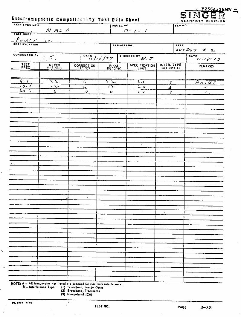
Y256A226REV *
Electromagnetic Compatibility Test Data Sheet KEARFOTT OVISIONTEST SPECIMEN IMODEL NO SER NO.
_ . A/,,.; A , -, /- /TEST MODE
SPECIFICATION PARAGRAPH TEST
* I *.* - / 2 .CONDUCTED BY , DATE CHECKED BY DATE
TEST M(TE CORRECTION FINAL SPECIFICATION INTER. TYPE REMARKS,-FREQ P -... ; F;.C r ,R RE - ING LIMIT fs e N = N s 1)
Z-, __L ___ 3 /D___ U
.,__I __ / " _____E NO..- PAGE3.3 3,'
NOTE: A - All frequencies not listed are scanned for maximum interference.8 - Interference Type: (1) Broadband, Steady-Stat.
(2) Broadband, Transients(3) Norrowband (CW)
PL S90A 9/70
TEST NO. PAGE 3-38

* I) II. 1 iG 07A. .
Mit -$'To;CI n~11~~f i. ;- i +,J H.+ +:' ..
i'*ii HiilI '' ' I i l. I .'. -1 -. I. ut'00 - m-
'" -i II ii i 1 I II- i iiri iii
I ''IIF-. --i --- ....
+'T I "I I. 'I
j i.....i-.i i- ' ij(j ii ir i +~ t i / r JS I/ I " i
" i ri -
I I i1 : TK $,C 70 I ' (.,
" ~i: I.v I I I ,. 71 l" .... :
.- .. I, .I* ' i +, i' ' . " - - I 1I /11,
+"1 1~ ; :+ "' ... i i
I i I. I.. I I
+ i . + i i t " L : + -
I i' i . _ I i i , I . i i ,t iI I I 'K . ' I -
"+ +j
i'l I! i l ; , I
L I 44 1 i I '4.H1+ L
LJi
".+i ' 6,
. .
30,o 2M-
.= C- 9 K//
I ii- i i1 ; i ' +ii i 1 t i--
t i , " i : , ; ! !i:j j - .i ._ : I
i -... ; • I --- i i iI ' . .. .~ ~ . -ti • I
+ .~~I ... ++ t-1 .+r- ,3 ; i t : + ' - j. ' ! + . i ; , i i ' I
;Q i : I- i i : . : !i t i
,i + i l i ,i , ' , , : i -:
+ + ; iI+ j+ I " i -I i :[! t .1.... iii + + + + +t i + + ' * + +I+ : i i : I+ i ! -L j , ....-j~! ,, , .+ : . i ...... , ., , It- j~. t I'" ! " : ! + i ' ' .: : : + : * ! i .i + '
'i t " .i- I i i
I ;I i i. r, i : ... t :1ti i i. -.. . + , . . . . I +. i . i _. i ii
!i :... + *+ , ' : : ' ++ +++ ,: !i i ++ i iiI -,- i+i : u I i It1 -i+.r it1- ti i, i i- ii ii -I ii iiIi ;1 ii i-.i-i-I lrJ : i i~
. : +" , + i : : ' It ii -.... .I +I ' i i i i,.l++_Lt 1-ii i * i-1i - +-l-' _,,. .~i , .. ... + _ ,l- ,~-I , i , -s oo .. .... .z ...... . "/ i s . ,,z
3'' ' '9 . K//

x. >: 10 10 1ir°
Ii #4 , C .
I. - lrl. I 1AI I .
" ~~I, I I,, ,,- r i _ 4 ,, i I
'° "I " ',i~i ru i- m I *'rii
. "
,[. . . . i r
.
I01 9 , 1 ;Lr I! ' 1
0 . -- . -I ! ;
_L i --L :-. -- I ; ''. .. . -"- -'
I X .i I
t ,
Jr: I. -,\ ,:1 1 1: 1. ' I I I , :.!
•: i i ' i "r
i : i-I
,-'' '' .,,% . . -.; .. , : I . . I _.. L LI_ ....?
aJ
,~ /: i )' , I' I T
I... i-it:r9/
-,4 0/ 1 1 1 P .,5 W- t i
.1 I .I
4 1
I 11111/1
. 2 - I ; 1 2
-'i ...
.... .
--- P E ....: - : ;-,
', .K/
z .':I I :;! -. -1Iir -I
! I,, i . ! ! ! ii
o ' Q , ' I: :
' i "' I' i
:.. : " ' -- !. !
:'. ',i i . ;t , ,
' ; I
. ' '
. I
i~ ~ ~ ~ ~ ~~ ~- ... '-:1"'- il' : ":; '
i ..; , . / ., . , ' '
i •i i- : -:i ' . i .. .." ! / -
.. , , ! ' . , .
:~ , : .:
' ! I i
3 .7.. /] G o 1> zi. ,. 5----
!:I,: e . -

* I~) . 1 Ii1&I C 4 0703
kftrrrI. V s~rR CO.
I1T7T7hT a~ F.T TF~ V~T tfII~ ~ - I i .I
X 01lii--- £A~ -sr.
1-1 H - I- .- 1 -T

, 10 TO lIr INC H 4G 070.3• IL) ,, I .|.<.,ll h 4D II A
KItip I ri. A I 'i I, o.
R/-T - 1 itf
0 1 .' '. .. . 4 ii ' . '.I . L _ .- -;I 7..
C, .0
LI ;JL
06 I - Ii.t ...... . - -
-I ; !. : I H - IIif 1 II I I f fI fl- 4
flf I:
i I ....... . ' .!
- 1 -l1.
-1 -I I -I i 'I I
. .- .:. _. i - I i "
HI-ii , , ,-,-, -.-
! i . . . .. • -', 1 , I.. " I I. 1 'LII I :I~--.- t -1ii ' i I
I i
, ' . - 1 . i-
:j :I I:i i I I" i , ,
ii , ' . i
.... ;-. , ... :. ..; ...,
.i i.-A- 1 ; il
' I "
'l ::I' . i ii I ' 1
2- I , . i 8.
,X! ; 1. I i-: ii I , .-
"' ' .... . " ' ' " ' ' ... [ I ..t ) !t; 'Td., ! , ; '.. ... :__.._ iJ L
(..#I

,1 :1 jI I II, : II III l I,:l lji () 1 .
I I I I I I (I10 7 , -.i -.4 1/I
i i: i , 4 , ! _Ft II.
IA AA, 4 , -, I i'II I.i '
I -1. - I Ii
,T I : i , I . . . . .. -1-
it I~I ' I' I .I ."t li1 X0i I -i ii IJ.. I -L-r- -- I -. ... i " . I 1 . . I
'01'
I t
I -T I : .. .. i
- ~l1- . i .. ...... -I/ I : I €
"i-:jIi t I; ll ! IL1 ~iI
A) ' 11 A . /I3-~ ~r~3d
I J ' 1 i 4O
I I
9S6 I'AI. -. -, I
, i i: !.,"
o II,' T, ,N -n : I
Atc - I. j: js4iK . . .
!': I ! I
.I .
.1. ii I. i ' , ' i
'r
.;_. --__.. ... .. ......
a. 2-- , g /0 > ,ZPdt K//a

S,. iT -irI - 4m 4 0703
.I I I I i. .F filli
^ ,- -, .. . ., . -, - - --_L .+ t.Lu .* I i ,, 4 ' f.
t I
011#7
:.~ . . . ..... .... .. .
,.l I, -: i" . i - i: i ' ; : .
l i; i i. I : : +i i .i i .I. _-' I ,, ; ' i .. .t ii ' I t I : 1
S .I II:L% I . ] . . . '
SI p K: i + I- I .-I. I Ad- 4. L ; 7.;1 ii II,,ti..rI~.i I, I- t . .I . .. . .
ii
- A1 ' lI 4.
6 : . i . Zd - /t: /
, " i : • i : . '
. . . .. . .... -r + t i -, ' :,,,iI +- - " I ! "I I. i " "I+j i-+. i-+ _' "j_ L .
._ .~~~~~~~~~~ f .1 . ..... ... _.. , ! •,i

i g i . It ) I o , L Itr i: I 4 u 0 7 0 3, s x is , gn oe:, - s r * .u ,
1 1 1 1 137 ii I I I I I
,I ( It '. .$#1 I| F M | -5" -4
ib i .i i '. ! i I'
I 1 I i I ' "r ; , 't !. : II~~ '', -f I,--
* I.... -,..*, -" '' i,'I .
I.B ,,; -V *
.7 i iI -m I a
•n i-i ,1: , 1: ;I .1i i i " ! ! 1 -I l ' -...... ... ..
roy
I'Ii0 -.
l~ x I:
3 0 --- , S/ /.a. IB 9
I !,
I
,i . ,i70 il ! I i :_ "i i: I i " --1
-I I . II t
i-i- T. . . ,l ' , . . .. 1 i ,II- '
i:i I ~ :~I'~~~*i* I
i1: i ! i Iii !, ;' K /I
, i,-. [~ ' : ' " ' :
-, ......... . - t .. . ..
t~~~ ~ !' ,: 1 ; ... ; "
i, .- '' ii l •~i;
O0 ._ _ .. ... ...7. ... ._ ...' .. _ ." -- -- gi..... -,

"0 Xr I t), TOC . Iir ii" C f ; NC) 1-1 ic 4r,; 0703X rr I .T I ''I 1,O.
.i I R I I
Itj
'*11* r
I '...j .. Lj -
t' 0'I
II i A-
OCAl AC l-w

THE SINGER COMPANYKEARFOTT DIVISION Y256A226 REV.
RELIABILITY
A reliability prediction was preformed to establish the failure
rate of each of the solid state switch devices. This data is
summarized on the attached computer data sheets. Also includedin this section is a reliability failure mode and effects anal-
ysis. This analysis was made on the 10 position rotary, poten-tiometer, and the double pole switch.
4-1
F4202-1 2/72

FIXED GROUND ENViRONMNT NOv. 891973
SUbASScMBLY -- CIRCUIT iBOARD =1
AMBIENT TEMPERATURt = 400C
PART TYPE QUANTITY AJENVI FR U.F.K SIRESSDIODE LENER 1.0 1.0000 1.0700 1.0700 50
RES CuMP RLC .O 6.0000 0.0035 0.0420 25
RES COMP RL 4.0 6.0000 0.0035 0.0840 10
SOLID STATE RELAY 10.0 1.0000 0.0045 0.0450 10
TRANSISTOR NPN 4.0 1.5000 0.1975 1.1850 10
CIRCUIT BOARD 1.0 1.0000 0.0630 0.0630 10
SUbASSEMbLY TOTAL 2.489
.n

FIXED GROUND ENVIRKUNMENT NUV. 8,1973
SUbASSLMBLY - CIRCUIT BUARD =2
AMBILNT TEMPERATUR= 40C
PART TYPE qUANTITY K(ENV) FR U.F.K STRESS
CIRCUIT bOARD 1.0 1.0000 0.0630 0.0630 10
DIUJE 4.0 1.5000 0.2600 1.5000 20
LEDTRANSISTOR NPN 4.0 1.5000 0.1975 1.1850 10
PHOTOTRANSISTORTRANSISTOR NPN 7.0 1.5000 0.1975 2.0737 10
RES COMP RC 11.0 6.0000 0.0035 0.2310 10
RES COMP RC 1.0 6.0000 0.0035 0.0210 25
HI-R INTEGRATED CIRCUIT 1.0 1.2000 0.0300 0.0360 10
HI-R INTEGRATED CKLMSI 1.0 L.2000 0.0600 0.0720 .10 ____- -
SUBASSEMBLY TOTAL - -5.Z42
- jL

FIXEU GROUND tVI.NLh.T NOV. btl,73
SUBASSEMBLY -- SWITCH ASSY
AMBIENT TEMPtRATURE = 40C
PART TYPE QUANTITY K(ENV) FR Q.F.K STRESSSHAFT 1.0 1.0000 0.3500 0.3500 1C
BEARING 3.0 1.0000 0.5000 1.5000 10
DIODE 1.0 1.5000 0.4175 0.6262 40LED
SUBASSEMBLY TOTAL 2.476
IJ

FIXED GnOUND ENVIRUNMENT NUV. 6,1973
SUbASSLMBLY -- RUAKY Sw 10 PUS
AMbIENT TEMPERATURE = 40C
PART TYPL UUANTITY K(cNV) FR U.F.K STRESS.
CIRCUIT bUARD =1 1.0 1.00u0 2.480 2.4890 10
CIRCUIT BUArD =2 1.0 1.uU00 5.2417 5.2417 10 .
SwITC, ASSY 1.0 1.0000 2.4762 2.4762 10
SUBASSEMBLY TUTAL 10.207
..

FIX.O G OUND ENVIKONMET NOV. 8,1973
SUBASSEMBLY -- PC bOARD =1
AMBIENT TEMPERATURE = 40C
PART TYPE Q- UANTITY KtrNV) FR Q.F.K STRESSCIRCUIT BOARD 1.0 1.0000 0.0b30 0.0630 10
DIODE ZENER ...0... 1.0000 1.0700 1.0700 50 -
TRANSISTOR NPN 1.0 1.5000 0.1975 0.2962 10
RES COMP RC 5.0 6.0000 0.0035 0.1050 10
.CAPACITOR CER CK.. 2.0 1.U000 0.0020. 0.0041- 1 5-
HI-R INTEURATED CIRCUIT 2.0 1.2000 0.0300 0.0720 10
HI-R INTEGRATED CKT MSI 1.0 1.2000 0.0600 0.0720 10
SUBASSEMBLY TOTAL 1.682
1

FIXLiD GKUUNU ENVIRUNMENT NOV. 8,1'73
SUBASSEMBLY -- PC BCAKD =2
AMBIENT TEMPEkATURE = 40C
PART TYPE QUANTITY K(ENVI FR Q.f.K STRESSCIRCUIT dOARD 1.0 1.0000 0.0630 0.0630 10
D.IDDE .. 7.0. 1.5000 O..bOO .7300 . _
LED
TRANSISTOR NPN 7.0 1.5000 0.1975 2.0737 10
PHOTOTRANSLSTOR --RES COMP RC 7.0 6.000U 0.0035 0.1470 10
SUBASSEMBLY TOTAL 5.014
-J,
Ii

FIXED 6ROUNO ENVIRUNMENT NOV. 8t1's73
SUBASSEMBLY -- POT ASSY
AMBIENT TEMPERATURL 400
PART TYPE .UANTiTY r,(ENV) FR W.F.K STRESS
SHAFT 1.0 1.0000 u.3500 0.3500 10
BEARING 3.q 1.0000 0.5000 1.5000 10...
DIODE 1.0 1.5000 0.4175 0.62b2 40
LED
SUBASSEMBLY TUTAL 2.476
I-
-J
--I

FIXED GKUUN ENVIRGNMENT NOV. 6,1 73
SUbASSEMBLY - SULIU STATE POT
AMbIENT TEMPERATURE = 40C
PART TYPE QUANTITY K(ENV) FR U.F.K STRESS
PC BOARD =1 1.0 1.OL00 1.6823 1.b823 10
PC BUARD =2 1.0 1.0000 5.0137 5.0137 LO.
POT ASSY 1.0 1.0000 L.4762 2.4762 10
SUbASSEMBLY TOTAL 9.172

FIXED .RKUUNU NVIRONMENT NUV. 81973
SUbASSEMBLY -- TOGGLE SWITCH SP
AMBIENT TEMPERATURE = 40C
PART TYPE .. Q....UANTITY- LKENV) FR Q.F.K .STRESS
DIODE 1.0 1.5000 0.4175 0.6262 40LED
CIRUITCLbUARD . - 1.0 1.0000 0.0630 0.0630 10
TRANSISTUR NPN 1.0 1.5000 0.5100 0.7650 50
SOLID STATE RELAY 1.0 1.0000 0.00'45 0.0045 10
tI-R INTEGRATED CIRCUIT - 1.G 1.2000 0.0300 0.0360 _ 10
SWITCH TOGGLE 1.0 1.0000 0.2500 0.2500 10
MAGNET 1.0 1.0000 0.5500 U.5500 10.
SUBASSEMBLY TOTAL 2.295
* I--'
(} ...... . .... .

FIXED GURUNU ENVIRONMENT NOV. 8,1973
SUBASSEMBLY -- TuGbLE SwlTCh LU
AMBIENT TEMPERATUR = 400
PART TYPE QUANTITY K(ENv) FR Q.F.K STRESS
DIOD 1.0 1.5000 0.4175 0.6ib2 40
LEDCIRCUIT BOARD 1.0 1.00U00 u.0b30 0.0630 10
TRANSISTOR NPN 1.0 1.5000 0.5100 O 7650 50
SOLID STAT- RELAY 2.0 1.0000 0.0045 0.0090 10
HI-R INTEGRATED CIRCUIT 1.0 1.2000 0.0300 0.0360 10
SWITCH TOGGLE 1.0 1.0000 0.2500 0.2500 10
MAGNET 1.0 1.0000 0.5500 0.5500 10
SUBASSEMBLY TOTAL 2.299
q--

FIXED KOUUND ENVIRONMLN1 NUV. 8,1973
EWUIPMtNT -- SOLID STATE KEYbUOARD
AMBIENT TEMPERATURE = 40L
PART TYPE QUANTITY KCENJV- FR U.F.K STRESS
ROTARY SW 10 POS 2. 1.0000 10.2070 20.4140 10
SDLID STATE PUT 2. 1.0000 9.1723 18.3447 10
TOGGLE SWITCH SP 10. 1.0000 2.2947 22.9475 10
TUGGLE SWITCH DP 15. 1.0000 2.2992 34.4887 10
TOTALS 96.195
TEMPERATURE/TIME PROFILE
...PERCENT OF TIME AT TEMlPERATUk . . 1.0000
EQUIVALENT PROFILE FAILURE KATE = 96.1948
PROFILE MTBF = 10395.57 HOURS
N -- -- -- --..---- If-

EQUIPMENT -- SULID STATE KEYBuARD
AMBIENT TEMPERATURE 40C
FIXED GROUND ENVIRUNMENT
.- PREDICTION BY PART TYPE
PART TYPE uuANTITY TUIAL F.R. SUURCe OF DATA
CIRCUIT .BARD =1 2. 4,978 PREDILTED SUBASSEMbLY
CIRCUIT BOARD =2 2. 10.4b3 PREDICTED SUBASSEMBLY
SWITCH ASSY 2. 4.952 PREDiCIED SUBASSEMBLY
PC BOARD =1 -2. 3.365 PREDICTED SUBASSEMBLY
PCG-BARD 2Z __ 2. 10.027 PREDICTED SUBASSEMBLY
POT ASSY 2. 4.952 PREDICTED SUBASSEMBLY
DIODE 25. 15.65 MIL-tDBK-21A FIGURE 7.4.38 (MIL-S-19500)
CIRCUIT BUARD 25. 1.575 NINTH SYMPOSIUM (EARLES/EDDINS) -_
TRANSISTOR NPN 25. 19.125 MIL-hDBK-217A FIGURE 7.4.4B (MIL-SO-195001
SOLID STATE RELAY 40. 0.180 KEARFOTT SECONDARY DATA
SWITCH TOGGLE 25. 6.250 MIL-HDBK-217A FIGURE 7.10.2 (TYPE A)
MAGNET 25. 13.750 ,EAkFGTT SECONDARY DATA
HI-R INTEbkATED LIKLUIT 25. .yoo00 EARFUTT EXPERIENCE --
202.. TOTAL PARTS
TOTAL FAILURE RATE =
96.19
MTBF = 10395.57 HOURS
-
to

EwUIPMrNT -- SOLIO STATL KEYBOARD
40L AMDILNT TEMPtRATUkR
FIXED GROUND ENVIRONMLNT
SUBASSMbLY. -. FAILURE rAITE
" ROTARY SW 10 POS 20.41
SOLI STATE PUT lb.34
TOGGLE SWITCH SP 22.95
TUGGLE SWITCH DP 34.49
TOTAL FAILURE RATE = 96.19
SMTTBF=. 10395.5- -OUR~ . .
I.-,

SINGER -elas #AlFCT O111MRELIABILITY FAILURE MODE & EFFECTS ANALYSIS $ -
fluCtCPV, M ~ uSL UNT IN ALPS OOSFAILURE KATE C.-n ... ,u* *UWVIN&L:tJR F.R! £u~w lL~ Sot
SAT MThA ,Dla CR1rAA4-OD 10,CL' z4N -pl o_, /010-
P/1070 7"AA/51-570,e 91 7,e'AA'50iCee 51C11/7h OPAI 75 IM/aat.~CJXeR ""eD"4 "',
,owcD4,030AIC 9C,4 51''eT 7.1 0 /0 ,
BdPl ro / oar " /V ZCu~ AA, A/OAR AVA~JT A10 07 T061' Z A19&0
.~ ~,t,A.@WAC 7d70i ZO;F&7 //0 J- 00;~ar .0
R* C.040Z Air RC4
RZ0 oeRS q*//i gj OREA /0pg'o Re 7Ne T
WelI5 rpR (76 Rf,W9i To e . ek1b OAf// /00 *
/P ' ! 56f/02 04~4J
SV-1.0JZW-CAVIW RI? a.WLOP CNR19 o' 0/4E0' / 5 A04 Pa70wY
pA' 6$t58V5 r* j o f 7hw ca r r airvr A. WeIrl 0~Q,5 vn
a' ,A,,'W '014 157
41pS e,,V1A/77-1,V4 A/0404 CRS c-zCA ~ ~ j /00 AIP ,'W/s 14W~,a,;og
AV' 56082- - 44ZaA/0 JI-,4I0/A7
Rlf-S-/70k AS We.P OPENk 00-) /00RAI 1150,01 r 1A1C.flAb,6 4"/AT~r
,PAY 9A122k;2A rAo M 25eaJ*/
lw114 6 DiDE 4R Sf0 ~oleTJP4/ AE 4(Z~ ds1/7~R OLE'6~D t,
-7l57RR ZC. 'M &Ahe T 04/f OPEAJ W00AP
~ RdD/00Reo AAP94W*

SINGERKEANPOTT DIVISION
KIAFOT 1108101RELIABILITY FAILURE MODE & EFFECTS ANALYSIS
vs.. cs~sPow S,.SU fNCYfl *~ULvES~tSFAILURE RATE c~a ... ...ue *avo ua. a , RQU-IINV FIAILof IRWE? RTIALT
HALL EF ET.DEVC Ai -RAIWSIXCER SUT1 5K/ITCW 0U7.OAV/ 9%.11-
P"4 ZSSI tAkItOSv,)ITCR AU sA'loR~Av5 jmrew oaY~r aA&F
TRANS~ISTOR Q I RZIAY/ COL 'o'el'e oz5NOR7 Z5 A7e 0ffl5'rPWJ 2N45e45
RE51STOR Ri ov~a z£Fcr COae~awr opEA /003S.IC/ UAtOE
PN RrOC-scF27Ik
RESISTOR RZ Z7'4W15T0A' RA5C 145~V OPEA/ /0 ,fpe4,oe Oc'fw'PN~ RCO5W3j22
5OLID STATE RELAY KV OUlTUT SWITCH aPE OJP0 &0JTC Ou7PFAI
PW 40-1 TELEDYN4E K2 CowTACT w1r 0PE.Vro/ /5 skII*'o,rql7 SAjc'
f oAqhlET TAW~SIDUCER ACTUATOR
Li(.4NT EMITTINqj DIODE CRI. SWITCH FAIL Pi/0s.nN U7T054
PN 5002-.420- Hf IoJDICATOR

SINGERKIUANPOY DIVISION
RIAPOT DVISONRELIABILITY FAILURE MODE & EFFECTS ANALYSIS
CA'..
PN~ r07,cA4/6,S7-aE
RAT
W-t. .119.1 CRITC' I75,APR~ gR c.7
PMv Afl-co1 glo~ S ,w4,i urorNx4e vyCpi7
A~'E/5To A' 4,~E IAPOT4.~4/ 0Pi/ 00 //4.R~EDa/O/r
PA' ~MA A406W/4 Awd
DL/~qz /AIP,-'r 94 e)/ Oayvvik76Pre 4. 40 PAW alO~
DIC./7*t TrO AIAaV C1 0/#/;Wl 1--A'T ) 7 Al 06,,2e1r 20 MOaoOwt/
CONP'erX 3,W~l,1! 10,0140, ,q.ec.~2 0'a'7 S ,4,.PT A4'
PA/ DAe' 02Addl/ PIC Af~v j~iA/4o"'
PMA CK0oCB)/04K CZ f 7i*X-A4 5,-v0eer opP'peoJ*
TRA A/S/S 7OR QB zfeQ oxCA4~e OPA/ 5 QI a -Al
pA. , Z..vZZZZA l4- .25 ePA1.vT,AdlM5 19WJ. /40
:&~oe 'W O0 CRI97 T4'51.7LI. O5A56 0O01N 8*0 c-.5$o'?/4(
P-A' Reog4r272AcBlo
R-F-5570, elo~ 46042W, ),; /00 MO E'~ill j,,/DleA471,-A1
R9 It &, /0 ,tees55 s rv
RE55 OR A'.' ANVAL 0C 5e4lSt hOJV OPI' /40 a %.4.75 ~VV
__________ _________________ _______

THE SINGER COMPANY Y256A226KEARFOTT DIVISION
APPENDIX I
SCHEMATIC DIAGRAMS
F4202-1 2/72

0+
PI 4-
- 2 a
,1 OUTPT -
ko n-2N 5671 (I o v %om) zo>
F0A
FIGURE I-i. SCHEMATIC DIAGRAM POWER SWITCH h

THE SINGER COMPANYKEARFOTT DIVISION Y256A226 REV.
+5
_ 14
SLED
FIGURE 1-2. SCHEMATIC DIAGRAM SINGLE POLE SWITCH
I-2
F4202-1 2/72

THE SINGER COMPANY Y256A226 REV.
KEARFOTT DIVISION
+5
HA A
4 t4
sw ITAV4
FIGURE 1-3. SCHEMATIC DIAGRAM DOUBLE POLE SWITCH
I-3
F4202.1 2/72

45 2 G
so1 R3
ISA
4 072
9 -o6
r ca9 4 7- -I P- 2
4 10 2 - 1
2 s~csC t-m l CAA L1I 2
7 -0 - 1 -4 S M D I A G R A M o 3 PSA
10 It I I P K5
RlR3
2.^19
15 15 45 c4
ZA 24
9 if
17 3P
14 --- ---- 0
CAR . c4
FIUE14SCEAI IA RM1 OSTO OIDSAERTAYS IC

'3 '3 _ _ _ _ _ _ _ _ _ _ _
RS 1R.12 2
0pp
c c 14
5 U3 CR2
R l I TRAK11 OU 2 6 4 44
R1Z I
-v +V U 1 021
R(Dv~ycc 2u2' IS
Ul 5
20 7RC-XR
R2' 4 23 e ND
~9toi, i3 2 TRAc 3 CR7
e 6R
QD
0- If7
t
l Iim .R 4 .
RS cr ZR
2' 26 2 d1 3
FIGURE 1-5 SCHEMATIC DIAGRAM POTENTIOMETERU2 6
6
8IS O bo 9l('9 ccaRD i cARD 'L
+ V - VI OUTPUT GoD +5
FIGURE 1-5 SCHEMATIC DIAGRAM POTENTIOMETER