Embed Size (px)
Citation preview

The SN54LS07 and SN74LS17 areobsolete and are no longer supplied .
SDLS021C − MAY 1990 − REVISED FEBRUARY 2004
1POST OFFICE BOX 655303 • DALLAS, TEXAS 75265
Convert TTL Voltage Levels to MOS Levels
High Sink-Current Capability
Input Clamping Diodes Simplify SystemDesign
Open-Collector Driver for Indicator Lampsand Relays
description/ordering information
These hex buffers/drivers feature high-voltageopen-collector outputs to interface with high-levelcircuits or for driving high-current loads. They arealso characterized for use as buffers for driving TTL inputs. The ’LS07 devices have a rated output voltage of30 V, and the SN74LS17 has a rated output voltage of 15 V. The maximum sink current is 30 mA for theSN54LS07 and 40 mA for the SN74LS07 and SN74LS17.
These circuits are compatible with most TTL families. Inputs are diode-clamped to minimize transmission-lineeffects, which simplifies design. Typical power dissipation is 140 mW, and average propagation delay time is12 ns.
ORDERING INFORMATION
TA PACKAGE † ORDERABLEPART NUMBER
TOP-SIDEMARKING
PDIP − N Tube SN74LS07N SN74LS07N
SOIC − DTube SN74LS07D
LS070°C to 70°C
SOIC − DTape and reel SN74LS07DR
LS070 C to 70 C
SOP − NS Tape and reel SN74LS07NSR 74LS07
SSOP − DB Tape and reel SN74LS07DBR LS07
† Package drawings, standard packing quantities, thermal data, symbolization, and PCBdesign guidelines are available at www.ti.com/sc/package.
logic diagram (positive logic)
1A
2A
3A
4A
5A
6A
1Y
2Y
3Y
4Y
5Y
6Y
1
3
5
9
11
13
2
4
6
8
10
12
Copyright 2004, Texas Instruments Incorporated
Please be aware that an important notice concerning availability, standard warranty, and use in critical applications ofTexas Instruments semiconductor products and disclaimers thereto appears at the end of this data sheet.
1
2
3
4
5
6
7
14
13
12
11
10
9
8
1A1Y2A2Y3A3Y
GND
VCC6A6Y5A5Y4A4Y
SN54LS07 . . . J PACKAGESN74LS07, SN74LS17 . . . D, DB, N, OR NS PACKAGE
(TOP VIEW)
!"#$%! & '("")% $& ! *(+,'$%! -$%)."!-('%& '!!"# %! &*)''$%!& *)" %/) %)"#& ! )0$& &%"(#)%&&%$-$"- 1$""$%2. "!-('%! *"!')&&3 -!)& !% )')&&$",2 ',(-)%)&%3 ! $,, *$"$#)%)"&.
*"!-('%& '!#*,$% %! 4565 $,, *$"$#)%)"& $") %)&%)-(,)&& !%/)"1&) !%)-. $,, !%/)" *"!-('%& *"!-('%!*"!')&&3 -!)& !% )')&&$",2 ',(-) %)&%3 ! $,, *$"$#)%)"&.

The SN54LS07 and SN74LS17 areobsolete and are no longer supplied .
SDLS021C − MAY 1990 − REVISED FEBRUARY 2004
2 POST OFFICE BOX 655303 • DALLAS, TEXAS 75265
schematic (each gate)
Input
VCC
Output
GND
9 kΩ 1 kΩ
2 kΩ
2 kΩ
5 kΩ
Resistor values shown are nominal.
absolute maximum ratings over operating free-air temperature range (unless otherwise noted) †
Supply voltage, VCC 7 V. . . . . . . . . . . . . . . . . . . . . . . . . . . . . . . . . . . . . . . . . . . . . . . . . . . . . . . . . . . . . . . . . . . . . . . . Input voltage, VI (see Note 1) 7 V. . . . . . . . . . . . . . . . . . . . . . . . . . . . . . . . . . . . . . . . . . . . . . . . . . . . . . . . . . . . . . . . . Output voltage, VO (see Notes 1 and 2): SN54LS07, SN74LS07 30 V. . . . . . . . . . . . . . . . . . . . . . . . . . . . . . . . .
SN74LS17 15 V. . . . . . . . . . . . . . . . . . . . . . . . . . . . . . . . . . . . . . . . . . . . Package thermal impedance, θJA (see Note 3): D package 86°C/W. . . . . . . . . . . . . . . . . . . . . . . . . . . . . . . . . . .
DB package 96°C/W. . . . . . . . . . . . . . . . . . . . . . . . . . . . . . . . . N package 80°C/W. . . . . . . . . . . . . . . . . . . . . . . . . . . . . . . . . . . NS package 76°C/W. . . . . . . . . . . . . . . . . . . . . . . . . . . . . . . . .
Storage temperature range,Tstg −65°C to 150°C. . . . . . . . . . . . . . . . . . . . . . . . . . . . . . . . . . . . . . . . . . . . . . . . . . . . † Stresses beyond those listed under “absolute maximum ratings” may cause permanent damage to the device. These are stress ratings only, and
functional operation of the device at these or any other conditions beyond those indicated under “recommended operating conditions” is notimplied. Exposure to absolute-maximum-rated conditions for extended periods may affect device reliability.
NOTES: 1. All voltage values are with respect to GND.2. This is the maximum voltage that should be applied to any output when it is in the off state.3. The package thermal impedance is calculated in accordance with JESD 51-7.

The SN54LS07 and SN74LS17 areobsolete and are no longer supplied .
SDLS021C − MAY 1990 − REVISED FEBRUARY 2004
3POST OFFICE BOX 655303 • DALLAS, TEXAS 75265
recommended operating conditions (see Note 4)
SN54LS07SN74LS07
SN54LS07SN74LS07 SN74LS17 UNIT
MIN NOM MAX MIN NOM MAXUNIT
VCC Supply voltage 4.5 5 5.5 4.75 5 5.25 V
VIH High-level input voltage 2 2 V
VIL Low-level input voltage 0.8 0.8 V
VOH High-level output voltage’LS07 30 30
VVOH High-level output voltageSN74LS17 15
V
IOL Low-level output current 30 40 mA
TA Operating free-air temperature −55 125 0 70 °C
NOTE 4: All unused inputs of the device must be held at VCC or GND to ensure proper device operation. Refer to the TI application report,Implications of Slow or Floating CMOS Inputs, literature number SCBA004.
electrical characteristics over recommended operating free-air temperature range (unlessotherwise noted)
PARAMETER TEST CONDITIONS‡SN54LS07
SN74LS07SN74LS17 UNITPARAMETER TEST CONDITIONS‡
MIN MAX MIN MAXUNIT
VIK VCC = MIN, II = −12 mA −1.5 −1.5 V
IOH VCC = MIN, VIH = 2 V’LS07, VOH = 30 V 0.25 0.25
mAIOH VCC = MIN, VIH = 2 VSN74LS17, VOH = 15 V 0.25
mA
VOL VCC = MIN, VIL = 0.8 VIOL = 16 mA 0.4 0.4
VVOL VCC = MIN, VIL = 0.8 VIOL = MAX§ 0.7 0.7
V
II VCC = MAX, VI = 7 V 1 1 mA
IIH VCC = MAX, VI = 2.4 V 20 20 µA
IIL VCC = MAX, VI = 0.4 V −0.2 −0.2 mA
ICCH VCC = MAX 14 14 mA
ICCL VCC = MAX 45 45 mA
‡ For conditions shown as MIN or MAX, use the appropriate value specified under recommended operating conditions.§ IOL = 30 mA for SN54 series parts and 40 mA for SN74 series parts.
switching characteristics, V CC = 5 V, TA = 25°C (see Figure 1)
PARAMETERFROM TO
TEST CONDITIONS MIN TYP MAX UNITPARAMETERFROM
(INPUT)TO
(OUTPUT)TEST CONDITIONS MIN TYP MAX UNIT
tPLHA Y RL = 110 Ω, CL = 15 pF
6 10ns
tPHLA Y RL = 110 Ω, CL = 15 pF
19 30ns

The SN54LS07 and SN74LS17 areobsolete and are no longer supplied .
SDLS021C − MAY 1990 − REVISED FEBRUARY 2004
4 POST OFFICE BOX 655303 • DALLAS, TEXAS 75265
PARAMETER MEASUREMENT INFORMATION
tPHL tPLH
tPLH tPHL
LOAD CIRCUITFOR 3-STATE OUTPUTS
High-LevelPulse
Low-LevelPulse
VOLTAGE WAVEFORMSPULSE DURATIONS
Input
Out-of-PhaseOutput
(see Note D)
3 V
0 V
VOL
VOH
VOH
VOL
In-PhaseOutput
(see Note D)
VOLTAGE WAVEFORMSPROPAGATION DELAY TIMES
VCC
RL
Test Point
From OutputUnder Test
CL(see Note A)
LOAD CIRCUITFOR OPEN-COLLECTOR OUTPUTS
LOAD CIRCUITFOR 2-STATE TOTEM-POLE OUTPUTS
(see Note B)
VCC
RLFrom Output
Under Test
CL(see Note A)
TestPoint
(see Note B )
VCCRL
From OutputUnder Test
CL(see Note A)
TestPoint
5 kΩ
NOTES: A. CL includes probe and jig capacitance.B. All diodes are 1N3064 or equivalent.C. Waveform 1 is for an output with internal conditions such that the output is low, except when disabled by the output control.
Waveform 2 is for an output with internal conditions such that the output is high, except when disabled by the output control.D. S1 and S2 are closed for tPLH, tPHL, tPHZ, and tPLZ; S1 is open and S2 is closed for tPZH; S1 is closed and S2 is open for tPZL.E. Phase relationships between inputs and outputs have been chosen arbitrarily for these examples.F. All input pulses are supplied by generators having the following characteristics: PRR ≤ 1 MHz, ZO ≈ 50 Ω, tr ≤ 1.5 ns, tf ≤ 2.6 ns.G. The outputs are measured one at a time, with one input transition per measurement.
S1
S2
tPHZ
tPLZtPZL
tPZH
3 V
3 V
0 V
0 V
thtsu
VOLTAGE WAVEFORMSSETUP AND HOLD TIMES
TimingInput
DataInput
3 V
0 V
OutputControl
(low-levelenabling)
Waveform 1(see Notes C
and D)
Waveform 2(see Notes C
and D) ≈1.5 V
VOH − 0.5 V
VOL + 0.5 V
≈1.5 V
VOLTAGE WAVEFORMSENABLE AND DISABLE TIMES, 3-STATE OUTPUTS
1.3 V 1.3 V
1.3 V 1.3 V
1.3 V
1.3 V 1.3 V
1.3 V 1.3 V
1.3 V
1.3 V
tw
1.3 V 1.3 V
1.3 V 1.3 V
1.3 V 1.3 V
VOL
VOH
Figure 1. Load Circuits and Voltage Waveforms
IMPORTANT NOTICE
Texas Instruments Incorporated and its subsidiaries (TI) reserve the right to make corrections, modifications, enhancements,improvements, and other changes to its products and services at any time and to discontinue any product or service without notice.Customers should obtain the latest relevant information before placing orders and should verify that such information is current andcomplete. All products are sold subject to TI’s terms and conditions of sale supplied at the time of order acknowledgment.
TI warrants performance of its hardware products to the specifications applicable at the time of sale in accordance with TI’sstandard warranty. Testing and other quality control techniques are used to the extent TI deems necessary to support thiswarranty. Except where mandated by government requirements, testing of all parameters of each product is not necessarilyperformed.
TI assumes no liability for applications assistance or customer product design. Customers are responsible for their products andapplications using TI components. To minimize the risks associated with customer products and applications, customers shouldprovide adequate design and operating safeguards.
TI does not warrant or represent that any license, either express or implied, is granted under any TI patent right, copyright, maskwork right, or other TI intellectual property right relating to any combination, machine, or process in which TI products or servicesare used. Information published by TI regarding third-party products or services does not constitute a license from TI to use suchproducts or services or a warranty or endorsement thereof. Use of such information may require a license from a third party underthe patents or other intellectual property of the third party, or a license from TI under the patents or other intellectual property of TI.
Reproduction of information in TI data books or data sheets is permissible only if reproduction is without alteration and isaccompanied by all associated warranties, conditions, limitations, and notices. Reproduction of this information with alteration is anunfair and deceptive business practice. TI is not responsible or liable for such altered documentation.
Resale of TI products or services with statements different from or beyond the parameters stated by TI for that product or servicevoids all express and any implied warranties for the associated TI product or service and is an unfair and deceptive businesspractice. TI is not responsible or liable for any such statements.
TI products are not authorized for use in safety-critical applications (such as life support) where a failure of the TI product wouldreasonably be expected to cause severe personal injury or death, unless officers of the parties have executed an agreementspecifically governing such use. Buyers represent that they have all necessary expertise in the safety and regulatory ramificationsof their applications, and acknowledge and agree that they are solely responsible for all legal, regulatory and safety-relatedrequirements concerning their products and any use of TI products in such safety-critical applications, notwithstanding anyapplications-related information or support that may be provided by TI. Further, Buyers must fully indemnify TI and itsrepresentatives against any damages arising out of the use of TI products in such safety-critical applications.
TI products are neither designed nor intended for use in military/aerospace applications or environments unless the TI products arespecifically designated by TI as military-grade or "enhanced plastic." Only products designated by TI as military-grade meet militaryspecifications. Buyers acknowledge and agree that any such use of TI products which TI has not designated as military-grade issolely at the Buyer's risk, and that they are solely responsible for compliance with all legal and regulatory requirements inconnection with such use.
TI products are neither designed nor intended for use in automotive applications or environments unless the specific TI productsare designated by TI as compliant with ISO/TS 16949 requirements. Buyers acknowledge and agree that, if they use anynon-designated products in automotive applications, TI will not be responsible for any failure to meet such requirements.
Following are URLs where you can obtain information on other Texas Instruments products and application solutions:
Products Applications
Amplifiers amplifier.ti.com Audio www.ti.com/audio
Data Converters dataconverter.ti.com Automotive www.ti.com/automotive
DSP dsp.ti.com Broadband www.ti.com/broadband
Interface interface.ti.com Digital Control www.ti.com/digitalcontrol
Logic logic.ti.com Military www.ti.com/military
Power Mgmt power.ti.com Optical Networking www.ti.com/opticalnetwork
Microcontrollers microcontroller.ti.com Security www.ti.com/security
Low Power www.ti.com/lpw Telephony www.ti.com/telephonyWireless
Video & Imaging www.ti.com/video
Wireless www.ti.com/wireless
Mailing Address: Texas Instruments, Post Office Box 655303, Dallas, Texas 75265Copyright © 2007, Texas Instruments Incorporated

PACKAGING INFORMATION
Orderable Device Status (1) PackageType
PackageDrawing
Pins PackageQty
Eco Plan (2) Lead/Ball Finish MSL Peak Temp (3)
SN74LS07D ACTIVE SOIC D 14 50 Green (RoHS &no Sb/Br)
CU NIPDAU Level-1-260C-UNLIM
SN74LS07DBLE OBSOLETE SSOP DB 14 TBD Call TI Call TI
SN74LS07DBR ACTIVE SSOP DB 14 2000 Green (RoHS &no Sb/Br)
CU NIPDAU Level-1-260C-UNLIM
SN74LS07DBRE4 ACTIVE SSOP DB 14 2000 Green (RoHS &no Sb/Br)
CU NIPDAU Level-1-260C-UNLIM
SN74LS07DBRG4 ACTIVE SSOP DB 14 2000 Green (RoHS &no Sb/Br)
CU NIPDAU Level-1-260C-UNLIM
SN74LS07DE4 ACTIVE SOIC D 14 50 Green (RoHS &no Sb/Br)
CU NIPDAU Level-1-260C-UNLIM
SN74LS07DG4 ACTIVE SOIC D 14 50 Green (RoHS &no Sb/Br)
CU NIPDAU Level-1-260C-UNLIM
SN74LS07DR ACTIVE SOIC D 14 2500 Green (RoHS &no Sb/Br)
CU NIPDAU Level-1-260C-UNLIM
SN74LS07DRE4 ACTIVE SOIC D 14 2500 Green (RoHS &no Sb/Br)
CU NIPDAU Level-1-260C-UNLIM
SN74LS07DRG4 ACTIVE SOIC D 14 2500 Green (RoHS &no Sb/Br)
CU NIPDAU Level-1-260C-UNLIM
SN74LS07N ACTIVE PDIP N 14 25 Pb-Free(RoHS)
CU NIPDAU N / A for Pkg Type
SN74LS07NE4 ACTIVE PDIP N 14 25 Pb-Free(RoHS)
CU NIPDAU N / A for Pkg Type
SN74LS07NSR ACTIVE SO NS 14 2000 Green (RoHS &no Sb/Br)
CU NIPDAU Level-1-260C-UNLIM
SN74LS07NSRE4 ACTIVE SO NS 14 2000 Green (RoHS &no Sb/Br)
CU NIPDAU Level-1-260C-UNLIM
SN74LS07NSRG4 ACTIVE SO NS 14 2000 Green (RoHS &no Sb/Br)
CU NIPDAU Level-1-260C-UNLIM
SN74LS17D OBSOLETE SOIC D 14 TBD Call TI Call TI
SN74LS17N OBSOLETE PDIP N 14 TBD Call TI Call TI
(1) The marketing status values are defined as follows:ACTIVE: Product device recommended for new designs.LIFEBUY: TI has announced that the device will be discontinued, and a lifetime-buy period is in effect.NRND: Not recommended for new designs. Device is in production to support existing customers, but TI does not recommend using this part ina new design.PREVIEW: Device has been announced but is not in production. Samples may or may not be available.OBSOLETE: TI has discontinued the production of the device.
(2) Eco Plan - The planned eco-friendly classification: Pb-Free (RoHS), Pb-Free (RoHS Exempt), or Green (RoHS & no Sb/Br) - please checkhttp://www.ti.com/productcontent for the latest availability information and additional product content details.TBD: The Pb-Free/Green conversion plan has not been defined.Pb-Free (RoHS): TI's terms "Lead-Free" or "Pb-Free" mean semiconductor products that are compatible with the current RoHS requirementsfor all 6 substances, including the requirement that lead not exceed 0.1% by weight in homogeneous materials. Where designed to be solderedat high temperatures, TI Pb-Free products are suitable for use in specified lead-free processes.Pb-Free (RoHS Exempt): This component has a RoHS exemption for either 1) lead-based flip-chip solder bumps used between the die andpackage, or 2) lead-based die adhesive used between the die and leadframe. The component is otherwise considered Pb-Free (RoHScompatible) as defined above.Green (RoHS & no Sb/Br): TI defines "Green" to mean Pb-Free (RoHS compatible), and free of Bromine (Br) and Antimony (Sb) based flameretardants (Br or Sb do not exceed 0.1% by weight in homogeneous material)
PACKAGE OPTION ADDENDUM
www.ti.com 18-Sep-2008
Addendum-Page 1
(3) MSL, Peak Temp. -- The Moisture Sensitivity Level rating according to the JEDEC industry standard classifications, and peak soldertemperature.
Important Information and Disclaimer:The information provided on this page represents TI's knowledge and belief as of the date that it isprovided. TI bases its knowledge and belief on information provided by third parties, and makes no representation or warranty as to theaccuracy of such information. Efforts are underway to better integrate information from third parties. TI has taken and continues to takereasonable steps to provide representative and accurate information but may not have conducted destructive testing or chemical analysis onincoming materials and chemicals. TI and TI suppliers consider certain information to be proprietary, and thus CAS numbers and other limitedinformation may not be available for release.
In no event shall TI's liability arising out of such information exceed the total purchase price of the TI part(s) at issue in this document sold by TIto Customer on an annual basis.
PACKAGE OPTION ADDENDUM
www.ti.com 18-Sep-2008
Addendum-Page 2

TAPE AND REEL INFORMATION
*All dimensions are nominal
Device PackageType
PackageDrawing
Pins SPQ ReelDiameter
(mm)
ReelWidth
W1 (mm)
A0 (mm) B0 (mm) K0 (mm) P1(mm)
W(mm)
Pin1Quadrant
SN74LS07DBR SSOP DB 14 2000 330.0 16.4 8.2 6.6 2.5 12.0 16.0 Q1
SN74LS07DR SOIC D 14 2500 330.0 16.4 6.5 9.0 2.1 8.0 16.0 Q1
SN74LS07NSR SO NS 14 2000 330.0 16.4 8.2 10.5 2.5 12.0 16.0 Q1
PACKAGE MATERIALS INFORMATION
www.ti.com 11-Mar-2008
Pack Materials-Page 1

*All dimensions are nominal
Device Package Type Package Drawing Pins SPQ Length (mm) Width (mm) Height (mm)
SN74LS07DBR SSOP DB 14 2000 346.0 346.0 33.0
SN74LS07DR SOIC D 14 2500 346.0 346.0 33.0
SN74LS07NSR SO NS 14 2000 346.0 346.0 33.0
PACKAGE MATERIALS INFORMATION
www.ti.com 11-Mar-2008
Pack Materials-Page 2

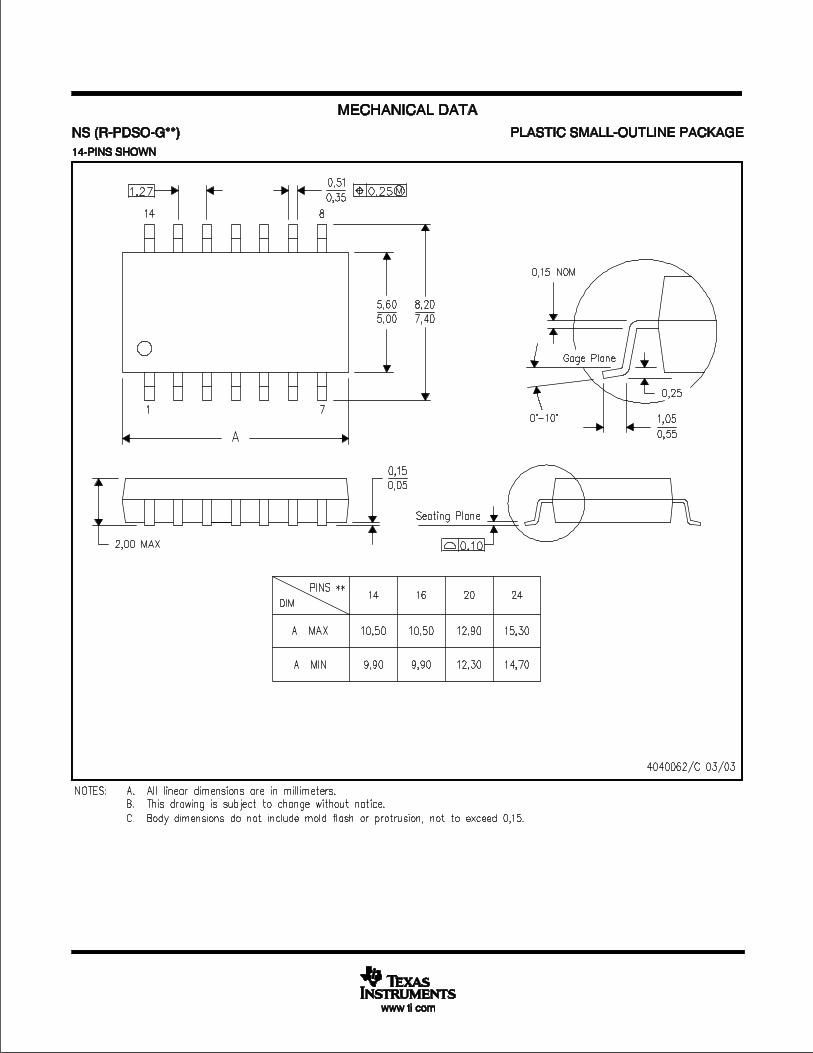
MECHANICAL DATA
MSSO002E – JANUARY 1995 – REVISED DECEMBER 2001
POST OFFICE BOX 655303 • DALLAS, TEXAS 75265
DB (R-PDSO-G**) PLASTIC SMALL-OUTLINE
4040065 /E 12/01
28 PINS SHOWN
Gage Plane
8,207,40
0,550,95
0,25
38
12,90
12,30
28
10,50
24
8,50
Seating Plane
9,907,90
30
10,50
9,90
0,38
5,605,00
15
0,22
14
A
28
1
2016
6,506,50
14
0,05 MIN
5,905,90
DIM
A MAX
A MIN
PINS **
2,00 MAX
6,90
7,50
0,65 M0,15
0°–8°
0,10
0,090,25
NOTES: A. All linear dimensions are in millimeters.B. This drawing is subject to change without notice.C. Body dimensions do not include mold flash or protrusion not to exceed 0,15.D. Falls within JEDEC MO-150