Embed Size (px)
Citation preview

www.elsevier.com/locate/photonics
Available online at www.sciencedirect.com
tals and Applications 6 (2008) 47–59
Photonics and Nanostructures – FundamenThe superprism effect in lithium niobate photonic crystals
for ultra-fast, ultra-compact electro-optical switching
J. Amet a, F.I. Baida a, G.W. Burr b, M.-P. Bernal a,*a Institut FEMTO-ST, Departement d’Optique P.M. Duffieux CNRS UMR 6174, Universite de Franche-Comte,
16 route de Gray, 25030 Besancon Cedex, Franceb IBM Almaden Research Center, 650 Harry Road, San Jose, CA 95120, USA
Received 15 June 2007; received in revised form 1 September 2007; accepted 6 September 2007
Available online 14 September 2007
Abstract
We numerically analyze ultra-refraction and slow-light in lithium niobate photonic crystals in order to investigate and then
optimize the efficiency of a tunable photonic crystal superprism. In contrast to a passive superprism 1-to-N demultiplexer, we
describe a tunable bandpass filter with only three output ports. The electro-optic effect in lithium niobate is used to achieve
tunability, with the filter bandwidth shifting in wavelength as the refractive index of the superprism is modified by an externally
applied electric field. Such a device could be used to realize a compact and fast wavelength multiplexer/demultiplexer for
telecommunications or optical interconnect applications. We calculate constant frequency dispersion contours (plane-wave
expansion) to identify initial configurations that show significant ultra-refraction, and verify the expected behavior of light
propagation inside the structure using 2D FDTD (finite difference time domain) simulations. We show that the voltage
requirements of such an electro-optically tunable superprism could potentially be relaxed by exploiting the enhancement of the
electro-optic effect recently discovered by our group [M. Roussey, M.-P. Bernal, N. Courjal, D. Van Labeke, F.I. Baida, Electro-
optic effect exaltation on lithium niobate photonic crystals due to slow photons. Appl. Phys. Lett. 89 (24) (2006) 241110],
which we believe to be due to the presence of slow-light in the nanostructure. We present a methodology that readily identifies
superprism design points showing both strong ultra-refraction as well as low group velocity. However, we find that this
improved voltage efficiency comes at the cost of reduced operating bandwidth and increased insertion losses due to proximity
to the band-edge.
# 2007 Elsevier B.V. All rights reserved.
PACS : 42.70.Qs; 42.82. �m; 78.20.Jq
Keywords: Photonic crystals; Electro-optic effect; Superprism effect; Lithium niobate
1. Introduction
Photonic crystals are periodic dielectric structures of
strong index contrast that make it possible to manipulate
and control light in devices as small as a few
* Corresponding author. Tel.: +33 3 81 66 64 10;
fax: +33 3 81 66 64 23.
E-mail address: [email protected] (M.P. Bernal).
1569-4410/$ – see front matter # 2007 Elsevier B.V. All rights reserved.
doi:10.1016/j.photonics.2007.09.002
wavelengths in size. Having become a widely studied
subject in the photonics community, many phenomena
such as perfect mirrors, photonic crystal waveguides,
and nano-cavities [2–4] have been discovered and
subsequently explored.
One intriguing property found in photonic crystals
is an unusual frequency dependence of the direction
of light propagation inside the photonic crystal [5].
This behavior was first reported in three-dimensional
(3D) photonic crystals fabricated in SiO2/Si and was

J. Amet et al. / Photonics and Nanostructures – Fundamentals and Applications 6 (2008) 47–5948
called the ‘‘superprism’’ phenomenon [6]. These
peculiar dispersion properties have motivated a
number of new micro-optical components such as
superlenses [7,8], negative refraction devices [7,9],
and wavelength multiplexing/demultiplexing devices
[10,11]. Such devices, the latter in particular, are of
great interest for optical processing and communica-
tions due to the possibility of separating the
wavelengths of an optical signal with a compact
device using ultra-refraction. While most of the first
devices proposed were passive, requiring the incident
angle or wavelength to be varied externally, more
recent works have introduced active superprism
devices. Here, the input angle and wavelength can
stay fixed, yet the propagation angle within the device
varies rapidly with small changes in the refractive
index of some portion of the photonic crystal
structure. Theoretical design studies for tunable
superprism devices have been published based on
both electro-optical [12,13] as well as liquid-crystal
[14] or nonlinear [15] materials.
In this work, we numerically investigate the
superprism effect for an index-tunable photonic
crystal located within a conventional lithium niobate
planar or stripe waveguide. First of all, we introduce
the concept of a tunable bandpass filter utilizing the
superprism effect. Then we briefly describe the
electro-optic effect in lithium niobate, and the
possibility for enhancement in the presence of slow
light. Constant frequency dispersion contours for a
design point offering strong ultra-refraction are
discussed, and the operation of the tunable bandpass
filter is investigated using 2D finite difference time
domain (FDTD) numerical simulations. In order to
further investigate and then exploit the enhancement
of the electro-optic effect by slow-light within the
photonic crystal nanostructure, we present a metho-
dology that readily identifies superprism design points
showing both strong ultra-refraction as well as low
group velocity. We find that this improved voltage
efficiency comes at the cost of reduced operating
bandwidth and increased insertion losses due to
proximity to the band-edge. We conclude that the
experimental characterization of both the wavelength
and index sensitivities of such a photonic crystal
superprism will be needed to provide improved
understanding of the electro-optic enhancement in
nanostructured lithium niobate. With such knowledge,
the tradeoff between voltage efficiency and bandwidth
can be quantified, leading to ultra-fast, ultra-compact
tunable bandpass filters in lithium niobate using the
superprism effect.
2. Active superprism devices as tunable
wavelength filters
Conventionally, the application most frequently
discussed with the superprism effect is a 1-to-N
demultiplexer [16,10,11], as shown schematically in
Fig. 1(a). Here, different wavelength-multiplexed
signals are split into a static distribution of distinct
output ports. When used in reverse, such a device
becomes a multiplexer. Theoretically, a photonic crystal
superprism should allow such a device to be quite
compact because of ultra-refraction (the angle at which
light is refracted changes rapidly with wavelength).
However, as numerous authors have shown, inherent
tradeoffs between the size and spatial-frequency content
of beams within a superprism device tend to impose a
limit on the number of possible output channels
[16,10,11,17,18]. Various alternative designs have been
introduced [17,18] which can increase the number of
output ports by combining negative refraction inside the
photonic crystal together with normal diffraction
outside the device. However, these approaches tend
to increase the overall device footprint.
In contrast, we propose a tunable photonic crystal
superprism device with only a small number of output
ports, to be used as a tunable wavelength filter. For
instance, the three-port voltage-controlled device
shown in Fig. 1(b) acts as a tunable bandpass filter.
A two-port device could serve as a tunable high-pass
filter. When the operating voltage is zero, the filter
selects out one narrow wavelength band into the center
output port, deflecting lower wavelengths into the upper
port and higher wavelengths into the lower port. But as
the operating voltage is changed, the particular
wavelength band dropped into the center port can be
tuned up or down. When operated in reverse, such a
device would implement a tunable wavelength combi-
ner. The functionality of the passive demultiplexer
shown in Fig. 1(a), as well as many other interesting
routing scenarios, could be implemented simply by
cascading a small number of such active superprism
wavelength filters.
Passive and active superprism devices share many
features and requirements. Large angle deflection with
small changes in wavelength are still necessary, and
both devices would need to offer low insertion losses
and minimal crosstalk between ports in order to be truly
interesting. Fortunately, as we show below, configura-
tions that would make good passive superprism devices
(large angle swing with wavelength change) also make
good active devices (large angle swing with change in
refractive index). However, since the number of desired

J. Amet et al. / Photonics and Nanostructures – Fundamentals and Applications 6 (2008) 47–59 49
Fig. 1. A prototypical application for a passive superprism device is a 1-to-N multiplexer/demultiplexer (a), in which ultra-refraction allows
different wavelengths to be statically routed to output ports within a compact footprint [16,10,11]. In contrast, we propose here a tunable bandpass-
filter (b), utilizing the superprism effect to steer input signals to one of three output ports. The wavelength dropped into the center port changes as the
operating voltage tunes the index of refraction of the photonic crystal device.
output paths is much smaller, the tradeoff imposed by
beam diffraction is much less crucial to the success of
the device. Instead, a critical aspect becomes the
practicality of imposing sufficiently large changes in
index of refraction, either through changes in voltage or
some other suitable control variable.
3. Electro-optic effect in lithium niobate and its
enhancement by nanostructure
The combination of excellent electro-optical,
acousto-optical, nonlinear optical and piezoelectric
properties together with chemical and mechanical
stability makes lithium niobate an ideal material for
integrated optoelectronics. In particular, lithium
niobate is widely used to fabricate high speed
modulators, waveguide devices, dispersion compen-
sators, waveform converters and parametric amplifiers
[19]. Furthermore, nano-structuring of this material,
while not trivial, is possible by focused ion beam
etching [20]. Recently, a square-lattice lithium niobate
photonic crystal was fabricated and experimentally
demonstrated as an electro-optically tunable filter
[21].
The electro-optic effect is the change in the refractive
index of a material induced by an applied external
J. Amet et al. / Photonics and Nanostructures – Fundamentals and Applications 6 (2008) 47–5950
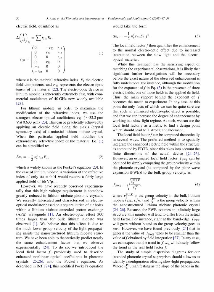
electric field, quantified as
D1
n2
� �i j
¼X
ri jk Ek;
ri jk ¼
0 �r22 r13
0 r22 r13
0 0 r33
0 r51 0
r51 0 0
�r22 0 0
0BBBBBB@
1CCCCCCA
(1)
where n is the material refractive index, Ek the electric
field components, and ri jk represents the electro-optic
tensor of the material [22]. The electro-optic device in
lithium niobate is inherently extremely fast, with com-
mercial modulators of 40 GHz now widely available
[23].
For lithium niobate, in order to maximize the
modification of the refractive index, we use the
strongest electro-optical coefficient: r33 (� 32.2 pm/
Vat 0.633 mm) [23]. This can be practically achieved by
applying an electric field along the z-axis (crystal
symmetry axis) of a uniaxial lithium niobate crystal.
When this particular applied field modifies the
extraordinary refractive index of the material, Eq. (1)
can be simplified to:
Dne ¼ �1
2n3
e r33 E3; (2)
which is widely known as the Pockel’s equation [23]. In
the case of lithium niobate, a variation of the refractive
index of only Dn ¼ 0:01 would require a fairly large
applied field of 66 V/mm.
However, we have recently observed experimen-
tally that this high voltage requirement is somehow
greatly reduced in lithium niobate photonic crystals.
We recently fabricated and characterized an electro-
optical modulator based on a square lattice of air holes
within a lithium niobate annealed proton exchange
(APE) waveguide [1]. An electro-optic effect 300
times larger than for bulk lithium niobate was
observed [1]. We believe that this effect is due to
the much lower group velocity of the light propagat-
ing inside the nanostructured lithium niobate struc-
ture. We have been able to theoretically predict nearly
the same enhancement factor that we observe
experimentally [24]. To do so, we introduced the
local field factor f , previously used to describe
enhanced nonlinear optical coefficients in photonic
crystals [25,26], into the Pockel’s equation. As
described in Ref. [24], this modified Pockel’s equation
would take the form
Dne ¼ �1
2n3
e r33 E3 f 3: (3)
The local field factor f then quantifies the enhancement
to the normal electro-optic effect due to increased
interaction between the slow light and the electro-
optical material.
While this treatment has the satisfying aspect of
matching the experimental observations, it is likely that
significant further investigations will be necessary
before the exact nature of the observed enhancement is
fully understood. For instance, although the motivation
for the exponent of f in Eq. (3) is the presence of three
electric fields, one of those fields is the applied dc field.
Thus, the main support behind the exponent of fbecomes the match to experiment. In any case, at this
point the only facts of which we can be quite sure are
that such an enhanced electro-optic effect is possible,
and that we can increase the degree of enhancement by
working in a slow-light regime. As such, we can use the
local field factor f as a metric to find a design point
which should lead to a strong enhancement.
The local field factor f can be computed theoretically
in several ways. The preferred method is to spatially
integrate the enhanced electric field within the structure
as computed by FDTD, since this takes into account the
finite dimensions of the actual device [24–26].
However, an estimated local field factor f PWE can be
obtained by simply comparing the group velocity within
the photonic crystal (as computed by the plane-wave
expansion (PWE)) to the bulk group velocity, as
f PWE ¼ffiffiffiffiffiffiffiffiffiffiffiffivBULK
g
vPCg
s; (4)
where vBULKg is the group velocity in the bulk lithium
niobate (e.g., c=ne) and vPCg is the group velocity within
the nanostructured lithium niobate photonic crystal
[24–26]. Because, the PWE assumes an infinitely large
structure, this number will tend to differ from the actual
field factor. For instance, right at the band-edge f PWE
will grow without bound as the group velocity goes to
zero. However, we have found previously [24] that in
general the value of f PWE tends to be smaller than the
value of f obtained by field integration [27]. In any case,
we can expect that the trend in f PWE will closely follow
the trend in the real field factor f .
The study of simple dispersion diagrams for our
intended photonic crystal superprism should allow us to
identify a configuration offering slow-light propagation.
Where vPCg , manifesting as the slope of the bands in the

J. Amet et al. / Photonics and Nanostructures – Fundamentals and Applications 6 (2008) 47–59 51
Fig. 2. Band diagram for an infinite photonic crystal in a triangular
lattice (a ¼ 525 nm, r ¼ 105 nm) of air holes (n ¼ 1) for a lithium
niobate substrate (ne ¼ 2:143) and TM polarization (electric field
parallel to the cylindrical axis of the holes). The red line represents the
normalized frequency of V ¼ 0:338 (equivalent to l ¼ 1:55 mm when
a ¼ 524 nm) corresponding to Fig. 3. Also shown is a schematic view
of the triangular lattice photonic crystal in both real and frequency
space.
dispersion diagram, tends to zero, then f PWE will
become very large and we can expect the real value of f
to be substantial as well. In such a case, based on our
previous experimental observations [1,24], we should
be able to greatly improve the efficiency with which the
electro-optic effect modifies the refractive index
through external field, enabling the realization of
ultra-compact electro-optic superprism devices.
Fig. 3. Constant frequency dispersion surfaces for a triangular lattice of circ
The incident angle is fixed at 23� from the GM direction and the incident wav
external applied electrical field is sufficient to reduce the refractive index of th
is at an angle of 0.6� from the GM direction. In contrast, when the sign of the
its zero-voltage value of 2.143 up to n ¼ 2:2 (b), the group velocity is at a
4. Electro-optically tunable superprism
Our overall goal is to find a set of parameters for an
electro-optic photonic crystal superprism device that is
efficiently tunable, yet which will also be feasible to
fabricate. Two different configurations are compared:
the first, based on the standard Pockel’s equation
(Eq. (2)), has been selected for good ultra-refraction
behavior but with no consideration of group velocity.
Thus, as will be shown, this first configuration requires a
high external voltage for significant angle swings. The
second configuration has been found with the additional
requirement of a high local field factor f PWE (low group
velocity), so that the external voltage needed for the
same beam steering can be significantly reduced. In this
work, we only take into account TM polarization (the
electric field vector parallel to the cylindrical axis of the
holes). This corresponds to a photonic crystal fabricated
on a X-cut crystal of lithium niobate in which a planar or
stripe waveguide has been created by in-diffusion of
titanium [28].
We choose to work with a triangular lattice of air
holes in order to achieve strong ultra-refraction, a
reasonable hole-size amenable to a realistic fabrication
process, and a structure with a low air-fraction in order
to maximize the effect of changes in substrate index.
The dispersion diagram of this 2D photonic crystal
obtained with the PWE method [29,30] is shown in
Fig. 2 for r=a ¼ 0:2, where a is the lattice periodicity
ular air holes in lithium niobate substrate (a ¼ 525 nm, r ¼ 105 nm).
elength is l ¼ 1:55 mm (V ¼ 0:338 for a ¼ 524 nm). In (a), when the
e lithium niobate to n ¼ 2:1, the power flow inside the photonic crystal
external electrical field is inverted to increase the refractive index from
n angle of �59�.

J. Amet et al. / Photonics and Nanostructures – Fundamentals and Applications 6 (2008) 47–5952
Fig. 4. Angle of the group velocity vector within a lithium niobate
triangular lattice photonic crystal as a function of both refractive index
ne and external electric field Ez, for the configuration described in
Fig. 3. The scaling from index change to electric field is performed
with the conventional Pockel’s equation, Eq. (2). An angle change of
60� occurs for a 4.67% change in index of refraction, requiring a
change in external field of 660 V/mm.
and r is the hole radius. Note that the cardinal directions
have been chosen here to correspond correctly to the
required crystal axes of the lithium niobate substrate. At
the normalized frequency V ¼ va=2pc ¼ a=l ¼ 0:338
marked by the red dashed line, the propagating Bloch
mode is located in the second lower band.
The constant frequency dispersion contours at this
normalized frequency (Fig. 3(a)) exhibit a hexagonal
shape that clearly present some interesting regions [31].
In particular, near the K point(s) of the Brillouin zone
the dispersion contour bends sharply with spatial
frequency. To couple into this spatial frequency inside
the photonic crystal, we can illuminate the GK interface
of the photonic crystal at an incident angle of 23� from
the GM direction. Conservation of the kz component
determines the wavevector kPC in the photonic crystal,
while the direction of the group velocity vector, vg, is
perpendicular to the tangent of the dispersion surface
[31]. The magnitude of the group velocity can be
obtained by using frequency contours at nearby
normalized frequencies to compute the gradient rkv
at this operating point ðkz; ky;VÞ. Although the use of
the PWE method and vectors lying on dispersion
contours implies an infinitely wide input beam, this
assumption is a reasonable first approximation given
that the stripe lithium niobate waveguides we typically
use are � 7 mm in width (approximately 10� larger
than l=ne).
The operation of previous superprism devices
depended on the fact that the dispersion contours of
constant frequency (in both the bulk and the photonic
crystal) change when either the refractive index or the
wavelength vary. But the tunable bandpass filter
described in Fig. 1 requires both of these effects. At
a constant wavelength, we want to be able to steer light
to a particular output port depending on the particular
index of refraction, as imposed by the control voltage.
However, for a given applied voltage, we also want
different wavelengths to steer to different ports. Here we
use constant frequency contours to check that both of
these effects are present with sufficiently large angle
changes.
Fig. 3 shows two constant frequency dispersion
curves for a constant input wavelength (normalized
frequency V ¼ 0:338, corresponding to l ¼ 1:55 mm if
a ¼ 525 nm). Using an incident angle of 23�, upon a
decrease in refractive index to n ¼ 2:1 due to the
application of a large external electric field (Fig. 3(a)),
the group velocity vector associated with power flow
inside the photonic crystal is at an angle of 0.6� (from
the GM direction). However, if the refractive index
increases to n ¼ 2:2, then the angle of the group
velocity vector is �59� (Fig. 3(b)). Fig. 4 shows the
continuous change in group velocity direction as the
index is varied from n ¼ 2:1 to 2.2. According to
Eq. (2), this index variation would require an applied
electric field of 660 V/mm, as shown on the upper
horizontal axis of Fig. 4. Thus, if no special precautions
are taken in choosing the design point, the angular
sensitivity is � 13� for a refractive index variation of
1%. This corresponds to � 13� for a change in applied
electric field of þ140 V/mm. This calculated index
sensitivity is approximately the same as that predicted
for PLZT devices [12,13].
Just as a passive superprism device is used as a
wavelength demultiplexer, the active superprism device
described in Fig. 1(b) also needs to be able to steer
beams solely on the basis of wavelength (at constant
index of refraction). In Fig. 5, constant frequency
contours are shown for two different normalized
frequencies (V ¼ 0:350 and 0.328), corresponding to
1.5 and 1.6 mm for an appropriate choice of a (525 nm).
With light incident at 23 �, the direction of the light
inside the photonic crystal is equal to �70� for
l ¼ 1:5 mm, and to 10� for l ¼ 1:6 mm (angles
measured from the GM direction). The sensitivity of
our device can be estimated to be � 0.8�/nm, roughly
the same order of magnitude as found in earlier work on
passive superprisms [32–34].
It would seem that the continuous angle deflection
shown in Fig. 4 would be incompatible with abrupt

J. Amet et al. / Photonics and Nanostructures – Fundamentals and Applications 6 (2008) 47–59 53
Fig. 5. Constant frequency dispersion surfaces for a triangular lattice of circular air holes in lithium niobate substrate with no applied voltage
(a ¼ 525 nm, r ¼ 105 nm, n ¼ 2:143). When the incident angle is fixed at 23� from the GMdirection, an incident wavelength of l ¼ 1:5 mm (a),
V ¼ 0:350 for a ¼ 525 nm) couples into a wavefront inside the photonic crystal with power flow at an angle of �70� from the GM direction. In
contrast, an incident wavelength of l ¼ 1:6 mm (b), V ¼ 0:328) corresponds to a group velocity at an angle of 10�.
switching of light from one output port into another.
However, we show with 2D finite difference time
domain (FDTD) simulations that we can in fact
implement the tunable bandpass filter described by
Fig. 1(b) with the same design point represented by
Figs. 3–5.
We perform FDTD simulations with a Gaussian
beam of 7-mm width incident on 25� 20 air holes
arranged in a triangular lattice photonic crystal
(r=a ¼ 0:2, a ¼ 524 nm). The GK interface is tilted
Fig. 6. Out-of-plane electric field amplitude as calculated by 2D FDTD for
substrate. The structure is rotated so that light with an initial spatial Gaussi
direction. As in Fig. 3, a ¼ 525 nm, r ¼ 105 nm, and the index of the lithiu
wavelength of l ¼ 1:49 mm, for which most of the power is refracted by a larg
the light is transmitted through the crystal with only a small refraction angle.
band, so that most of the light reflects from the photonic crystal.
by 23� with respect to the input beam. The 7-mm beam
width corresponds to the output mode of a stripe
waveguide fabricated by titanium diffusion into the top
surface of a lithium niobate substrate. Although these
are 2D simulations, in a real device light would be
confined vertically to a depth of 2–3 mm below the
substrate surface by the gradient index profile intro-
duced by titanium in-diffusion. Thus, as long as the
holes are deep enough to interact with this mode, these
2D simulations should still be quite descriptive of the
a triangular lattice of 25� 20 circular air holes in a lithium niobate
an profile of 7 mm width is incident at an angle of 23� from the GM
m niobate substrate is n ¼ 2:143. Part (a) corresponds to an incident
e (negative) angle. Part (b) corresponds to l ¼ 1:58 mm where most of
In Part (c), the incident wavelength of l ¼ 1:67 mm falls into the stop-
J. Amet et al. / Photonics and Nanostructures – Fundamentals and Applications 6 (2008) 47–5954
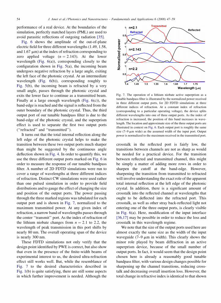
Fig. 7. The operation of a lithium niobate active superprism as a
tunable bandpass filter is illustrated by the normalized power received
in three different output ports, for 2D FDTD simulations at three
different indices of refraction. At a constant index of refraction
(corresponding to a particular operating voltage), the device splits
different wavelengths into one of three output ports. As the index of
refraction is increased, the position of this band increases in wave-
length. The location and approximate size of the three output ports are
illustrated in context on Fig. 6. Each output port is roughly the same
size (7–9 mm wide) as the assumed width of the input port. Output
power is normalized to the maximum received in the transmitted port.
performance of a real device. At the boundaries of the
simulation, perfectly matched layers (PML) are used to
avoid parasitic reflections of outgoing radiation [35].
Fig. 6 shows the amplitude of the out-of-plane
electric field for three different wavelengths (1.49, 1.58,
and 1.67 mm) at the index of refraction corresponding to
zero applied voltage (n ¼ 2:143). At the lower
wavelength (Fig. 6(a)), corresponding closely to the
configuration shown in Fig. 5(a), the incoming beam
undergoes negative refraction by a large angle, exiting
the left face of the photonic crystal. At an intermediate
wavelength (Fig. 6(b)), corresponding roughly to
Fig. 5(b), the incoming beam is refracted by a very
small angle, passes through the photonic crystal and
exits the lower face to continue as a transmitted beam.
Finally at a large enough wavelength (Fig. 6(c)), the
band-edge is reached and the signal is reflected from the
outer boundary of the photonic crystal. Thus, the third
output port of our tunable bandpass filter is due to the
band-edge of the photonic crystal, and the superprism
effect is used to separate the first two output ports
(‘‘refracted’’ and ‘‘transmitted’’).
It turns out that the total internal reflection along the
left edge of the photonic crystal helps to make the
transition between these two output ports much sharper
than might be suggested by the continuous angle
deflection shown in Fig. 4. In order to quantify this, we
use the three different output ports marked on Fig. 6 in
order to measure the response of our tunable bandpass
filter. A number of 2D FDTD simulations were run to
cover a range of wavelengths at three different indices
of refraction. Distinct CW simulations were used rather
than one pulsed simulation in order to provide field
distributions and to gauge the effect of changing the size
and position of the output ports. The power passing
through the three marked regions was tabulated for each
output port and is shown in Fig. 7, normalized to the
maximum transmitted power. At any given index of
refraction, a narrow band of wavelengths passes through
the center ‘‘transmit’’ port. As the index of refraction of
the lithium niobate changes from n ¼ 2:1 to 2.2, the
wavelength of peak transmission in this port shifts by
nearly 80 nm. The overall operating span of the device
is nearly 300 nm.
These FDTD simulations not only verify that the
design point identified by PWE is correct, but also show
that even in the presence of the finite-width beams of
experimental interest to us, the desired ultra-refraction
effect still works well. But, while the resemblance of
Fig. 7 to the desired characteristics described in
Fig. 1(b) is quite satisfying, there are still some aspects
in which further improvement is needed. Although the
crosstalk in the reflected port is fairly low, the
transitions between channels are not as sharp as would
be needed for a practical device. For the transition
between reflected and transmitted channel, this might
be simply a matter of adding more rows in order to
sharpen the cutoff at the band-edge. However,
sharpening the transition from transmitted to refracted
will involve understanding the exact role of the apparent
total internal reflection at the left edge of the photonic
crystal. In addition, there is a significant amount of
crosstalk into the reflected channel at wavelengths that
ought to be deflected into the refracted port. This
crosstalk, as well as other stray back-reflected light not
entering one of the three output ports, is clearly visible
in Fig. 6(a). Here, modification of the input interface
[36,17] may be possible in order to reduce the loss and
crosstalk in this wavelength regime.
We note that the size of the output ports used here are
almost exactly the same size as the width of the input
waveguide (7–9 mm in width). This clearly shows the
minor role played by beam diffraction in an active
superprism device, because of the small number of
output ports. In fact, it would seem that the design point
chosen here is already a reasonably good tunable
bandpass filter, with various design changes possible for
sharpening up the channel transitions, reducing cross-
talk and decreasing overall insertion loss. However, the
total change in refractive index is identical to that shown

J. Amet et al. / Photonics and Nanostructures – Fundamentals and Applications 6 (2008) 47–59 55
in Fig. 4. Thus, the standard Pockel’s equation would
predict that in order to implement the device shown in
Fig. 7, we would need to apply electric fields as large as
�330 V/mm across the device. In the remainder of the
paper, we try to find design points that might help
reduce this voltage swing by combining strong ultra-
refraction together with slow-light enhancement of the
electro-optic effect.
5. Electro-optically tunable superprism
enhanced by slow-light
Our objective now is to try to reduce operating
voltages by moving our tunable superprism design into
a regime where the electro-optic effect will be enhanced
by slow light propagation. So, we need to find a suitable
configuration in which both slow light and a strong
ultra-refraction effect are both present. This would
allow us to design a tunable superprism device that
would be both sub-millimeter in size and low-voltage.
To aid in our search for a suitable design point, we
perform multiple PWE computations across a range of
r=a, n, uin, and normalized frequency V, for both GK
Fig. 8. Group velocity direction uvg (a) and local field factor f PWE (b),
as calculated by the PWE algorithm and parameterized in color as a
function of the normalized frequency V and incident angle uin, for a
particular hole radius (r=a ¼ 0:2), index of refraction (n ¼ 2:143),
and lattice orientation (lattice terminated along GK). Design config-
urations offering no photonic crystal mode to couple into, or more than
one photonic crystal mode to couple into, are shown in gray and black,
respectively.
and GM lattice termination. For each of these many
design configurations, we compute both uvg and f PWE.
We are looking for design points where a small change
in index changes uvg by a large amount and the group
velocity is low (as quantified by a large f PWE). We can
compactly examine this set of results in the form of two-
dimensional design maps. Shown in Fig. 8 are the
calculated group velocity direction uvg (Fig. 8(a)) and
local field factor f PWE (Fig. 8(b)), parameterized in
color as a function of the normalized frequency V and
incident angle uin, for one particular hole radius
(r=a ¼ 0:2), index of refraction (n ¼ 2:143), and lattice
orientation (lattice terminated along GK). Just by
themselves, these maps are quite informative, since
rapid color changes on the first (Fig. 8(a)) identify
regions where the dispersion curves change curvature
rapidly (thus leading to strong ultra-refraction), while
the other (Fig. 8(b)) identifies band-edges where group
velocity falls abruptly (thus leading to large f PWE).
The smallest value of f PWE, corresponding to the
upper bound on group velocity within the photonic
crystal, might be expected to be slightly lower than the
index of refraction of bulk lithium niobate because a
small fraction (14.5%) of the device is air. From a
weighted sum of these two indices, we obtain a lower
bound on f PWE of 0.96. In practice, the lowest value of
f PWE we calculate is approximately 0.99. The field factor
values f PWE then increase to larger values near the band-
edges of the photonic crystal due to the presence of slow-
light. However, there are some parameter combinations
where no relevant superprism solution is possible
(marked on both Fig. 8(a) and (b) in gray), as well as
Fig. 9. Design metric for slow-light ultra-refraction with r=a ¼ 0:2
and GK lattice termination, defined as log ð1=2Þ ð f PWEjn1ðþ f PWEjn2 Þjuvg j
n2 � uvg jn1 jÞ, created by combining the pair of design
maps shown in Fig. 8 for n1 ¼ 2:143 together with a similar pair (not
shown) corresponding to n2 ¼ 2:160. The logarithm is used only to
help the linear colormap show both excellent (red) and moderately
good (yellow) design solutions. Six interesting design configurations
are identified with white arrows, with corresponding constant fre-
quency dispersion surfaces shown in Fig. 10(a–f).

J. Amet et al. / Photonics and Nanostructures – Fundamentals and Applications 6 (2008) 47–5956
regions where more than one relevant superprism
solution is possible. Since these design points would
lead to refraction of multiple beams within the photonic
crystal, we remove these from consideration as well
(regions colored black on both Fig. 8(a) and (b)).
By taking both the pair of design maps shown in
Fig. 8 for index of refraction n1, together with the pair
corresponding to a different index of refraction n2, we
can compute an overall slow-light superprism design
metric, defined as
log
�f PWEjn1 þ f PWEjn2
2juvgjn2 � uvg
jn1 j�: (5)
Fig. 10. Constant frequency dispersion surfaces for a triangular lattice of circ
interesting design configurations identified in Fig. 9; as well as to (g–i) thre
(not shown) for r=a ¼ 0:2 and GM lattice termination.
This design metric is shown parameterized in color in
Fig. 9, for n1 ¼ 2:143 and 2.160. This equation simply
quantifies the idea that we are looking for design
configurations where the group velocity stays low (high
f PWE) and the angle-change induced by refractive index
change is also large. The logarithm is used only to help
the linear colormap show both excellent (red) and
moderately good (green and yellow) design solutions.
Note that for the gray and black regions corresponding
to zero and more than one superprism solutions, respec-
tively, we have simply set the design metric to a very
low number (dark blue) so as to avoid such design
configurations.
ular air holes in lithium niobate substrate, corresponding to (a–f) the six
e additional design configurations from the similar design-metric map

J. Amet et al. / Photonics and Nanostructures – Fundamentals and Applications 6 (2008) 47–59 57
Fig. 11. Angle of the group velocity vector within a lithium niobate
triangular lattice photonic crystal as a function of both refractive index
ne and external electric field Ez, for r=a ¼ 0:2, uin ¼ 30:0�, V ¼ 0:32,
and GK termination (similar to Fig. 10(c)). Here the scaling from
index change to electric field is performed with the slow-light
enhanced Pockel’s equation, Eq. (3), with the local field factor taken
to be f ¼ 3. Considering the operation range from n = 2.13 to 2.165,
an angle change of � 105� occurs for a 1.63% change in index of
refraction, yet requires only a change in external field of 8 V/mm.
Insets show the out-of-plane electric field computed with 2D FDTD at
two different indices of refraction, for an input beam of 10 mm width.
The choice of n2 ¼ 2:160 is somewhat but not
completely arbitrary—a choice of n2 too close to n1 ¼ne will tend to weight f PWE more importantly than the
fairly small change in uvg . In contrast, an n2 value
widely different from n1 will tend to overvalue Duvg ,
since at least one of the two design conditions (n1 or n2)
will not be near the band-edge.
For this value of r=a ¼ 0:2 and termination along
GK, Fig. 9 shows a number of interesting candidates
where both strong ultra-refraction and low group
velocity can be found in the same design configuration.
We have picked out six such likely candidates (marked
with white arrows in Fig. 9) and show the corresponding
equifrequency contours with a representative super-
prism solution in parts (a–f) of Fig. 10. Fig. 10(g–i)
shows three similar configurations found on the map for
r=a ¼ 0:2 but when the incoming light is incident upon
a photonic crystal lattice terminated along GM (maps
not shown). Note that for these latter three solutions, the
conserved wavevector component is oriented at 90�
with respect to earlier such equifrequency/superprism
contours. Each superprism configuration is shown at an
input angle and normalized frequency which makes the
superprism behavior obvious at n ¼ 2:143. However,
one can realize the same functionality at a nearby r=a or
incident angle, by slightly changing the index of
refraction or the incident wavelength. Thus, even in the
presence of some fabrication error, we should still have
the opportunity to observe the efficiently tunable
superprism effect.
To quantify this efficient tunability, we pick one
particular configuration, near uin ¼ 30:5� and
V ¼ 0:320, corresponding to Fig. 10(c). Shown in
Fig. 11 is the group velocity angle as a function of
refractive index for this configuration, shown at uin ¼30:0� and V ¼ 0:320 for r=a ¼ 0:2 and GK termina-
tion. Note that because of the operation near the band-
edge, a swing of � 105� is realized for a refractive index
change of � 0.035, or 65� for each 1% index change.
This is already a 5-fold improvement in ultra-refraction
over our first design. Shown in the inset of Fig. 11 are
the out-of-plane electric field at two different index of
refraction values obtained by 2D FDTD, with a input
beam only slightly wider than used earlier (10 mm). The
field enhancement within the photonic crystal structure
is clear, and the anticipated beam-steering would be
clearly visible in a near-field measurement (although
less so in far-field).
Since this design configuration also has a larger field-
factor, we can expect the scaling between index of
refraction and applied electric field to follow the
enhanced version of the Pockel’s equation (Eq. (3))
rather than the standard equation for bulk material
(Eq. (2)). Given our still imperfect knowledge about the
nature of the enhancement, quantifying the potential
reduction in voltage requirements is somewhat tricky.
To do so, we have chosen to use a value of f ¼ 3. We
make this choice as a tradeoff, one which is more
conservative than the value of f ¼ 7 found in our earlier
experimental work on square-lattice photonic crystals
[1,24]. We rationalize this because in that work, the
light was propagating parallel to a Brillouin zone edge,
where group velocities are known to become extremely
low. However, this choice is slightly more aggressive
than the f PWE values calculated for this particular
design point (which range from f PWE = 1.6–2.0 within
the main tuning range). This follows the observed
relationship found in Ref. [24] that the f PWE as
calculated from group velocities is roughly 50% lower
than the corresponding field factor value f obtained by
integrating electric field within the structure (see also
[27]).
In any case, this choice of f ¼ 3 leads to a prediction
that an angle swing of 105� would require a change in
applied electric field of only 8 V/mm. For electrodes
spaced at 13 mm as in Ref. [1,24], this would require
104 V, just slightly larger than the voltage changes used
in that work. Comparing the angle-change per volt
J. Amet et al. / Photonics and Nanostructures – Fundamentals and Applications 6 (2008) 47–5958
between this configuration (Fig. 11) and our first (Fig. 4)
which did not exploit slow light, we find that designing
specifically for the slow-light enhancement of the
electro-optic effect might be able to produce a 145-fold
improvement in the efficiency of an appropriately
designed electro-optically tunable active superprism.
The inherent cost in this design point is that at these
kinds of locations within the dispersion diagram, the
electro-optic enhancement can only be applied over a
small bandwidth around the operating wavelength. This
is because high local field factors are only found right
near or at the band-edges. Visually, this is readily
apparent in Fig. 9 because the design points showing
strong ultra-refraction together with low group velocity
all lie on narrow rim around the band-gap. In addition,
the insets of Fig. 11 make it clear that the problems of
efficient coupling into and out of the photonic crystal
are only exacerbated by operation near the band-edge.
Thus, there will be a strong trade-off between the
efficiency of the tuning (a large angle-change per volt)
and the other desirable aspects of the active superprism
device (total angle-change, high operating bandwidth,
low crosstalk, and low insertion loss).
Even though the design point shown in Fig. 11 is not
necessarily more attractive than the one evaluated
earlier (Figs. 3–7), there is still a very good reason to
build and characterize it. Because the superprism effect
can be measured independently under both wavelength
and index change, the device shown in Fig. 11 would
provide an excellent opportunity to provide further
experimental data for understanding the electro-optic
enhancement in nanostructured lithium niobate photo-
nic crystals. For instance, one could directly compare
the sensitivity of the angle deflection with voltage
against the sensitivity with wavelength change at a
constant voltage. This helps bypass a number of
inherent experimental uncertainties that otherwise tend
to complicate such a measurement. The testing of
superprism devices designed to operate at various
degrees of proximity to the band-edge can help
complete our understanding of the enhanced electro-
optic effect. Then, we can better quantify the tradeoff
between increased efficiency and the loss of operating
bandwidth, allowing us to pick an optimal design point
that is close but not ‘‘too close’’ to the band-edge.
Thus, the next logical steps for future research are
to extend the procedure developed here to the case of
in-plane polarization, and then to fabricate a suitable
device using an annealed-proton exchanged (APE)
lithium niobate waveguide. An APE (rather than
diffused titanium) waveguide will help keep the
optical mode closer to the surface, providing better
overlap with cylindrical holes of finite depth (as
fabricated by milling with a focused ion beam). It may
also be useful to fabricate such a photonic crystal in a
deep trench etched into the substrate surface, in order
to force the mode to interact with the holes and to more
easily observe this interaction with a near-field optical
probe. With such a fabricated device, one can
experimentally verify the presence and magnitude
of this enhanced superprism effect, and then feed new
information obtained via experiment back into
subsequent designs.
6. Conclusions
An active photonic crystal superprism device using
the electro-optic effect in lithium niobate would be an
extremely attractive device for the future realization of
ultra-fast, ultra-compact optical components for opti-
cal processing and interconnect. In contrast to previous
passive multiplexer designs, we propose a novel active
superprism device which implements a three-port
tunable bandpass filter. We illustrate the operation of
this device over a reasonable bandwidth using 2D
FDTD numerical simulations. In order to improve the
voltage-tuning efficiency of the device, we introduce a
methodology for visualizing the design space repre-
sented by extensive plane-wave expansion results. This
procedure readily identifies designs that combine both
strong ultra-refraction and low group velocity. We
theoretically predict that the slow-light enhancement of
the electro-optic effect in lithium niobate could
potentially increase the angle-change per volt by a
factor of 145 over designs that rely on ultra-refraction
alone. However, we observe that operation too close to
the band-edge sacrifices many of the other desirable
aspects of the active superprism device. Experimental
characterization of such near-band-edge superprism
devices will be a critical step towards better quanti-
tative understanding of this slow-light enhancement in
lithium niobate. In turn, this will then enable
quantitative assessment of the tradeoff between voltage
efficiency and operating bandwidth, leading to effi-
ciently tunable and high-performance active super-
prism devices.
Acknowledgments
The authors want to thank INTERREG III
(‘‘CRISLAR’’) for financial support. GWB would
like to thank the CNRS and IBM management for
making his extended visit to FEMTO-ST in Besancon
possible.

J. Amet et al. / Photonics and Nanostructures – Fundamentals and Applications 6 (2008) 47–59 59
References
[1] M. Roussey, M.-P. Bernal, N. Courjal, D. Van Labeke, F.I. Baida,
Electro-optic effect exaltation on lithium niobate photonic crys-
tals due to slow photons, Appl. Phys. Lett. 89 (24) (2006)
241110.
[2] J.D. Joannopoulos, R.D. Meade, J.N. Winn, Photonic Crystals:
Molding the Flow of Light, Princeton University Press, Prince-
ton, NJ, 1995.
[3] J.D. Joannopoulos, P.R. Villeneuve, S.H. Fan, Photonic crystals:
Putting a new twist on light, Nature 386 (6621) (1997) 143–149.
[4] O. Painter, R.K. Lee, A. Scherer, A. Yariv, J.D. O’Brien, P.D.
Dapkus, I. Kim, Two-dimensional photonic band-gap defect
mode laser, Science 284 (5421) (1999) 1819–1821.
[5] S.Y. Lin, V.M. Hietala, L. Wang, E.D. Jones, Highly dispersive
photonic band-gap prism, Opt. Lett. 21 (21) (1996) 1771–1773.
[6] H. Kosaka, T. Kawashima, A. Tomita, M. Notomi, T. Tamamura,
T. Sato, S. Kawakami, Superprism phenomena in photonic
crystals, Phys. Rev. B 58 (16) (1998) R10096–R10099.
[7] B. Gralak, S. Enoch, G. Tayeb, Anomalous refractive properties
of photonic crystals, J. Opt. Soc. Am. A17 (6) (2000)
1012–1020.
[8] X. Hu, C.T. Chan, Photonic crystals with silver nanowires as a
near-infrared superlens, Appl. Phys. Lett. 85 (9) (2004) 1520–
1522.
[9] R.A. Shelby, D.R. Smith, S. Schultz, Experimental verification
of a negative index of refraction, Science 292 (5514) (2001)
77–79.
[10] A. Lupu, E. Cassan, S. Laval, L. El Melhaoui, P. Lyan,
J.M. Fedeli, Experimental evidence for superprism phenomena
in soi photonic crystals, Opt. Exp. 12 (23) (2004) 5690–
5696.
[11] T. Matsumoto, S. Fujita, T. Baba, Wavelength demultiplexer
consisting of photonic crystal superprism and superlens, Opt.
Exp. 13 (26) (2005) 10768–10776.
[12] D. Scrymgeour, N. Malkova, V. Sungwon Kim, Gopalan, Electro
optic control of the superprism effect in photonic crystals, Appl.
Phys. Lett. 82 (19) (2003) 3176–3178.
[13] S. Xiong, H. Fukshima, Analysis of light propagation in
index tunable photonic crystals, J. Appl. Phys. 94 (2) (2003)
1286–1288.
[14] G. Alagappan, X.W. Sun, M.B. Yu, P. Shum, D. den Engelsen,
Tunable dispersion properties of liquid crystal infiltrated into a
two-dimensional photonic crystal, IEEE J. Quant. Electr. 42 (3/
4) (2006) 404–409.
[15] N.C. Panoiu, M. Bahl, R.M. Osgood, Optically tunable super-
prism effect in nonlinear photonic crystals, Opt. Lett. 28 (24)
(2003) 2503–2505.
[16] T. Baba, T. Matsumoto, Resolution of photonic crystal super-
prism, Appl. Phys. Lett. 81 (13) (2002) 2325–2327.
[17] J. Witzens, T. Baehr-Jones, A. Scherer, Hybrid superprism with
low insertion losses and suppressed cross-talk, Phys. Rev. E 71
(2) (2005) 026604.
[18] B. Momeni, A. Adibi, Optimization of photonic crystal demul-
tiplexers based on the superprism effect, Appl. Phys. B 77 (6–7)
(2003) 555–560.
[19] L. Arizmendi, Photonic applications of lithium niobate crystals,
Phys. Stat. Sol. A 201 (2) (2004) 253–283.
[20] F. Lacour, N. Courjal, M.P. Bernal, A. Sabac, C. Bainier, M.
Spajer, Nanostructuring lithium niobate substrates by focused
ion beam milling, Opt. Mater. 27 (8) (2005) 1421–1425.
[21] M. Roussey, M.P. Bernal, N. Courjal, F.I. Baida, Experimental
and theoretical characterization of a lithium niobate photonic
crystal, Appl. Phys. Lett. 87 (24) (2005) 241101.
[22] R.S. Weis, T.K. Gaylord, Lithium niobate: summary of physical
properties and crystal structure, Appl. Phys. A 37 (1985)
191–203.
[23] R.W. Boyd, Nonlinear Optics, Academic Press, 2003.
[24] M. Roussey, F.I. Baida, M.-P. Bernal, Experimental and theore-
tical observation of the slow light effect on a tunable photonic
crystal, J. Opt. Soc. Am. B 24 (6) (2007) 1416–1422.
[25] R. Frey, P. Delaye, G. Roosen, Non–linearities optiques du
troisieme ordre dans les cristaux photoniques, in: H. Rigneault,
J.-M. Lourtioz, C. Delalande, A. Levenson (Eds.), La nanopho-
tonique, Collection Technique et Scientifique des Telecommu-
nications, GET et Lavoisier, Paris, 2005, pp. 207–222.
[26] P. Delaye, M. Astic, R. Frey, G. Roosen, Transfer–matrix
modeling of four-wave mixing at the band edge of a one-
dimensional photonic crystal, J. Opt. Soc. Am. B 22 (11)
(2005) 2494–2504.
[27] Note that we have identified two minor errors in Ref. [24] which
pertain to the comparison between local field factor f obtained
from integration of electric field and the approximate local field
factor f PWE calculated from the group velocity. Due to a minor
typographical error, the y-label of Fig. 5 in that paper indicates
group velocities that are 1000 � too small. As a result, the value
of f PWE� 94 given in the text below this figure is too large by
the square root of 1000. The actual value of f PWE� 2:97 is thus
significantly smaller than the value of f calculated from FDTD
(Fig. 6 of Ref. [24] gives f � 4:8, and Fig. 7b shows f values as
large as 7).
[28] M.M. Abouelleil, F.J. Leonberger, Wave-guides in lithium-nio-
bate, J. Am. Ceram. Soc. 72 (8) (1989) 1311–1321.
[29] S.P. Guo, S. Albin, Simple plane wave implementation for
photonic crystal calculations, Opt. Exp. 11 (2) (2003) 167–175.
[30] BandSolve 3.0, RSoft Design Group, 2006.
[31] M. Notomi, Theory of light propagation in strongly modulated
photonic crystals: refraction like behavior in the vicinity of the
photonic band gap, Phys. Rev. B 62 (16) (2000) 10696–10705.
[32] H. Kosaka, T. Kawashima, A. Tomita, M. Notomi, T. Tamamura,
T. Sato, S. Kawakami, Photonic crystals for micro lightwave
circuits using wavelength-dependent angular beam steering,
Appl. Phys. Lett. 74 (10) (1999) 1370–1372.
[33] L.J. Wu, M. Mazilu, T. Karle, T.F. Krauss, Superprism phenom-
ena in planar photonic crystals, IEEE J. Quant. Electr. 38 (7)
(2002) 915–918.
[34] J.J. Baumberg, N.M.B. Perney, M.C. Netti, M.D.C. Charlton, M.
Zoorob, G.J. Parker, Visible-wavelength super-refraction in
photonic crystal superprisms, Appl. Phys. Lett. 85 (3) (2004)
354–356.
[35] A. Taflove, S.C. Hagness, Computational Electrodynamics: The
Finite-difference Time-domain Method, 3rd ed., Artech House,
Boston, 2005.
[36] T. Baba, T. Matsumoto, M. Echizen, Finite difference time
domain study of high efficiency photonic crystal superprisms,
Opt. Exp. 12 (19) (2004) 4608–4613.


![arXiv:1902.08969v1 [physics.app-ph] 24 Feb 2019cwang/publications/Low-loss...Integrated lithium niobate (LN) photonic circuits have recently emerged as a promising candidate for advanced](https://img.pdfslide.net/doc/110x75/611505d55fbd9378f64daaa2/arxiv190208969v1-24-feb-2019-cwangpublicationslow-loss-integrated-lithium.jpg)