Embed Size (px)
Citation preview

Thermal boundary conductance accumulation and interfacial phonon1
transmission: measurements and theory2
Ramez Cheaito,1, ∗ John T. Gaskins,1, ∗ Matthew E. Caplan,1 Brian F. Donovan,13
Brian M. Foley,1 Ashutosh Giri,1 John C. Duda,1, 2 Chester J. Szwejkowski,1 Costel4
Constantin,3 Harlan J. Brown-Shaklee,4 Jon F. Ihlefeld,4 and Patrick E. Hopkins1, †5
1Department of Mechanical and Aerospace Engineering,6
University of Virginia, Charlottesville, Virginia 22904, USA7
2Current address: Seagate Technology, Bloomington, MN 55435, USA8
3Department of Physics and Astronomy,9
James Madison University, Harrisonburg, VA 22807, USA10
4Electronic, Optical, and Nanomaterials Department,11
Sandia National Laboratories, Albuquerque, NM 87185, USA12
1

Abstract13
The advances in phonon spectroscopy in homogeneous solids have unveiled extremely useful physics14
regarding the contribution of phonon energies and mean free paths to the thermal transport in solids. How-15
ever, as material systems decrease to length scales less than the phonon mean free paths, thermal transport16
can become much more impacted by scattering and transmission across interfaces between two materials17
than the intrinsic relaxation in the homogeneous solid. To elucidate the fundamental interactions driv-18
ing this thermally-limiting interfacial phonon scattering process, we analytically derive and experimentally19
measure a thermal boundary conductance accumulation function. We develop a semi-classical theory to20
calculate the thermal boundary conductance accumulation function across interfaces using the diffuse mis-21
match model (DMM), and validate this derivation by measuring the interface conductance between nine22
different metals on native oxide/silicon substrates and five different metals on sapphire substrates. Mea-23
surements were performed at room temperature using time-domain thermoreflectance and represent the24
first-reported values for interface conductance across several metal/native oxide/silicon and metal/sapphire25
interfaces. The various metal films provide a variable bandwidth of phonons incident on the metal/substrate26
interface. This method of varying phonons cutoff frequency in the film while keeping the same substrate27
allows us to mimic the accumulation of thermal boundary conductance and thus provides a direct method to28
experimentally validate our theory. We show that the accumulation function can be written as the product29
of an average interfacial phonon transmission function and the accumulation of the temperature derivative30
of the phonon flux incident on the interface; this provides the framework to extract an average, spectrally31
dependent phonon transmissivity from a series of thermal boundary conductance measurements. Based on32
the assumptions made in this work and the measurement results on different metals on native oxide/silicon33
and sapphire substrates, we demonstrate that thermal transport across solid interfaces may not necessarily34
be dictated by phonon mismatch of materials and interfacial transmission, but is rather directly correlated35
to the temperature derivative of phonon flux incident on the interface.36
2

I. INTRODUCTION37
Solid-solid interfaces can dominate the thermal processes of devices and material systems when38
the interface spacing becomes less than the carrier mean free path. This has pronounced effects39
on thermal transport in nanosystems,1–3 as the rate of energy transmission across the interface40
between two solids is often less than the intrinsic rate of conduction in the solids. In fact, even41
the near-interface regions in a solid can lead to additional thermal resistance due to growth bi-42
products, atomic imperfections, chemical impurities, and other “non-idealities”.4 Although only43
a few studies have presented experimental measurements of the thermal boundary conductance44
across atomically smooth, chemically abrupt interfaces,5–7 even these works have shown that heat45
transport across these seemingly “perfect” interfaces can still generate a significant source of ther-46
mal resistance.47
Even with this thermal boundary conductance (or Kapitza conductance),8 hK, being immensely48
important to nanoscale thermal engineering of solids, a void exists in the current knowledge of49
how phonons interact at interfaces and spectrally contribute to hK. For example, measurements50
of thermal boundary conductance are typically compared to semi-classical models, such as the51
acoustic or diffuse mismatch models (AMM or DMM, respectively)9–11 to analyze how phonons52
are contributing to interfacial transport. However, due to the many assumptions inherent in these53
models, agreement between the model predictions and experimental data can often be argued as54
coincidence. This being said, several previous works, including our own, have developed refine-55
ments to the AMM and DMM to garner further insight into how phonon energies are transmitted56
across solid interfaces.12–28 Limitations imposed by the fundamental kinetic theory assumptions57
in which the AMM and DMM are rooted can still raise questions when simply comparing to58
experimental data.29 More rigorous classical molecular dynamics simulations have addressed sev-59
eral unanswered questions regarding phonon scattering and subsequent energy transfer across60
interfaces,30–49 however, these simulations can not account for quantum mechanical phonon pop-61
ulations below a material’s Debye temperature. As a result, the current understanding of how62
phonons couple and transmit energy across interfaces at moderate temperatures is limited by the63
mismatch theories or their variants.64
Due to these theoretical limitations, knowledge of the physics driving phonon thermal bound-65
ary conductance across solid interfaces has lagged considerably compared to the comprehension66
of phonon scattering processes in homogeneous media. Recent theoretical,50,51 computational52–5567
3
and experimental56–61 works have established the basis of an “accumulation function” for thermal68
conductivity in homogeneous solids, which has resulted in substantial advances in understanding69
how phonons scatter and transport energy in solids. This accumulation function provides a direct70
relationship between carrier mean free path and thermal energy transferred by a solid. The ability71
to define the accumulation function gives direct insight into how phonons couple energy to other72
carriers in a solid.73
Clearly, a “thermal boundary conductance accumulation function” would substantially ad-74
vance the field of phonon transport across interfaces, in nanosystems, and through composite75
media. Although this accumulation function can be easily calculated from the semi-classical mis-76
match theories, as shown below, an experimental measurement of this accumulation function will77
provide direct insight into phonon transmission across interfaces. Furthermore, an experimental78
measurement of this thermal boundary conductance accumulation would provide direct validation79
of the fundamental assumptions in theories for hK while providing a measure of how phonons are80
spectrally transmitting across solid interfaces.81
In this work, we report on a series of theoretical advancements and experimental measurements82
that provide evidence into how phonons transmit energy across solid interfaces at room temper-83
ature. In doing so, we directly assess the validity of the assumptions of phonon transmission84
calculations in the DMM. First, we analytically define the thermal boundary conductance accu-85
mulation function, and derive this accumulation function assuming diffusive scattering, one of the86
fundamental assumptions of the DMM. To validate this theory, we measure the thermal boundary87
conductance across interfaces of nine different metal films and silicon substrates with a native88
oxide layer. Our experiments show that for native oxide/silicon interfaces, the assumptions of89
the DMM are acceptable for describing interfacial phonon transmission. Additionally, we further90
support this assertion through a similar series of measurements on five different metal/sapphire91
interfaces.92
This work provides experimental measurements that give insight into the spectral nature93
of phonon transport across interfaces. Several previous works have computationally31,62 and94
experimentally63–65 shown that hK across solid/solid interfaces increases with an increase in95
phonon spectral overlap. However, this does not differentiate between the changing phonon96
energy flux and transmission probability as the phonon spectra is modified. In this current work,97
our experimental approach is to keep the substrate constant while changing the metal film de-98
posited on the substrate surface.99
4
We show that with a carefully designed experimental approach, a series of metal/substrate100
interfaces with different metals can be used as a measure of the spectral accumulation of phonon101
transmission into the substrate and accumulation of phonon thermal boundary conductance. Fur-102
thermore, the data we report provides benchmark values for various transition metal/native ox-103
ide/silicon thermal boundary conductances that currently do not exist in the literature. Our choice104
of various transition metals ensures that the metal/native oxide/silicon interface is well bonded so105
our results are not affected by weak interfacial adhesion.66–68 In doing so, we also report on the106
effects of a Ti adhesion layer between Au and native oxide/Si substrates and show that Ti layers107
as thin as 2 nm still exhibit thermal boundary conductances that are more in line with a “thick”108
Ti/Si interface. As a final result of our work, we show that regardless of the metal transducer, we109
are able to consistently measure the thermal conductivity of a single crystalline silicon substrate110
in agreement with bulk literature values within the experimental uncertainty.69–71 This further vali-111
dates time-domain thermoreflectance (TDTR) as an effective measurement tool for measuring the112
thermal conductivity of bulk materials.113
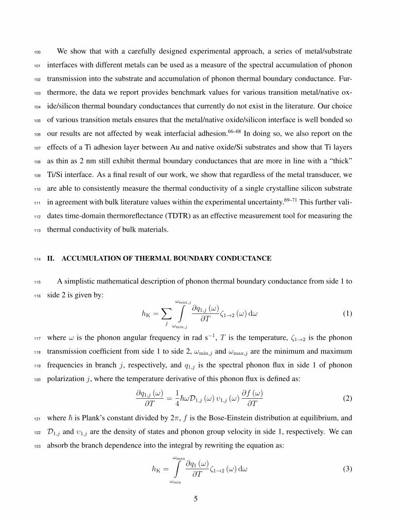
II. ACCUMULATION OF THERMAL BOUNDARY CONDUCTANCE114
A simplistic mathematical description of phonon thermal boundary conductance from side 1 to115
side 2 is given by:116
hK =∑j
ωmax,j∫ωmin,j
∂q1,j (ω)
∂Tζ1→2 (ω) dω (1)
where ω is the phonon angular frequency in rad s−1, T is the temperature, ζ1→2 is the phonon117
transmission coefficient from side 1 to side 2, ωmin,j and ωmax,j are the minimum and maximum118
frequencies in branch j, respectively, and q1,j is the spectral phonon flux in side 1 of phonon119
polarization j, where the temperature derivative of this phonon flux is defined as:120
∂q1,j (ω)
∂T=
1
4~ωD1,j (ω) υ1,j (ω)
∂f (ω)
∂T(2)
where ~ is Plank’s constant divided by 2π, f is the Bose-Einstein distribution at equilibrium, and121
D1,j and υ1,j are the density of states and phonon group velocity in side 1, respectively. We can122
absorb the branch dependence into the integral by rewriting the equation as:123
hK =
ωmax∫ωmin
∂q1 (ω)
∂Tζ1→2 (ω) dω (3)
5

where ωmax = max(ωmax,j), ωmin = min(ωmin,j) = 0 and ∂q1 (ω) /∂T is given by:124
∂q1 (ω)
∂T=∑j
∂q1,j (ω)
∂Twith
∂q1,j (ω)
∂T|ω>ωmax,jω<ωmin,j
= 0 (4)
Equation 3 expresses hK as a product of two functions. In parallel to previous theoretical works125
on thermal conductivity accumulation,50,51 we can now define a thermal boundary conductance126
accumulation, αK, as:127
αK,1→2 (ωα) =1
hK
ωα∫0
∂q1 (ω)
∂Tζ1→2 (ω) dω =
ωα∫0
hK (ω) dω (5)
which represents the fraction of the total thermal boundary conductance due to carriers in the metal128
(side 1) with phonon frequencies less than ωα transmitting energy to side 2. The equation on the far129
right of Eq. 5 recasts the integrand into a spectral thermal boundary conductance, hK. Ultimately,130
this accumulation function is dictated by the product of ∂q1/∂T and ζ1→2, both of which are131
dependent on frequency and therefore difficult to explicitly separate from this integral to compare132
with experimental data. However, we can separate these quantities using the Generalized Mean133
Value Theorem for definite integrals72 which states that there exists a frequency x ∈ [0, ωα] such134
that:135
αK,1→2 (ωα) =
(1
hK
)ζ1→2 (x (ωα))
ωα∫0
∂q1 (ω)
∂Tdω (6)
where ζ1→2 (x (ωα)) is the average of interfacial transmission from side 1 to side 2 over the fre-136
quency interval [0, ωα] weighted by ∂q1/∂T . Since ωα is the independent variable in our formula-137
tion, and x is a function of ωα we can write ζ1→2 solely as a function of ωα so that Eq. 6 becomes138
αK,1→2 (ωα) = (1/hK)QT (ωα) ζ1→2 (ωα) (7)
where QT (ωα) =∫ ωα0
∂q1/∂T dω is the un-normalized accumulation of ∂q1/∂T . We note that139
this approach provides the separation of flux and average transmission (which is related to the fun-140
damental mechanisms of phonon scattering at interfaces) in the formulation of thermal boundary141
conductance. We show example calculations of Eq. 5 in Fig. 1 for Al/Si and Au/Si interfaces using142143
DMM assumptions. This assumption of diffusive phonon scattering directly impacts calculations144
of the phonon transmissivity but not the calculations of the metal phonon flux. These assumptions145
and our specific procedure for the DMM are outlined in detail in our previous works, and are not146
repeated here.74,75 For these calculations, we ignore the contribution from optical modes and as-147
sume a 4th order polynomial fit to the one-dimensional phonon dispersion in the Γ→ X direction148
6

0 1 0 2 0 3 0 4 0 5 0 6 0 7 00
5 0
1 0 0
1 5 0
2 0 0
2 5 0
0 1 0 2 0 3 0 0 . 00 . 20 . 40 . 60 . 81 . 0
0 1 0 2 0 3 0 4 0 5 0 6 0 0 . 00 . 20 . 40 . 60 . 81 . 0
�q T
�q T( a )
( b ) A u / S i
( c ) A l / S iA u / S i
�K , 1 - 2
Accum
ulated
therm
al bou
ndary
cond
uctanc
e (MW
m-2 K-1 )
P h o n o n f r e q u e n c y ( T r a d s - 1 )
A l / S i�K , 1 - 2
FIG. 1. (a) Un-normalized accumulation of thermal boundary conductance for Al/Si and Au/Si interfaces
calculated with Eq. 5 without normalizing by hK. The features in curves are related to the cutoff frequencies
of the phonon branches. (b) and (c) Normalized accumulation of thermal boundary conductance (Eq. 5,
αK,1→2) and normalized accumulation of the temperature derivative of the phonon flux (αqT ) plotted as a
function of ωα for Au/Si and Al/Si, respectively. The various modeling calculations shown in these plots and
the MATLAB code used to generate these accumulation models are given in the supplementary materials.73
in Au (Ref. 76), Al (Ref. 77), and Si (Ref. 78), and an isotropic Brillouin zone, which is an ac-149
ceptable approximation for cubic structures.79 Finally, we assume two-phonon elastic scattering150
as the mechanism for phonon transmission across interfaces,20,21 and therefore we only conduct151
these calculations up to the maximum phonon frequencies in the metal which corresponds to the152
cutoff frequency of the longitudinal acoustic branch (e.g., frequencies above ∼30 Trad s−1 in Au153
are assumed to not contribute to hK). The dispersion curves used for this calculation are shown154
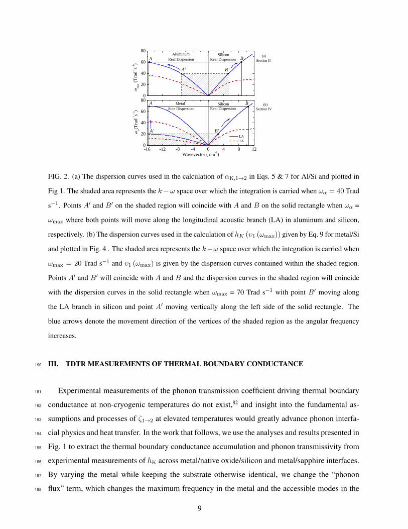
in Fig. 2(a) for aluminum on silicon denoted by ”Real Dispersion”. The shaded area in the figure155
represents the k − ω space over which the integration is carried when ωα = 40 Trad s−1, where k156
is the wavevector. In this case, the integration is carried over a subset of the Brillouin zone in the157
metal. Points A′ and B′ on the shaded region will coincide with A and B on the solid rectangle158
when ωα = ωmax. Note that the integration limits correspond to the angular frequency vector de-159
7
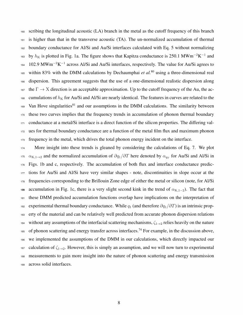
scribing the longitudinal acoustic (LA) branch in the metal as the cutoff frequency of this branch160
is higher than that in the transverse acoustic (TA). The un-normalized accumulation of thermal161
boundary conductance for Al/Si and Au/Si interfaces calculated with Eq. 5 without normalizing162
by hK is plotted in Fig. 1a. The figure shows that Kapitza conductance is 250.1 MWm−2K−1 and163
102.9 MWm−2K−1 across Al/Si and Au/Si interfaces, respectively. The value for Au/Si agrees to164
within 83% with the DMM calculations by Dechaumphai et al.80 using a three-dimensional real165
dispersion. This agreement suggests that the use of a one-dimensional realistic dispersion along166
the Γ→ X direction is an acceptable approximation. Up to the cutoff frequency of the Au, the ac-167
cumulations of hK for Au/Si and Al/Si are nearly identical. The features in curves are related to the168
Van Hove singularities81 and our assumptions in the DMM calculations. The similarity between169
these two curves implies that the frequency trends in accumulation of phonon thermal boundary170
conductance at a metal/Si interface is a direct function of the silicon properties. The differing val-171
ues for thermal boundary conductance are a function of the metal film flux and maximum phonon172
frequency in the metal, which drives the total phonon energy incident on the interface.173
More insight into these trends is gleaned by considering the calculations of Eq. 7. We plot174
αK,1→2 and the normalized accumulation of ∂q1/∂T here denoted by αqT for Au/Si and Al/Si in175
Figs. 1b and c, respectively. The accumulation of both flux and interface conductance predic-176
tions for Au/Si and Al/Si have very similar shapes - note, discontinuities in slope occur at the177
frequencies corresponding to the Brillouin Zone edge of either the metal or silicon (note, for Al/Si178
accumulation in Fig. 1c, there is a very slight second kink in the trend of αK,1−2). The fact that179180
these DMM predicted accumulation functions overlap have implications on the interpretation of181
experimental thermal boundary conductance. While q1 (and therefore ∂q1/∂T ) is an intrinsic prop-182
erty of the material and can be relatively well predicted from accurate phonon dispersion relations183
without any assumptions of the interfacial scattering mechanisms, ζ1→2 relies heavily on the nature184
of phonon scattering and energy transfer across interfaces.74 For example, in the discussion above,185
we implemented the assumptions of the DMM in our calculations, which directly impacted our186
calculation of ζ1→2. However, this is simply an assumption, and we will now turn to experimental187
measurements to gain more insight into the nature of phonon scattering and energy transmission188
across solid interfaces.189
8
02 04 06 08 0
- 1 6 - 1 2 - 8 - 4 0 4 8 1 202 04 06 08 0
� max (T
rad-1 s-1 ) R e a l D i s p e r s i o n
B 'BA
A '
A l u m i n u m S i l i c o nR e a l D i s p e r s i o n S e c t i o n I I
S e c t i o n I V( b )B
B '
AS i n e D i s p e r s i o n
M e t a lR e a l D i s p e r s i o n
S i l i c o n
� �(Tr
ad-1 s-1 )
W a v e v e c t o r ( n m - 1 )
L A T A
A '
( a )
FIG. 2. (a) The dispersion curves used in the calculation of αK,1→2 in Eqs. 5 & 7 for Al/Si and plotted in
Fig 1. The shaded area represents the k−ω space over which the integration is carried when ωα = 40 Trad
s−1. Points A′ and B′ on the shaded region will coincide with A and B on the solid rectangle when ωα =
ωmax where both points will move along the longitudinal acoustic branch (LA) in aluminum and silicon,
respectively. (b) The dispersion curves used in the calculation of hK (υ1 (ωmax)) given by Eq. 9 for metal/Si
and plotted in Fig. 4 . The shaded area represents the k−ω space over which the integration is carried when
ωmax = 20 Trad s−1 and υ1 (ωmax) is given by the dispersion curves contained within the shaded region.
Points A′ and B′ will coincide with A and B and the dispersion curves in the shaded region will coincide
with the dispersion curves in the solid rectangle when ωmax = 70 Trad s−1 with point B′ moving along
the LA branch in silicon and point A′ moving vertically along the left side of the solid rectangle. The
blue arrows denote the movement direction of the vertices of the shaded region as the angular frequency
increases.
III. TDTR MEASUREMENTS OF THERMAL BOUNDARY CONDUCTANCE190
Experimental measurements of the phonon transmission coefficient driving thermal boundary191
conductance at non-cryogenic temperatures do not exist,82 and insight into the fundamental as-192
sumptions and processes of ζ1→2 at elevated temperatures would greatly advance phonon interfa-193
cial physics and heat transfer. In the work that follows, we use the analyses and results presented in194
Fig. 1 to extract the thermal boundary conductance accumulation and phonon transmissivity from195
experimental measurements of hK across metal/native oxide/silicon and metal/sapphire interfaces.196
By varying the metal while keeping the substrate otherwise identical, we change the “phonon197
flux” term, which changes the maximum frequency in the metal and the accessible modes in the198
9
substrate that couple to the metal phonons. With relation to Fig. 1, by changing the metal film,199
we incrementally increase the phonon frequency on the accumulation curve (i.e., the metal film200
systematically changes the maximum value of ωα in Eq. 5). This approach yields direct insight201
into the mechanisms of phonon transmissivity into the substrate, as we describe in the remainder202
of this work.203
We design a series of experiments to investigate ζ1→2 (ωα) via measurements related to the204
thermal boundary conductance accumulation function (αK,1→2, Eq. 7). Without having to make205
any assumptions about how the phonons scatter at the interface, hK is directly related to both206
the phonon transmission coefficient and the temperature derivative of the heat flux in side 1. To207
a first approximation (i.e., no extreme temperature gradients),38,83,84 in a homogeneous material,208
∂q1 (ω) /∂T is easily calculated from knowledge of the phonon dispersion relations. With this, a209
consistent set of measurements can probe ζ1→2 (ωα), the interplay between phonon flux and trans-210
mission contributions to thermal boundary conductance, and the accumulation of phonon thermal211
boundary conductance.212
Our experimental approach is based around measurements of hK on a series of metal films on213
(001)-oriented silicon substrates with a native oxide layer; in this case, q1 is well defined by the214
phonon dispersion and well known lattice heat capacities in the metal, while ζ1→2 (ωα) is contained215
in our measurements by comparing to calculations of ∂q1 (ω) /∂T . We use consistent cleaning pro-216
cedures on our substrates (alcohol and oxygen plasma clean) to ensure similar surface conditions217
upon metal evaporation. Various metal films were sputtered or evaporated at both Sandia National218
Laboratories and the University of Virginia, where several of each type were repeated at each insti-219
tution to ensure consistency in our reported data. Several previous works have measured hK across220
a select few metal/native oxide/silicon interfaces.64,66,85–88 We report on measurements with nearly221
identical silicon surfaces to avoid effects due to contamination and surface roughness.4,87,89–91222
We measured the thermal boundary conductance using time domain thermoreflectance (TDTR),223
which is well suited to measure hK.4,92–94 In our experiments, we use a modulation frequency of224
8.81 MHz and a pump and probe 1/e2 radii of 35 and 12 µm, respectively. To minimize uncer-225
tainty, we measure the metal film thickness with a combination of profilometry, white light in-226
terferometry, atomic force microscopy, and when possible, picosecond acoustics.95 We fit widely227
used thermal models derived for TDTR to our experimental data using both hK and the substrate228
thermal conductivity as free parameters.92,93 As a calibration of our measurements, we report the229230
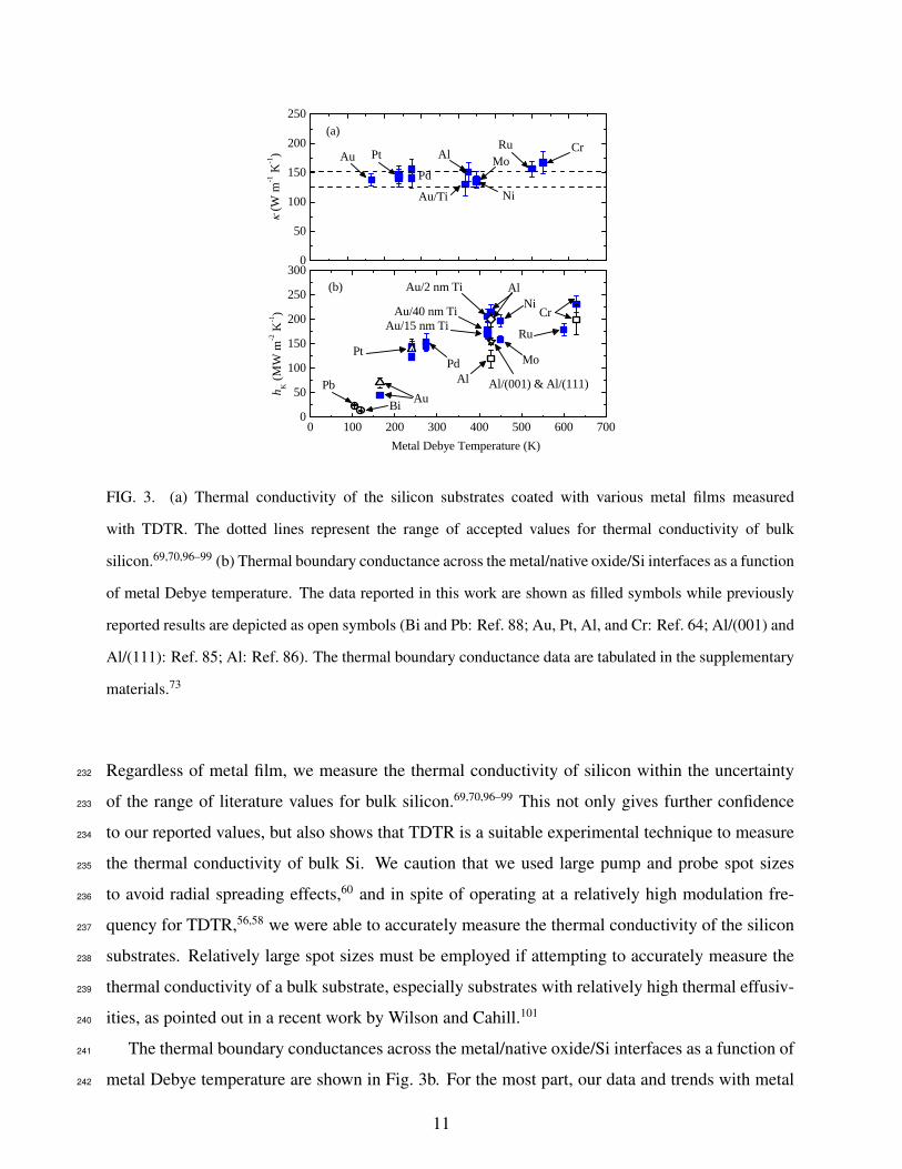
best fit silicon thermal conductivity as a function of the metal film Debye temperature100 in Fig. 3a.231
10
05 0
1 0 01 5 02 0 02 5 0
0 1 0 0 2 0 0 3 0 0 4 0 0 5 0 0 6 0 0 7 0 005 0
1 0 01 5 02 0 02 5 03 0 0
A u / T i N i
C r
� (W
m-1 K-1 ) A u R uP tP d
A l M o( a )
( b )
A l / ( 0 0 1 ) & A l / ( 1 1 1 )A lP t
A u / 1 5 n m T iA u / 4 0 n m T i N i C r
A u / 2 n m T i
M oP d
A l
A uP b
h K (M
W m-2 K-1 )
M e t a l D e b y e T e m p e r a t u r e ( K )
B i
R u
FIG. 3. (a) Thermal conductivity of the silicon substrates coated with various metal films measured
with TDTR. The dotted lines represent the range of accepted values for thermal conductivity of bulk
silicon.69,70,96–99 (b) Thermal boundary conductance across the metal/native oxide/Si interfaces as a function
of metal Debye temperature. The data reported in this work are shown as filled symbols while previously
reported results are depicted as open symbols (Bi and Pb: Ref. 88; Au, Pt, Al, and Cr: Ref. 64; Al/(001) and
Al/(111): Ref. 85; Al: Ref. 86). The thermal boundary conductance data are tabulated in the supplementary
materials.73
Regardless of metal film, we measure the thermal conductivity of silicon within the uncertainty232
of the range of literature values for bulk silicon.69,70,96–99 This not only gives further confidence233
to our reported values, but also shows that TDTR is a suitable experimental technique to measure234
the thermal conductivity of bulk Si. We caution that we used large pump and probe spot sizes235
to avoid radial spreading effects,60 and in spite of operating at a relatively high modulation fre-236
quency for TDTR,56,58 we were able to accurately measure the thermal conductivity of the silicon237
substrates. Relatively large spot sizes must be employed if attempting to accurately measure the238
thermal conductivity of a bulk substrate, especially substrates with relatively high thermal effusiv-239
ities, as pointed out in a recent work by Wilson and Cahill.101240
The thermal boundary conductances across the metal/native oxide/Si interfaces as a function of241
metal Debye temperature are shown in Fig. 3b. For the most part, our data and trends with metal242
11

Debye temperatures agree well with the previously reported values (open symbols).64,85–88 We will243
examine this in terms of phonon accumulation and transport physics in the next section, however,244
we note that these data provide first-reported values for hK across several transition metal/native245
oxide/Si interfaces, which are important for an array of applications due to the wide spread use of246
silicon and metallized silicon contacts.247
As another aside, it is interesting to note that the inclusion of Ti adhesion layers between Au248
and native oxide/Si increases the thermal boundary conductance substantially, as we have reported249
recently.66 We tested 3 different Au/Ti/native oxide/Si samples with different Ti thicknesses (2,250
15, and 40 nm). Within experimental uncertainty, we measure the same thermal boundary conduc-251
tance for each sample. The very similar agreement among the 2, 15 and 40 nm Ti cases suggests252
that the phonons in Ti play a role in hK at thicknesses as small as 2 nm.253
IV. ANALYSES OF EXPERIMENTAL DATA AND PHONON TRANSMISSION COEFFICIENT254
ACROSS METAL/NATIVE OXIDE/SILICON AND METAL/SAPPHIRE INTERFACES255
We can now analyze the data in Fig. 3b to quantify various aspects of thermal boundary con-256
ductance accumulation. The different metal films’ cutoff frequencies vary between 13.5 and 60257
Trad s−1. This provides a varying “bandwidth” of phonons that are incident on the metal/native258
oxide/silicon interface where each metal has a corresponding dispersion curve defined over the259
entire metal Brillouin zone and of maximum cutoff frequency less than or equal to 60 Trad s−1.260
However, the formulation in Section II derives the accumulation of Kapitza conductance assuming261
a single dispersion in the metal side. As a result, we can not directly compare the measurement re-262
sults on Kapitza conductance to the accumulation function defined earlier. Instead, we reformulate263
the accumulation function to account for the varying dispersion relation by making hK a function264
of the phonon group velocity in side 1. In the most general case Eq. 1 is rewritten:265
hK (ωmin,j, ωmax,j, υ1,j (ω, ωmin,j, ωmax,j)) =∑j
ωmax,j∫ωmin,j
∂q1,j (υ1,j (ω, ωmin,j, ωmax,j))
∂Tζ1→2 (υ1,j (ω, ωmin,j, ωmax,j)) dω
(8)
where the dependence of υ1,j on ωmin,j and ωmax,j is to emphasize that while υ1,j is dependent266
on ω, the variable of integration, its domain of definition, [ωmin,j , ωmax,j], is also variable. Using267
the same approach as in Section II we can also separate a weighted average of the transmission268
12

coefficient and simplify the above equation to:269
hK (υ1 (ωmax)) = QT (υ1 (ωmax)) ζ1→2 (υ1 (ωmax)) (9)
where270
QT (υ1 (ωmax)) =
ωmax∫0
∂q1 (υ1 (ωmax))
∂Tdω (10)
and we dropped the dependence on ω and the different cutoff frequencies and set the lower inte-271
gration limit to zero for simplicity. Defining a generic expression for υ1 and varying the cutoff272
frequency in the metal allows us to compare hK (υ1 (ωmax)) to the experimental measurements on273
different metals. In this case, hK (υ1 (ωmax)) is thought of as the un-normalized Kapitza conduc-274
tance accumulation across metal/Si interface.275
In Eq. 9, hK (υ1 (ωmax)) and QT (υ1 (ωmax)) are calculated assuming a sine-type dispersion276
for the metal phonons and using the polynomial fitted dispersion for silicon. Assuming a sine-type277
dispersion in the metal allows us to continuously vary the approximated phonon spectrum in the278
metal film by simply changing the cutoff frequency in the dispersion calculations,102 yielding a279
model input for the metal phonon flux in Eq. 9. The dispersion curves used in this calculation280
are shown in Fig. 2(b). For these calculations, we assume a ratio of longitudinal to transverse cut281
off frequencies in the metal based on the ratio of cutoff frequencies in Al and assume the lattice282
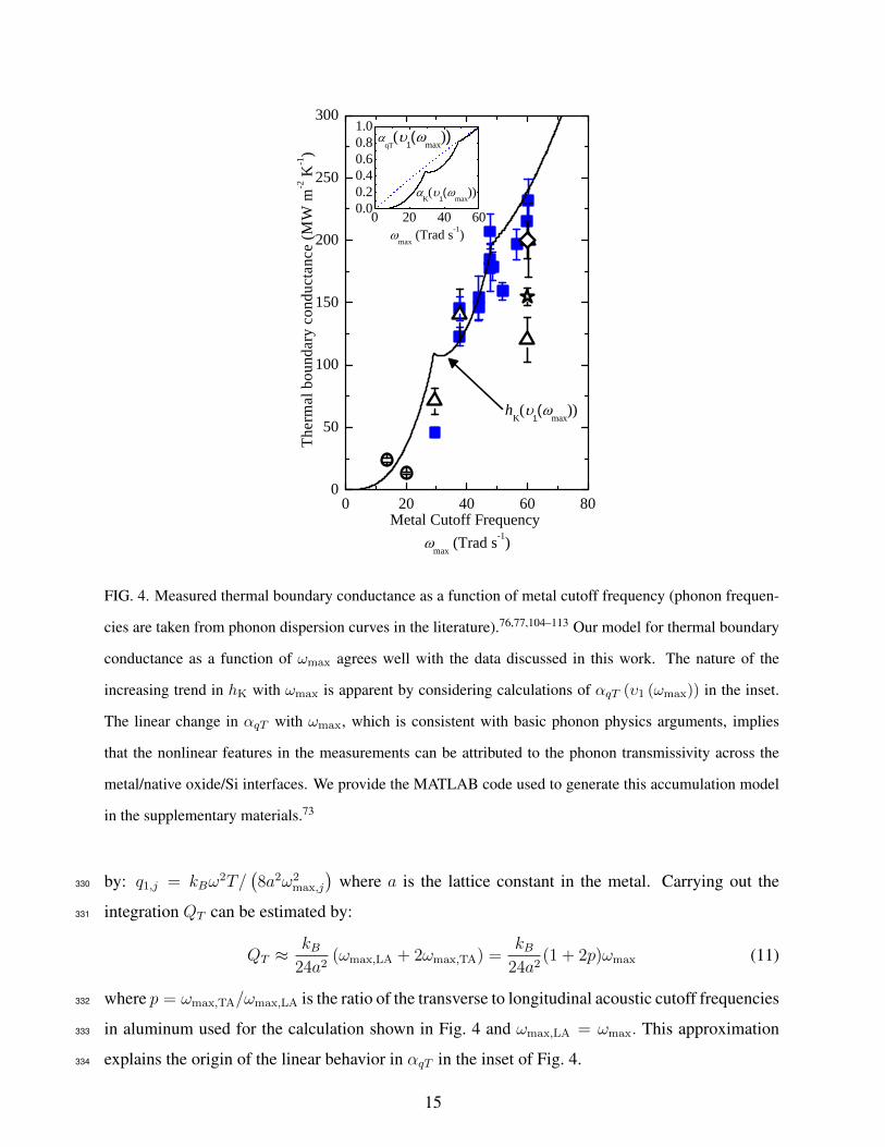
constant to be that of Al. The solid line in Fig. 4 shows the computed values of hK (υ1 (ωmax))283
along with the data from Fig. 3b. It is important to understand that the model plotted in Fig. 4 is284
not the mathematically known accumulation function and is thus different from the model plotted285
in Fig. 1. However, to a first approximation, the data and model in Fig. 4 “mimic” the accumu-286
lated phonon thermal boundary conductance across metal/Si interfaces. In this case, the different287
metal films change the accumulated frequency, so metal films with higher ωmax simply increase288
the frequencies of phonons in silicon that contribute to hK. The difference between the formula-289
tion in this section and that in Section II can be further understood from the difference between the290
dispersion curves and the ω − k space over which the integration is carried out shown in Fig. 2.291
While we used a single dispersion curve for the calculation of αK (ωα) in Section II, for each point292
of abscissa ωmax on the solid line plotted in Fig. 4, there corresponds a sine-type dispersion curve293
defined over [0, ωmax] and over the entire Brillouin zone in the metal side. In Fig. 2(b), the shaded294
area represents the k − ω space over which the integration is carried when ωmax = 40 Trad s−1295
and υ1 (ωmax) is given by the dispersion curve contained within the shaded region. Points A′ and296
13

B′ will coincide with A and B and the dispersion curves in the shaded region will coincide with297
that in the solid rectangle when ωmax = 70 Trad s−1. Our model prediction for the thermal bound-298
ary conductance accumulation shown in Fig. 4 agrees well with our experimental data, especially299
considering the simplicity of our approach and phonon dispersion assumptions that we used in this300
procedure. We note that no fitting parameters are used in this model.301
The isotropic solid assumption used in the calculation of the DMM is acceptable for cubic302
structures,77 however, bulk Ti and Ru have hcp crystal structure. Furthermore, thin Ti films can303
exhibit fcc, hcp, or a mix of hcp and fcc structures as has been shown in Al/Ti bilayers103 depend-304
ing on the film thickness. With the lack of literature on the crystal structure of thin Au/Ti bilayers,305
it is hard to assess the applicability of the isotropic solid assumption to the Au/Ti/Si samples char-306
acterized. However, the agreement between Kapitza conductance measurement on Au/Ti/Si and307
Ru/Si with the other metals with cubic structures over the range of cutoff frequencies may justify308
this assumption. We also note that while a Sine-type dispersion is valid for simple cubic structures,309
all the metals measured had fcc, bcc, or hcp structures. To check this approximation, we compare310
the Kapitza conductance across Al/Si and Au/Si interfaces using Sine and real type dispersions.311
The result shows that the ratio of Sine to real dispersion Kapitza conductances is 0.96 for Al/Si312
and 1.04 for Au/Si. Noting the excellent agreement between Sine and real dispersion and the fact313
that Al and Au have fcc structures, suggest that the use of a Sine dispersion is an acceptable ap-314
proximation.315
The inset of Fig. 4 shows normalized hK (υ1 (ωmax)), denoted by αK (υ1 (ωmax)), and the316317
normalized model calculations for QT (υ1 (ωmax)), denoted by αqT (υ1 (ωmax)), normalized to the318
values of hK (υ1 (ωmax)) and QT (υ1 (ωmax)) at the maximum cutoff frequency (60 Trad s−1), re-319
spectively. The accumulated temperature derivative of the phonon flux increases monotonically320
with phonon cutoff frequency, ωmax, as seen in the inset of Fig. 4. Even though this is a prediction321
from our model, this result is not surprising since to a first approximation, the cutoff frequency of322
metals with one atomic basis will directly scale with sound velocity and is related to the phonon323
density of states. At room temperature, the metals considered in this work can be considered324
in or near the classical limit (even for higher Debye temperature metals, such as Al and Cr, as325
their heat capacities are relatively flat around room temperature, justifying this assumption). In326
this case, the Bose-Einstein distribution can be estimated by: f = kBT/~ω. Using the isotropic327
solid expression for the density of states given by D1,j (ω) = ω2/(2π2υ31,j (ω)
)and invoking the328
Debye approximation for this analytical example, the phonon flux in the metal can be estimated329
14
0 2 0 4 0 6 0 8 00
5 0
1 0 0
1 5 0
2 0 0
2 5 0
3 0 0
0 2 0 4 0 6 00 . 00 . 20 . 40 . 60 . 81 . 0
�K ( �1(� m a x ) )
� q T ( �1(�m a x ) )
h K ( �1(�m a x ) )
Therm
al bou
ndary
cond
uctanc
e (MW
m-2 K-1 )
M e t a l C u t o f f F r e q u e n c y �m a x ( T r a d s - 1 )
� m a x ( T r a d s - 1 )
FIG. 4. Measured thermal boundary conductance as a function of metal cutoff frequency (phonon frequen-
cies are taken from phonon dispersion curves in the literature).76,77,104–113 Our model for thermal boundary
conductance as a function of ωmax agrees well with the data discussed in this work. The nature of the
increasing trend in hK with ωmax is apparent by considering calculations of αqT (υ1 (ωmax)) in the inset.
The linear change in αqT with ωmax, which is consistent with basic phonon physics arguments, implies
that the nonlinear features in the measurements can be attributed to the phonon transmissivity across the
metal/native oxide/Si interfaces. We provide the MATLAB code used to generate this accumulation model
in the supplementary materials.73
by: q1,j = kBω2T/
(8a2ω2
max,j
)where a is the lattice constant in the metal. Carrying out the330
integration QT can be estimated by:331
QT ≈kB
24a2(ωmax,LA + 2ωmax,TA) =
kB24a2
(1 + 2p)ωmax (11)
where p = ωmax,TA/ωmax,LA is the ratio of the transverse to longitudinal acoustic cutoff frequencies332
in aluminum used for the calculation shown in Fig. 4 and ωmax,LA = ωmax. This approximation333
explains the origin of the linear behavior in αqT in the inset of Fig. 4.334
15

0 1 0 2 0 3 0 4 0 5 0 6 0 7 0 8 005 0
1 0 01 5 02 0 02 5 03 0 03 5 04 0 04 5 05 0 0
C rS i l i c o n s u b s t r a t eS a p p h i r e s u b s t r a t e
A lA u / 2 n m T i
P dP tTh
ermal b
ound
ary co
nduct
ance (
MW m
-2 K-1 )
M e t a l C u t o f f F r e q u e n c y , �m a x ( T r a d s - 1 )
FIG. 5. Measured thermal boundary conductance across various metal/native oxide/Si and metal/sapphire
interfaces as a function of metal cutoff frequency. The measured data show that the magnitude of the
thermal boundary conductance across solid interfaces are not necessarily solely driven by the “phonon
spectral mismatch”, but also are related to the phonon energies and velocities incident on the interface.
This brings to light one of the first conclusions that we find from our accumulation analysis: the335
magnitudes of thermal boundary conductances across solid interfaces are not necessarily dictated336
by the “phonon mismatch” of the materials, but are directly correlated to the temperature derivative337
of the phonon flux impinging on the interface. Accordingly, thermal boundary conductance across338
interfaces comprised of materials that have a larger phonon mismatch (for example, based on339
Debye temperature ratio) will not necessarily be smaller than hK across interfaces that have a340
smaller mismatch. The actual value of hK will depend on the phonon flux (energies and velocities).341
This conclusion is further strengthened by considering the measured value of thermal boundary342
conductance across metal/sapphire interfaces compared to metal/native oxide/silicon interfaces,343
shown in Fig. 5. As an aside, the experimental procedures for fabricating and testing these various344
metal/sapphire interfaces were identical to that discussed in Section III, and each pair of substrates345
shown in Fig. 5 were coated in the same deposition chamber. It is evident that these metal/sapphire346
thermal boundary conductance data can be larger than the metal/Si data, even though the “phonon347
mismatch” is greater by a Debye temperature argument (note, for example, the Al and Cr data).348
This result reinforces the findings from our previous molecular dynamics work.62349
Referring back to our discussion regarding αqT in the inset in Fig. 4, the linear increase in the350351
accumulation of this quantity will not change for different substrates. Therefore, the difference352
16
between the metal/Si and metal/sapphire data can be attributed to the substrate modes and the353
average phonon transmission across the interface in the frequency range of the metal phonon354
spectra, ζ1→2 (υ1 (ωmax)). We can rearrange Eq. 9 to find that ζ1→2 (υ1 (ωmax)) is simply a function355
of hK and QT , represented as356
ζ1→2 (υ1 (ωmax)) =hKQT
. (12)
As demonstrated, the thermal boundary conductance measurements on the various samples con-357
struct the thermal boundary conductance accumulation function (i.e., the measured data are the358
quantity hK). Since if we can accurately predict ∂q1/∂T (and hence QT ), we can determine the359
average of phonon transmission in the phonon spectrum of the metal by using the measured TDTR360
data in Eq. 12. Values for ζ1→2 for the metal/native oxide/silicon and metal/sapphire are shown361
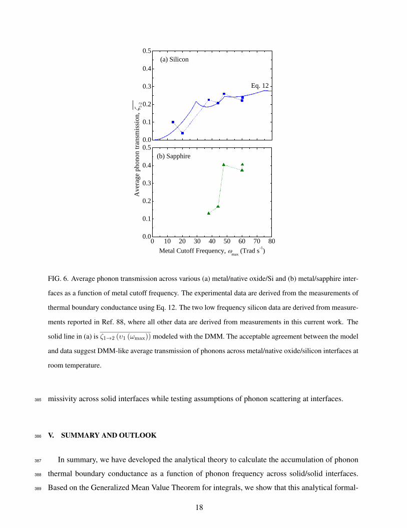
in Fig. 6. Note that these values did not require any information about phonon distributions in362363
the substrate. Nevertheless, the quantity shown in Fig. 6a and b, gives direct insight into how364
phonons couple energy across solid interfaces comprised of silicon with a native oxide layer and365
sapphire, respectively. For example, our data indicate that the phonon transmission coefficients366
across metal/native oxide/Si and metal/sapphire interfaces are relatively constant for phonon fre-367
quencies greater than∼ 30 Trad s−1 and∼ 45 Trad s−1, respectively. This implies that the increase368
in thermal boundary conductance that is observed when the maximum phonon frequency in the369
metal goes beyond these two frequencies is due to an increase in phonon flux from high frequency370
modes and velocities in the metal, and not due to an increase in phonon transmission or better371
“matching” of the phonon modes near the interface. Thus the change in the metal phonon flux is372
what dominates interface conductance for high frequency phonons. The fact that ζ1→2 (υ1 (ωmax))373
flattens at 2 different frequencies for Si and sapphire is directly attributed to the substrate modes374
and phonon coupling between the metal film and the substrate.375
Figure 6a also shows the calculations of ζ1→2 (υ1 (ωmax)) for metal/silicon interfaces using the376
assumptions of the DMM. We show acceptable agreement between the DMM calculations and our377
experimentally derived data of ζ1→2 (υ1 (ωmax)), which provides an additional platform for us to378
validate the DMM assumptions of phonon transmissivity beyond simply comparing DMM calcu-379
lations of hK to measured data. The model and data agreement in Fig. 6(a) support our assertions380
in the DMM calculations, namely that phonons scatter diffusively and elastically at metal/native381
oxide/silicon interfaces. We do not attempt to model ζ1→2 (υ1 (ωmax)) for the sapphire data using382
the DMM due to the non-cubic crystal structure and additional assumptions that we must apply.85383
Looking ahead, this approach provides a convenient method to determine average phonon trans-384
17
0 . 0
0 . 1
0 . 2
0 . 3
0 . 4
0 . 5
0 1 0 2 0 3 0 4 0 5 0 6 0 7 0 8 00 . 0
0 . 1
0 . 2
0 . 3
0 . 4
0 . 5
E q . 1 2
( a ) S i l i c o n
( b ) S a p p h i r e
Avera
ge pho
non tra
nsmiss
ion, � 1-2
M e t a l C u t o f f F r e q u e n c y , �m a x ( T r a d s - 1 )
FIG. 6. Average phonon transmission across various (a) metal/native oxide/Si and (b) metal/sapphire inter-
faces as a function of metal cutoff frequency. The experimental data are derived from the measurements of
thermal boundary conductance using Eq. 12. The two low frequency silicon data are derived from measure-
ments reported in Ref. 88, where all other data are derived from measurements in this current work. The
solid line in (a) is ζ1→2 (υ1 (ωmax)) modeled with the DMM. The acceptable agreement between the model
and data suggest DMM-like average transmission of phonons across metal/native oxide/silicon interfaces at
room temperature.
missivity across solid interfaces while testing assumptions of phonon scattering at interfaces.385
V. SUMMARY AND OUTLOOK386
In summary, we have developed the analytical theory to calculate the accumulation of phonon387
thermal boundary conductance as a function of phonon frequency across solid/solid interfaces.388
Based on the Generalized Mean Value Theorem for integrals, we show that this analytical formal-389
18
ism can be related to the average interfacial phonon transmission across interfaces by considering390
the accumulation of the the temperature derivative of the phonon flux incident on the interface. We391
test our theory with a series of thermal boundary conductance measurements across metal/native392
oxide/silicon and metal/sapphire interfaces. We use the measured values of thermal boundary393
conductance and calculations of the temperature derivative of the phonon flux to back out the394
average interfacial phonon transmission across the interfaces. Across the metal/native oxide/Si395
interfaces, we show good agreement with calculations of average spectral phonon transmission396
predicted from the DMM. This approach represents a relatively straight forward method to analyze397
thermal boundary conductance data across a series of carefully prepared interfaces and to quantify398
the spectral phonon transmission component to thermal boundary conductance, a quantity that has399
not been previously measured above superconducting temperatures.400
In addition to the advancement in experimental analysis of thermal boundary conductance data401
and the development of a formalism for frequency accumulation of phonon thermal boundary402
conductance across interfaces, we also report several experimentally supported conclusions that403
advance the field of phonon interactions at interfaces. As a broad conclusion, we show that the404
magnitudes of thermal boundary conductances across solid interfaces are not necessarily dictated405
by the “phonon mismatch” of the materials, but are directly correlated to temperature derivative406
of the phonon flux impinging on the interface. This interplay between transmission due to phonon407
mismatch and phonon flux on the magnitude of phonon thermal boundary conductance changes408
spectrally, and for metal/native oxide/silicon and metal/sapphire interfaces, the phonon trans-409
missivity is flat for high frequency phonons in the substrate, indicating that the changing metal410
phonon flux dominates the phonon thermal boundary conductance for high frequency phonons.411
In performing this analysis, we also validate the assumptions of the DMM for metal/native ox-412
ide/silicon interfaces based on comparison of the spectrally averaged phonon transmission. In413
our experimental measurements, we also provide measurements of thermal boundary conductance414
across metal/native oxide/silicon and metal/sapphire interfaces that have not previously been re-415
ported. In doing so, we show that for the Au/Ti/Si interface, the influence of phonons in the Ti416
adhesion layer can affect the thermal boundary conductance for layers as thin as 2 nm. Finally,417
we demonstrate the utility of TDTR for measuring the thermal conductivity of bulk Si substrates,418
which gives further demonstrates the capability of TDTR to measure the thermal conductivity of419
bulk, homogeneous materials with high thermal effusivity.420
The utility of this approach lies in the generality in which it was developed. A similar approach421
19
can be used with TDTR measurements of thermal boundary conductance across any interface in422
which this quantity is measurable (i.e., relatively high conductivity substrates). This could be very423
useful for understanding phonon transmission and interactions across interfaces comprised of a424
wide array of single crystals, dilute alloys, and some superlattices. When the thermal conductivity425
of the materials comprising the interface becomes too low, it is difficult to resolve the thermal426
boundary conductance, so advances in basic metrology must be achieved to extend this approach427
to low thermal conductivity materials, such as some complex oxides, soft materials (e.g., poly-428
mers), amorphous materials, and liquids.429
Finally, this study sets the stage for robust theoretical and computational advances in phonon430
scattering and transmission across interfaces. A more computationally rigorous calculation of431
phonon flux accounting for the deviation from equilibrium can enhance the accuracy of our432
model.114,115 Including contributions due to inelastic scattering processes and using a more real-433
istic dispersion could also account for additional deviations between our model and experimental434
measurements, especially when using this approach with more complicated interfaces not com-435
prised of a simple metal in which the phonon flux can be relatively well predicted.19,20,24,116 In436
addition, it should be possible to study the accumulation of thermal boundary conductance and437
the average interfacial transmission with molecular dynamics, which could then be used to re-438
late these trends to pure spectral transmission (i.e., not bandwidth averaged). This could provide439
a systematic computational approach to understand more complex phonon scattering processes440
such as inelastic scattering20,21,88,116 or transmission across disordered interfaces,4 which, when441
coupled with this experimental approach, will provide great advances in the understanding of442
phonon transport and thermal conductance in nanosystems.443
444
ACKNOWLEDGMENTS445
Authors would like to thank Mia Blea-Kirby from Sandia National Laboratories for her as-446
sistance in film deposition. This work was supported by the Office of Naval Research Young447
Investigator Program (N00014-13-4-0528), the National Science Foundation (CBET-1339436),448
Commonwealth Research Commercialization Fund (CRCF) of Virginia, and the 4-VA mini-grant449
for university collaboration in the Commonwealth of Virginia. This project was supported by Fi-450
nancial Assistance Award No. 01-79-14214, awarded by U.S. Department of Commerce Economic451
20
Development Administration, to the University of Virginia. The content is solely the responsibility452
of the authors and does not necessarily represent the official views of the U.S. Department of Com-453
merce Economic Development Administration. Sandia National Laboratories is a multiprogram454
laboratory managed and operated by Sandia Corporation, a wholly owned subsidiary of Lockheed455
Martin Corporation, for the U.S. Department of Energy National Nuclear Security Administration456
under Contract No. DE-AC04-94AL85000.457
∗ These authors contributed equally to this work458
1 D. G. Cahill, W. K. Ford, K. E. Goodson, G. D. Mahan, A. Majumdar, H. J. Maris, R. Merlin, and S. R.460
Phillpot, Journal of Applied Physics 93, 793 (2003).461
2 D. G. Cahill, P. V. Braun, G. Chen, D. R. Clarke, S. Fan, K. E. Goodson, P. Keblinski, W. P. King,462
G. D. Mahan, A. Majumdar, H. J. Maris, S. R. Phillpot, E. Pop, and L. Shi, Applied Physics Reviews463
1, 011305 (2014).464
3 P. M. Norris, N. Q. Le, and C. H. Baker, Journal of Heat Transfer 135, 061604 (2013).465
4 P. E. Hopkins, International Scholarly Research Notices 2013 (2013), /10.1155/2013/682586.466
5 B. Krenzer, A. Hanisch-Blicharski, P. Schneider, T. Payer, S. Mollenbeck, O. Osmani, M. Kammler,467
R. Meyer, and M. Horn-vonHoegen, Physical Review B 80, 024307 (2009).468
6 A. Hanisch, B. Krenzer, T. Pelka, S. Mollenbeck, and M. Horn-vonHoegen, Physical Review B 77,469
125410 (2008).470
7 R. M. Costescu, M. A. Wall, and D. G. Cahill, Physical Review B 67, 054302 (2003).471
8 P. L. Kapitza, Zhurnal eksperimentalnoi i teoreticheskoi fiziki 11, 1 (1941).472
9 E. T. Swartz and R. O. Pohl, Reviews of Modern Physics 61, 605 (1989).473
10 I. M. Khalatnikov, Journal of Experimental and Theoretical Physics (1952).474
11 J. D. N. Cheeke, H. Ettinger, and B. Hebral, Canadian Journal of Physics 54, 1749 (1976).475
12 R. S. Prasher and P. E. Phelan, Journal of heat transfer 123, 105 (2001).476
13 N. Q. Le, J. C. Duda, T. S. English, P. E. Hopkins, T. E. Beechem, and P. M. Norris, Journal of Applied477
Physics 111, 084310 (2012).478
14 J. C. Duda, J. L. Smoyer, P. M. Norris, and P. E. Hopkins, Applied Physics Letters 95, 031912 (2009).479
15 T. Beechem, S. Graham, P. Hopkins, and P. Norris, Applied Physics Letters 90, 054104 (2007).480
21
16 T. Beechem, J. C. Duda, P. E. Hopkins, and P. M. Norris, Applied Physics Letters 97, 061907 (2010).481
17 R. S. Prasher and P. E. Phelan, Journal of Heat Transfer 123, 105 (2001).482
18 P. E. Hopkins and P. M. Norris, Nanoscale and Microscale Thermophysical Engineering 11, 247 (2007).483
19 P. Reddy, K. Castelino, and A. Majumdar, Applied Physics Letters 87, 211908 (2005).484
20 P. E. Hopkins, Journal of Applied Physics 106, 013528 (2009).485
21 P. E. Hopkins, J. C. Duda, and P. M. Norris, Journal of Heat Transfer 133, 062401 (2011).486
22 J. C. Duda, P. M. Norris, and P. E. Hopkins, Journal of Heat Transfer 133, 074501 (2011).487
23 C. Dames and G. Chen, Journal of Applied Physics 95, 682 (2004).488
24 P. E. Hopkins and P. M. Norris, Journal of Heat Transfer 131, 022402 (2009).489
25 T. Beechem and P. E. Hopkins, Journal of Applied Physics 106, 124301 (2009).490
26 P. E. Phelan, Journal of Heat Transfer 120, 37 (1998).491
27 R. S. Prasher, Applied Physics Letters 94, 041905 (2009).492
28 G. C. Loh, B. K. Tay, and E. H. T. Teo, Applied Physics Letters 97, 121917 (2010).493
29 G. Chen, Nanoscale Energy Transport and Conversion: A Parallel Treatment of Electrons, Molecules, Phonons, and Photons494
(Oxford University Press, New York, 2005).495
30 X. Wu and T. Luo, Journal of Applied Physics 115, 014901 (2014).496
31 R. J. Stevens, L. V. Zhigilei, and P. M. Norris, International Journal of Heat and Mass Transfer 50,497
3977 (2007).498
32 J. C. Duda, T. S. English, E. S. Piekos, W. A. Soffa, L. V. Zhigilei, and P. E. Hopkins, Physical Review499
B 84, 193301 (2011).500
33 T. S. English, J. C. Duda, J. L. Smoyer, D. A. Jordan, P. M. Norris, and L. V. Zhigilei, Physical Review501
B 85, 035438 (2012).502
34 R. N. Salaway, P. E. Hopkins, P. M. Norris, and R. J. Stevens, International Journal of Thermophysics503
29, 1987 (2008).504
35 X. W. Zhou, R. E. Jones, J. C. Duda, and P. E. Hopkins, Physical Chemistry Chemical Physics 15,505
11078 (2013).506
36 X. W. Zhou, R. E. Jones, C. J. Kimmer, J. C. Duda, and P. E. Hopkins, Physical Review B 87, 094303507
(2013).508
37 R. E. Jones, J. C. Duda, X. W. Zhou, C. J. Kimmer, and P. E. Hopkins, Applied Physics Letters 102,509
183119 (2013).510
38 E. S. Landry and A. J. H. McGaughey, Physical Review B 80, 165304 (2009).511
22
39 Z. Y. Ong and E. Pop, Journal of Applied Physics 108, 103502 (2010).512
40 Z.-Y. Ong and E. Pop, Physical Review B 81, 155408 (2010).513
41 M. Shen, W. J. Evans, D. Cahill, and P. Keblinski, Physical Review B 84, 195432 (2011).514
42 L. Hu, L. Zhang, M. Hu, J. S. Wang, B. Li, and P. Keblinski, Physical Review B 81, 235427 (2010).515
43 M. Hu, P. Keblinski, and P. K. Schelling, Physical Review B 79, 104305 (2009).516
44 P. K. Schelling, S. R. Phillpot, and P. Keblinski, Applied Physics Letters 80, 2484 (2002).517
45 W. E. Pickett, J. L. Feldman, and J. Deppe, Modeling and Simulation in Materials Science and Engi-518
neering 4, 409 (1996).519
46 B. C. Daly, H. J. Maris, K. Imamura, and S. Tamura, Physical Review B 66, 024301 (2002).520
47 S. H. Choi and S. Maruyama, International Journal of Thermal Sciences 44, 547 (2005).521
48 C.-J. Twu and J.-R. Ho, Physical Review B 67, 205422 (2003).522
49 A. Maiti, G. Mahan, and S. Pantelides, Solid State Communications 102, 517 (1997).523
50 F. Yang and C. Dames, Physical Review B 87, 035437 (2013).524
51 A. J. Minnich, Physical Review Letters 109, 205901 (2012).525
52 A. S. Henry and G. Chen, Computational and Theoretical Nanoscience 5, 1 (2008).526
53 K. Esfarjani, G. Chen, and H. T. Stokes, Physical Review B 84, 085204 (2011).527
54 Z. Tian, J. Garg, K. Esfarjani, T. Shiga, J. Shiomi, and G. Chen, Phys. Rev. B 85, 184303 (2012).528
55 M. Zebarjadi, K. Esfarjani, M. S. Dresselhaus, Z. F. Ren, and G. Chen, Energy and Environmental529
Science 5, 5147 (2012).530
56 K. T. Regner, D. P. Sellan, Z. Su, C. H. Amon, A. J. H. McGaughey, and J. A. Malen, Nature Commu-531
nications 4, 1640 (2013).532
57 K. T. Regner, S. Majumdar, and J. A. Malen, Review of Scientific Instruments 84, 064901 (2013).533
58 Y. K. Koh and D. G. Cahill, Physical Review B 76, 075207 (2007).534
59 X. Liu, J. L. Feldman, D. G. Cahill, R. S. Crandall, N. Bernstein, D. M. Photiadis, M. J. Mehl, and535
D. A. Papaconstantopoulos, Physical Review Letters 102, 035901 (2009).536
60 A. J. Minnich, J. A. Johnson, A. J. Schmidt, K. Esfarjani, M. S. Dresselhaus, K. A. Nelson, and537
G. Chen, Physical Review Letters 107, 095901 (2011).538
61 M. E. Siemens, Q. Li, R. Yang, K. A. Nelson, E. H. Anderson, M. M. Murnane, and H. C. Kapteyn,539
Nature Materials 9, 26 (2010).540
62 J. C. Duda, C. J. Kimmer, W. A. Soffa, X. W. Zhou, R. E. Jones, and P. E. Hopkins, Journal of Applied541
Physics 112, 093515 (2012).542
23
63 P. M. Norris and P. E. Hopkins, Journal of Heat Transfer 131, 043207 (2009).543
64 R. J. Stevens, A. N. Smith, and P. M. Norris, Journal of Heat Transfer 127, 315 (2005).544
65 R. J. Stoner and H. J. Maris, Physical Review B 48, 16373 (1993).545
66 J. C. Duda, C.-Y. P. Yang, B. M. Foley, R. Cheaito, D. L. Medlin, R. E. Jones, and P. E. Hopkins,546
Applied Physics Letters 102, 081902 (2013).547
67 M. D. Losego, M. E. Grady, N. R. Sottos, D. G. Cahill, and P. V. Braun, Nature Materials 11, 502548
(2012).549
68 P. E. Hopkins, M. Baraket, E. V. Barnat, T. E. Beechem, S. P. Kearney, J. C. Duda, J. T. Robinson, and550
S. G. Walton, Nano Letters 12, 590 (2012).551
69 C. Y. Ho, R. W. Powell, and P. E. Liley, Journal of Physical and Chemical Reference Data 1, 279552
(1972).553
70 F. Incropera and D. P. DeWitt, Fundamentals of Heat and Mass Transfer, 4th ed. (Wiley and Sons, Inc.,554
New York, 1996).555
71 D. E. Gray, American Institute of Physics Handbook, 3rd ed. (McGraw Hill, New York, 1972).556
72 K. D. Joshi, Calculus for Scientists and Engineers: An Analytical Approach (Narosa, 2002) pp. 448–557
449.558
73 See Supplementary Materials at [URL will be inserted by publisher] for more information.559
74 J. C. Duda, P. E. Hopkins, J. L. Smoyer, M. L. Bauer, T. S. English, C. B. Saltonstall, and P. M. Norris,560
Nanoscale and Microscale Thermophysical Engineering 14, 21 (2010).561
75 J. C. Duda, T. Beechem, J. L. Smoyer, P. M. Norris, and P. E. Hopkins, Journal of Applied Physics562
108, 073515 (2010).563
76 J. W. Lynn, H. G. Smith, and R. M. Nicklow, Physical Review B 8, 3493 (1973).564
77 G. Gilat and R. M. Nicklow, Physical Review 143, 487 (1966).565
78 W. Weber, Physical Review B 15, 4789 (1977).566
79 D. P. Sellan, J. E. Turney, A. J. H. McGaughey, and C. H. Amon, Journal of Applied Physics 108,567
113524 (2010).568
80 E. Dechaumphai, D. Lu, J. J. Kan, J. Moon, E. Fullerton, Z. Liu, and R. Chen, Nano letters (2014),569
10.1021/nl500127c.570
81 L. Van Hove, Phys. Rev. 89, 1189 (1953).571
82 J. B. Hertzberg, M. Aksit, O. O. Otelaja, D. A. Stewart, and R. D. Robinson, Nano Letters 14, 403572
(2014), http://pubs.acs.org/doi/pdf/10.1021/nl402701a.573
24

83 G. Chen, Applied Physics Letters 82, 991 (2003).574
84 S. Simons, Journal of Physics C: Solid State Physics 7, 4048 (1974).575
85 P. E. Hopkins, T. E. Beechem, J. C. Duda, K. Hattar, J. F. Ihlefeld, M. A. Rodriguez, and E. S. Piekos,576
Physical Review B 84, 125408 (2011).577
86 P. E. Hopkins, K. Hattar, T. Beechem, J. F. Ihlefeld, D. L. Medlin, and E. S. Piekos, Applied Physics578
Letters 98, 231901 (2011).579
87 J. C. Duda and P. E. Hopkins, Applied Physics Letters 100, 111602 (2012).580
88 H.-K. Lyeo and D. G. Cahill, Phys. Rev. B 73, 144301 (2006).581
89 P. E. Hopkins, J. C. Duda, C. W. Petz, and J. A. Floro, Physical Review B 84, 035438 (2011).582
90 P. E. Hopkins, L. M. Phinney, J. R. Serrano, and T. E. Beechem, Physical Review B 82, 085307 (2010).583
91 C. S. Gorham, K. Hattar, R. Cheaito, T. Beechem, J. C. Duda, J. F. Ihlefeld, D. L. Medlin, E. S. Piekos,584
and P. E. Hopkins, under review (2014).585
92 A. J. Schmidt, X. Chen, and G. Chen, Review of Scientific Instruments 79, 114902 (2008).586
93 D. G. Cahill, Review of Scientific Instruments 75, 5119 (2004).587
94 P. E. Hopkins, J. R. Serrano, L. M. Phinney, S. P. Kearney, T. W. Grasser, and C. T. Harris, Journal of588
Heat Transfer 132, 081302 (2010).589
95 C. Thomsen, J. Strait, Z. Vardeny, H. J. Maris, J. Tauc, and J. J. Hauser, Physical Review Letters 53,590
989 (1984).591
96 R. G. Morris and J. G. Hust, Phys. Rev. 124, 1426 (1961).592
97 C. J. Glassbrenner and G. A. Slack, Phys. Rev. 134, A1058 (1964).593
98 D. R. Lide, CRC Handbook for Chemistry and Physics, 89th ed. (Internet Version, CRC Press/Taylor594
and Francis, Boca Raton, FL, 2008).595
99 J. H. Lienhard IV and J. H. Lienhard V, A Heat Transfer Textbook, 4th edition (Courier Dover Publica-596
tions, 2012).597
100 C. Kittel, Introduction to Solid State Physics, 7th ed. (John Wiley and Sons, Inc., New York, 1996).598
101 R. Wilson and D. G. Cahill, Nature communications 5 (2014), 10.1038/ncomms6075.599
102 G. Chen, Journal of Heat Transfer 119, 220 (1997).600
103 R. Banerjee, R. Ahuja, and H. L. Fraser, Phys. Rev. Lett. 76, 3778 (1996).601
104 B. N. Brockhouse, T. Arase, G. Caglioti, K. R. Rao, and A. D. B. Woods, Physical Review 128, 1099602
(1962).603
25
105 J. Braun, K. L. Kostov, G. Witte, L. Surnev, J. G. Skofronick, S. A. Safron, and C. Woll, Surface604
Science 372, 132 (1997).605
106 R. J. Birgeneau, J. Cordes, G. Dolling, and A. D. B. Woods, Physical Review 136, A1359 (1964).606
107 D. H. Dutton, B. N. Brockhouse, and A. P. Miller, Canadian Journal of Physics 50, 2915 (1972).607
108 A. P. Miller and B. N. Brockhouse, Canadian Journal of Physics 49, 704 (1971).608
109 W. M. Shaw and L. D. Muhlestein, Physical Review B 4, 969 (1971).609
110 R. Colella and B. W. Batterman, Physical Review B 1, 3913 (1970).610
111 E. D. Murray, S. Fahy, D. Prendergast, T. Ogitsu, D. M. Fritz, and D. A. Reis, Physical Review B 75,611
184301 (2007).612
112 Z.-Y. Zeng, C.-E. Hu, L.-C. Cai, X.-R. Chen, and F.-Q. Jing, Journal of Physical Chemistry B 114, 298613
(2010).614
113 C. Stassis, D. Arch, B. N. Harmon, and N. Wakabayashi, Physical Review B 19, 181 (1979).615
114 S. Merabia and K. Termentzidis, Phys. Rev. B 86, 094303 (2012).616
115 J. E. Turney, E. S. Landry, A. J. H. McGaughey, and C. H. Amon, Phys. Rev. B 79, 064301 (2009).617
116 P. E. Hopkins, R. J. Stevens, and P. M. Norris, Journal of Heat Transfer 130, 022401 (2008).618
26